EP1751329B1 - Verfahren zum ziehen von sic-einkristallen und sic-einkristall - Google Patents
Verfahren zum ziehen von sic-einkristallen und sic-einkristall Download PDFInfo
- Publication number
- EP1751329B1 EP1751329B1 EP05741354A EP05741354A EP1751329B1 EP 1751329 B1 EP1751329 B1 EP 1751329B1 EP 05741354 A EP05741354 A EP 05741354A EP 05741354 A EP05741354 A EP 05741354A EP 1751329 B1 EP1751329 B1 EP 1751329B1
- Authority
- EP
- European Patent Office
- Prior art keywords
- single crystal
- sic single
- growth
- plane
- substrate
- Prior art date
- Legal status (The legal status is an assumption and is not a legal conclusion. Google has not performed a legal analysis and makes no representation as to the accuracy of the status listed.)
- Expired - Fee Related
Links
Images

Classifications
-
- C—CHEMISTRY; METALLURGY
- C23—COATING METALLIC MATERIAL; COATING MATERIAL WITH METALLIC MATERIAL; CHEMICAL SURFACE TREATMENT; DIFFUSION TREATMENT OF METALLIC MATERIAL; COATING BY VACUUM EVAPORATION, BY SPUTTERING, BY ION IMPLANTATION OR BY CHEMICAL VAPOUR DEPOSITION, IN GENERAL; INHIBITING CORROSION OF METALLIC MATERIAL OR INCRUSTATION IN GENERAL
- C23C—COATING METALLIC MATERIAL; COATING MATERIAL WITH METALLIC MATERIAL; SURFACE TREATMENT OF METALLIC MATERIAL BY DIFFUSION INTO THE SURFACE, BY CHEMICAL CONVERSION OR SUBSTITUTION; COATING BY VACUUM EVAPORATION, BY SPUTTERING, BY ION IMPLANTATION OR BY CHEMICAL VAPOUR DEPOSITION, IN GENERAL
- C23C16/00—Chemical coating by decomposition of gaseous compounds, without leaving reaction products of surface material in the coating, i.e. chemical vapour deposition [CVD] processes
- C23C16/22—Chemical coating by decomposition of gaseous compounds, without leaving reaction products of surface material in the coating, i.e. chemical vapour deposition [CVD] processes characterised by the deposition of inorganic material, other than metallic material
- C23C16/30—Deposition of compounds, mixtures or solid solutions, e.g. borides, carbides, nitrides
- C23C16/32—Carbides
- C23C16/325—Silicon carbide
Definitions
- the present invention relates to a method of epitaxial growth of an SiC single crystal, in particular a 4H-SiC single crystal, on an SiC single crystal substrate, in particular a 4H-SiC single crystal substrate.
- SiC has a larger energy band gap compared with Si, so various technologies for production of high grade SiC single crystal suitable as a semiconductor material etc. has been proposed in Japanese Unexamined Patent Publication (Kokai) No. 2003-300797 , Japanese Unexamined Patent Publication (Kokai) No. 2003-300796 , Japanese Unexamined Patent Publication (Kokai) No. 2003-342099 , Japanese Unexamined Patent Publication (Kokai) No. 2001-181095 , Japanese Unexamined Patent Publication (Kokai) No. 10-17399 , etc.
- prevention of the surface defects of the above (1) is a major premise for practical use as a semiconductor material.
- SiC (0001) plane bottom plane of hexagonal crystal
- SiC crystals (polygonal) with different crystal structures will easily become mixed in the growth plane and high quality crystal cannot be obtained.
- step flow growth has been performed making the growth plane an angle inclined by several degrees from the (0001) plane (off-angle).
- the device properties such as triangular defects or carrot defects (device killers) and achieve stable epitaxial growth.
- step flow growth the crystal growth proceeds in steps in the lateral direction.
- the terrace area is large, so starting points of defects easily arise on the terrace surfaces and the defects grown from those starting points are taken into the epitaxial growth layer.
- pinholes due to large spiral dislocations called "micropipes" extending in the ⁇ 0001> axial direction are also passed on to the growth layer.
- Japanese Unexamined Patent Publication (Kokai) No. 2003-300797 discloses to make a plane inclined from the (11-20) plane by an off-angle of at least 3 degrees to not more than 60 degrees in any direction in the range of -45 degrees to 45 degrees in the ⁇ 1-100> axial direction centered about the ⁇ 0001> axis the epitaxial thin film growth plane. This improves the growth rate of the SiC single crystal, but has the problem that the influx of impurities cannot be reduced.
- An object of the present invention is to provide a method of epitaxial growth of a 4H-SiC single crystal enabling growth of an SiC single crystal with low defects and low impurities able to be used for a semiconductor material at a practical growth rate and a 4H-SiC single crystal obtained by the same.
- a method of growth of an SiC single crystal comprising growing a 4H-SiC single crystal on a 4H-SiC single crystal substrate by epitaxial growth while inclining an epitaxial growth plane of the substrate from a (0001) plane of the 4H-SiC single crystal by an off-angle of at least 12 degrees and less than 18 degrees in a ⁇ 11-20> axial direction.
- the off-angle is at least 12 degrees and not more than 25 degrees.
- the off-angle is at least 12 degrees and not more than 18 degrees.
- an SiC single crystal grown by a method of the present invention According to a second aspect of the invention, there is provided an SiC single crystal grown by a method of the present invention.
- a method of growth of an SiC single crystal comprising growing a 4H-SiC single crystal on a 4H-SiC single crystal substrate by epitaxial growth while inclining an epitaxial growth plane of the substrate from a (0001) plane of the 4H-SiC single crystal by an off-angle of at least 12 degrees and less than 30 degrees in a ⁇ 11-20> axial direction.
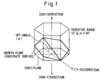
- FIG. 1 shows the epitaxial growth plane defined in the present invention.
- the figure shows the hexagonal crystal structure of a SiC single crystal.
- the substrate plane that is, the growth plane, is inclined from the bottom plane of the hexagonal crystal, that is, the (0001) plane, by exactly an off-angle in the ⁇ 11-20> axial direction.
- the off-angle is preferably at least 12 degrees and not more than 25 degrees, most preferably at least 12 degrees and not more than 18 degrees.
- an SiC single crystal grown by the above method is also provided.
- the inventors completed the present invention based on the novel discovery that by using a substrate having a plane inclined from the (0001) plane of a 4H-SiC single crystal by an off-angle of at least 12 degrees and less than 30 degrees in the ⁇ 11-20> axial direction as the epitaxial growth plane, it is possible to grow a low defect, low impurity 4H-SiC single crystal at a practical growth rate.
- the growth rate is improved and simultaneously an extremely flat growth layer can be obtained without roughening of the epitaxial growth surface.
- a growth plane with an off-angle of 12 degrees or more is not a step and ⁇ 0001 ⁇ terrace, but a specific plane determined by that off-angle. In this case, there is no mixture with different polytypes even if two-dimensional nucleus formation occurred at the growth surface. Further, since this is two-dimensional growth, no triangular-defects occur either.
- the triangular-defects which easily occurred at a growth plane with an off-angle of 4 to 8 degrees are substantially eliminated according to the present invention by making the off-angle at least 12 to less than 30 degrees. This is because if the off-angle is made larger, the terrace width of the crystal growth plane becomes smaller and the starting points for occurrence of defects on the terrace are greatly reduced. Further, since the density of the free bonding arms at the crystal surface differs from that at the (0001) plane, the efficiency of influx of impurities also changes. Specifically, the influx of N atoms is suppressed and fabrication of high purity crystal becomes easy.
- an extremely high quality epitaxial growth layer with low residual impurities (donors and acceptors) compared with conventional substrates with an off-angle of about 8 degrees can be obtained.
- the off-angle is about 15 degrees, the highest purity crystal is obtained.
- the micropipes present in the substrate are dissociated. This is observed even in conventional 8 degree off-angle substrates, but by making the off-angle large, the energy required for micropipes to pass through the ⁇ 0001> axial direction becomes higher (dislocation line becomes longer), the progression of micropipes to the ⁇ 0001> axial direction is obstructed, and the dissociation of micropipes is promoted compared with the conventional 8 degree off-angle substrates.
- the off-angle By making the off-angle at least 12 degrees, the effects of reduction of the defects and reduction of the impurities are obtained, but if the off-angle is made too large, stacking faults will easily occur and the concentration of residual impurities will conversely increase, so the off-angle was limited to less than 30 degrees.
- a substrate having a plane inclined from the (0001) plane of a 4H-SiC single crystal by an off-angle of 15 degrees in the ⁇ 11-20> axial direction as the epitaxial growth plane was prepared.
- This substrate obtained by slicing a 4H-SiC single crystal grown by sublimation as a seed crystal using the (0001) plane as the growth plane at a plane inclined by 15 degrees with respect to the (0001) axial direction to prepare a wafer and polishing the wafer surface.
- the thickness of the substrate was about 380 ⁇ m.
- the epitaxial growth was carried out by chemical vapor deposition (CVD).
- the system used was a horizontal hotwall CVD system.
- the substrate was loaded into a graphite susceptor surrounded by a graphite insulator, then the reactor was evacuated to about 1 x 10 4 Pa or less.
- a carrier gas comprised of 8 slm of hydrogen gas and 0.8 slm of argon gas was introduced into the reactor and high frequency induction heating was used to heat the graphite susceptor.
- the heated graphite susceptor heated the substrate.
- the substrate temperature reached 1350°C to 1550°C, the substrate was held there for about 1 minute to 30 minutes. Due to this, the substrate surface was etched by the hydrogen gas and the residual impurities on the surface were removed and the surface flattened.
- a material gas of silane gas and propane gas was introduced into the reactor and an SiC single crystal was epitaxially grown.
- the growth conditions were a silane gas flow rate of 2 sccm, a propane gas flow rate of 1 sccm (C/Si ratio equivalent to 1.5), a substrate temperature of 1550°C, and a pressure of 80 Torr.
- the crystal was grown under these conditions for about 2 hours.
- an SiC single crystal epitaxial growth layer of a thickness of 8 ⁇ m was obtained.
- the growth rate was 4 ⁇ m/h.
- the surface roughness of the obtained epitaxial growth layer was measured by an atomic force microscope (AFM). As a result, the flatness was an extremely high 0.1 nm in terms of RMS.
- the surface roughness of the substrate before growth was 0.2 nm in terms of RMS, so the surface of the growth layer was improved in flatness compared with the substrate surface.
- the surface of the growth layer was observed by a Normarski optical microscope. As a result, no triangular defects or other device killers could be recognized.
- the epitaxial substrate was formed with nickel electrodes by vacuum vapor deposition to form Schottky electrodes. These Schottky electrodes were used to measure the concentration of impurities in the epitaxial growth layer by the capacitance-voltage measurement method. As a result, the donor density was 3 x 10 13 cm -3 or an extremely small influx of impurities and an extremely high quality.
- Example 2 The same substrate as in Example 1 and the same CVD system and conditions were used for epitaxial growth of 4H-SiC single crystal. However, in the growth conditions, the flow rate of propane gas was changed to 0.67 sccm and the C/Si ratio was made 1.0 or so. As a result, the grown thickness became 8.8 ⁇ m and the growth rate was improved to 4.4 ⁇ m/h.
- the surface of the growth layer was observed by a Normarski optical microscope. As a result, like in Example 1, no triangular-defects could be recognized.
- the surface roughness was 0.1 nm in terms of RMS.
- Example 2 The same substrate as in Example 1 and the same CVD system and conditions were used for epitaxial growth of 4H-SiC single crystal. However, in the growth conditions, the flow rate of propane gas was changed to 0.33 sccm and the C/Si ratio was made 0.5 or so. As a result, the grown thickness became 3.5 ⁇ m and the growth rate became 1.75 ⁇ m/h.
- the surface of the growth layer was observed by a Normarski optical microscope. As a result, like in Example 1, no triangular-defects could be recognized. Further, it was confirmed that the micropipe which had been present in the substrate dissociated and disappeared at the epitaxial growth layer.
- the surface roughness was 0.1 nm in terms of RMS.
- a substrate having a plane inclined from the (0001) plane of a 4H-SiC single crystal by an off-angle of 25 degrees in the ⁇ 11-20> axial direction as the epitaxial growth plane was prepared.
- This substrate obtained by slicing a 4H-SiC single crystal grown by sublimation as a seed crystal using the (0001) plane as the growth plane at a plane inclined by 25 degrees with respect to the (0001) axial direction to prepare a wafer and polishing the wafer surface.
- the thickness of the substrate was about 380 ⁇ m.
- the surface of the growth layer was observed by a Normarski optical microscope. As a result, like in Example 1, no triangular-defects could be recognized.
- Example 4 The same substrate as in Example 4 and the same CVD system and conditions were used for epitaxial growth of 4H-SiC single crystal. However, in the growth conditions, the flow rate of propane gas was changed to 0.67 sccm and the C/Si ratio was made 1.0 or so. As a result, the grown thickness became 9.4 ⁇ m and the growth rate was improved to 4.7 ⁇ m/h.
- the surface of the growth layer was observed by a Normarski optical microscope. As a result, like in Example 1, no triangular-defects could be recognized.
- a substrate having a plane inclined from the (0001) plane of a 4H-SiC single crystal by an off-angle of 8 degrees in the ⁇ 11-20> axial direction as the epitaxial growth plane was prepared.
- This substrate obtained by slicing a 4H-SiC single crystal grown by sublimation as a seed crystal using the (0001) plane as the growth plane at a plane inclined by 8 degrees with respect to the (0001) axial direction to prepare a wafer and polishing the wafer surface.
- the thickness of the substrate was about 380 ⁇ m.
- the propane gas flow rate was made 0.67 sccm and the C/Si ratio was made 1.0 or so.
- the grown thickness became 6.7 ⁇ m and the growth rate was 3.35 ⁇ m/h.
- the surface of the growth layer was observed by a Normarski optical microscope. As a result, the existence of triangular-defects was confirmed.
- a substrate having a plane inclined from the (0001) plane of a 4H-SiC single crystal by an off-angle of 4 degrees in the ⁇ 11-20> axial direction as the epitaxial growth plane was prepared.
- This substrate obtained by slicing a 4H-SiC single crystal grown by sublimation as a seed crystal using the (0001) plane as the growth plane at a plane inclined by 4 degrees with respect to the (0001) axial direction to prepare a wafer and polishing the wafer surface.
- the thickness of the substrate was about 380 ⁇ m.
- the propane gas flow rate was made 0.67 sccm and the C/Si ratio was made 1.0 or so.
- the grown thickness became 8.4 ⁇ m and the growth rate was 4.2 ⁇ m/h.
- the surface of the growth layer was observed by a Normarski optical microscope. As a result, the existence of triangular-defects was confirmed.
- the surface roughness was measured by an atomic force microscope (AFM). As a result, it was found to be 1.4 nm in terms of RMS. Since the surface roughness of the substrate was 0.1 to 0.2 nm in RMS, the surface of the growth layer seriously got worse in flatness from even the substrate surface.
- AFM atomic force microscope
- a substrate having a plane inclined from the (0001) plane of a 4H-SiC single crystal by an off-angle of 30 degrees in the ⁇ 11-20> axial direction as the epitaxial growth plane was prepared.
- This substrate obtained by slicing a 4H-SiC single crystal grown by sublimation as a seed crystal using the (0001) plane as the growth plane at a plane inclined by 30 degrees with respect to the (0001) axial direction to prepare a wafer and polishing the wafer surface.
- the thickness of the substrate was about 380 ⁇ m.
- the propane gas flow rate was made 0.67 sccm and the C/Si ratio was made 1.0 or so.
- the grown thickness became 9.8 ⁇ m and the growth rate was 4.9 ⁇ m/h.
- the surface of the growth layer was observed by a Normarski optical microscope. As a result, the existence of defects was confirmed.
- the surface roughness was measured by an AFM. As a result, it was found to be an extremely flat 0.1 nm in terms of RMS.
- a substrate having a plane inclined from the (0001) plane of a 4H-SiC single crystal by an off-angle of 45 degrees in the ⁇ 11-20> axial direction as the epitaxial growth plane was prepared.
- This substrate obtained by slicing a 4H-SiC single crystal grown by sublimation as a seed crystal using the (0001) plane as the growth plane at a plane inclined by 45 degrees with respect to the (0001) axial direction to prepare a wafer and polishing the wafer surface.
- the thickness of the substrate was about 380 ⁇ m.
- the propane gas flow rate was made 0.67 sccm and the C/Si ratio was made 1.0 or so.
- the grown thickness became 12 ⁇ m and the growth rate was 6 ⁇ m/h.
- the surface of the growth layer was observed by a Normarski optical microscope. As a result, the existence of defects was confirmed.
- the surface roughness was measured by an AFM. As a result, it was found to be an extremely flat 0.1 nm in terms of RMS.
- a method of epitaxial growth of a 4H-SiC single crystal enabling growth of an SiC single crystal with low defects and low impurities able to be used for a semiconductor material at a practical growth rate and a 4H-SiC single crystal obtained by the same.
Landscapes
- Chemical & Material Sciences (AREA)
- Inorganic Chemistry (AREA)
- General Chemical & Material Sciences (AREA)
- Chemical Kinetics & Catalysis (AREA)
- Engineering & Computer Science (AREA)
- Materials Engineering (AREA)
- Mechanical Engineering (AREA)
- Metallurgy (AREA)
- Organic Chemistry (AREA)
- Crystals, And After-Treatments Of Crystals (AREA)
- Chemical Vapour Deposition (AREA)
Claims (1)
- Verfahren zum Züchten eines SiC-Einkristalls, umfassend das Züchten eines 4H-SiC-Einkristalls auf einem 4H-SiC-Einkristallsubstrat durch epitaxiales Wachstum, wobei eine epitaxiale Wachstumsebene des Substrats von einer (0001)-Ebene des 4H-SiC-Einkristalls um einen Abweichungswinkel von mindestens 12 Grad und höchstens 18 Grad in einer <11-20>-Achsenrichtung geneigt ist.
Applications Claiming Priority (2)
| Application Number | Priority Date | Filing Date | Title |
|---|---|---|---|
| JP2004145179A JP4694144B2 (ja) | 2004-05-14 | 2004-05-14 | SiC単結晶の成長方法およびそれにより成長したSiC単結晶 |
| PCT/JP2005/009200 WO2005111277A1 (en) | 2004-05-14 | 2005-05-13 | Method of growing sic single crystal and sic single crystal grown by same |
Publications (2)
| Publication Number | Publication Date |
|---|---|
| EP1751329A1 EP1751329A1 (de) | 2007-02-14 |
| EP1751329B1 true EP1751329B1 (de) | 2008-01-09 |
Family
ID=34968350
Family Applications (1)
| Application Number | Title | Priority Date | Filing Date |
|---|---|---|---|
| EP05741354A Expired - Fee Related EP1751329B1 (de) | 2004-05-14 | 2005-05-13 | Verfahren zum ziehen von sic-einkristallen und sic-einkristall |
Country Status (6)
| Country | Link |
|---|---|
| US (1) | US20070221119A1 (de) |
| EP (1) | EP1751329B1 (de) |
| JP (1) | JP4694144B2 (de) |
| CN (2) | CN1950548A (de) |
| DE (1) | DE602005004280T2 (de) |
| WO (1) | WO2005111277A1 (de) |
Cited By (5)
| Publication number | Priority date | Publication date | Assignee | Title |
|---|---|---|---|---|
| US8860040B2 (en) | 2012-09-11 | 2014-10-14 | Dow Corning Corporation | High voltage power semiconductor devices on SiC |
| US8940614B2 (en) | 2013-03-15 | 2015-01-27 | Dow Corning Corporation | SiC substrate with SiC epitaxial film |
| US9017804B2 (en) | 2013-02-05 | 2015-04-28 | Dow Corning Corporation | Method to reduce dislocations in SiC crystal growth |
| US9018639B2 (en) | 2012-10-26 | 2015-04-28 | Dow Corning Corporation | Flat SiC semiconductor substrate |
| US9279192B2 (en) | 2014-07-29 | 2016-03-08 | Dow Corning Corporation | Method for manufacturing SiC wafer fit for integration with power device manufacturing technology |
Families Citing this family (22)
| Publication number | Priority date | Publication date | Assignee | Title |
|---|---|---|---|---|
| JP4696070B2 (ja) * | 2004-09-17 | 2011-06-08 | Jx日鉱日石金属株式会社 | エピタキシャル結晶の成長方法 |
| US8980445B2 (en) * | 2006-07-06 | 2015-03-17 | Cree, Inc. | One hundred millimeter SiC crystal grown on off-axis seed |
| CN100514562C (zh) * | 2006-09-18 | 2009-07-15 | 中国科学院半导体研究所 | 用于MEMS器件的大面积3C-SiC薄膜的制备方法 |
| WO2009033076A1 (en) * | 2007-09-05 | 2009-03-12 | The Government Of The United States Of America, As Represented By The Secretary Of The Navy | Transparent nanocrystalline diamond contacts to wide bandgap semiconductor devices |
| JP4978637B2 (ja) | 2009-02-12 | 2012-07-18 | 株式会社デンソー | 炭化珪素単結晶の製造方法 |
| DE102009033302B4 (de) * | 2009-07-15 | 2012-01-26 | Infineon Technologies Ag | Herstellungsverfahren für ein unipolares Halbleiter-Bauelement und Halbleitervorrichtung |
| JP4959763B2 (ja) * | 2009-08-28 | 2012-06-27 | 昭和電工株式会社 | SiCエピタキシャルウェハ及びその製造方法 |
| CA2759074A1 (en) | 2010-02-05 | 2011-08-11 | Taro Nishiguchi | Method for manufacturing silicon carbide substrate |
| US9117740B2 (en) * | 2010-08-27 | 2015-08-25 | National University Corporation NARA Institute of Science and Technology | SiC semiconductor element |
| JP2012109348A (ja) * | 2010-11-16 | 2012-06-07 | Sumitomo Electric Ind Ltd | 炭化珪素半導体装置 |
| CN102686787B (zh) * | 2010-12-27 | 2017-12-15 | 住友电气工业株式会社 | 碳化硅衬底、半导体器件、制造碳化硅衬底的方法和制造半导体器件的方法 |
| JP2014013850A (ja) * | 2012-07-05 | 2014-01-23 | Sumitomo Electric Ind Ltd | 炭化珪素基板および半導体装置の製造方法、ならびに炭化珪素基板および半導体装置 |
| US9738991B2 (en) | 2013-02-05 | 2017-08-22 | Dow Corning Corporation | Method for growing a SiC crystal by vapor deposition onto a seed crystal provided on a supporting shelf which permits thermal expansion |
| US9797064B2 (en) | 2013-02-05 | 2017-10-24 | Dow Corning Corporation | Method for growing a SiC crystal by vapor deposition onto a seed crystal provided on a support shelf which permits thermal expansion |
| CN105008598B (zh) * | 2013-07-09 | 2018-01-19 | 富士电机株式会社 | 碳化硅半导体装置的制造方法以及碳化硅半导体装置 |
| JP5854013B2 (ja) * | 2013-09-13 | 2016-02-09 | トヨタ自動車株式会社 | SiC単結晶の製造方法 |
| JP5884804B2 (ja) * | 2013-09-26 | 2016-03-15 | 株式会社デンソー | 炭化珪素単結晶基板および炭化珪素単結晶エピタキシャルウェハ |
| CN105658847B (zh) * | 2014-02-28 | 2018-08-10 | 昭和电工株式会社 | 外延碳化硅晶片的制造方法 |
| JP6195426B2 (ja) * | 2014-04-18 | 2017-09-13 | 国立研究開発法人産業技術総合研究所 | 炭化珪素エピタキシャルウエハおよびその製造方法 |
| CN108028181B (zh) | 2015-10-13 | 2022-03-01 | 住友电气工业株式会社 | 半导体堆叠体 |
| JP7002932B2 (ja) * | 2017-12-22 | 2022-01-20 | 昭和電工株式会社 | SiCインゴットの製造方法 |
| JP2018067736A (ja) * | 2018-01-16 | 2018-04-26 | 三菱電機株式会社 | 炭化珪素半導体装置及びその製造方法 |
Family Cites Families (12)
| Publication number | Priority date | Publication date | Assignee | Title |
|---|---|---|---|---|
| US5958132A (en) * | 1991-04-18 | 1999-09-28 | Nippon Steel Corporation | SiC single crystal and method for growth thereof |
| JPH1017399A (ja) | 1996-07-04 | 1998-01-20 | Nippon Steel Corp | 6H−SiC単結晶の成長方法 |
| DE60033829T2 (de) * | 1999-09-07 | 2007-10-11 | Sixon Inc. | SiC-HALBLEITERSCHEIBE, SiC-HALBLEITERBAUELEMENT SOWIE HERSTELLUNGSVERFAHREN FÜR EINE SiC-HALBLEITERSCHEIBE |
| JP4253974B2 (ja) * | 1999-12-22 | 2009-04-15 | 住友電気工業株式会社 | SiC単結晶およびその成長方法 |
| JP3750622B2 (ja) * | 2002-03-22 | 2006-03-01 | 株式会社デンソー | エピタキシャル膜付きSiCウエハ及びその製造方法並びにSiC電子デバイス |
| EP1306890A2 (de) | 2001-10-25 | 2003-05-02 | Matsushita Electric Industrial Co., Ltd. | Halbleitersubstrat und -bauelement aus SiC und Verfahren zu deren Herstellung |
| JP4157326B2 (ja) | 2002-05-27 | 2008-10-01 | 新日本製鐵株式会社 | 4h型炭化珪素単結晶インゴット及びウエハ |
| JP4160770B2 (ja) | 2002-04-04 | 2008-10-08 | 新日本製鐵株式会社 | 4h型炭化珪素単結晶エピタキシャル基板 |
| JP4160769B2 (ja) | 2002-04-04 | 2008-10-08 | 新日本製鐵株式会社 | 炭化珪素単結晶インゴット及びウエハ |
| DE60335252D1 (de) | 2002-04-04 | 2011-01-20 | Nippon Steel Corp | Impfkristall aus siliciumcarbid-einkristall und verfahren zur herstellung eines stabs damit |
| JP2004099340A (ja) * | 2002-09-05 | 2004-04-02 | Nippon Steel Corp | 炭化珪素単結晶育成用種結晶と炭化珪素単結晶インゴット及びその製造方法 |
| JP2005029459A (ja) * | 2003-06-16 | 2005-02-03 | Showa Denko Kk | 炭化珪素単結晶の成長方法、炭化珪素種結晶および炭化珪素単結晶 |
-
2004
- 2004-05-14 JP JP2004145179A patent/JP4694144B2/ja not_active Expired - Fee Related
-
2005
- 2005-05-13 CN CNA2005800150544A patent/CN1950548A/zh active Pending
- 2005-05-13 EP EP05741354A patent/EP1751329B1/de not_active Expired - Fee Related
- 2005-05-13 DE DE602005004280T patent/DE602005004280T2/de active Active
- 2005-05-13 CN CN2011102726762A patent/CN102337587A/zh active Pending
- 2005-05-13 US US11/547,692 patent/US20070221119A1/en active Granted
- 2005-05-13 WO PCT/JP2005/009200 patent/WO2005111277A1/en active IP Right Grant
Cited By (7)
| Publication number | Priority date | Publication date | Assignee | Title |
|---|---|---|---|---|
| US8860040B2 (en) | 2012-09-11 | 2014-10-14 | Dow Corning Corporation | High voltage power semiconductor devices on SiC |
| US9337277B2 (en) | 2012-09-11 | 2016-05-10 | Dow Corning Corporation | High voltage power semiconductor device on SiC |
| US9018639B2 (en) | 2012-10-26 | 2015-04-28 | Dow Corning Corporation | Flat SiC semiconductor substrate |
| US9017804B2 (en) | 2013-02-05 | 2015-04-28 | Dow Corning Corporation | Method to reduce dislocations in SiC crystal growth |
| US8940614B2 (en) | 2013-03-15 | 2015-01-27 | Dow Corning Corporation | SiC substrate with SiC epitaxial film |
| US9279192B2 (en) | 2014-07-29 | 2016-03-08 | Dow Corning Corporation | Method for manufacturing SiC wafer fit for integration with power device manufacturing technology |
| US10002760B2 (en) | 2014-07-29 | 2018-06-19 | Dow Silicones Corporation | Method for manufacturing SiC wafer fit for integration with power device manufacturing technology |
Also Published As
| Publication number | Publication date |
|---|---|
| EP1751329A1 (de) | 2007-02-14 |
| DE602005004280D1 (de) | 2008-02-21 |
| CN1950548A (zh) | 2007-04-18 |
| US20070221119A1 (en) | 2007-09-27 |
| WO2005111277A1 (en) | 2005-11-24 |
| CN102337587A (zh) | 2012-02-01 |
| DE602005004280T2 (de) | 2009-01-29 |
| JP2005324994A (ja) | 2005-11-24 |
| JP4694144B2 (ja) | 2011-06-08 |
Similar Documents
| Publication | Publication Date | Title |
|---|---|---|
| EP1751329B1 (de) | Verfahren zum ziehen von sic-einkristallen und sic-einkristall | |
| US9903046B2 (en) | Reduction of carrot defects in silicon carbide epitaxy | |
| US7081420B2 (en) | Method for preparing SiC crystal and SiC crystal | |
| US6890600B2 (en) | SiC single crystal, method for manufacturing SiC single crystal, SiC wafer having an epitaxial film, method for manufacturing SiC wafer having an epitaxial film, and SiC electronic device | |
| EP0745707B1 (de) | Verfahren zur Züchtung von grossen Einkristallen | |
| US5471946A (en) | Method for producing a wafer with a monocrystalline silicon carbide layer | |
| EP1225257A2 (de) | SiC Einkristall und Verfahren zu seiner Herstellung, sowie ein SiC-Halbleiteranordnung und SiC-Verbundmaterial | |
| JP3750622B2 (ja) | エピタキシャル膜付きSiCウエハ及びその製造方法並びにSiC電子デバイス | |
| JP2006225232A (ja) | 炭化珪素単結晶の製造方法、炭化珪素単結晶インゴット、炭化珪素単結晶基板、炭化珪素エピタキシャルウェハ、および薄膜エピタキシャルウェハ | |
| JP3776374B2 (ja) | SiC単結晶の製造方法,並びにエピタキシャル膜付きSiCウエハの製造方法 | |
| JP2009543946A (ja) | ワイドバンドギャップ半導体材料 | |
| JP4664464B2 (ja) | モザイク性の小さな炭化珪素単結晶ウエハ | |
| CN112420491A (zh) | 氧化镓外延薄膜及生长氧化镓外延薄膜的方法 | |
| JP4690906B2 (ja) | 炭化珪素単結晶育成用種結晶及びその製造方法並びに炭化珪素単結晶の製造方法 | |
| Xie et al. | DPBs-free and polytype controlled growth of SiC via surface etching on on-axis 6H-SiC (0 0 0 1) | |
| JP3628079B2 (ja) | 炭化珪素薄膜製造方法並びに炭化珪素薄膜および積層基板 | |
| JP2006052097A (ja) | 炭化珪素単結晶育成用種結晶と炭化珪素単結晶インゴット及びその製造方法 | |
| KR20040081772A (ko) | 적합한 기판 상에 실리콘 카바이드 또는 ⅲ족 원소의질화물의 층을 제조하는 방법 | |
| JP2003342099A (ja) | 4h型炭化珪素単結晶育成用種結晶と4h型炭化珪素単結晶インゴット及びその製造方法 | |
| JP4160770B2 (ja) | 4h型炭化珪素単結晶エピタキシャル基板 | |
| JP5152293B2 (ja) | モザイク性の小さな炭化珪素単結晶ウエハの製造方法 | |
| Bahng et al. | Selective etching of micropipes during initial homoepitaxial growth stage on nearly on-axis 4H-SiC substrates |
Legal Events
| Date | Code | Title | Description |
|---|---|---|---|
| PUAI | Public reference made under article 153(3) epc to a published international application that has entered the european phase |
Free format text: ORIGINAL CODE: 0009012 |
|
| 17P | Request for examination filed |
Effective date: 20061017 |
|
| AK | Designated contracting states |
Kind code of ref document: A1 Designated state(s): DE FR |
|
| 17Q | First examination report despatched |
Effective date: 20070131 |
|
| GRAP | Despatch of communication of intention to grant a patent |
Free format text: ORIGINAL CODE: EPIDOSNIGR1 |
|
| RTI1 | Title (correction) |
Free format text: METHOD OF SIC SINGLE CRYSTAL GROWTH AND SIC SINGLE CRYSTAL |
|
| DAX | Request for extension of the european patent (deleted) | ||
| RBV | Designated contracting states (corrected) |
Designated state(s): DE FR |
|
| GRAS | Grant fee paid |
Free format text: ORIGINAL CODE: EPIDOSNIGR3 |
|
| GRAA | (expected) grant |
Free format text: ORIGINAL CODE: 0009210 |
|
| AK | Designated contracting states |
Kind code of ref document: B1 Designated state(s): DE FR |
|
| REF | Corresponds to: |
Ref document number: 602005004280 Country of ref document: DE Date of ref document: 20080221 Kind code of ref document: P |
|
| ET | Fr: translation filed | ||
| PLBE | No opposition filed within time limit |
Free format text: ORIGINAL CODE: 0009261 |
|
| STAA | Information on the status of an ep patent application or granted ep patent |
Free format text: STATUS: NO OPPOSITION FILED WITHIN TIME LIMIT |
|
| RAP2 | Party data changed (patent owner data changed or rights of a patent transferred) |
Owner name: SUMITOMO ELECTRIC INDUSTRIES, LTD. Owner name: TOYOTA JIDOSHA KABUSHIKI KAISHA |
|
| 26N | No opposition filed |
Effective date: 20081010 |
|
| REG | Reference to a national code |
Ref country code: FR Ref legal event code: TQ |
|
| PGFP | Annual fee paid to national office [announced via postgrant information from national office to epo] |
Ref country code: FR Payment date: 20110523 Year of fee payment: 7 |
|
| PGFP | Annual fee paid to national office [announced via postgrant information from national office to epo] |
Ref country code: DE Payment date: 20110511 Year of fee payment: 7 |
|
| REG | Reference to a national code |
Ref country code: FR Ref legal event code: ST Effective date: 20130131 |
|
| REG | Reference to a national code |
Ref country code: DE Ref legal event code: R119 Ref document number: 602005004280 Country of ref document: DE Effective date: 20121201 |
|
| PG25 | Lapsed in a contracting state [announced via postgrant information from national office to epo] |
Ref country code: FR Free format text: LAPSE BECAUSE OF NON-PAYMENT OF DUE FEES Effective date: 20120531 |
|
| PG25 | Lapsed in a contracting state [announced via postgrant information from national office to epo] |
Ref country code: DE Free format text: LAPSE BECAUSE OF NON-PAYMENT OF DUE FEES Effective date: 20121201 |