EP1675262B1 - Duplexer - Google Patents
Duplexer Download PDFInfo
- Publication number
- EP1675262B1 EP1675262B1 EP05257144A EP05257144A EP1675262B1 EP 1675262 B1 EP1675262 B1 EP 1675262B1 EP 05257144 A EP05257144 A EP 05257144A EP 05257144 A EP05257144 A EP 05257144A EP 1675262 B1 EP1675262 B1 EP 1675262B1
- Authority
- EP
- European Patent Office
- Prior art keywords
- line pattern
- filter
- ground
- reception
- duplexer
- Prior art date
- Legal status (The legal status is an assumption and is not a legal conclusion. Google has not performed a legal analysis and makes no representation as to the accuracy of the status listed.)
- Expired - Fee Related
Links
Images


Classifications
-
- H—ELECTRICITY
- H03—ELECTRONIC CIRCUITRY
- H03H—IMPEDANCE NETWORKS, e.g. RESONANT CIRCUITS; RESONATORS
- H03H9/00—Networks comprising electromechanical or electro-acoustic devices; Electromechanical resonators
- H03H9/46—Filters
- H03H9/54—Filters comprising resonators of piezo-electric or electrostrictive material
- H03H9/56—Monolithic crystal filters
- H03H9/564—Monolithic crystal filters implemented with thin-film techniques
-
- H—ELECTRICITY
- H03—ELECTRONIC CIRCUITRY
- H03H—IMPEDANCE NETWORKS, e.g. RESONANT CIRCUITS; RESONATORS
- H03H9/00—Networks comprising electromechanical or electro-acoustic devices; Electromechanical resonators
- H03H9/02—Details
- H03H9/05—Holders; Supports
- H03H9/0538—Constructional combinations of supports or holders with electromechanical or other electronic elements
- H03H9/0566—Constructional combinations of supports or holders with electromechanical or other electronic elements for duplexers
- H03H9/0571—Constructional combinations of supports or holders with electromechanical or other electronic elements for duplexers including bulk acoustic wave [BAW] devices
-
- H—ELECTRICITY
- H03—ELECTRONIC CIRCUITRY
- H03H—IMPEDANCE NETWORKS, e.g. RESONANT CIRCUITS; RESONATORS
- H03H9/00—Networks comprising electromechanical or electro-acoustic devices; Electromechanical resonators
- H03H9/02—Details
- H03H9/05—Holders; Supports
- H03H9/0538—Constructional combinations of supports or holders with electromechanical or other electronic elements
- H03H9/0566—Constructional combinations of supports or holders with electromechanical or other electronic elements for duplexers
- H03H9/0576—Constructional combinations of supports or holders with electromechanical or other electronic elements for duplexers including surface acoustic wave [SAW] devices
-
- H—ELECTRICITY
- H03—ELECTRONIC CIRCUITRY
- H03H—IMPEDANCE NETWORKS, e.g. RESONANT CIRCUITS; RESONATORS
- H03H9/00—Networks comprising electromechanical or electro-acoustic devices; Electromechanical resonators
- H03H9/46—Filters
- H03H9/64—Filters using surface acoustic waves
- H03H9/6423—Means for obtaining a particular transfer characteristic
- H03H9/6433—Coupled resonator filters
- H03H9/644—Coupled resonator filters having two acoustic tracks
- H03H9/6456—Coupled resonator filters having two acoustic tracks being electrically coupled
-
- H—ELECTRICITY
- H03—ELECTRONIC CIRCUITRY
- H03H—IMPEDANCE NETWORKS, e.g. RESONANT CIRCUITS; RESONATORS
- H03H9/00—Networks comprising electromechanical or electro-acoustic devices; Electromechanical resonators
- H03H9/70—Multiple-port networks for connecting several sources or loads, working on different frequencies or frequency bands, to a common load or source
- H03H9/703—Networks using bulk acoustic wave devices
- H03H9/706—Duplexers
-
- H—ELECTRICITY
- H03—ELECTRONIC CIRCUITRY
- H03H—IMPEDANCE NETWORKS, e.g. RESONANT CIRCUITS; RESONATORS
- H03H9/00—Networks comprising electromechanical or electro-acoustic devices; Electromechanical resonators
- H03H9/70—Multiple-port networks for connecting several sources or loads, working on different frequencies or frequency bands, to a common load or source
- H03H9/72—Networks using surface acoustic waves
- H03H9/725—Duplexers
-
- H—ELECTRICITY
- H03—ELECTRONIC CIRCUITRY
- H03H—IMPEDANCE NETWORKS, e.g. RESONANT CIRCUITS; RESONATORS
- H03H9/00—Networks comprising electromechanical or electro-acoustic devices; Electromechanical resonators
- H03H9/02—Details
- H03H9/125—Driving means, e.g. electrodes, coils
- H03H9/145—Driving means, e.g. electrodes, coils for networks using surface acoustic waves
- H03H9/14597—Matching SAW transducers to external electrical circuits
Definitions
- the present invention generally relates to duplexers, and more particularly, to a duplexer that employs an acoustic wave device such as a surface acoustic wave device or a piezoelectric thin-film device.
- an acoustic wave device such as a surface acoustic wave device or a piezoelectric thin-film device.
- the functions of the terminals have been improved with the "dual mode” (the combination of analog and digital systems, and the combination of digital TDMA (time division multiple access) and CDMA (code division multiple access)) or the “dual band” (the combination of the 800 MHz band and the 1.9 GHz band, or the combination of the 900 MHz and the 1.8 GHz or the 1.5 GHz), as the variety of systems has become wider.
- the components (filters) for those mobile communication systems have also been improved for higher performance.
- Each of the antenna duplexers in high-performance terminals is often formed with dielectrics or complex duplexers of surface acoustic wave filters having at least one dielectric, or only with a surface acoustic wave device.
- dielectric duplexers With dielectric duplexers, it is difficult to obtain a smaller or thinner mobile terminal, because of the large size of each dielectric duplexer. Even in a case where a surface acoustic wave device is employed, the size of a dielectric device makes it difficult to obtain a smaller or thinner mobile terminal.
- conventional duplexer devices that employ surface acoustic wave filters, there are module-type devices each having a transmission filter, a reception filter, and a matching circuit mounted separately on a printed board, and integrated-type devices each having transmission and reception filter chips mounted in a multi-layer ceramic package and a matching circuit provided in a package.
- the volume of each of those devices 1/3 to 1/15 of the volume of a dielectric duplexer, and the height is 1/2 to 1/3 of the height of a dielectric duplexer.
- Fig. 1 is a block diagram illustrating the structure of the conventional duplexer.
- Fig. 2 shows the frequency characteristics of the duplexer.
- the abscissa axis indicates the frequency (which becomes higher toward the right), and the ordinate axis indicates the pass intensity (which becomes higher toward the top).
- the duplexer 10 includes two filters 12 and 13, a phase matching circuit 11, a common terminal 14, and individual terminals 15 and 16.
- the common terminal 14 connects an external terminal for transmitting and receiving electric waves through an antenna.
- the transmission terminal 15 is connected to an external transmission circuit, and signals with desired center frequencies are input through the transmission terminal 15.
- the reception terminal is connected to an external reception circuit, and signals with desired center frequencies are output through the reception terminal 16.
- the transmission terminal 15, the reception terminal 16, and another terminal are grounded to a ground level (GND).
- GND ground level
- the surface acoustic wave filters 12 and 13 and the phase matching circuit 11 are housed in a multi-layer ceramic package.
- the filters 12 and 13 are surface acoustic wave filters, and have passband center frequencies F1 and F2 that are different from each other (F2 > F1).
- the filter 12 is a filter for transmission
- the filter 13 is a filter for reception (hereinafter, the filters 12 and 13 will also be referred to as the transmission filter and the reception filter).
- the frequency difference between F1 and F2 is approximately 100 MHz.
- the phase matching circuit 11 is provided so as to prevent the filters 12 and 13 from degrading the filter characteristics of each other.
- the characteristic impedance in the case where the filter 12 is seen from the common terminal is denoted by Z1
- the characteristic impedance in the case where the filter 13 is seen from the common terminal 14 is denoted by Z2.
- the phase matching circuit 11 in a case where the frequency of a signal to be input through the common terminal 14 is F1, the characteristic impedance Z1 on the side of the filter 12 is the same as the characteristic impedance value of the common terminal 14, and the characteristic impedance on the side of the filter 13 is infinite, with the coefficient of reflection being 1.
- the characteristic impedance on the side of the filter 12 is infinite, with the coefficient of reflection being 1
- the characteristic impedance Z2 of the filter 13 is the same as the characteristic impedance of the common terminal 14.
- Japanese Unexamined Patent Publication No. 2004-328676 discloses a duplexer in which the chips of surface acoustic wave filters are face-down mounted to the die-attach layer of the package, and the line pattern for phase matching are pulled over two layers.
- Japanese Patent No. 3487692 discloses a surface acoustic wave duplexer that has lumped-constant inductors and capacitors in a phase matching circuit.
- Japanese Unexamined Patent Publication No. 2004-328676 the package size is as large as 5 mm in side, and 1.5 mm in height, because the line patterns for phase matching are pulled over two layers. Accordingly, the duplexer disclosed in Japanese Unexamined Patent Publication No. 2004-328676 has the drawback of being tall. Also, since a large-area ground pattern (a mat ground) is disposed immediately below the signal lines, the stray capacitance of the signal lines increases, resulting in poorer impedance matching. As the impedance matching deteriorates, the insertion loss increases.
- Japanese Patent No. 3487692 the duplexer is designed to be smaller than a device using dielectric filters. Therefore, the estimated device size is 8 X 5.1 X 2.5 mm. Furthermore, Japanese Patent No. 3487692 does not concern the technique of mounting chips in a package, especially the technique of obtaining higher isolation between signals and adjusting the inductance of the ground for parallel-arm resonators.
- JP-A-09098046 discloses a surface acoustic wave filter configured as a branching filter.
- JP-A-1186872 discloses a branching filter multi-layer package having reduced wiring length and insertion loss.
- US-A1-2004/0212451 discloses a duplexer including two surface acoustic wave (SAW) filters having different center frequencies, a phase matching circuit that matches phases of the two SAW filters, a package in which the SAW filters and the phase matching circuit are housed, the package having a die-attached layer on which a chip of the SAW filters is facedown mounted, and ground line patterns provided on the die-attached layer and an underlying layer that underlies the die-attached layer, the ground line patterns forming inductances.
- SAW surface acoustic wave
- a more specific object of the present invention is to provide a duplexer that can maintain high isolation between signals and stable characteristics, though it has a small device size.
- the present invention can provide a duplexer that can maintain high isolation between signals and stable characteristics, though it has a small device size.
- the present invention can also provide an electronic device that employs the duplexer.
- Fig. 3 is a cross-sectional view of a duplexer in accordance with a first embodiment of the present invention.
- the duplexer 100 includes a filter chip 110, a phase matching circuit 130, and a laminated package 120.
- the duplexer 100 embodies the circuit structure illustrated in Fig. 1 .
- the laminated package 120 has ceramics layers 121 through 124 stacked on one another.
- the layers 121 through 124 include a cap mounting layer 121, a cavity 122, a die-attach layer 123, and a line pattern/foot pad layer 124.
- the cap mounting layer 121 and the cavity layer 122 constitute a cavity forming layer 125 for forming a cavity in the laminated package 120.
- the die-attach layer 123 and the line pattern/foot pad layer 124 constitute a base layer 126 of the laminated package 120.
- the filter chip 110 and the phase matching circuit 130 in the cavity are face-down bonded to the die-attach face of the die-attach layer 123 with bumps 128.
- a circuit pattern that will be described later is also formed on the die-attach face.
- Another circuit pattern that will also be described later is formed on the upper surface of the line pattern/foot pad layer 124, and foot pads 129 are formed on the lower layer (which is the bottom face of the laminated package 120).
- the cavity of the laminated package 120 is sealed with a cap 127.
- the die-attach layer 123 and the line pattern/foot pad layer 124 are defined as a first layer and a second layer.
- Fig. 4 is a plan view of the duplexer 100, with the cap 127 being removed.
- the phase matching circuit 130 is a chip-like component, and is adjacent to the filter chip 110.
- the filter chip 110 is formed with a single chip or includes a transmission filter 112 and a reception filter 113 that are formed on an independent piezoelectric substrate 111.
- Figs. 5A through 5E illustrate the layers of the laminated package 120.
- Fig. 5A shows the cap mounting layer 121.
- Fig. 5B shows the cavity layer 122.
- Fig. 5C shows the die-attach layer 123.
- Figs. 5D and 5E shows the upper surface and the lower surface of the line pattern/foot pad layer 124.
- the die-attach layer 123 includes a transmission ground line pattern 141, a reception ground line pattern 142, a phase matching circuit ground line pattern 143, a transmission signal line pattern 144, a reception signal line pattern 145, and a common terminal signal line pattern 146.
- These line patterns form the circuit illustrated in Fig. 6 .
- each line pattern contains an inductance component.
- the small circles shown in Figs. 5C and 5D are vias for electrically connecting layers.
- a transmission ground line pattern 151, a reception ground line pattern 152, a transmission signal line pattern 154, a reception signal line pattern 155, a common terminal signal line pattern 156, and a partition ground line pattern 160 are formed on the upper surface of the line pattern/foot pad layer 124.
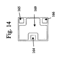
- ground foot pads 161 through 163, a transmission foot pad 164, a reception foot pad 165, and a common terminal foot pad 166 are formed on the lower surface of the line pattern/foot pad layer 124. These foot pads are collectively denoted by reference numeral 129 in Fig. 3 .
- the line patterns and the foot pads shown in Figs. 5D and 5E form the circuit illustrated in Fig. 6 .
- the partition ground line pattern 160 is interposed between the signal line patterns. More specifically, the partition ground line pattern 160 is interposed between the common terminal signal line pattern 146 and the reception signal line pattern 145, between the common terminal signal line pattern 146 and the transmission signal line pattern 144, and between the transmission signal line pattern 144 and the reception signal line pattern 145. Likewise, the partition ground line pattern 160 is interposed between the signal line patterns in the line pattern layer shown in Fig. 5D .
- Fig. 7 is a graph showing the frequency characteristics of the reception filter of the duplexer in accordance with the first embodiment and the reception filter of a conventional duplexer without the partition ground line pattern 160.
- the abscissa axis indicates frequency (MHz), and the ordinate axis indicates insertion loss (dB).
- the solid line indicates the frequency characteristics of the reception filter 113 of the duplexer in accordance with the first embodiment, and the broken line indicates the frequency characteristics of the reception filter of a conventional duplexer.
- the partition ground line pattern 160 is interposed between the reception signal line patterns 145 and 155 and between the common terminal signal line patterns 146 and 156.
- the die-attach layer 123 may be provided with a partition ground line pattern. However, it is necessary to form a large number of line patterns in the die-attach layer 123. Therefore, the size of the die-attach layer 123 needs to be increased so as to accommodate the partition ground line pattern.
- the partition ground line pattern 160 is formed on the upper surface of the line pattern/foot pad layer 124, which is located below the die-attach layer 123. Thus, a smaller duplexer with highly restrained characteristics can be realized.
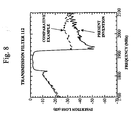
- Fig. 8 is a graph showing the frequency characteristics of the transmission filter of the duplexer in accordance with the first embodiment and the transmission filter of a conventional duplexer without the partition ground line pattern 160.
- the abscissa axis indicates frequency (MHz), and the ordinate axis indicates insertion loss (dB).
- the solid line indicates the frequency characteristics of the transmission filter 112 of the duplexer in accordance with the first embodiment, and the broken line indicates the frequency characteristics of the transmission filter of a conventional duplexer.
- the partition ground line pattern 160 is interposed between the transmission signal line patterns 144 and 154 and between the common terminal signal line patterns 146 and 156. Accordingly, the bridging capacitance between these line patterns can be reduced, and a smaller duplexer with highly restrained characteristics can be realized.
- the inductance that is necessary for the transmission filter 112 is formed with the transmission ground line patterns 141 and 151 formed in the die-attach layer 123 and the line pattern/foot pad layer 124.
- the inductance that is necessary for the reception filter 113 is formed with the reception ground line patterns 142 and 152 formed in the die-attach layer 123 and the line pattern/foot pad layer 124.
- the transmission ground line patterns 141 and 151 connect the ground of the transmission filter 112 directly to the ground foot pad 161.
- the reception ground line patterns 142 and 152 connect the ground of the reception filter 113 directly to the ground foot pads 162 and 163.
- the phase matching circuit ground line pattern 143 connects the ground of the phase matching circuit 130 directly to the ground foot pad 163.
- the partition ground line pattern 160 connects the ground foot pads 161 through 163 to one another. With this arrangement, necessary ground inductances can be obtained, and can be readily controlled. Furthermore, stable filter characteristics that are hardly affected by external noise can be achieved, regardless of the mounting state of the duplexer.
- the partition ground line pattern 160 is interposed between the transmission signal line pattern 154 and the reception foot pad 165 and between the transmission signal line pattern 154 and the common terminal foot pad 166.
- the partition ground line pattern 160 is also interposed between the reception signal line pattern 155 and the transmission foot pad 164 and between the reception signal line pattern 155 and the common terminal foot pad 166.
- the partition ground line pattern 160 is also interposed between the common terminal signal line pattern 156 and the transmission foot pad 164 and the common terminal signal line pattern 156 and the reception foot pad 165.
- the partition ground line pattern 160 is disposed not to overlap with the transmission signal line pattern 144 and the reception signal line pattern 145. With this arrangement, the bridging capacitance between signals can be further reduced, and highly restrained filter characteristics can be realized.
- This arrangement is effective in a case where the base layer 126 of the laminated package 120 is as thin as 0.1 mm. If the signal line patterns overlap with the partition ground line pattern 160 in the case of such a thin base layer, the stray capacitance of the signal line patterns greatly increases, resulting in poor impedance matching and more insertion loss.
- Fig. 9 illustrates the structure of a duplexer as a comparative example.
- This comparative example is a modification of the structure of the first embodiment.
- the partition ground line pattern 160 connects the components other than the ground foot pads 161 through 163.
- the partition ground line pattern 160 connects or integrates the transmission ground line patterns 141 and 151, the reception ground line patterns 142 and 152, and the phase matching circuit ground pattern 143.
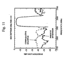
- Fig. 10 shows the frequency characteristics of the transmission filters 112 of the comparative example and the first embodiment.
- Fig. 11 shows the frequency characteristics of the reception filters 113 of the comparative example and the first embodiment.
- the solid line indicates the characteristics of the first embodiment, and the broken line indicates the characteristics of the comparative example.
- Fig. 10 shows the measurement results that were obtained where the partition ground line pattern 160 was not connected to the reception ground line patterns 142 and 152.
- Fig. 11 shows the measurement results that were obtained where the partition ground line pattern 160 was not connected to the transmission ground line patterns 141 and 151.
- the inductance of the partition ground line pattern 160 is greatly reflected in the characteristics, and the stop-band suppression is poor.
- the degree of the stop-band suppression in the first embodiment is high.
- the reception ground line patterns 142 and 152 are connected or integrated to the grounds of the reception filter 113, and are connected to each other with the partition ground line pattern 160 via the ground foot pads 162 and 163.
- the degree of the stop-band suppression of the reception filter 113 can be increased with this structure.
- the broken line in Fig. 12 indicates the characteristics of a comparative example in which the grounds of the reception filter 113 are connected in an inner layer of the laminated package 120.
- the transmission ground line patterns 141 and 151 and the reception ground line patterns 142 and 152 are connected via the ground foot pads 161 through 163, so that the degree of stop-band suppression is increased as shown in Fig. 13 .
- the broken line in Fig. 13 indicates the characteristics of a comparative example in which the transmission ground line patterns 141 and 151 and the reception ground line patterns 142 and 152 are not connected in the laminated package 120.
- the ground foot pads 161 through 163 may be connected as shown in Fig. 14 .
- the laminated package 120 is made of alumina or glass ceramics with relative permittivity of approximately 9.5.
- the phase matching circuit 130 is a lumped-constant circuit that includes an inductor and a capacitor formed on an insulating substrate.
- the outside dimension of the laminated package 120 is approximately 2.5 ⁇ 2 ⁇ 0.6 mm.
- the package size of a conventional duplexer is approximately 5 X 5 ⁇ 1.5 mm or 3.8 ⁇ 3.8 ⁇ 1.5 mm. Compared with this, the duplexer of the present invention is much smaller.
- the filter chip may be a piezoelectric single-crystal substrate of 42° Y-cut X-propagation LiTaO 3 , for example, and a ladder filter (the transmission filter 112) and a multi-mode filter (the reception filter 113) are formed on the piezoelectric single-crystal substrate.
- Fig. 15 illustrates an example of the filter chip.
- the multi-mode filter has a single-port configuration in the structure illustrated in Fig. 15 , it may have a balanced output configuration.
- the transmission filter 112 and the reception filter 113 may also be piezoelectric thin-film resonators.
- Figs. 16A and 16B illustrate an example of a filter (a FBAR filter) that is formed with piezoelectric thin-film resonators (FBAR).
- Fig. 17 shows an example circuit structure of a duplexer that employs the FBAR filter.
- Fig. 16A is a plan view of the FBAR filter
- Fig. 16B is a cross-sectional view of the FBAR filter, taken along the line X-X.
- the first BFBAR filter includes several FBARs. Each FBAR is a structure that has a laminated structure of an upper electrode film 24, a piezoelectric film 23, and a lower electrode film 22.
- cavities 27 formed in a substrate 21 are located immediately below the lower electrode film 22 as opposed to the upper electrode film 24, thereby enclosing elastic energy.
- the lower electrode film 22 may have a two-layer structure, for example.
- the film that is exposed to the cavities 27 may be a Cr film, and the film that is disposed on the Cr film may be a Ru film, for example.
- Two adjusting layers 25 and 26 for adjusting the center frequency of the FBAR filter are formed on the upper electrode film 24.
- the FBAR filter includes four series-arm resonator S1 through S4 and four parallel-arm resonators P1 through P4.
- the parallel-arm resonators P1 through P4 are connected to ground patterns 28 formed on the piezoelectric film 23.
- the two ends of the upper electrode film 24 are used as input/output terminals.
- the duplexer illustrated in Fig. 17 is formed.
- the illustrated duplexer includes FBAR filters 40 and 50 that embody the transmission filter 112 and the reception filter 113, respectively.
- Phase matching circuits 20 and 30 are provided for the FBAR filters 40 and 50, respectively.
- An inductance LP1 is interposed between the ground and the parallel-arm resonators P1 and P2 of the FBAR filter 40, and an inductance LP2 is interposed between the ground and the parallel-arm resonators P3 and P4 of the FBAR filter 40.
- These inductances LP1 and LP2 are embodied by the above described transmission ground line patterns 141 and 151 and the reception ground line patterns 142 and 152.
- the FBAR filter 50 is formed in the same manner as the FBAR filter 40.
- the FBAR filter 50 includes four series-arm resonators S1' through S4', four parallel-arm resonators P1' through P4', and inductances LP1' and LP2'.
- the duplexer with the above described structure in accordance with the present invention constantly exhibits high filter characteristics while maintaining high isolation between signals, despite the small device size.
- Figs. 18A and 18B show a duplexer in accordance with a second embodiment of the present invention.
- the direction of the ground current flowing through the transmission ground line pattern 151 is substantially opposite to the direction of the ground current flowing through the reception ground line pattern 152, as shown in Fig. 18A . Accordingly, the mutual inductance between the grounds can be reduced.
- Fig. 18B shows the filter characteristics of the second embodiment (indicated by the solid line), and the filter characteristics of a comparative example (indicated by the broken line).
- the comparative example has a structure in which the direction of the ground current flowing through the transmission ground line pattern 151 is substantially the same as the direction of the ground current flowing through the reception ground line pattern 152.
- the duplexer in accordance with the second embodiment has a higher degree of stop-band suppression.
Claims (5)
- Duplexer mit:einem Sendefilter (112) und einem Empfangsfilter (113), deren Bandmittenfrequenzen sich voneinander unterscheiden;einer Phasenanpassungsschaltung (130), die eine Phasenanpassung bei dem Sendefilter und dem Empfangsfilter ausführt; undeiner laminierten Packung (12), die eine erste Schicht (123) und eine zweite Schicht (124) enthält, welche zweite Schicht ein erstes Erdungsfußkissen (161) umfasst, das zur externen Verbindung verwendet wird, ein zweites Erdungsfußkissen (162, 163), das zur externen Verbindung verwendet wird, ein Sendesignalfußkissen (164), das zur externen Verbindung verwendet wird, und ein Empfangssignalfußkissen (165), das zur externen Verbindung verwendet wird,
wobei das Sendefilter, das Empfangsfilter und die Phasenanpassungsschaltung auf die erste Schicht montiert sind,die erste Schicht (123) ein erstes Erdungsleitungsmuster (141) enthält, das mit der Erde des Sendefilters (112) verbunden ist, ein zweites Erdungsleitungsmuster (142), das mit der Erde des Empfangsfilters (113) verbunden ist, ein drittes Erdungsleitungsmuster (143), das mit der Erde der Phasenanpassungsschaltung (130) verbunden ist, ein erstes Sendesignalleitungsmuster (144) und ein erstes Empfangssignalleitungsmuster (145),die zweite Schicht (124) unter der ersten Schicht (123) angeordnet ist, die zweite Schicht ein zweites Sendesignalleitungsmuster (154) umfasst, das mit dem Sendefilter (112) über die erste Sendesignalleitung (144) verbunden isL und mit dem Sendesignalfußkissen (164) verbunden ist, ein zweites Empfangssignalleitungsmuster (155), das mit dem Empfangsfilter (113) über das erste Empfangssignalleitungsmuster (145) verbunden ist und mit dem Empfangssignalfußkissen (165) verbunden ist, und ein Partitionserdungsleitungsmuster (160), das zwischen dem zweiten Sendesignalleitungsmuster (154) und dem zweiten Empfangssignalleitungsmuster (155) auf derselben Oberfläche der zweiten Schicht angeordnet ist, die der Oberfläche der zweiten Schicht gegenüberliegt, die die Sendesignal, Empfangssignal- und Erdungsfußkissen enthält,
wobei das erste Erdungsleitungsmuster (141) mit dem Partitionserdungsleitungsmuster (160) nur über das erste Erdungsfußkissen (161) verbunden ist,das zweite Erdungsleitungsmuster (142) mit dem Partitionserdungsleitungsmuster (160) nur über das zweite Erdungsfußkissen (162, 163) verbunden isL. - Duplexer nach Anspruch 1, bei dem das erste Erdungsleitungsmuster (141) mit dem zweiten Erdungsleitungsmuster (142) nicht überlappt ist.
- Duplexer nach Anspruch 1, bei dem das Sendefilter (112) und das Empfangsfilter (113) auf wenigstens einem Chip gebildet sind und mit der Kontaktseite nach unten auf die erste Schicht (123) montiert sind.
- Duplexer nach Anspruch 1, bei dem das Sendefilter (112) und das Empfangsfilter (113) Oberflächenakustikwellenfilter sind.
- Duplexer nach Anspruch 1, bei dem das Sendefilter (112) und das Empfangsfilter (113) piezoelektrische Dünnfilmfilter sind.
Applications Claiming Priority (1)
| Application Number | Priority Date | Filing Date | Title |
|---|---|---|---|
| JP2004371079A JP4091043B2 (ja) | 2004-12-22 | 2004-12-22 | 分波器 |
Publications (3)
| Publication Number | Publication Date |
|---|---|
| EP1675262A2 EP1675262A2 (de) | 2006-06-28 |
| EP1675262A3 EP1675262A3 (de) | 2007-09-12 |
| EP1675262B1 true EP1675262B1 (de) | 2010-03-10 |
Family
ID=35985235
Family Applications (1)
| Application Number | Title | Priority Date | Filing Date |
|---|---|---|---|
| EP05257144A Expired - Fee Related EP1675262B1 (de) | 2004-12-22 | 2005-11-21 | Duplexer |
Country Status (6)
| Country | Link |
|---|---|
| US (1) | US7579927B2 (de) |
| EP (1) | EP1675262B1 (de) |
| JP (1) | JP4091043B2 (de) |
| KR (1) | KR100742911B1 (de) |
| CN (1) | CN1812260B (de) |
| DE (1) | DE602005019840D1 (de) |
Families Citing this family (22)
| Publication number | Priority date | Publication date | Assignee | Title |
|---|---|---|---|---|
| KR100777451B1 (ko) * | 2006-10-31 | 2007-11-21 | 삼성전자주식회사 | 박막 벌크 음향 공진기 필터 및 듀플렉서 |
| JP5041285B2 (ja) * | 2007-04-24 | 2012-10-03 | 日立金属株式会社 | 高周波部品 |
| DE102007019325B4 (de) * | 2007-04-24 | 2008-12-24 | Epcos Ag | Mit akustischen Wellen arbeitendes Bauelement |
| CN101682313B (zh) | 2007-05-28 | 2012-09-26 | 株式会社村田制作所 | 双工器及弹性波装置 |
| WO2009025056A1 (ja) * | 2007-08-23 | 2009-02-26 | Fujitsu Limited | デュープレクサ、通信モジュール、および通信装置 |
| JP5344736B2 (ja) | 2008-02-20 | 2013-11-20 | 太陽誘電株式会社 | 基材、通信モジュール、および通信装置 |
| CN101953070B (zh) | 2008-02-20 | 2015-03-25 | 太阳诱电株式会社 | 滤波器、分波器、通信模块以及通信装置 |
| DE102008045346B4 (de) | 2008-09-01 | 2018-06-07 | Snaptrack Inc. | Duplexer und Verfahren zum Erhöhen der Isolation zwischen zwei Filtern |
| JP4663770B2 (ja) * | 2008-09-29 | 2011-04-06 | 太陽誘電株式会社 | 弾性波デバイス |
| KR20110113340A (ko) | 2010-04-09 | 2011-10-17 | 한국전자통신연구원 | Crlh 구조 공진기 기반의 대역 통과 필터 및 이를 이용한 듀플렉서 |
| JP5603209B2 (ja) | 2010-11-10 | 2014-10-08 | 太陽誘電株式会社 | 分波器及びこれを備えた電子装置 |
| JP5653187B2 (ja) | 2010-11-18 | 2015-01-14 | 太陽誘電株式会社 | 分波器 |
| US9685950B2 (en) | 2011-03-23 | 2017-06-20 | Shenzhen Ada Electronics Co., Ltd. | Energy-saving electronic touch switch |
| WO2012144229A1 (ja) | 2011-04-22 | 2012-10-26 | 株式会社村田製作所 | 分波器およびこれを備える回路モジュール |
| JP6074167B2 (ja) * | 2012-06-12 | 2017-02-01 | 太陽誘電株式会社 | フィルタモジュール及び分波器モジュール |
| CN103248334A (zh) * | 2013-05-08 | 2013-08-14 | 天津大学 | 压电声波谐振器和滤波器 |
| JP2016012796A (ja) * | 2014-06-27 | 2016-01-21 | 太陽誘電株式会社 | フィルタ、デュプレクサおよびモジュール。 |
| KR101942731B1 (ko) * | 2017-04-10 | 2019-01-28 | 삼성전기 주식회사 | 필터 및 필터 모듈 |
| WO2018212105A1 (ja) * | 2017-05-15 | 2018-11-22 | 株式会社村田製作所 | マルチプレクサ、送信装置および受信装置 |
| KR102561938B1 (ko) * | 2020-10-27 | 2023-08-01 | 삼성전기주식회사 | 탄성파 필터 장치 |
| WO2023112652A1 (ja) * | 2021-12-15 | 2023-06-22 | 株式会社村田製作所 | 弾性波装置 |
| CN116032246B (zh) * | 2023-03-27 | 2023-10-31 | 成都频岢微电子有限公司 | 一种双工器 |
Citations (1)
| Publication number | Priority date | Publication date | Assignee | Title |
|---|---|---|---|---|
| US20040212451A1 (en) * | 2003-04-28 | 2004-10-28 | Fujitsu Media Devices Limited | Duplexer using surface acoustic wave filters |
Family Cites Families (17)
| Publication number | Priority date | Publication date | Assignee | Title |
|---|---|---|---|---|
| US4847379A (en) | 1987-11-30 | 1989-07-11 | E. R. Squibb & Sons, Inc. | 3,6-dihydro-1,5(2H)-pyrimidinecarboxylic acid esters |
| JP3487692B2 (ja) * | 1995-10-02 | 2004-01-19 | 富士通株式会社 | 分波器 |
| JPH11186872A (ja) * | 1997-12-25 | 1999-07-09 | Oki Business Co Ltd | 分波器多層基板パッケージ |
| EP1154571A4 (de) * | 1999-12-24 | 2005-09-14 | Matsushita Electric Ind Co Ltd | Antennenduplexer |
| JP2001313542A (ja) | 2000-04-28 | 2001-11-09 | Oki Electric Ind Co Ltd | 分波器 |
| DE10138335B4 (de) * | 2000-07-28 | 2010-10-21 | Kyocera Corp. | Oberflächenwellen-Bauteil |
| KR100384399B1 (ko) | 2000-11-28 | 2003-05-22 | 주식회사 케이이씨 | 듀플렉서의 주파수 격리회로 |
| US6462631B2 (en) * | 2001-02-14 | 2002-10-08 | Agilent Technologies, Inc. | Passband filter having an asymmetrical filter response |
| JP3818896B2 (ja) * | 2001-11-26 | 2006-09-06 | 富士通メディアデバイス株式会社 | 分波器及びこれを用いた電子装置 |
| JP2004080233A (ja) * | 2002-08-14 | 2004-03-11 | Murata Mfg Co Ltd | 分波器 |
| JP2004120295A (ja) | 2002-09-26 | 2004-04-15 | Kyocera Corp | デュプレクサ |
| KR100541077B1 (ko) * | 2003-05-14 | 2006-01-10 | 삼성전기주식회사 | 정합회로 및 그 정합회로를 포함하는 적층형 듀플렉서 |
| US6822537B1 (en) * | 2003-05-14 | 2004-11-23 | Murata Manufacturing Co., Ltd. | Surface acoustic wave branching filter |
| KR100500391B1 (ko) * | 2003-05-20 | 2005-07-18 | 전자부품연구원 | 박막형 체적 탄성 공진기 필터를 사용한 듀플렉싱 모듈 |
| JP4525594B2 (ja) * | 2003-07-29 | 2010-08-18 | パナソニック株式会社 | 弾性表面波デバイス |
| US7385463B2 (en) * | 2003-12-24 | 2008-06-10 | Kyocera Corporation | Surface acoustic wave device and electronic circuit device |
| KR20050081738A (ko) * | 2004-02-16 | 2005-08-19 | 엘지이노텍 주식회사 | 듀플렉서 및 듀플렉서 패키지 |
-
2004
- 2004-12-22 JP JP2004371079A patent/JP4091043B2/ja not_active Expired - Fee Related
-
2005
- 2005-11-21 EP EP05257144A patent/EP1675262B1/de not_active Expired - Fee Related
- 2005-11-21 DE DE602005019840T patent/DE602005019840D1/de active Active
- 2005-12-02 US US11/291,775 patent/US7579927B2/en active Active
- 2005-12-21 KR KR1020050126846A patent/KR100742911B1/ko active IP Right Grant
- 2005-12-22 CN CN2005101321763A patent/CN1812260B/zh active Active
Patent Citations (1)
| Publication number | Priority date | Publication date | Assignee | Title |
|---|---|---|---|---|
| US20040212451A1 (en) * | 2003-04-28 | 2004-10-28 | Fujitsu Media Devices Limited | Duplexer using surface acoustic wave filters |
Also Published As
| Publication number | Publication date |
|---|---|
| CN1812260B (zh) | 2011-08-03 |
| EP1675262A2 (de) | 2006-06-28 |
| DE602005019840D1 (de) | 2010-04-22 |
| CN1812260A (zh) | 2006-08-02 |
| JP2006180192A (ja) | 2006-07-06 |
| EP1675262A3 (de) | 2007-09-12 |
| US7579927B2 (en) | 2009-08-25 |
| KR20060072062A (ko) | 2006-06-27 |
| KR100742911B1 (ko) | 2007-07-25 |
| US20060132260A1 (en) | 2006-06-22 |
| JP4091043B2 (ja) | 2008-05-28 |
Similar Documents
| Publication | Publication Date | Title |
|---|---|---|
| EP1675262B1 (de) | Duplexer | |
| US6943645B2 (en) | Surface acoustic wave duplexer and communication apparatus having the same | |
| US6756864B2 (en) | Branching filter and communication apparatus | |
| US7941103B2 (en) | Duplexer | |
| KR100717659B1 (ko) | 분파기 및 전자 장치 | |
| KR100733101B1 (ko) | 분파기 | |
| US7084718B2 (en) | Band elimination filter, filter device, antenna duplexer and communication apparatus | |
| US7479846B2 (en) | Duplexer | |
| US7276992B2 (en) | Antenna duplexer and electronic device | |
| US7629863B2 (en) | Filter and duplexer | |
| US20060139125A1 (en) | Filter device | |
| CN1852026B (zh) | 滤波器和双工器 | |
| JP3967289B2 (ja) | 分波器及び電子装置 | |
| JP2003115748A (ja) | 弾性表面波分波器、通信装置 | |
| JP4207836B2 (ja) | 弾性表面波分波器 | |
| JP2002198774A (ja) | 複合電子部品 | |
| JP2002300006A (ja) | 高周波部品及びアンテナ共用器 |
Legal Events
| Date | Code | Title | Description |
|---|---|---|---|
| PUAI | Public reference made under article 153(3) epc to a published international application that has entered the european phase |
Free format text: ORIGINAL CODE: 0009012 |
|
| AK | Designated contracting states |
Kind code of ref document: A2 Designated state(s): AT BE BG CH CY CZ DE DK EE ES FI FR GB GR HU IE IS IT LI LT LU LV MC NL PL PT RO SE SI SK TR |
|
| AX | Request for extension of the european patent |
Extension state: AL BA HR MK YU |
|
| PUAL | Search report despatched |
Free format text: ORIGINAL CODE: 0009013 |
|
| AK | Designated contracting states |
Kind code of ref document: A3 Designated state(s): AT BE BG CH CY CZ DE DK EE ES FI FR GB GR HU IE IS IT LI LT LU LV MC NL PL PT RO SE SI SK TR |
|
| AX | Request for extension of the european patent |
Extension state: AL BA HR MK YU |
|
| 17P | Request for examination filed |
Effective date: 20071107 |
|
| 17Q | First examination report despatched |
Effective date: 20071214 |
|
| AKX | Designation fees paid |
Designated state(s): DE FR GB |
|
| GRAP | Despatch of communication of intention to grant a patent |
Free format text: ORIGINAL CODE: EPIDOSNIGR1 |
|
| GRAS | Grant fee paid |
Free format text: ORIGINAL CODE: EPIDOSNIGR3 |
|
| GRAA | (expected) grant |
Free format text: ORIGINAL CODE: 0009210 |
|
| AK | Designated contracting states |
Kind code of ref document: B1 Designated state(s): DE FR GB |
|
| REG | Reference to a national code |
Ref country code: GB Ref legal event code: FG4D |
|
| REF | Corresponds to: |
Ref document number: 602005019840 Country of ref document: DE Date of ref document: 20100422 Kind code of ref document: P |
|
| REG | Reference to a national code |
Ref country code: GB Ref legal event code: 732E Free format text: REGISTERED BETWEEN 20100610 AND 20100616 |
|
| RAP2 | Party data changed (patent owner data changed or rights of a patent transferred) |
Owner name: TAIYO YUDEN CO., LTD. Owner name: FUJITSU MEDIA DEVICES LIMITED |
|
| REG | Reference to a national code |
Ref country code: FR Ref legal event code: TP |
|
| RAP2 | Party data changed (patent owner data changed or rights of a patent transferred) |
Owner name: TAIYO YUDEN CO., LTD. |
|
| REG | Reference to a national code |
Ref country code: FR Ref legal event code: TQ Ref country code: FR Ref legal event code: TP |
|
| REG | Reference to a national code |
Ref country code: GB Ref legal event code: 732E Free format text: REGISTERED BETWEEN 20101202 AND 20101208 |
|
| REG | Reference to a national code |
Ref country code: GB Ref legal event code: 732E Free format text: REGISTERED BETWEEN 20101209 AND 20101215 |
|
| PLBE | No opposition filed within time limit |
Free format text: ORIGINAL CODE: 0009261 |
|
| STAA | Information on the status of an ep patent application or granted ep patent |
Free format text: STATUS: NO OPPOSITION FILED WITHIN TIME LIMIT |
|
| PGFP | Annual fee paid to national office [announced via postgrant information from national office to epo] |
Ref country code: FR Payment date: 20101130 Year of fee payment: 6 |
|
| 26N | No opposition filed |
Effective date: 20101213 |
|
| PGFP | Annual fee paid to national office [announced via postgrant information from national office to epo] |
Ref country code: GB Payment date: 20101118 Year of fee payment: 6 |
|
| REG | Reference to a national code |
Ref country code: DE Ref legal event code: R081 Ref document number: 602005019840 Country of ref document: DE Owner name: TAIYO YUDEN CO., LTD., JP Free format text: FORMER OWNER: FUJITSU MEDIA DEVICES LIMITED, TAIYO YUDEN CO., LTD., , JP Effective date: 20110310 Ref country code: DE Ref legal event code: R081 Ref document number: 602005019840 Country of ref document: DE Owner name: TAIYO YUDEN CO., LTD., JP Free format text: FORMER OWNERS: FUJITSU MEDIA DEVICES LIMITED, YOKOHAMA-SHI, KANAGAWA, JP; TAIYO YUDEN CO., LTD., TOKIO/TOKYO, JP Effective date: 20110310 |
|
| GBPC | Gb: european patent ceased through non-payment of renewal fee |
Effective date: 20111121 |
|
| REG | Reference to a national code |
Ref country code: FR Ref legal event code: ST Effective date: 20120731 |
|
| PG25 | Lapsed in a contracting state [announced via postgrant information from national office to epo] |
Ref country code: GB Free format text: LAPSE BECAUSE OF NON-PAYMENT OF DUE FEES Effective date: 20111121 |
|
| PG25 | Lapsed in a contracting state [announced via postgrant information from national office to epo] |
Ref country code: FR Free format text: LAPSE BECAUSE OF NON-PAYMENT OF DUE FEES Effective date: 20111130 |
|
| PGFP | Annual fee paid to national office [announced via postgrant information from national office to epo] |
Ref country code: DE Payment date: 20121121 Year of fee payment: 8 |
|
| REG | Reference to a national code |
Ref country code: DE Ref legal event code: R119 Ref document number: 602005019840 Country of ref document: DE Effective date: 20140603 |
|
| PG25 | Lapsed in a contracting state [announced via postgrant information from national office to epo] |
Ref country code: DE Free format text: LAPSE BECAUSE OF NON-PAYMENT OF DUE FEES Effective date: 20140603 |