EP1584705B1 - Source de vapeur pour dispositif de revêtement. - Google Patents
Source de vapeur pour dispositif de revêtement. Download PDFInfo
- Publication number
- EP1584705B1 EP1584705B1 EP05004709A EP05004709A EP1584705B1 EP 1584705 B1 EP1584705 B1 EP 1584705B1 EP 05004709 A EP05004709 A EP 05004709A EP 05004709 A EP05004709 A EP 05004709A EP 1584705 B1 EP1584705 B1 EP 1584705B1
- Authority
- EP
- European Patent Office
- Prior art keywords
- film formation
- discharge
- passage
- discharge passage
- escape
- Prior art date
- Legal status (The legal status is an assumption and is not a legal conclusion. Google has not performed a legal analysis and makes no representation as to the accuracy of the status listed.)
- Expired - Fee Related
Links
- 230000015572 biosynthetic process Effects 0.000 title claims description 319
- 239000000463 material Substances 0.000 claims description 259
- 239000000758 substrate Substances 0.000 claims description 42
- 238000000034 method Methods 0.000 claims description 38
- 238000010438 heat treatment Methods 0.000 claims description 37
- 238000004519 manufacturing process Methods 0.000 claims description 18
- 238000001514 detection method Methods 0.000 claims description 13
- 239000011368 organic material Substances 0.000 claims description 10
- 238000007599 discharging Methods 0.000 claims description 3
- 238000005755 formation reaction Methods 0.000 description 272
- 239000010410 layer Substances 0.000 description 41
- 229910052751 metal Inorganic materials 0.000 description 11
- 239000002184 metal Substances 0.000 description 11
- 230000008569 process Effects 0.000 description 11
- 238000007740 vapor deposition Methods 0.000 description 10
- -1 polyphenylene vinylene Polymers 0.000 description 9
- 230000000694 effects Effects 0.000 description 7
- 239000012044 organic layer Substances 0.000 description 7
- 238000009877 rendering Methods 0.000 description 6
- 239000002274 desiccant Substances 0.000 description 5
- 238000007789 sealing Methods 0.000 description 5
- LTPBRCUWZOMYOC-UHFFFAOYSA-N Beryllium oxide Chemical compound O=[Be] LTPBRCUWZOMYOC-UHFFFAOYSA-N 0.000 description 4
- 239000000956 alloy Substances 0.000 description 4
- 229910045601 alloy Inorganic materials 0.000 description 4
- 230000006866 deterioration Effects 0.000 description 4
- PXHVJJICTQNCMI-UHFFFAOYSA-N Nickel Chemical compound [Ni] PXHVJJICTQNCMI-UHFFFAOYSA-N 0.000 description 3
- YXFVVABEGXRONW-UHFFFAOYSA-N Toluene Chemical compound CC1=CC=CC=C1 YXFVVABEGXRONW-UHFFFAOYSA-N 0.000 description 3
- 239000000853 adhesive Substances 0.000 description 3
- 239000012298 atmosphere Substances 0.000 description 3
- 230000000903 blocking effect Effects 0.000 description 3
- 230000008859 change Effects 0.000 description 3
- 239000011651 chromium Substances 0.000 description 3
- 239000003822 epoxy resin Substances 0.000 description 3
- 230000008020 evaporation Effects 0.000 description 3
- 238000001704 evaporation Methods 0.000 description 3
- 150000004767 nitrides Chemical class 0.000 description 3
- BASFCYQUMIYNBI-UHFFFAOYSA-N platinum Chemical compound [Pt] BASFCYQUMIYNBI-UHFFFAOYSA-N 0.000 description 3
- 229920000647 polyepoxide Polymers 0.000 description 3
- 238000011084 recovery Methods 0.000 description 3
- 229920005989 resin Polymers 0.000 description 3
- 239000011347 resin Substances 0.000 description 3
- 230000004044 response Effects 0.000 description 3
- 230000001502 supplementing effect Effects 0.000 description 3
- 238000001771 vacuum deposition Methods 0.000 description 3
- OKTJSMMVPCPJKN-UHFFFAOYSA-N Carbon Chemical compound [C] OKTJSMMVPCPJKN-UHFFFAOYSA-N 0.000 description 2
- RTZKZFJDLAIYFH-UHFFFAOYSA-N Diethyl ether Chemical compound CCOCC RTZKZFJDLAIYFH-UHFFFAOYSA-N 0.000 description 2
- ZOKXTWBITQBERF-UHFFFAOYSA-N Molybdenum Chemical compound [Mo] ZOKXTWBITQBERF-UHFFFAOYSA-N 0.000 description 2
- URLKBWYHVLBVBO-UHFFFAOYSA-N Para-Xylene Chemical group CC1=CC=C(C)C=C1 URLKBWYHVLBVBO-UHFFFAOYSA-N 0.000 description 2
- 239000012790 adhesive layer Substances 0.000 description 2
- 239000002585 base Substances 0.000 description 2
- 239000011247 coating layer Substances 0.000 description 2
- 150000001875 compounds Chemical class 0.000 description 2
- 230000007423 decrease Effects 0.000 description 2
- QDOXWKRWXJOMAK-UHFFFAOYSA-N dichromium trioxide Chemical compound O=[Cr]O[Cr]=O QDOXWKRWXJOMAK-UHFFFAOYSA-N 0.000 description 2
- 230000005281 excited state Effects 0.000 description 2
- 239000005357 flat glass Substances 0.000 description 2
- 239000011521 glass Substances 0.000 description 2
- 238000002347 injection Methods 0.000 description 2
- 239000007924 injection Substances 0.000 description 2
- 229910010272 inorganic material Inorganic materials 0.000 description 2
- 239000011147 inorganic material Substances 0.000 description 2
- 239000012212 insulator Substances 0.000 description 2
- 238000010030 laminating Methods 0.000 description 2
- 238000004020 luminiscence type Methods 0.000 description 2
- 238000002844 melting Methods 0.000 description 2
- 229910052750 molybdenum Inorganic materials 0.000 description 2
- 239000011733 molybdenum Substances 0.000 description 2
- 150000002894 organic compounds Chemical class 0.000 description 2
- 239000004033 plastic Substances 0.000 description 2
- 229920003023 plastic Polymers 0.000 description 2
- 239000000047 product Substances 0.000 description 2
- 230000002035 prolonged effect Effects 0.000 description 2
- 239000002356 single layer Substances 0.000 description 2
- ZAMOUSCENKQFHK-UHFFFAOYSA-N Chlorine atom Chemical compound [Cl] ZAMOUSCENKQFHK-UHFFFAOYSA-N 0.000 description 1
- VYZAMTAEIAYCRO-UHFFFAOYSA-N Chromium Chemical compound [Cr] VYZAMTAEIAYCRO-UHFFFAOYSA-N 0.000 description 1
- YCKRFDGAMUMZLT-UHFFFAOYSA-N Fluorine atom Chemical compound [F] YCKRFDGAMUMZLT-UHFFFAOYSA-N 0.000 description 1
- CTQNGGLPUBDAKN-UHFFFAOYSA-N O-Xylene Chemical compound CC1=CC=CC=C1C CTQNGGLPUBDAKN-UHFFFAOYSA-N 0.000 description 1
- 239000004698 Polyethylene Substances 0.000 description 1
- 239000004642 Polyimide Substances 0.000 description 1
- VYPSYNLAJGMNEJ-UHFFFAOYSA-N Silicium dioxide Chemical compound O=[Si]=O VYPSYNLAJGMNEJ-UHFFFAOYSA-N 0.000 description 1
- XUIMIQQOPSSXEZ-UHFFFAOYSA-N Silicon Chemical compound [Si] XUIMIQQOPSSXEZ-UHFFFAOYSA-N 0.000 description 1
- 229910021536 Zeolite Inorganic materials 0.000 description 1
- 125000001931 aliphatic group Chemical group 0.000 description 1
- 229910052783 alkali metal Inorganic materials 0.000 description 1
- 229910000272 alkali metal oxide Inorganic materials 0.000 description 1
- 150000001340 alkali metals Chemical class 0.000 description 1
- 229910052784 alkaline earth metal Inorganic materials 0.000 description 1
- 150000001342 alkaline earth metals Chemical class 0.000 description 1
- 150000004703 alkoxides Chemical class 0.000 description 1
- PNEYBMLMFCGWSK-UHFFFAOYSA-N aluminium oxide Inorganic materials [O-2].[O-2].[O-2].[Al+3].[Al+3] PNEYBMLMFCGWSK-UHFFFAOYSA-N 0.000 description 1
- 229910052788 barium Inorganic materials 0.000 description 1
- 229910052790 beryllium Inorganic materials 0.000 description 1
- 239000011230 binding agent Substances 0.000 description 1
- 238000005422 blasting Methods 0.000 description 1
- 229910052792 caesium Inorganic materials 0.000 description 1
- 229910052791 calcium Inorganic materials 0.000 description 1
- 229910052799 carbon Inorganic materials 0.000 description 1
- 239000002041 carbon nanotube Substances 0.000 description 1
- 229910021393 carbon nanotube Inorganic materials 0.000 description 1
- 238000006243 chemical reaction Methods 0.000 description 1
- 229910052801 chlorine Inorganic materials 0.000 description 1
- 239000000460 chlorine Substances 0.000 description 1
- 229910052804 chromium Inorganic materials 0.000 description 1
- 239000011248 coating agent Substances 0.000 description 1
- 238000000576 coating method Methods 0.000 description 1
- 239000003086 colorant Substances 0.000 description 1
- 238000001816 cooling Methods 0.000 description 1
- 238000000354 decomposition reaction Methods 0.000 description 1
- 230000003247 decreasing effect Effects 0.000 description 1
- 238000000151 deposition Methods 0.000 description 1
- 230000008021 deposition Effects 0.000 description 1
- HNPSIPDUKPIQMN-UHFFFAOYSA-N dioxosilane;oxo(oxoalumanyloxy)alumane Chemical compound O=[Si]=O.O=[Al]O[Al]=O HNPSIPDUKPIQMN-UHFFFAOYSA-N 0.000 description 1
- 239000007772 electrode material Substances 0.000 description 1
- 238000010894 electron beam technology Methods 0.000 description 1
- 238000005530 etching Methods 0.000 description 1
- 229910052731 fluorine Inorganic materials 0.000 description 1
- 239000011737 fluorine Substances 0.000 description 1
- 150000002222 fluorine compounds Chemical class 0.000 description 1
- 238000005286 illumination Methods 0.000 description 1
- 230000002401 inhibitory effect Effects 0.000 description 1
- 238000003475 lamination Methods 0.000 description 1
- 238000004093 laser heating Methods 0.000 description 1
- 239000007788 liquid Substances 0.000 description 1
- 229910052744 lithium Inorganic materials 0.000 description 1
- 229910052749 magnesium Inorganic materials 0.000 description 1
- 230000007246 mechanism Effects 0.000 description 1
- 230000008018 melting Effects 0.000 description 1
- 229910044991 metal oxide Inorganic materials 0.000 description 1
- 150000004706 metal oxides Chemical class 0.000 description 1
- 239000000203 mixture Substances 0.000 description 1
- 230000004048 modification Effects 0.000 description 1
- 238000012986 modification Methods 0.000 description 1
- 238000012806 monitoring device Methods 0.000 description 1
- 229910052759 nickel Inorganic materials 0.000 description 1
- JRZJOMJEPLMPRA-UHFFFAOYSA-N olefin Natural products CCCCCCCC=C JRZJOMJEPLMPRA-UHFFFAOYSA-N 0.000 description 1
- 239000003960 organic solvent Substances 0.000 description 1
- 238000010422 painting Methods 0.000 description 1
- SWELZOZIOHGSPA-UHFFFAOYSA-N palladium silver Chemical compound [Pd].[Ag] SWELZOZIOHGSPA-UHFFFAOYSA-N 0.000 description 1
- 239000002245 particle Substances 0.000 description 1
- 150000002978 peroxides Chemical class 0.000 description 1
- 125000002080 perylenyl group Chemical group C1(=CC=C2C=CC=C3C4=CC=CC5=CC=CC(C1=C23)=C45)* 0.000 description 1
- CSHWQDPOILHKBI-UHFFFAOYSA-N peryrene Natural products C1=CC(C2=CC=CC=3C2=C2C=CC=3)=C3C2=CC=CC3=C1 CSHWQDPOILHKBI-UHFFFAOYSA-N 0.000 description 1
- 239000003208 petroleum Substances 0.000 description 1
- 229910052697 platinum Inorganic materials 0.000 description 1
- 229920000553 poly(phenylenevinylene) Polymers 0.000 description 1
- 229920000767 polyaniline Polymers 0.000 description 1
- 229920000728 polyester Polymers 0.000 description 1
- 229920000573 polyethylene Polymers 0.000 description 1
- 229920001721 polyimide Polymers 0.000 description 1
- 229920001195 polyisoprene Polymers 0.000 description 1
- 229920000098 polyolefin Polymers 0.000 description 1
- 229910052700 potassium Inorganic materials 0.000 description 1
- 239000002243 precursor Substances 0.000 description 1
- 238000003825 pressing Methods 0.000 description 1
- 229910052761 rare earth metal Inorganic materials 0.000 description 1
- 150000002910 rare earth metals Chemical class 0.000 description 1
- 230000009467 reduction Effects 0.000 description 1
- 230000000630 rising effect Effects 0.000 description 1
- 229910052701 rubidium Inorganic materials 0.000 description 1
- 239000004065 semiconductor Substances 0.000 description 1
- 229910002027 silica gel Inorganic materials 0.000 description 1
- 239000000741 silica gel Substances 0.000 description 1
- 229910052710 silicon Inorganic materials 0.000 description 1
- 239000010703 silicon Substances 0.000 description 1
- 229910052814 silicon oxide Inorganic materials 0.000 description 1
- 239000004447 silicone coating Substances 0.000 description 1
- 229910052708 sodium Inorganic materials 0.000 description 1
- 239000011343 solid material Substances 0.000 description 1
- 239000002904 solvent Substances 0.000 description 1
- 125000006850 spacer group Chemical group 0.000 description 1
- 229910052712 strontium Inorganic materials 0.000 description 1
- 238000000859 sublimation Methods 0.000 description 1
- 230000008022 sublimation Effects 0.000 description 1
- 239000000126 substance Substances 0.000 description 1
- 239000013589 supplement Substances 0.000 description 1
- 229910052715 tantalum Inorganic materials 0.000 description 1
- GUVRBAGPIYLISA-UHFFFAOYSA-N tantalum atom Chemical compound [Ta] GUVRBAGPIYLISA-UHFFFAOYSA-N 0.000 description 1
- PBCFLUZVCVVTBY-UHFFFAOYSA-N tantalum pentoxide Inorganic materials O=[Ta](=O)O[Ta](=O)=O PBCFLUZVCVVTBY-UHFFFAOYSA-N 0.000 description 1
- 239000012780 transparent material Substances 0.000 description 1
- WFKWXMTUELFFGS-UHFFFAOYSA-N tungsten Chemical compound [W] WFKWXMTUELFFGS-UHFFFAOYSA-N 0.000 description 1
- 229910052721 tungsten Inorganic materials 0.000 description 1
- 239000010937 tungsten Substances 0.000 description 1
- 229920002554 vinyl polymer Polymers 0.000 description 1
- 239000008096 xylene Substances 0.000 description 1
- 239000010457 zeolite Substances 0.000 description 1
Images



Classifications
-
- C—CHEMISTRY; METALLURGY
- C23—COATING METALLIC MATERIAL; COATING MATERIAL WITH METALLIC MATERIAL; CHEMICAL SURFACE TREATMENT; DIFFUSION TREATMENT OF METALLIC MATERIAL; COATING BY VACUUM EVAPORATION, BY SPUTTERING, BY ION IMPLANTATION OR BY CHEMICAL VAPOUR DEPOSITION, IN GENERAL; INHIBITING CORROSION OF METALLIC MATERIAL OR INCRUSTATION IN GENERAL
- C23C—COATING METALLIC MATERIAL; COATING MATERIAL WITH METALLIC MATERIAL; SURFACE TREATMENT OF METALLIC MATERIAL BY DIFFUSION INTO THE SURFACE, BY CHEMICAL CONVERSION OR SUBSTITUTION; COATING BY VACUUM EVAPORATION, BY SPUTTERING, BY ION IMPLANTATION OR BY CHEMICAL VAPOUR DEPOSITION, IN GENERAL
- C23C14/00—Coating by vacuum evaporation, by sputtering or by ion implantation of the coating forming material
- C23C14/22—Coating by vacuum evaporation, by sputtering or by ion implantation of the coating forming material characterised by the process of coating
- C23C14/24—Vacuum evaporation
-
- C—CHEMISTRY; METALLURGY
- C23—COATING METALLIC MATERIAL; COATING MATERIAL WITH METALLIC MATERIAL; CHEMICAL SURFACE TREATMENT; DIFFUSION TREATMENT OF METALLIC MATERIAL; COATING BY VACUUM EVAPORATION, BY SPUTTERING, BY ION IMPLANTATION OR BY CHEMICAL VAPOUR DEPOSITION, IN GENERAL; INHIBITING CORROSION OF METALLIC MATERIAL OR INCRUSTATION IN GENERAL
- C23C—COATING METALLIC MATERIAL; COATING MATERIAL WITH METALLIC MATERIAL; SURFACE TREATMENT OF METALLIC MATERIAL BY DIFFUSION INTO THE SURFACE, BY CHEMICAL CONVERSION OR SUBSTITUTION; COATING BY VACUUM EVAPORATION, BY SPUTTERING, BY ION IMPLANTATION OR BY CHEMICAL VAPOUR DEPOSITION, IN GENERAL
- C23C14/00—Coating by vacuum evaporation, by sputtering or by ion implantation of the coating forming material
- C23C14/22—Coating by vacuum evaporation, by sputtering or by ion implantation of the coating forming material characterised by the process of coating
- C23C14/54—Controlling or regulating the coating process
- C23C14/542—Controlling the film thickness or evaporation rate
- C23C14/545—Controlling the film thickness or evaporation rate using measurement on deposited material
Definitions
- the present invention relates to a film formation source, a film formation apparatus, a film formation method, an organic EL panel, and a method of manufacturing the organic EL panel.
- a film formationapparatus for forming a filmof a solidmaterial on a substrate is usually equipped with a film formation source containing a film formation material and located within a film formation chamber kept at a vacuum or depressurized state.
- a film formation apparatus may be a vacuum vapor deposition apparatus which heats a vapor deposition source positioned within a vacuum chamber, so that a depositionmaterial discharged from an evaporation outlet of the vapor deposition source can be formed into a film on a substrate disposed within the vacuum chamber.
- an organic EL panel manufacturing method which has drawn considerable attentions in the field of display or illumination, includes a step of forming a first electrode on a substrate, a step of forming thereon an organic material layer consisting of organic compounds, followed by forming thereon a second electrode.
- a step of forming a first electrode on a substrate a step of forming thereon an organic material layer consisting of organic compounds, followed by forming thereon a second electrode.
- each organic EL device serving as an essential element for an organic EL panel contains an organic material layer formed by a plurality of films having different functions.
- an organic EL panel for multi-color displaying is formed in such a manner that organic EL devices consisting of different luminescent materials are formed on a substrate, so that it is necessary to perform film formation of different materials on a single substrate.
- the above-described film formation apparatus or film formation source have been found difficult to carry out film formation of different materials in one chamber, it is necessary to employ a plurality of chambers, hence resulting in an enlarged scale of film formation apparatus and a complex manufacturing process.
- Japanese Unexamined Patent Application Publication No. 2003-317957 has disclosed an improved vapor deposition apparatus in which one or more detachable vapor deposition sources are disposed outside a film formation chamber, a steam distributor having evaporation outlets is disposed within the chamber, a steam transporting system including valves is connected between each vapor deposition source and the steam distributor.
- the aforementioned prior art provides valve in material transport system for transporting the film formation material, thereby adjusting the discharge state by adjusting an opening degree of the valve.
- the valve is provided in an airtight transport system which directs a film formation material (which is produced from a film formation source located outside the film formation chamber) to a discharge outlet of the film formation chamber, since the sublimation or evaporation of the film formation material is difficult to be decelerated at once even if the opening degree of valve is narrowed and a heating velocity is reduced, a reduction in the opening degree of the valve can increase an internal pressure of the film formation chamber.
- the material contained in the film formation source will be undesirably modified due to its decomposition or the like, rendering it impossible to effect an acceptable film formation.
- an operation pressure will go beyond a controllable range, making it impossible to perform an acceptable discharge rate control.
- valve when valve is used to control the discharge state of the film formation material, the film formation material contained within the film formation source will get deteriorated in its quality, an operation pressure will go beyond a controllable pressure range, hence rendering it impossible to perform an acceptable film formation.
- the film formation material is usually continued to be discharged until the material is used up, and the film formation source is then replaced by a new film formation source at the time the material has become zero.
- it is impossible to ensure a desired discharge state and the film formation process has to be stopped temporally before and after the exchange of the film formation source it is impossible to continuously perform the film formation operation while at the same time maintaining a desired film formation state (even if it is possible to exchange the film formation source) for a long time.
- the present invention is to solve the above-discussed problem, and it is an object of the invention to perform a film formation process capable of producing an acceptable film, avoiding a deterioration of a film formation material when supplementing or exchanging the same, controlling the discharge state of the film formation material, improving the productivity of an organic EL panel manufacturing process, and improving product yield by improving film formation precision.
- the present invention is characterized by at least the following aspects.
- a film formation apparatus having a film formation chamber in which a vacuum or a depressurized state is formed and a sublimated or evaporated film formation material is formed into a film on a substrate
- such film formation apparatus comprising: a discharge outlet disposed within the film formation chamber for discharging the film formation material towards a film formation surface of the substrate; a material accommodating section disposed outside the film formation chamber and including a material container containing the film formation material; a heating device for heating the film formation material contained in the material container; a discharge passage air-tightly communicating the discharge outlet with the material accommodating section; an escape passage branching from the discharge passage for diverting the film formation material moving towards the discharge outlet to a different direction; and flow restricting devices provided at least on the lower stream side of a branching position of the discharge passage and on the escape passage, for stopping/passing or variably adjusting the flow of the film formation material.
- a film formation method in which a discharge outlet is caused to face a film formation surface of a substrate disposed within a film formation chamber kept at a vacuum or depressurized state, a film formation material sublimated or evaporated by heating in a material accommodating section disposed outside the film formation chamber is allowed to flow through a discharge passage and discharged from the discharge outlet so as to form a film on the film formation surface.
- an escape passage is provided by branching from the discharge passage for diverting the film formation material moving towards the discharge outlet to a different direction. Further, a flow through the escape passage is started when the flow of the film formation material is shut off or restricted on the lower stream side of a branching position of the discharge passage.
- Fig. 1 is an explanatory view showing a film formation source and the fundamental structure of a film formation apparatus containing the film formation source, according to one embodiment of the present invention.
- a film formation apparatus 1 comprises a film formation chamber 2 and a film formation source 10.
- a film formation material is sublimated or evaporated and formed into a film on a film formation surface 3A of a substrate 3.
- the film formation source 10 comprises: a discharge outlet 11 disposed within the film formation chamber 2 for discharging the film formation material onto the film formation surface 3A of the substrate 3; a material accommodating section 12 disposed outside the film formation chamber 2 and having a material container 12A accommodating the film formation material; a heating device 13 (heating means) for heating the film formation material contained within the material container 12A; a discharge passage 14 which is air-tightly communicated with the discharge outlet 11 as well as with the material accommodating section 12; an escape passage 15 branching from the discharge passage 14 for diverting the film formation material flowing towards the discharge outlet 11.
- flow restricting valves V1, V2 (means for restricting the flow of film formationmaterial) capable of stopping or passing the film formation material or variably adjusting the flow of the film formation material.
- the material accommodating section 12 is in an air-tight condition andprovidedwith a gate valve 12V on the upper side thereof, with the material container 12A air-tightly connected to the discharge passage 14 using a metal gasket. Then, if the material container 12A is disconnected from the discharge passage 14 and the gate valve 12V is closed, it is allowed to open the material accommodating section 12 to the surrounding atmosphere to remove or exchange the material container 12A, without bringing about any change in the atmosphere within the film formation chamber 2. Moreover, the material accommodating section 12 can also be provided with an additional mechanism for vertically moving the material container 12A in order to connect or disconnect the same to or from the discharge passage 14. Further, although not shown in the accompanying drawings, the material accommodating section 12 and the material container 12A can be exhausted independently of the film formation chamber 2. Moreover, similar to the above-discussed prior art ( Japanese Unexamined Patent Application Publication No. 2003-317957 ), it is allowed to employ an adjusting valve instead of the gate valve.
- film formation operation is performed by completely opening the flow restricting valve V1 to open the discharge passage 14 and by closing the flow restricting valve V2 to shut the escape passage 15, so that the film formation material sublimated or evaporated by heating in the material accommodating section 12 disposed outside the film formation chamber 2, will flow through the discharge passage 14 and be discharged from the discharge outlet 11 to the film formation surface 3A, thus forming a desired film on one surface of the substrate 3. Further, if the flow through the discharge passage 14 is to be shut off or reduced by closing or narrowing the flow restricting valve V1, it is allowed to open the flow restricting valve V2 so as to start flowing through the escape passage 15.
- the opening degree of the flow restricting valve V1 it is possible to freely adjust the discharge state (for example, vapor deposition rate) of the film formation material from the discharge outlet 11.
- the film formation material throttled by the flow restricting valve V1 can escape to the escape passage 15. Therefore, it is possible to prevent the pressure within the material container 12A of the film formation source 10 from rising up, thus avoiding a deterioration of the film formation material within the material container 12A and preventing the film formationmaterial from leaving a desired pressure range.
- the flow restricting valve V1 is closed to shut the discharge passage 14 while the flow restricting valve V2 is opened to open the escape passage 15, such a condition being continued until the discharge state from the material accommodating section 12 reaches a predetermined one.
- the flow restricting valve V1 is opened to open the discharge passage 14 while the flow restricting valve V2 is closed to shut the escape passage 15, so that film formation can be started and the discharge is controlled at a desired state, thereby ensuring a desired film formation from the beginning of the film formation process.
- the present invention should not be limited by such a specific example. Infact, it is also possible for the flow restricting valves V1, V2 and the escape passage 15 to be disposed outside the film formation chamber 2. At this time, the front end of the escape passage 15 should of course be held within a vacuum container other than the film formation chamber 2.
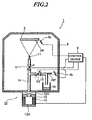
- Fig. 2 is an explanatory view showing a film formation source and a film formation apparatus containing the film formation source, according to another embodiment of the present invention which is a more detailed example based on the above-described embodiment (elements which are the same as those described above will be represented by the same reference numerals and the related descriptions will be partially omitted).
- this embodiment is characterized by a film formation material collection device 16 provided at the end of the escape passage 15.
- the film formation material collection device 16 is provided at the end of the escape passage 15, so that it is possible to collect the film formation material passing through the escape passage 15.
- the film formationmaterial collection device 16 can collect the film formation material passing through the escape passage 15, it is allowed to omit an additional step for recovering the unused material, thereby making it possible to effectively reuse the film formation material and thus improving the economical efficiency of the film formation process.
- the present invention should not be limited by this. Actually, it is also possible to extend the escape passage 15 so that its front end is disposed on the outside of the film formation chamber 2 and the film formationmaterial collection device 16 is allowed to be connected with the escape passage 15 outside the film formation chamber 2. In this way, it is possible to reuse the film formation material collected by the film formation material collection device 16 without breaking the vacuum state of the film formation chamber 2. Also, since it is possible to exchange the film formation material collection device 16 (filled with the film formation material) without breaking the vacuum state of the film formation chamber 2, it is allowed to improve the efficiency of the film formation process, thereby ensuring a smooth and continuous film formation operation.
- the present embodiment ischaracterized by providing, on one or each of the discharge passage 14 and the escape passage 15, a detection port 15P for detecting the flowing state of the film formation material, and detectors 4a, 4b (detection device, thickness monitoring device or the like) for detecting the film formation material in the vicinity of the substrate 3 or discharged from the detection port 15P.
- the film formation apparatus 1 has a control unit 5 (control device) for controlling the valves V1, V2 in accordance with the detection results of the detectors 4a, 4b.
- the control unit 5 can control the heating device 13 of the material accommodating section 12.
- the control unit 5 can control both of the valves V1 and V2, as well as the heating device 13.
- the detector 4a to detect the film formation material discharged from the discharge passage 14 and by controlling the opening degrees of the valves V1, V2 in accordance with the detection results, it is possible to freely control the discharge state (for example, vapor deposition rate) from the discharge outlet 11, without decomposing the film formation material contained in the film formation source 10, nor causing an increased pressure higher than a predetermined range.
- the discharge state for example, vapor deposition rate
- the flow restricting valve V1 is closed to some extent, whereas the flow restricting valve V2 is opened, thereby inhibiting the high rate discharge state so as to obtain a uniform discharge rate, and controlling the inner pressure of the film formation source 10 within a desired pressure range which ensures an acceptable film formation.
- the detector 4b to detect the film formation material discharged from the detection port 15P (located on the downstream side of the flow restricting valve V2 of the escape passage 15), and by opening or closing the valves V1, V2 in accordance with the detection results, it is possible to perform a control to change one state (wherein the flow restricting valve V1 is closed and the flow restricting valve V2 is opened) to another (wherein the flow restricting valve V1 is opened and the flow restricting valve V2 is closed), in response to the discharge state (such as a standup state at the beginning of a heating process) from the material accommodating section 12.
- the control unit 5 will operate to open the flow restricting valve V2 and at the same time close the flow restricting valve V1.
- the heating device 13 is maintained at its operative state and if the valve V1 is opened and the valve V2 is closed, it is possible for the apparatus to quickly return back to its previous operation state existing before the stopping.
- the apparatus does not require any urgent restoration for returning back, it is allowed to close the valve V1 and open the valve V2, as well as to stop the operation of the heating device 13.
- Fig. 3 is an explanatory view showing a film formation source formed according to another embodiment of the present invention and a film formation apparatus containing the film formation source (elements which are the same as those in the foregoing embodiment will be represented by the same reference numerals and the description thereof will be partially omitted).
- the material accommodating section 12 has detachable or exchangeable material containers 12A 1 and 12A 2 which are connected with discharge passages 14 1 and 14 2 communicated with their common discharge outlet 11.
- the first material container 12A 1 of the material accommodating section 12 disposed outside the film formation chamber 2 is connected with the discharge passage 14 1 and communicated with the discharge outlet 11 through the discharge passage 14 1
- the second material container 12A 2 is connected with the discharge passage 14 2 and communicated with the discharge outlet 11 through the discharge passage 14 2 .
- escape passages 15 1 , 15 2 are branching from the discharge passages 14 1 , 14 2 and are connected through their end portions to film formation material collection device 16.
- escape passages 15 1 , 15 2 are communicated with each other at their end portions and connected to the film formation material collection device 16, it is also possible to provide one film formation material collection device 16 at the end of each of the escape passages 15 1 , 15 2 .
- the material containers 12A 1 and 12A 2 are used to hold different materials, it is necessary for each of the escape passages 15 1 , 15 2 to have its own film formation material collection device 16.
- the film formation material collection device 16 is installed within the film formation chamber 2, it is also possible to extend the escape passages 15 1 , 15 2 so that their end portions are disposed on the outside of the film formation chamber 2, thereby allowing the film formation material collection device 16 to be installed outside the film formation chamber 2.
- the flow restricting valves V1 and V2 are provided on the discharge passage 14 1 of the first material container 12A 1 and on the escape passage 15 1
- the flow restricting valves V3 and V4 are provided on the discharge passage 14 2 of the second material container 12A 2 and on the escape passages 15 2 .
- the material accommodating section 12 contains heating devices 13 1 and 13 2 located within the first material container 12A 1 and the second material container 12A 2 . Further, a heat-insulator 16a is provided in the film formation material collection device 16, while a cooling unit 16b is formed beneath the heat-insulator 16a. Besides, although an example illustrated herein involves two material containers 12A 1 and 12A 2 , it is also possible to include three or more material containers which have similar structures.
- the film formation apparatus 1 containing the film formation source 10 By using the film formation source 10, the film formation apparatus 1 containing the film formation source 10, and the method employing the film formation apparatus 1, it is possible for each of the discharge passages 14 1 , 14 2 of the material containers 12A 1 , 12A 2 as well as the escape passages 15 1 , 15 2 to obtain the same effect as obtained in the foregoing embodiment. As compared with the foregoing embodiment, the present embodiment is suitable for carrying out continuous film formation during a prolonged time.
- film formation material within the first material container 12A 1 is heated by the heading device 13 1 so as to be discharged from the first material container 12A 1 .
- the flow restricting valve V1 is closed and the flow restricting valve V2 is opened, so that it is allowed to perform a pre-heating until the discharge from the first material container 12A 1 reaches a desired state.
- the flow restricting valve V1 is opened and the flow restricting valve V2 is closed, so as to discharge the film formationmaterial from the first material container 12A 1 through the discharge outlet 11, thereby effecting the film formation on the film formation surface 3A of the substrate 3.
- pre-heating is started to heat the film formation material within the second material container 12A 2 . Namely, prior to shutting the discharge passage 14 1 of the first material container 12A 1 , heating is started to heat the film formation material in the second material container 12A 2 until the discharge from the second material container 12A 2 reaches a predetermined state.
- the flow restricting valve V3 is closed to shut the discharge passage 14 2 of the second material container 12A 2 , while the flow restricting valve V4 is opened to open the escape-passage 15 2 . Then, after the discharge from the second material container 12A 2 has reached a predetermined state, the flow restricting valve V3 is opened to open the discharge passage 14 2 , while the flow-restricting valve V4 is closed to shut the escape-passage 15 2 .
- the discharge changeover is performed during a period in which the discharge outlet 11 does not directly face the film formation surface 3A of the substrate 3.
- the discharge changeover is preferred to be performed after a treated substrate has been moved away and before an untreated substrate is moved into the film formation chamber 2.
- the discharge changeover is carried out with a shielding plate (such as shutter) interposed between the film formation surface 3A and the discharge outlet 11.
- the flow restricting valves V1-V4 can be controlled at the states shown in the following Table 1.
- the material discharge from the discharge outlet 11 is controlled within a minimum time period required only for the opening or closing of the valves, thereby ensuring a smooth changeover from the discharge out of the first material container 12A 1 to the discharge out of the second material container 12A 2 . Further, even when the discharge out of the first material container 12A 1 has been changed over to the discharge out of the second material container 12A 2 , there would be no deviation in the position of the discharge outlet 11 since the discharge outlet 11 is common to discharges from both the first material container 12A 1 and the second material container 12A 2 , thus allowing the substrate 3 and the detector 4a to be fixed in their original positions.
- the discharge passage 14 1 of the first material container 12A 1 is to be closed, since at this time the discharge from the first material container 12A 1 does not stop immediately even if the heating of the first material container 12A 1 is stopped, the discharge passage 14 1 shall be closed and the escape-passage 15 1 shall be opened, thereby allowing the film formation material collection device 16 to collect the remaining film formation material. Then, after the discharge from the first material container 12A 1 has been accumulated to some extent, the gate-valve 12V in connection with the first material container 12A 1 is closed, so that the first material container 12A may be removed to supplement the film formation material therein or replaced by a new material container. Subsequently, since it is allowed to perform similar changeover from the second material container 12A 2 to the first material container 12A 1 , a repeated operation makes it possible to perform continuous film formation under the same condition for a long time.
- the present embodiment is further improved by controlling the discharge state in accordance with the detection result of the detector 4a described in the embodiment of Fig. 2 , it is possible to perform a high precision film formation for a long time period.
- valve changeover is controlled in accordance with the detection result of the detector 4b, it is possible to realize a continuous film formation for a long time by performing an automatic changeover.
- the film formation material contained in the first material container 12A 1 is the same as the film formation material contained in the second material container 12A 2 , so that it is possible to perform a continuous film formation for a long time period, as described above.
- the film formation material contained in the first material container 12A 1 is different from the film formation material contained in the second material container 12A 2 , it is possible to effect a smooth changeover from one film formation based on one film formation material to another film formation based on another film formation material, by virtue of the same effect as described above.
- each of the flow restricting valves V1-V4 mentioned above can be formed by an independently variable adjusting valve. However, if it is difficult to ensure an adequate durability as well as an adequate reliability during full closure of valve, it is allowed to form a combination of ON-OFF valves (capable of effecting a changeover between closing and opening) with variable adjusting valves. Moreover, although not shown in the accompanying drawings, it is also possible to employ a three-way valve or a combination of the three-way valve with valves V1 and V2. Besides, as to the flow restricting valves V2, V4 provided on the escape passages 15,15 1 ,15 2 , it is allowed to use only ON-OFF valves capable of effecting a changeover between closing and opening (but not having variable adjusting function). In addition, the flow restricting valves V1-V4 are not absolutely necessary to be valves, but can be replaced by other flow restricting device such as shutters.
- heating device in one of other positions not included in the material accommodating section 12, such as the discharge passages 14, 14 1 , 14 2 , the escape passages 15,15 1 ,15 2 , the discharge outlet 11, and the detection ports 14P, 15P. In this way, it is possible to ensure smoother flowing or discharge of the film formation material from the material accommodating section 12.
- the film formation apparatus 1 mentioned above may be a vacuum deposition apparatus using a resistance heating method, a high-frequency heating method, a laser heating method, or an electron beam heating method.
- a method for use in the vacuum deposition apparatus 1 should not be limited as such.
- the film formation chamber 2 may be a vacuum chamber set at a high vacuum condition (10 -4 Pa or less), while the material accommodating section 12 may be a container formed by a high-melting point oxide such as alumina (Al 2 O 3 ) and Beryllia (BeO), and surrounded by a heating device 13 consisting of high melting point filament such as tantalum (Ta), molybdenum (Mo), and tungsten (W), or consisting of a boat-like heating coil.
- the film formation may be a discontinuous process in which substrates are treated individually or an inline type process inwhich substrates are treated continuously.
- the discharge outlet 11 is arranged to face upward and the film formation surface 3A is arranged to face downward
- the present invention shouldnot be limitedby such a specific example.
- the discharge outlet 11 it is also possible for the discharge outlet 11 to face in the horizontal direction and the substrate 3 in an upright direction so that its film formation surface 3A can face the discharge outlet 11.
- the discharge outlet can have any desired shape which may be circular or rectangular, and it is also possible to employ a plurality of such discharge outlets in order to continuously effect a uniform film formation on the film formation surface 3A.
- the above-described film formation apparatus 1 and the film formation method using the film formation apparatus 1 are suitable for manufacturing an organic EL panel.
- Such an organic EL panel includes a substrate and organic EL devices formed on the substrate, each organic EL device has a pair of electrodes including a first electrode and a second electrode, an organic layer interposed between the pair of electrodes, such an organic layer contains an organic luminescent layer.
- at least one sort of film formation material for forming the electrodes or the organic material layer is formed into a filmon the substrate 3, it is allowed to use the above-described film formation apparatus 1 and the film formation method using the film formation apparatus 1.
- Fig. 4 is an explanatory view showing an example of an organic EL panel manufactured by the above-described manufacturing method.
- the organic EL panel 100 is formed by interposing an organic layer 33 containing an organic luminescent layer between first electrodes 31 on one hand and second electrodes 32 on the other, thereby forming a plurality of organic EL devices 30 on the substrate 20.
- a silicone coating layer 20a is formed on the substrate 20, and a plurality of first electrodes 31 consisting of transparent electrode material such as ITO and serving as cathodes are formed on the silicon coating layer 20a.
- second electrodes 32 consisting of a metal and serving as anodes are formed above the first electrodes 31, thereby forming a bottom emission type panel producing light from the substrate 20 side.
- the panel also contains an organic layer 33 including a hole transporting layer 33A, a luminescent layer 33B, and an electron transporting layer 33C. Then, a cover 40 is bonded to the substrate 20 through an adhesive layer 41, thereby forming a sealing space M on the substrate 20 and thus forming a display section consisting of organic EL devices 30 within the sealing space M.
- an organic layer 33 including a hole transporting layer 33A, a luminescent layer 33B, and an electron transporting layer 33C.
- the organic EL devices 30 are formed such that the first electrodes 31 are separated by a plurality of insulating strips 34, thereby forming luminescent units (30R, 30G, 30B) under the first electrodes 31. Moreover, a desiccant layer 42 is attached to the inner surface of the cover 40, thereby preventing the organic EL devices 30 from getting deteriorated due to moisture.
- first electrode layer 21A using the same material and the same step as forming the first electrodes 31, which is separated from the first electrodes 31 by the insulating strips 34.
- second electrode layer 21B containing a silver-palladium (Ag-Pd) alloy and forming a low-resistant wiring portion.
- a protection coating layer 21C consisting of IZO or the like is formed on the second electrode layer 21C. In this way, a lead-out electrode 21 can be formed which consists of the first electrode layer 21A, the second electrode layer 21B, and the protection coating 21C. Then, an end portion 32a of each second electrode 32 is connected to the lead-out electrode 21 within the sealing space M.
- each first electrode 31 is not shown in the drawing, it is possible to elongate each first electrode 31 and lead the same out of the sealing space M.
- lead-out electrode can also be formed into an electrode layer containing Ag-Pd alloy or the like and constituting a low resistant wiring portion.
- Either the first electrodes 31 or the second electrodes 32 are set as cathode side, while the opposite side is set as anode side.
- the anode side is formed by a material having a higher work function than the cathode side, using a transparent conductive film which may be a metal film such as chromium (Cr), molybdenum (Mo), nickel (Ni), and platinum (Pt), or a metal oxide film such as ITO and IZO.
- the cathode side is formed by a material having a lower work function than the anode side, using a metal having a low work function, which may be an alkali metal (such as Li, Na, K, Rb, and Cs), an alkaline earth metal (such as Be, Mg, Ca, Sr, and Ba), a rare earth metal, a compound or an alloy containing two or more of the above elements, or an amorphous semiconductor such as a doped polyaniline and a doped polyphenylene vinylene, or an oxide such as Cr 2 O 3 , NiO, and Mn 2 O 5 .
- a metal having a low work function which may be an alkali metal (such as Li, Na, K, Rb, and Cs), an alkaline earth metal (such as Be, Mg, Ca, Sr, and Ba), a rare earth metal, a compound or an alloy containing two or more of the above elements, or an amorphous semiconductor such as a doped polyaniline and a do
- the lead-out electrodes (the lead-out electrode 14 and the lead-out electrode of the first electrodes 31) are connected with drive circuit parts driving the organic EL panel 100 or connected with a flexible wiring board.
- these lead-out electrodes it is preferable for these lead-out electrodes to be formed as having a low resistance.
- the lead-out electrodes can be formed by laminating low resistant metal electrode layers which may be Ag-Pd alloy or APC, Cr, A1, or may be formed by single one electrode of low resistant metal.
- the organic layer 33 comprises one or more layers of organic compound materials including at least one organic luminescent layer
- its laminated structure can be in any desired arrangement.
- a laminated structure including, from the anode side towards the cathode side, a hole transporting layer 33A, a luminescent layer 33B, and an electron transporting layer 33C.
- Each of the hole transporting layer 33A, the luminescent layer 33B, and the electron transporting layer 33C can be in a single-layer or a multi-layered structure.
- the hole transporting layer 33A, the luminescent layer 33B, and the electron transporting layer 33C can be formed by any conventional materials (it is allowed to use either a high molecular material or a low molecular material).
- a luminescent material for forming the luminescent layer 4B it is allowed to make use of a luminescence (fluorescence) when the material returns from a singlet excited state to a base state or a luminescence (phosphorescence) when it returns from a triplet excited state to a base state.
- a luminescence fluorescence
- phosphorescence luminescence
- the organic EL panel 100 is a panel formed by tightly covering organic EL devices 30 with a covering member 40 made of metal, glass, or plastic.
- the covering member may be a piece of material having a recess portion (a one-step recess or a two-step recess) formed by pressing, etching, or blasting.
- the covering member may be formed by using a flat glass plate and includes an internal covering space M to be formed between the flat glass plate and the substrate by virtue of a spacer made of glass (or plastic).
- an inorganic material may be a nitride such as SiN, AlN, and GaN, or an oxide such as SiO, Al 2 O 3 , Ta 2 O 5 , ZnO, and GeO, or an oxidized nitride such as SiON, or a carbonized nitride such as SiCN, or a metal fluorine compound, or a metal film, etc.
- an organic material may be an epoxy resin, or an acryl resin, or a paraxylene resin, or a fluorine systemhighmolecule such as perfluoro olefin andperfluoro ether, or a metal alkoxide such as CH 3 OM and C 2 H 5 OM, or a polyimide precursor, or a perylene system compound, etc.
- a fluorine systemhighmolecule such as perfluoro olefin andperfluoro ether
- a metal alkoxide such as CH 3 OM and C 2 H 5 OM
- polyimide precursor such as a perylene system compound, etc.
- An adhesive agent forming the adhesive layer 41 may be a thermal-setting type, a chemical-setting type (2-liquid mixture), or a light (ultraviolet) setting type, which can be formed by an acryl resin, an epoxy resin, a polyester, a polyolefine. Particularly, it is preferable to use an ultraviolet-setting epoxy resin adhesive agent which is quick to solidify without a heating treatment.
- Desiccating material 42 may be a physical desiccating agent such as zeolite, silica gel, carbon, and carbon nanotube; a chemical desiccating agent such as alkali metal oxide, metal halogenide, peroxide chlorine; a desiccating-agent formed by dissolving an organic metallic complex in a petroleum system solvent such as toluene, xylene, an aliphatic organic solvent and the like; and a desiccating agent formed by dispersing desiccating particles in a transparent binder such as polyethylene, polyisoprene, polyvinyl thinnate.
- a physical desiccating agent such as zeolite, silica gel, carbon, and carbon nanotube
- a chemical desiccating agent such as alkali metal oxide, metal halogenide, peroxide chlorine
- a desiccating-agent formed by dissolving an organic metallic complex in a petroleum system solvent such as toluene, xylene, an aliphatic organic
- the organic EL panel 100 of the present invention can have various types without departing from the scope of the invention.
- the light emission type of an organic EL device 30 can be a bottom emission type emitting light from the substrate 20 side, or a top emission type emitting light from a side opposite to the substrate 20.
- the EL display panel may be a single color display or a multi-color display.
- CF method, CCM method color conversion layer formed by a color filter or a fluorescent material
- SOLED transparent Stacked OLED
- the present invention at the time of supplementing film formation material to the film formation source 10 or exchanging the film formation source, since it is not necessary to break a vacuum condition or a reduced pressure condition within the film formation chamber 2, it is allowed to shorten an operation time for performing the film formation, thereby ensuring an increased efficiency for the film formation operation. Further, even if the material containers 12A, 12A 1 and 12A 2 of the film formation source 10 are changed over to different materials, film formations using different materials can still be carried out within the same film formation chamber 2.
- the organic EL panel manufacturing process including a film formation step using various materials, it is possible to improve the productivity and thus reduce production cost. Moreover, it is possible to improve the film formation precision and thus increase product yield. Further, since the use of the film formation material collection device 16 makes it possible to increase the recovery rate of the material discharged but not used in the film formation, it is sure to reduce the production cost.
Landscapes
- Chemical & Material Sciences (AREA)
- Chemical Kinetics & Catalysis (AREA)
- Engineering & Computer Science (AREA)
- Materials Engineering (AREA)
- Mechanical Engineering (AREA)
- Metallurgy (AREA)
- Organic Chemistry (AREA)
- Electroluminescent Light Sources (AREA)
- Physical Vapour Deposition (AREA)
Claims (12)
- Dispositif de formation de film (1) ayant une chambre de formation de film (2) dans laquelle un état de vide ou un état sans pression est formé et une matière de formation de film sublimée ou évaporée est formée dans un film sur un substrat (3),ledit dispositif comportant une source de formation de film qui comporte en outre :une sortie d'évacuation (11) disposée à l'intérieur de la chambre de formation de film (2) pour évacuer la matière de formation de film en direction d'une surface de formation de film (3A) du substrat (3),une partie réceptrice de matière (12) disposée à l'extérieur de la chambre de formation de film (2) et incluant un conteneur de matière (12A) contenant la matière de formation de film,un dispositif de chauffage (13) pour chauffer la matière de formation de film contenue dans le conteneur de matière (12A),un passage d'évacuation (14) disposé à l'intérieur de la chambre de formation de film (2) et faisant communiquer de manière étanche à l'air la sortie d'évacuation (11) et la partie réceptrice de matière (12),un passage d'échappement (15) disposé à l'intérieur de la chambre de formation de film (2) et bifurquant à partir du passage d'évacuation (14) pour dévier la matière de formation de film se déplaçant vers la sortie de décharge (11) dans une direction différente, etdes dispositifs de restriction d'écoulement (V1, V2) agencés au moins sur le côté aval d'une position de bifurcation du passage d'évacuation (14) et sur le passage d'échappement (15), pour arrêter/laisser passer ou régler de manière variable l'écoulement de la matière de formation de film,dans lequel, sur le passage d'évacuation et/ou le passage d'échappement sont agencés un orifice de détection (14P, 15P) pour détecter un état d'écoulement de la matière de formation de film, ainsi qu'un dispositif de détection (4a, 4b) disposé à l'intérieur de la chambre de formation de film (2) pour détecter la matière de formation de film évacuée à partir de l'orifice de détection.
- Dispositif de formation de film selon la revendication 1, dans lequel un dispositif de collecte de matière de formation de film (16) est disposé à une extrémité du passage d'échappement (15).
- Dispositif de formation de film selon la revendication 2, dans lequel le dispositif de collecte de matière de formation de film (16) est disposé à l'extérieur de la chambre de formation de film (2).
- Dispositif de formation de film selon l'une quelconque des revendications 1 à 3, dans lequel la partie réceptrice de matière (12) inclut une pluralité de conteneurs de matière amovibles ou échangeables (12A, 12A1, 12A2), alors qu'une pluralité de passages d'évacuation (14, 141,142) est agencée en liaison avec les conteneurs de matière (12A, 12A1, 12A2) et en communication avec une sortie d'évacuation commune (11).
- Dispositif de formation de film selon la revendication 1, 2 ou 3, comportant également un dispositif de commande (5) pour commander les dispositifs de restriction d'écoulement (V1, V2), lequel dispositif de commande fonctionne pour commander les dispositifs de restriction d'écoulement en fonction d'un résultat de détection du dispositif de détection (4b).
- Procédé de formation de film dans lequel une sortie d'évacuation (11) est amenée en vis-à-vis d'une surface de formation de film (3A) d'un substrat (3) disposé à l'intérieur d'une chambre de formation de film (2) maintenue à un état de vide ou sans pression, une matière de formation de film sublimée ou évaporée par chauffage dans une partie réceptrice de matière (12) disposée à l'extérieur de la chambre de formation de film (2) peut s'écouler à travers un passage d'évacuation et être évacuée par la sortie d'évacuation (11) de manière à former un film sur la surface de formation de film (3A),dans lequel un passage d'échappement (15) est créé par une bifurcation à partir du passage d'évacuation (14) pour dévier la matière de formation de film se déplaçant vers la sortie d'évacuation (11) dans une direction différente,dans lequel un écoulement à travers le passage d'échappement (15) est débuté lorsque l'écoulement de la matière de formation de film est arrêté ou restreint sur le côté aval d'une position de bifurcation du passage d'évacuation (14),dans lequel, sur le passage d'évacuation et/ou le passage d'échappement, sont agencés un orifice de détection (14P, 15P) pour détecter un état d'écoulement de la matière de formation de film, ainsi qu'un dispositif de détection (4a, 4b) disposé à l'intérieur de la chambre de formation de film (2) pour détecter la matière de formation de film évacuée depuis l'orifice de détection,un dispositif de commande (5) pour commander les dispositifs de restriction d'écoulement (V1, V2), lequel dispositif de commande fonctionne pour commander les dispositifs de restriction d'écoulement en fonction d'un résultat de détection du dispositif de détection (4a, 4b).
- Procédé de formation de film selon la revendication 6, dans lequel le passage d'évacuation (14) est maintenu fermé et le passage d'échappement (15) est maintenu ouvert jusqu'à ce qu'un état d'évacuation depuis la partie réceptrice de matière (12) atteigne un état prédéterminé,dans lequel, après que l'état d'évacuation depuis la partie réceptrice de matière (12) ait atteint un état prédéterminé, le passage d'évacuation est ouvert et le passage d'échappement (15) est fermé.
- Procédé de formation de film selon la revendication 7, dans lequel la partie réceptrice de matière (12) inclut une pluralité de conteneurs de matière amovibles ou échangeables (12A, 12A1, 12A2), alors qu'une pluralité de passages d'évacuation (14, 141,142) est agencée en liaison avec les conteneurs de matière et en communication avec une sortie d'évacuation commune (11),dans lequel, avant de fermer un passage d'évacuation mis en communication avec un premier conteneur de matière de la partie réceptrice de matière (12), un chauffage est démarré pour chauffer un second conteneur de matière de la partie réceptrice de matière (12),dans lequel un passage d'évacuation mis en communication avec un second conteneur de matière est maintenu fermé et un passage d'échappement bifurquant à partir du passage d'évacuation est maintenu ouvert jusqu'à ce qu'un état d'évacuation depuis le second conteneur de matière atteigne un état prédéterminé,dans lequel, après que l'état d'évacuation depuis le second conteneur de matière ait atteint un état prédéterminé, le passage d'évacuation mis en communication avec le second conteneur de matière est ouvert et le passage d'échappement bifurquant à partir du passage d'évacuation est fermé.
- Procédé de formation de film selon la revendication 8, dans lequel, après que le passage d'évacuation mis en communication avec le second conteneur de matière ait été ouvert, le passage d'échappement bifurquant à partir du passage d'évacuation mis en communication avec le premier conteneur de matière est également ouvert, et le passage d'évacuation mis en communication avec le premier conteneur de matière est fermé.
- Procédé de formation de film selon l'une quelconque des revendications 6 à 9, dans lequel la sortie d'évacuation (11) et la surface de formation de film (3A) du substrat (3) ne sont pas amenées l'une en face de l'autre, et l'évacuation à travers le passage d'échappement mis en communication avec le premier conteneur de matière est basculée sur l'évacuation à travers le passage d'évacuation mis en communication avec le second conteneur de matière.
- Procédé de formation de film selon l'une quelconque des revendications 6 à 10, dans lequel un dispositif de collecte de matière de formation de film (16) est disposé à l'extrémité des passages d'échappement (15, 151,152) pour collecter la matière de formation de film passant à travers les passages d'échappement (15, 151,152).
- Procédé de fabrication d'un panneau EL organique (100) comportant un substrat (20) et au moins un dispositif EL organique (30) formé sur le substrat (20), ledit au moins un dispositif EL organique (30) incluant une première électrode (31), une seconde électrode (32) et une couche de matière organique (33) intercalée entre les première et seconde électrodes, ladite couche de matière organique (33) contenant une couche luminescente organique,dans lequel au moins un type de matière de formation de film pour former la première électrode (31), la seconde électrode (32) ou la couche de matière organique (33) est formé dans un film sur le substrat (20), en utilisant un dispositif de formation de film selon l'une quelconque des revendications 1 à 5 ou un procédé de formation de film selon l'une quelconque des revendications 6 à 10.
Applications Claiming Priority (2)
| Application Number | Priority Date | Filing Date | Title |
|---|---|---|---|
| JP2004099944 | 2004-03-30 | ||
| JP2004099944A JP4366226B2 (ja) | 2004-03-30 | 2004-03-30 | 有機elパネルの製造方法、有機elパネルの成膜装置 |
Publications (2)
| Publication Number | Publication Date |
|---|---|
| EP1584705A1 EP1584705A1 (fr) | 2005-10-12 |
| EP1584705B1 true EP1584705B1 (fr) | 2008-06-25 |
Family
ID=34909438
Family Applications (1)
| Application Number | Title | Priority Date | Filing Date |
|---|---|---|---|
| EP05004709A Expired - Fee Related EP1584705B1 (fr) | 2004-03-30 | 2005-03-03 | Source de vapeur pour dispositif de revêtement. |
Country Status (7)
| Country | Link |
|---|---|
| US (2) | US20050217584A1 (fr) |
| EP (1) | EP1584705B1 (fr) |
| JP (1) | JP4366226B2 (fr) |
| KR (1) | KR20060043241A (fr) |
| CN (1) | CN100446300C (fr) |
| DE (1) | DE602005007648D1 (fr) |
| TW (1) | TW200532046A (fr) |
Families Citing this family (59)
| Publication number | Priority date | Publication date | Assignee | Title |
|---|---|---|---|---|
| US7465475B2 (en) * | 2004-11-09 | 2008-12-16 | Eastman Kodak Company | Method for controlling the deposition of vaporized organic material |
| JP4583200B2 (ja) * | 2005-02-17 | 2010-11-17 | 日立造船株式会社 | 蒸着装置 |
| JP4545028B2 (ja) * | 2005-03-30 | 2010-09-15 | 日立造船株式会社 | 蒸着装置 |
| JP4402016B2 (ja) | 2005-06-20 | 2010-01-20 | キヤノン株式会社 | 蒸着装置及び蒸着方法 |
| JP2007227086A (ja) * | 2006-02-22 | 2007-09-06 | Tokyo Electron Ltd | 成膜装置および発光素子の製造方法 |
| JP2007232802A (ja) * | 2006-02-27 | 2007-09-13 | Hitachi Displays Ltd | 有機el表示装置 |
| JP5179739B2 (ja) | 2006-09-27 | 2013-04-10 | 東京エレクトロン株式会社 | 蒸着装置、蒸着装置の制御装置、蒸着装置の制御方法および蒸着装置の使用方法 |
| JP5127372B2 (ja) | 2007-09-03 | 2013-01-23 | キヤノン株式会社 | 蒸着装置 |
| JP5506147B2 (ja) * | 2007-10-18 | 2014-05-28 | キヤノン株式会社 | 成膜装置及び成膜方法 |
| EP2128303B1 (fr) * | 2008-05-30 | 2013-03-13 | Applied Materials, Inc. | Agencement pour le revêtement d'un substrat |
| WO2009144072A1 (fr) * | 2008-05-30 | 2009-12-03 | Applied Materials, Inc. | Dispositif de revêtement de substrat |
| JP2010159448A (ja) * | 2009-01-07 | 2010-07-22 | Canon Inc | 成膜装置及び成膜方法 |
| JP5328726B2 (ja) * | 2009-08-25 | 2013-10-30 | 三星ディスプレイ株式會社 | 薄膜蒸着装置及びこれを利用した有機発光ディスプレイ装置の製造方法 |
| JP5677785B2 (ja) | 2009-08-27 | 2015-02-25 | 三星ディスプレイ株式會社Samsung Display Co.,Ltd. | 薄膜蒸着装置及びこれを利用した有機発光表示装置の製造方法 |
| JP5410235B2 (ja) * | 2009-10-15 | 2014-02-05 | 小島プレス工業株式会社 | 有機高分子薄膜の形成方法及び形成装置 |
| US8876975B2 (en) | 2009-10-19 | 2014-11-04 | Samsung Display Co., Ltd. | Thin film deposition apparatus |
| JP5452178B2 (ja) * | 2009-11-12 | 2014-03-26 | 株式会社日立ハイテクノロジーズ | 真空蒸着装置、真空蒸着方法、および、有機el表示装置の製造方法 |
| JP5650234B2 (ja) * | 2009-11-16 | 2015-01-07 | エフ・イ−・アイ・カンパニー | ビーム処理システムに対するガス送達 |
| KR101146982B1 (ko) | 2009-11-20 | 2012-05-22 | 삼성모바일디스플레이주식회사 | 박막 증착 장치 및 유기 발광 디스플레이 장치 제조 방법 |
| KR101084234B1 (ko) * | 2009-11-30 | 2011-11-16 | 삼성모바일디스플레이주식회사 | 증착원, 이를 구비하는 증착 장치 및 박막 형성 방법 |
| KR101174874B1 (ko) * | 2010-01-06 | 2012-08-17 | 삼성디스플레이 주식회사 | 증착 소스, 박막 증착 장치 및 유기 발광 표시 장치 제조 방법 |
| KR101084184B1 (ko) | 2010-01-11 | 2011-11-17 | 삼성모바일디스플레이주식회사 | 박막 증착 장치 |
| KR101174875B1 (ko) | 2010-01-14 | 2012-08-17 | 삼성디스플레이 주식회사 | 박막 증착 장치, 이를 이용한 유기 발광 디스플레이 장치의 제조방법 및 이에 따라 제조된 유기 발광 디스플레이 장치 |
| KR101193186B1 (ko) | 2010-02-01 | 2012-10-19 | 삼성디스플레이 주식회사 | 박막 증착 장치, 이를 이용한 유기 발광 디스플레이 장치의 제조방법 및 이에 따라 제조된 유기 발광 디스플레이 장치 |
| KR101156441B1 (ko) * | 2010-03-11 | 2012-06-18 | 삼성모바일디스플레이주식회사 | 박막 증착 장치 |
| KR101202348B1 (ko) | 2010-04-06 | 2012-11-16 | 삼성디스플레이 주식회사 | 박막 증착 장치 및 이를 이용한 유기 발광 표시 장치의 제조 방법 |
| US8894458B2 (en) | 2010-04-28 | 2014-11-25 | Samsung Display Co., Ltd. | Thin film deposition apparatus, method of manufacturing organic light-emitting display device by using the apparatus, and organic light-emitting display device manufactured by using the method |
| KR101019947B1 (ko) * | 2010-06-10 | 2011-03-09 | 에스엔유 프리시젼 주식회사 | 유기 반도체 제조장치 |
| KR101223723B1 (ko) | 2010-07-07 | 2013-01-18 | 삼성디스플레이 주식회사 | 박막 증착 장치, 이를 이용한 유기 발광 디스플레이 장치의 제조방법 및 이에 따라 제조된 유기 발광 디스플레이 장치 |
| WO2012039383A1 (fr) * | 2010-09-22 | 2012-03-29 | 株式会社アルバック | Appareil de traitement sous vide et procédé de formation d'un film mince organique |
| JP5661416B2 (ja) * | 2010-10-15 | 2015-01-28 | キヤノン株式会社 | 蒸着装置 |
| KR101723506B1 (ko) | 2010-10-22 | 2017-04-19 | 삼성디스플레이 주식회사 | 유기층 증착 장치 및 이를 이용한 유기 발광 디스플레이 장치의 제조 방법 |
| KR101738531B1 (ko) | 2010-10-22 | 2017-05-23 | 삼성디스플레이 주식회사 | 유기 발광 디스플레이 장치의 제조 방법 및 이에 따라 제조된 유기 발광 디스플레이 장치 |
| KR20120045865A (ko) | 2010-11-01 | 2012-05-09 | 삼성모바일디스플레이주식회사 | 유기층 증착 장치 |
| KR20120065789A (ko) | 2010-12-13 | 2012-06-21 | 삼성모바일디스플레이주식회사 | 유기층 증착 장치 |
| KR101760897B1 (ko) | 2011-01-12 | 2017-07-25 | 삼성디스플레이 주식회사 | 증착원 및 이를 구비하는 유기막 증착 장치 |
| JP2012156073A (ja) * | 2011-01-28 | 2012-08-16 | Konica Minolta Holdings Inc | 真空蒸着装置、有機エレクトロルミネッセンス素子の製造方法及び有機エレクトロルミネッセンス素子 |
| KR101852517B1 (ko) | 2011-05-25 | 2018-04-27 | 삼성디스플레이 주식회사 | 유기층 증착 장치 및 이를 이용한 유기 발광 디스플레이 장치의 제조 방법 |
| KR101840654B1 (ko) | 2011-05-25 | 2018-03-22 | 삼성디스플레이 주식회사 | 유기층 증착 장치 및 이를 이용한 유기 발광 디스플레이 장치의 제조 방법 |
| KR101857249B1 (ko) | 2011-05-27 | 2018-05-14 | 삼성디스플레이 주식회사 | 패터닝 슬릿 시트 어셈블리, 유기막 증착 장치, 유기 발광 표시장치제조 방법 및 유기 발광 표시 장치 |
| KR101826068B1 (ko) | 2011-07-04 | 2018-02-07 | 삼성디스플레이 주식회사 | 유기층 증착 장치 |
| KR20130015144A (ko) | 2011-08-02 | 2013-02-13 | 삼성디스플레이 주식회사 | 증착원어셈블리, 유기층증착장치 및 이를 이용한 유기발광표시장치의 제조 방법 |
| JP5511767B2 (ja) * | 2011-10-27 | 2014-06-04 | 東京エレクトロン株式会社 | 蒸着装置 |
| JP2012088731A (ja) * | 2011-12-07 | 2012-05-10 | Hitachi Displays Ltd | 有機el表示装置 |
| JP2013163845A (ja) * | 2012-02-10 | 2013-08-22 | Nitto Denko Corp | 蒸着用坩堝及び蒸着装置並びに蒸着方法 |
| JP6021377B2 (ja) * | 2012-03-28 | 2016-11-09 | 日立造船株式会社 | 真空蒸着装置および真空蒸着装置におけるるつぼ交換方法 |
| JP5840055B2 (ja) * | 2012-03-29 | 2016-01-06 | 日立造船株式会社 | 蒸着装置 |
| JP2013209702A (ja) * | 2012-03-30 | 2013-10-10 | Nitto Denko Corp | 蒸着装置及び蒸着方法 |
| JP5460773B2 (ja) * | 2012-04-23 | 2014-04-02 | キヤノン株式会社 | 成膜装置及び成膜方法 |
| JP6013071B2 (ja) * | 2012-08-06 | 2016-10-25 | 株式会社カネカ | 真空蒸着装置 |
| KR101994838B1 (ko) | 2012-09-24 | 2019-10-01 | 삼성디스플레이 주식회사 | 유기층 증착 장치, 이를 이용한 유기 발광 디스플레이 장치의 제조 방법 및 이에 따라 제조된 유기 발광 디스플레이 장치 |
| EP2746423B1 (fr) * | 2012-12-20 | 2019-12-18 | Applied Materials, Inc. | Système de dépôt, appareil de dépôt et procédé de fonctionnement |
| CN104099570B (zh) * | 2013-04-01 | 2016-10-05 | 上海和辉光电有限公司 | 单点线性蒸发源系统 |
| KR102111020B1 (ko) * | 2013-05-02 | 2020-05-15 | 삼성디스플레이 주식회사 | 증착 장치 |
| JP6302786B2 (ja) * | 2014-08-01 | 2018-03-28 | シャープ株式会社 | 蒸着装置、蒸着方法、及び有機el素子の製造方法 |
| DE102014014970B4 (de) * | 2014-10-14 | 2020-01-02 | NICE Solar Energy GmbH | Vorrichtung und Verfahren zur Schichtdickenmessung für Dampfabscheideverfahren |
| CN108520833B (zh) * | 2018-03-16 | 2019-09-17 | 江苏中天科技股份有限公司 | 多孔铝宏观体及其制造系统与方法 |
| CN108265267B (zh) * | 2018-03-26 | 2020-01-21 | 京东方科技集团股份有限公司 | 一种线性蒸发源及蒸镀装置 |
| JP7200083B2 (ja) | 2019-10-31 | 2023-01-06 | 日立造船株式会社 | 真空蒸着装置の制御方法 |
Family Cites Families (30)
| Publication number | Priority date | Publication date | Assignee | Title |
|---|---|---|---|---|
| US3690933A (en) * | 1970-05-21 | 1972-09-12 | Republic Steel Corp | Apparatus and method for continuously condensing metal vapor upon a substrate |
| US4325986A (en) * | 1979-05-29 | 1982-04-20 | University Of Delaware | Method for continuous deposition by vacuum evaporation |
| JP2774351B2 (ja) * | 1990-03-26 | 1998-07-09 | 出光興産株式会社 | 有機薄膜エレクトロルミネッセンス素子及びその製造方法 |
| JPH04323362A (ja) * | 1991-04-19 | 1992-11-12 | Ulvac Japan Ltd | 多層膜の形成方法およびその形成装置 |
| JP2000252269A (ja) * | 1992-09-21 | 2000-09-14 | Mitsubishi Electric Corp | 液体気化装置及び液体気化方法 |
| JPH06295862A (ja) * | 1992-11-20 | 1994-10-21 | Mitsubishi Electric Corp | 化合物半導体製造装置及び有機金属材料容器 |
| JPH06196419A (ja) * | 1992-12-24 | 1994-07-15 | Canon Inc | 化学気相堆積装置及びそれによる半導体装置の製造方法 |
| JPH0784650A (ja) * | 1993-07-23 | 1995-03-31 | Hitachi Metals Ltd | マスフローコントローラ、その運転方法及び電磁弁 |
| JP3328389B2 (ja) * | 1993-09-14 | 2002-09-24 | 康夫 垂井 | 強誘電体薄膜の製造方法 |
| US5776254A (en) * | 1994-12-28 | 1998-07-07 | Mitsubishi Denki Kabushiki Kaisha | Apparatus for forming thin film by chemical vapor deposition |
| US5648175A (en) * | 1996-02-14 | 1997-07-15 | Applied Materials, Inc. | Chemical vapor deposition reactor system and integrated circuit |
| US5871813A (en) * | 1997-03-05 | 1999-02-16 | Applied Materials, Inc. | Apparatus and method for controlling process chamber pressure |
| US5968588A (en) * | 1997-03-17 | 1999-10-19 | Applied Materials, Inc. | In-situ liquid flow rate estimation and verification by sonic flow method |
| US5925980A (en) * | 1997-05-01 | 1999-07-20 | Motorola, Inc. | Organic electroluminescent device with graded region |
| US6258170B1 (en) * | 1997-09-11 | 2001-07-10 | Applied Materials, Inc. | Vaporization and deposition apparatus |
| US6037241A (en) * | 1998-02-19 | 2000-03-14 | First Solar, Llc | Apparatus and method for depositing a semiconductor material |
| US6197119B1 (en) * | 1999-02-18 | 2001-03-06 | Mks Instruments, Inc. | Method and apparatus for controlling polymerized teos build-up in vacuum pump lines |
| US20020011205A1 (en) * | 2000-05-02 | 2002-01-31 | Shunpei Yamazaki | Film-forming apparatus, method of cleaning the same, and method of manufacturing a light-emitting device |
| US7517551B2 (en) * | 2000-05-12 | 2009-04-14 | Semiconductor Energy Laboratory Co., Ltd. | Method of manufacturing a light-emitting device |
| EP1354979A4 (fr) * | 2000-08-10 | 2008-03-26 | Nippon Steel Chemical Co | Procede et dispositif pour produire des elements el organiques |
| US6558735B2 (en) * | 2001-04-20 | 2003-05-06 | Eastman Kodak Company | Reusable mass-sensor in manufacture of organic light-emitting devices |
| US6896929B2 (en) * | 2001-08-03 | 2005-05-24 | Applied Materials, Inc. | Susceptor shaft vacuum pumping |
| US6649436B2 (en) * | 2002-02-11 | 2003-11-18 | Eastman Kodak Company | Using organic materials in making an organic light-emitting device |
| JP2003257635A (ja) * | 2002-03-01 | 2003-09-12 | Ulvac Japan Ltd | 薄膜形成方法 |
| US20030168013A1 (en) * | 2002-03-08 | 2003-09-11 | Eastman Kodak Company | Elongated thermal physical vapor deposition source with plural apertures for making an organic light-emitting device |
| US6749906B2 (en) * | 2002-04-25 | 2004-06-15 | Eastman Kodak Company | Thermal physical vapor deposition apparatus with detachable vapor source(s) and method |
| JP2004014311A (ja) * | 2002-06-07 | 2004-01-15 | Sony Corp | 有機薄膜の形成方法 |
| JP2004043853A (ja) * | 2002-07-10 | 2004-02-12 | Sony Corp | 薄膜形成装置および薄膜形成方法 |
| WO2004105095A2 (fr) * | 2003-05-16 | 2004-12-02 | Svt Associates Inc. | Evaporateur a depot de film mince |
| JP2005082880A (ja) * | 2003-09-11 | 2005-03-31 | Shoka Kagi Kofun Yugenkoshi | 有機el発光装置の成膜設備 |
-
2004
- 2004-03-30 JP JP2004099944A patent/JP4366226B2/ja not_active Expired - Lifetime
-
2005
- 2005-02-28 KR KR1020050016494A patent/KR20060043241A/ko not_active Withdrawn
- 2005-03-03 EP EP05004709A patent/EP1584705B1/fr not_active Expired - Fee Related
- 2005-03-03 DE DE602005007648T patent/DE602005007648D1/de not_active Expired - Lifetime
- 2005-03-14 CN CNB2005100538759A patent/CN100446300C/zh not_active Expired - Fee Related
- 2005-03-28 US US11/090,048 patent/US20050217584A1/en not_active Abandoned
- 2005-03-29 TW TW094109850A patent/TW200532046A/zh unknown
-
2007
- 2007-03-19 US US11/723,242 patent/US20070292610A1/en not_active Abandoned
Also Published As
| Publication number | Publication date |
|---|---|
| EP1584705A1 (fr) | 2005-10-12 |
| JP2005281808A (ja) | 2005-10-13 |
| CN100446300C (zh) | 2008-12-24 |
| CN1678143A (zh) | 2005-10-05 |
| JP4366226B2 (ja) | 2009-11-18 |
| TW200532046A (en) | 2005-10-01 |
| KR20060043241A (ko) | 2006-05-15 |
| DE602005007648D1 (de) | 2008-08-07 |
| US20070292610A1 (en) | 2007-12-20 |
| US20050217584A1 (en) | 2005-10-06 |
Similar Documents
| Publication | Publication Date | Title |
|---|---|---|
| EP1584705A1 (fr) | Source de vapeur pour dispositif de revêtement. | |
| JP4455937B2 (ja) | 成膜源、真空成膜装置、有機elパネルの製造方法 | |
| US20060045958A1 (en) | Film formation source, vacuum film formation apparatus, and method of manufacturing organic EL panel | |
| KR101502715B1 (ko) | 증착 장치, 증착 방법 및 유기 el 표시 장치 | |
| JP4493926B2 (ja) | 製造装置 | |
| US20100170439A1 (en) | Vapor deposition apparatus | |
| EP2290118A2 (fr) | Appareil de dépôt de film mince et procédé de fabrication d'un appareil d'affichage luminescent organique selon le procédé | |
| US20020108572A1 (en) | Film formation apparatus and film formation method | |
| US20110268870A1 (en) | Film forming apparatus and film forming method | |
| CN102948255B (zh) | 密封膜形成方法和密封膜形成装置 | |
| JP5568729B2 (ja) | 成膜装置および成膜方法 | |
| CN103270815A (zh) | 蒸镀方法、蒸镀膜和有机电致发光显示装置的制造方法 | |
| TWI516622B (zh) | 蒸鍍裝置 | |
| JP4674848B2 (ja) | 有機el素子の製造装置 | |
| JP2003313655A (ja) | 製造装置 | |
| JP5839556B2 (ja) | 成膜方法 | |
| JP2006244906A (ja) | 自発光素子の製造方法及び製造装置 | |
| JP5836974B2 (ja) | 表示デバイス製造装置、表示デバイスの製造方法 | |
| JP2006196360A (ja) | 自発光素子の製造装置及び製造方法 | |
| JP2007095545A (ja) | 自発光素子の製造方法、および自発光素子の製造装置 | |
| JP2006002218A (ja) | 成膜源、成膜方法、および加熱板、ならびに有機el素子の製造方法 | |
| KR101719123B1 (ko) | 유기물 마스크를 포함하는 적층체 및 이를 이용한 유기 발광 소자의 제조방법 | |
| JP2004217968A (ja) | ガス搬送システム、成膜装置および有機el素子の製造装置 |
Legal Events
| Date | Code | Title | Description |
|---|---|---|---|
| PUAI | Public reference made under article 153(3) epc to a published international application that has entered the european phase |
Free format text: ORIGINAL CODE: 0009012 |
|
| AK | Designated contracting states |
Kind code of ref document: A1 Designated state(s): AT BE BG CH CY CZ DE DK EE ES FI FR GB GR HU IE IS IT LI LT LU MC NL PL PT RO SE SI SK TR |
|
| AX | Request for extension of the european patent |
Extension state: AL BA HR LV MK YU |
|
| 17P | Request for examination filed |
Effective date: 20050929 |
|
| AKX | Designation fees paid |
Designated state(s): DE FR GB |
|
| 17Q | First examination report despatched |
Effective date: 20060317 |
|
| GRAP | Despatch of communication of intention to grant a patent |
Free format text: ORIGINAL CODE: EPIDOSNIGR1 |
|
| GRAS | Grant fee paid |
Free format text: ORIGINAL CODE: EPIDOSNIGR3 |
|
| GRAA | (expected) grant |
Free format text: ORIGINAL CODE: 0009210 |
|
| AK | Designated contracting states |
Kind code of ref document: B1 Designated state(s): DE FR GB |
|
| REG | Reference to a national code |
Ref country code: GB Ref legal event code: FG4D |
|
| REF | Corresponds to: |
Ref document number: 602005007648 Country of ref document: DE Date of ref document: 20080807 Kind code of ref document: P |
|
| PLBE | No opposition filed within time limit |
Free format text: ORIGINAL CODE: 0009261 |
|
| STAA | Information on the status of an ep patent application or granted ep patent |
Free format text: STATUS: NO OPPOSITION FILED WITHIN TIME LIMIT |
|
| 26N | No opposition filed |
Effective date: 20090326 |
|
| GBPC | Gb: european patent ceased through non-payment of renewal fee |
Effective date: 20090303 |
|
| REG | Reference to a national code |
Ref country code: FR Ref legal event code: ST Effective date: 20091130 |
|
| PG25 | Lapsed in a contracting state [announced via postgrant information from national office to epo] |
Ref country code: GB Free format text: LAPSE BECAUSE OF NON-PAYMENT OF DUE FEES Effective date: 20090303 Ref country code: FR Free format text: LAPSE BECAUSE OF NON-PAYMENT OF DUE FEES Effective date: 20091123 |
|
| PGFP | Annual fee paid to national office [announced via postgrant information from national office to epo] |
Ref country code: DE Payment date: 20120404 Year of fee payment: 8 |
|
| REG | Reference to a national code |
Ref country code: DE Ref legal event code: R119 Ref document number: 602005007648 Country of ref document: DE Effective date: 20131001 |
|
| PG25 | Lapsed in a contracting state [announced via postgrant information from national office to epo] |
Ref country code: DE Free format text: LAPSE BECAUSE OF NON-PAYMENT OF DUE FEES Effective date: 20131001 |