EP1583145A1 - Procédé de production d'une plaquette soi et plaquette soi - Google Patents
Procédé de production d'une plaquette soi et plaquette soi Download PDFInfo
- Publication number
- EP1583145A1 EP1583145A1 EP03768276A EP03768276A EP1583145A1 EP 1583145 A1 EP1583145 A1 EP 1583145A1 EP 03768276 A EP03768276 A EP 03768276A EP 03768276 A EP03768276 A EP 03768276A EP 1583145 A1 EP1583145 A1 EP 1583145A1
- Authority
- EP
- European Patent Office
- Prior art keywords
- wafer
- oxide film
- thickness
- soi
- buried oxide
- Prior art date
- Legal status (The legal status is an assumption and is not a legal conclusion. Google has not performed a legal analysis and makes no representation as to the accuracy of the status listed.)
- Withdrawn
Links
Images


Classifications
-
- H10P30/209—
-
- H10P90/1916—
-
- H10W10/181—
Definitions
- the present invention relates to a method of producing an SOI (Silicon On Insulator) wafer having SOI structure in which a silicon layer is formed on an insulator, and an SOI wafer produced by the method thereof.
- SOI Silicon On Insulator
- an SOI wafer having SOI structure in which a silicon layer (an SOI layer) is formed on an insulator has been especially attracting attention as a wafer for high-performance LSI for an electronic device because the SOI wafer is excellent in high-speed property, low power consumption, high breakdown voltage, environmental resistance, etc. of the device.
- Representative production methods of the SOI wafer are SIMOX method in which an oxide film is formed in a silicon wafer by subjecting to heat treatment at a high temperature after implanting oxygen ions into the silicon wafer at high concentration, a method called a bonding method, etc.
- the bonding method is a method of producing an SOI wafer in which an SOI layer is formed on a buried oxide film being an insulator by forming the oxide film on at least one of a bond wafer to form the SOI layer and a base wafer to be a supporting substrate, bonding the bond wafer to the base wafer through the oxide film, and making the bond wafer into a thin film.
- Step (a') two silicon wafers of a base wafer 11 and a bond wafer 12 are prepared.
- Step (b') an ion-implanted layer 14 is formed inside the bond wafer 12 by implanting hydrogen ions or rare gas ions into the bond wafer 12 (Step (c')).
- the bond wafer 12 is delaminated at the ion-implanted layer 14 as a cleavage plane (the delaminating plane) by subjecting to delaminating heat treatment to make it into a thin film, so that an SOI layer 15 is formed (Step (e')), thereafter, an SOI wafer 16 can be produced by subjecting to boding heat treatment for further strengthening the bonding between the wafers, a mirror polishing called a touch polishing in which polishing stock removal is very small, etc. (Step (f')).
- Japanese Patent Application Laid-open Pub. No. 11-307472 discloses technique in which, after an SOI layer has been formed by an ion implantation delamination method and bonding heat treatment has been performed, high-temperature heat treatment is performed in a hydrogen or an Ar atmosphere in order to reduce surface roughness and crystal defects of the SOI layer of an SOI wafer without performing mirror polishing.
- the SOI wafer is produced by the ion implantation delamination method as described above, in order to form a buried oxide film having a desired thickness in the SOI wafer, the SOI wafer is produced by forming an oxide film formed on at least one of a bond wafer and a base wafer such that the thickness of the oxide film is the same as a desired thickness of the buried oxide film, and thereafter, bonding these wafers to each other.
- the thickness of the buried oxide film formed in the SOI wafer is expected to proceed with such a course as it becomes thinner from 100 nm to 50 nm, etc. Therefore, it has been desired to produce an SOI wafer at a high yield without generating blisters and voids even when the thickness of the buried oxide film is reduced.
- crystallinity of the SOI layer formed on the SOI wafer by the above bonding method is better than that by the SIMOX method.
- crystal defects called HF defects and Secco defects generated due to etching are not completely eliminated, further improvement of the crystallinity has been desired.
- the object of the present invention is to provide a method of producing an SOI wafer in which blisters and voids are not generated even when the thickness of a buried oxide film is reduced, and its SOI layer has extremely good crystallinity.
- a method of producing an SOI wafer in which an SOI layer is formed on a buried oxide film by forming an oxide film on a surface of at least one of a bond wafer and a base wafer, bonding the bond wafer to the base wafer through the formed oxide film, and making the bond wafer into a thin film, wherein after the oxide film is formed so that a total thickness of the oxide film formed on the surface of at least one of the bond wafer and the base wafer is thicker than a thickness of the buried oxide film that the SOI wafer to be produced has, the bond wafer is bonded to the base wafer through the formed oxide film, the bond wafer is made into a thin film to form an SOI layer, and thereafter, an obtained bonded wafer is subjected to heat treatment to reduce a thickness of the buried oxide film.
- the oxide film is formed beforehand so that the buried oxide film having a thickness thicker than a desired thickness can be obtained
- these wafers are bonded to each other and the bond wafer is made into a thin film to form an SOI layer, and thereafter, a thickness of the buried oxide film is adjusted to a desired thickness by subjecting a bonded wafer to heat treatment to reduce the thickness of the buried oxide film. Therefore, an SOI wafer having a desired thin buried oxide film can be produced at a high yield without generating blisters and voids.
- the thickness of the buried oxide film is reduced by the heat treatment, the portion where the thickness is decreased is deoxidized to be a silicon layer having good crystallinity.
- the SOI layer is grown by solid-phase growth during the heat treatment from the silicon layer having good crystallinity as a seed, an SOI layer having extremely good crystallinity can be obtained.
- a thickness of the SOI layer formed by making the bond wafer into a thin film is 500 nm or less.
- the SOI layer is thicker than 500 nm, even if subsequent heat treatment to reduce the thickness of the buried oxide film is performed, since the reduction amount of the thickness of the buried oxide film is small, the heat treatment must be performed for a long time so as to obtain the buried oxide film having a desired thickness.
- a thickness of the SOI layer is 500 nm or less by making the bond wafer into a thin film etc. as described above, the heat treatment to reduce the thickness of the buried oxide film can be performed efficiently, and thus, the thickness of the buried oxide film can be reduced to a desired thickness in a short period.
- the heat treatment to reduce the thickness of the buried oxide film is performed in an atmosphere of a hydrogen gas, an argon gas, or a mixed gas of those at a temperature of 1000 °C or more.
- the thickness of the oxide film can be reduced efficiently, and the buried oxide film having a desired thin thickness can be surely obtained.
- a thickness of the buried oxide film can be reduced to 100 nm or less by the heat treatment to reduce the thickness of the buried oxide film.
- the bond wafer before the bond wafer is bonded to the base wafer, hydrogen ions or rare gas ions are implanted into a surface layer portion of the bond wafer to form an ion-implanted layer, and after an ion-implanted surface of the bond wafer is bonded to the base wafer, the bond wafer is delaminated at the formed ion-implanted layer to make the bond wafer into a thin film.
- the present invention is very effective when the bond wafer is made into a thin film by the ion implantation delamination method.
- the bond wafer is made into a thin film by the ion implantation delamination method as described above, and thereby, an SOI wafer of which SOI layer has high thickness uniformity can be obtained.
- sacrificial oxidation treatment is further performed.
- so-called sacrificial oxidation treatment in which a thermal oxide film is formed on an SOI layer and the oxide film is eliminated is further performed, and thereby, a damage layer generated on a surface of the SOI wafer due to the ion implantation can be eliminated, and the thickness of the SOI layer can be adjusted while further increasing crystal quality of the SOI layer.
- an SOI wafer produced by the above method of producing an SOI wafer of the present invention there can be provided an SOI wafer produced by the above method of producing an SOI wafer of the present invention.
- an SOI wafer is produced by the above method of producing an SOI wafer of the present invention, there can be provided an SOI wafer without generating blisters and voids even when the thickness of its buried oxide film is thin, and its SOI layer has extremely good crystallinity.
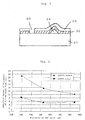
- Fig. 1 is a flowchart illustrating an example of a method of producing an SOI wafer by an ion implantation delamination method according to the present invention.
- Fig. 2 is a flowchart illustrating a conventional method of producing an SOI wafer by an ion implantation delamination method.
- Fig. 3 is a schematic explanatory diagram illustrating schematically a void and a blister generated in an SOI wafer.
- Fig. 4 is a graph illustrating the relation between heat treatment time of the heat treatment to reduce the thickness of buried oxide film and the reduction amount of the thickness of buried oxide film, and the relation between the thickness of SOI layer formed in a bonded wafer and the reduction amount of the thickness of buried oxide film.
- the inventors of the present invention have assiduously studied and discussed a method of producing an SOI wafer in which blisters and voids are not generated, the thickness of the buried oxide film is thin, and the SOI layer has good crystallinity.
- a bonding method after an oxide film is formed so that the total thickness of the oxide film formed on at least one wafer surface of two wafers is thicker than the thickness of the buried oxide film that the SOI wafer to be produced has, the wafers are bonded to each other and the bond wafer is made into a thin film to form an SOI layer, thereafter, an obtained bonded wafer is subjected to heat treatment, and thereby, the thickness of the buried oxide film can be reduced to a desired thickness of 100 nm or less without generating blisters and voids, and moreover, the SOI layer has good crystallinity.
- Fig. 1 is a flowchart illustrating an example of a method of producing an SOI wafer by an ion implantation delamination method according to the present invention.
- Step (a) two mirror-polished silicon wafers are prepared.
- one wafer is a base wafer 1 to be a supporting substrate suiting to the specification of a device and the other wafer is a bond wafer 2 to be an SOI layer.
- Step (b) at least one of the wafers, the bond wafer 2 in this case, is subjected to thermal oxidation treatment to form an oxide film 3 on the surface thereof.
- the oxide film is formed so that the thickness of the oxide film formed on the surface of the bond wafer is thicker than the thickness of a buried oxide film that the SOI wafer should finally have when the SOI wafer has been produced, for example, the oxide film is formed so as to have a thickness of 100 nm or more.
- the oxide film is formed so as to have a thickness of 100 nm or more, generation of blisters and voids can be surely prevented in subsequent delaminating heat treatment.
- a wafer on which the oxide film may be formed is not limited to the bond wafer, and the oxide film may be formed on the base wafer or both of the base wafer and the bond wafer respectively.
- the oxide films are formed so that a total thickness of the oxide films formed on the surfaces of both wafers is thicker than a desired thickness of the buried oxide film that the SOI wafer should finally have.
- an ion-implanted layer 4 parallel to a wafer surface at an average penetration depth of ion is formed by implanting hydrogen ions (H + ions, H - ions, H 2 + ions, etc.) into a surface portion of the bond wafer 2 in which the oxide film 3 is formed on its surface.
- hydrogen ions H + ions, H - ions, H 2 + ions, etc.
- rare gas ions or mixture of hydrogen ions and rare gas ions may be possible.
- Step (d) the hydrogen ion-implanted surface of the bond wafer 2 is superposed on the base wafer 1 through the oxide film 3 and brought into close contact with it.
- the wafers can be bonded to each other without using adhesive etc. by, for example, contacting the surfaces of the two wafers to each other in a clean atmosphere at the room temperature.
- Step (e) the bond wafer is made into a thin film to form an SOI layer 5.
- Making the bond wafer 2 into a thin film can be easily performed by, for example, subjecting it to delaminating heat treatment in an inert gas atmosphere at a temperature of about 500°C or more to delaminate it at the ion-implanted layer 4 formed in the bond wafer 2 by the above hydrogen ion implantation as an interface.
- the delaminating heat treatment may be omitted by subjecting the surface of the wafer before bonding to plasma treatment to make it activated, and bonding the wafers to each other.
- the SOI layer having extremely good thickness uniformity can be easily formed. Also, an SOI layer having a desired thickness can be precisely formed by a touch polishing after the bond wafer is delaminated at the ion-implanted layer.
- the SOI wafer 7 having a buried oxide film 6 of which thickness is reduced to a desired thickness can be produced.
- the thickness of the buried oxide film of the SOI wafer finally obtained depends on the product standards, however, according to the present invention, the thickness is possible to be 100 nm or less, further 50 nm or less.
- the bonded wafer after delamination is subjected directly to the heat treatment in Step (f) while omitting the touch polishing, or the touch polishing is performed after the heat treatment in Step (f).
- Conditions of the heat treatment to reduce the thickness of the buried oxide film can be determined according to demands, and they are not limited in particular.
- the heat treatment is performed in an atmosphere of a hydrogen gas, an argon gas, or a mixed gas of those at a temperature of 1000 °C or more, preferably 1100 °C or more, more preferably 1150 °C or more.
- the thickness of the buried oxide film can be effectively reduced, so that there can be easily obtained the buried oxide film having a thickness of less than 100 nm, for example, 10 - 80 nm, and there can be produced an SOI wafer in which the bonding strength between the wafers are increased, so that they are bonded strongly to each other.
- the reduction amount of the thickness of the buried oxide film in the heat treatment can be increased. It was revealed that when the thickness of the SOI layer formed on the buried oxide film is thicker than 500 nm, even if the heat treatment to reduce the thickness of the oxide film is performed, it is necessary to perform the heat treatment for a long time so as to obtain a buried oxide film having a desired thickness since the reduction amount of the thickness of the buried oxide film is small.
- the thickness of the SOI layer formed by thinning the bond wafer is 500 nm or less, and thereby, the heat treatment to reduce the thickness of the buried oxide film can be effectively performed, and the buried oxide film can be thinned to a desired thickness in a short period.
- the method of producing an SOI wafer of the present invention it is preferable that after the heat treatment to reduce the thickness of the buried oxide film is performed, a thermal oxide film is formed on the SOI layer, and the oxide film is eliminated, i.e., sacrificial oxidation treatment is performed.
- the oxide film formed on the SOI layer surface is eliminated.
- the oxide film may be eliminated by etching with an aqueous solution containing HF, for example. If the oxide film is eliminated by etching with an aqueous solution containing HF, only the oxide film is eliminated by the etching, and thus, there can be obtained an SOI wafer in which damages and contaminants such as heavy metals are eliminated by means of sacrificial oxidation.
- sacrificial oxidation treatment is further performed. Thereby, a damaged layer generated on a surface of the SOI layer due to ion implantation can be surely eliminated, and moreover, since the thickness of the SOI layer can be adjusted while further increasing the crystal quality of the SOI layer, a higher-quality SOI wafer can be produced.
- the SOI wafer is produced by the method as described above, and thereby, an SOI wafer in which generation of blisters and voids is suppressed and its buried oxide film is thinned to a desired thickness can be produced at a high yield. Also, since the thickness of the buried oxide film is reduced by the heat treatment to reduce the thickness of the buried oxide film, the portion where the thickness is decreased is deoxidized to be a silicon layer having good crystallinity, and since an SOI layer is grown by solid-phase growth from the silicon layer having good crystallinity as a seed, an SOI layer having extremely good crystallinity can be obtained.
- Mirror-polished silicon wafers having a diameter of 200 mm were prepared to produce an SOI wafer having a buried oxide film with a thickness of 80 nm as a product standard by an ion implantation delamination method.
- a silicon wafer to be a bond wafer was thermally oxidized to form an oxide film having a thickness of 100 nm on a surface of the silicon wafer
- hydrogen ions were implanted into the silicon wafer at implantation energy of 53 keV (Implantation dose: 5.5 x 10 16 /cm 2 ) to form an ion-implanted layer.
- delaminating heat treatment was performed in a nitrogen atmosphere at 500 °C for 30 minutes to delaminate the bond wafer at the ion-implanted layer, a wafer having an SOI layer was produced.
- the obtained bonded wafer was subjected to a touch polishing with a stock removal of 60 nm to form the SOI layer having a thickness of 320 nm.
- the bonded wafer was subjected to heat treatment to reduce the thickness of the buried oxide film in an argon gas atmosphere at 1200 °C for 4 hours to reduce the thickness of the buried oxide film by 20 nm, and an SOI wafer having the buried oxide film of 80 nm was produced.
- Mirror-polished silicon wafers having a diameter of 200 mm were prepared to produce an SOI wafer having a buried oxide film with a thickness of 30 nm as a product standard by an ion implantation delamination method.
- the bonded wafer was subjected to heat treatment to reduce the thickness of the buried oxide film in an argon gas atmosphere at 1200 °C for 14 hours to reduce the thickness of the buried oxide film by 70 nm, and an SOI wafer having the buried oxide film of 30 nm was produced.
- Two pairs of two mirror-polished silicon wafers having a diameter of 200 mm were prepared to produce SOI wafers having buried oxide films with a thickness of 80 nm (Comparative Example 1) and with a thickness of 30 nm (Comparative Example 2) respectively as a product standard by an ion implantation method.
- each bond wafer was bonded to each base wafer having no oxide film on the surface through the oxide film
- delaminating heat treatment was performed in a nitrogen atmosphere at 500 °C for 30 minutes to delaminate each bond wafer at the ion-implanted layer, and wafers having an SOI layers were produced.
- Each obtained bonded wafer was subjected to a touch polishing with a stock removal of 60 nm to form an SOI layer having a thickness of 320 nm.
- Example 1 Example 2 Comparative Example 1 Comparative Example 2 Thickness of formed oxide film in total 100 nm 100 nm 80 nm 30 nm Implantation energy 53 keV 50 keV 50 keV 44 keV Implantation dose (/cm 2 ) 5.5x10 16 5.5x10 16 5.5x10 16 5.5x10 16 Stock removal of touch polishing 60 nm 60 nm 60 nm 60 nm Thickness of SOI layer 320 nm 320 nm 320 nm 320 nm 320 nm Heat treatment conditions to reduce thickness of oxide film In Ar gas atmosphere at 1200°C for 4 or 14 hours Non Non Thickness of buried oxide film after heat treatment 80 nm 30 nm - - Amount of generation of voids and blisters 0 2 19 26
- bonding heat treatment to further increase the bonding strength between the bond wafer and the base wafer can be performed, and thereby, there can be obtained an SOI wafer in which the wafers are further firmly bonded to each other.
- the bond wafer is thinned by the ion implantation delamination method.
- the present invention is not limited thereto, and, for example, a grinding and polishing method or PACE method can be applied to the present invention.
Landscapes
- Element Separation (AREA)
Applications Claiming Priority (3)
| Application Number | Priority Date | Filing Date | Title |
|---|---|---|---|
| JP2003004833 | 2003-01-10 | ||
| JP2003004833A JP4407127B2 (ja) | 2003-01-10 | 2003-01-10 | Soiウエーハの製造方法 |
| PCT/JP2003/016796 WO2004064145A1 (fr) | 2003-01-10 | 2003-12-25 | Procédé de production d'une plaquette soi et plaquette soi |
Publications (2)
| Publication Number | Publication Date |
|---|---|
| EP1583145A1 true EP1583145A1 (fr) | 2005-10-05 |
| EP1583145A4 EP1583145A4 (fr) | 2008-01-02 |
Family
ID=32708980
Family Applications (1)
| Application Number | Title | Priority Date | Filing Date |
|---|---|---|---|
| EP03768276A Withdrawn EP1583145A4 (fr) | 2003-01-10 | 2003-12-25 | Procédé de production d'une plaquette soi et plaquette soi |
Country Status (5)
| Country | Link |
|---|---|
| US (1) | US20050118789A1 (fr) |
| EP (1) | EP1583145A4 (fr) |
| JP (1) | JP4407127B2 (fr) |
| TW (1) | TW200416813A (fr) |
| WO (1) | WO2004064145A1 (fr) |
Cited By (2)
| Publication number | Priority date | Publication date | Assignee | Title |
|---|---|---|---|---|
| EP1818971A4 (fr) * | 2004-11-30 | 2008-01-23 | Shinetsu Handotai Kk | Procédé servant à fabriquer une tranche à collage direct et tranche à collage direct |
| EP2128891A4 (fr) * | 2007-02-28 | 2011-07-06 | Shinetsu Chemical Co | Procédé de fabrication d'un substrat laminé et substrat laminé |
Families Citing this family (30)
| Publication number | Priority date | Publication date | Assignee | Title |
|---|---|---|---|---|
| CN1922732B (zh) * | 2004-02-25 | 2010-06-09 | S.O.I.Tec绝缘体上硅技术公司 | 光电检测装置 |
| JP5183874B2 (ja) * | 2004-12-28 | 2013-04-17 | 信越化学工業株式会社 | Soiウエーハの製造方法 |
| KR20080086893A (ko) * | 2005-12-27 | 2008-09-26 | 신에쓰 가가꾸 고교 가부시끼가이샤 | Soi 웨이퍼의 제조 방법 및 soi 웨이퍼 |
| JP2007243038A (ja) * | 2006-03-10 | 2007-09-20 | Sumco Corp | 貼り合わせウェーハ及びその製造方法 |
| JP2008016534A (ja) | 2006-07-04 | 2008-01-24 | Sumco Corp | 貼り合わせウェーハの製造方法 |
| ATE486366T1 (de) * | 2006-12-26 | 2010-11-15 | Soitec Silicon On Insulator | Verfahren zum herstellen einer halbleiter-auf- isolator-struktur |
| FR2910702B1 (fr) * | 2006-12-26 | 2009-04-03 | Soitec Silicon On Insulator | Procede de fabrication d'un substrat mixte |
| JP4820801B2 (ja) * | 2006-12-26 | 2011-11-24 | 株式会社Sumco | 貼り合わせウェーハの製造方法 |
| SG144092A1 (en) * | 2006-12-26 | 2008-07-29 | Sumco Corp | Method of manufacturing bonded wafer |
| CN101548369B (zh) * | 2006-12-26 | 2012-07-18 | 硅绝缘体技术有限公司 | 制造绝缘体上半导体结构的方法 |
| WO2008096194A1 (fr) | 2007-02-08 | 2008-08-14 | S.O.I.Tec Silicon On Insulator Technologies | Procédé de fabrication de substrats dissipant la chaleur de manière importante |
| EP2135278A1 (fr) | 2007-03-19 | 2009-12-23 | S.O.I.T.E.C. Silicon on Insulator Technologies | Silicium sur isolant mince à motifs |
| JP5135935B2 (ja) * | 2007-07-27 | 2013-02-06 | 信越半導体株式会社 | 貼り合わせウエーハの製造方法 |
| JP2011504655A (ja) * | 2007-11-23 | 2011-02-10 | エス. オー. アイ. テック シリコン オン インシュレーター テクノロジーズ | 精密な酸化物の溶解 |
| JP5466410B2 (ja) * | 2008-02-14 | 2014-04-09 | 信越化学工業株式会社 | Soi基板の表面処理方法 |
| US8148242B2 (en) * | 2008-02-20 | 2012-04-03 | Soitec | Oxidation after oxide dissolution |
| JP5263509B2 (ja) | 2008-09-19 | 2013-08-14 | 信越半導体株式会社 | 貼り合わせウェーハの製造方法 |
| FR2938118B1 (fr) | 2008-10-30 | 2011-04-22 | Soitec Silicon On Insulator | Procede de fabrication d'un empilement de couches minces semi-conductrices |
| FR2938119B1 (fr) * | 2008-10-30 | 2011-04-22 | Soitec Silicon On Insulator | Procede de detachement de couches semi-conductrices a basse temperature |
| JP5493345B2 (ja) * | 2008-12-11 | 2014-05-14 | 信越半導体株式会社 | Soiウェーハの製造方法 |
| FR2941324B1 (fr) * | 2009-01-22 | 2011-04-29 | Soitec Silicon On Insulator | Procede de dissolution de la couche d'oxyde dans la couronne d'une structure de type semi-conducteur sur isolant. |
| FR2964495A1 (fr) * | 2010-09-02 | 2012-03-09 | Soitec Silicon On Insulator | Procede de fabrication d'une structure seoi multiple comportant une couche isolante ultrafine |
| FR2972564B1 (fr) | 2011-03-08 | 2016-11-04 | S O I Tec Silicon On Insulator Tech | Procédé de traitement d'une structure de type semi-conducteur sur isolant |
| JP5802436B2 (ja) * | 2011-05-30 | 2015-10-28 | 信越半導体株式会社 | 貼り合わせウェーハの製造方法 |
| US8994085B2 (en) | 2012-01-06 | 2015-03-31 | International Business Machines Corporation | Integrated circuit including DRAM and SRAM/logic |
| US8653596B2 (en) * | 2012-01-06 | 2014-02-18 | International Business Machines Corporation | Integrated circuit including DRAM and SRAM/logic |
| FR2998418B1 (fr) | 2012-11-20 | 2014-11-21 | Soitec Silicon On Insulator | Procede de fabrication d'un substrat de type semi-conducteur sur isolant |
| JP5780234B2 (ja) | 2012-12-14 | 2015-09-16 | 信越半導体株式会社 | Soiウェーハの製造方法 |
| FR3003684B1 (fr) * | 2013-03-25 | 2015-03-27 | Soitec Silicon On Insulator | Procede de dissolution d'une couche de dioxyde de silicium. |
| FR3034565B1 (fr) | 2015-03-30 | 2017-03-31 | Soitec Silicon On Insulator | Procede de fabrication d'une structure presentant une couche dielectrique enterree d'epaisseur uniforme |
Family Cites Families (19)
| Publication number | Priority date | Publication date | Assignee | Title |
|---|---|---|---|---|
| JP3522482B2 (ja) * | 1997-02-24 | 2004-04-26 | 三菱住友シリコン株式会社 | Soi基板の製造方法 |
| FR2777115B1 (fr) * | 1998-04-07 | 2001-07-13 | Commissariat Energie Atomique | Procede de traitement de substrats semi-conducteurs et structures obtenues par ce procede |
| JPH11307472A (ja) * | 1998-04-23 | 1999-11-05 | Shin Etsu Handotai Co Ltd | 水素イオン剥離法によってsoiウエーハを製造する方法およびこの方法で製造されたsoiウエーハ |
| JP3395661B2 (ja) * | 1998-07-07 | 2003-04-14 | 信越半導体株式会社 | Soiウエーハの製造方法 |
| JP4273540B2 (ja) * | 1998-07-21 | 2009-06-03 | 株式会社Sumco | 貼り合わせ半導体基板及びその製造方法 |
| JP2000124092A (ja) * | 1998-10-16 | 2000-04-28 | Shin Etsu Handotai Co Ltd | 水素イオン注入剥離法によってsoiウエーハを製造する方法およびこの方法で製造されたsoiウエーハ |
| FR2797713B1 (fr) * | 1999-08-20 | 2002-08-02 | Soitec Silicon On Insulator | Procede de traitement de substrats pour la microelectronique et substrats obtenus par ce procede |
| EP2259299A1 (fr) * | 1999-10-14 | 2010-12-08 | Shin-Etsu Handotai Co., Ltd. | Procédé de fabrication de tranche SOI, et tranche SOI |
| EP1187216B1 (fr) * | 1999-12-24 | 2018-04-04 | Shin-Etsu Handotai Co., Ltd. | Procede de production de tranche collee |
| FR2816445B1 (fr) * | 2000-11-06 | 2003-07-25 | Commissariat Energie Atomique | Procede de fabrication d'une structure empilee comprenant une couche mince adherant a un substrat cible |
| JP2003204048A (ja) * | 2002-01-09 | 2003-07-18 | Shin Etsu Handotai Co Ltd | Soiウエーハの製造方法及びsoiウエーハ |
| KR100511656B1 (ko) * | 2002-08-10 | 2005-09-07 | 주식회사 실트론 | 나노 에스오아이 웨이퍼의 제조방법 및 그에 따라 제조된나노 에스오아이 웨이퍼 |
| US7129123B2 (en) * | 2002-08-27 | 2006-10-31 | Shin-Etsu Handotai Co., Ltd. | SOI wafer and a method for producing an SOI wafer |
| JP2004193515A (ja) * | 2002-12-13 | 2004-07-08 | Shin Etsu Handotai Co Ltd | Soiウエーハの製造方法 |
| JP2004247610A (ja) * | 2003-02-14 | 2004-09-02 | Canon Inc | 基板の製造方法 |
| US7176528B2 (en) * | 2003-02-18 | 2007-02-13 | Corning Incorporated | Glass-based SOI structures |
| FR2855908B1 (fr) * | 2003-06-06 | 2005-08-26 | Soitec Silicon On Insulator | Procede d'obtention d'une structure comprenant au moins un substrat et une couche ultramince |
| US7052978B2 (en) * | 2003-08-28 | 2006-05-30 | Intel Corporation | Arrangements incorporating laser-induced cleaving |
| US7018484B1 (en) * | 2005-02-09 | 2006-03-28 | Translucent Inc. | Semiconductor-on-insulator silicon wafer and method of formation |
-
2003
- 2003-01-10 JP JP2003004833A patent/JP4407127B2/ja not_active Expired - Fee Related
- 2003-12-25 EP EP03768276A patent/EP1583145A4/fr not_active Withdrawn
- 2003-12-25 US US10/507,175 patent/US20050118789A1/en not_active Abandoned
- 2003-12-25 WO PCT/JP2003/016796 patent/WO2004064145A1/fr not_active Ceased
-
2004
- 2004-01-07 TW TW093100368A patent/TW200416813A/zh not_active IP Right Cessation
Cited By (4)
| Publication number | Priority date | Publication date | Assignee | Title |
|---|---|---|---|---|
| EP1818971A4 (fr) * | 2004-11-30 | 2008-01-23 | Shinetsu Handotai Kk | Procédé servant à fabriquer une tranche à collage direct et tranche à collage direct |
| US7521334B2 (en) | 2004-11-30 | 2009-04-21 | Shin-Etsu Handotai Co., Ltd. | Method for producing direct bonded wafer and direct bonded wafer |
| EP2128891A4 (fr) * | 2007-02-28 | 2011-07-06 | Shinetsu Chemical Co | Procédé de fabrication d'un substrat laminé et substrat laminé |
| US8765576B2 (en) | 2007-02-28 | 2014-07-01 | Shin-Etsu Chemical Co., Ltd. | Process for producing laminated substrate and laminated substrate |
Also Published As
| Publication number | Publication date |
|---|---|
| EP1583145A4 (fr) | 2008-01-02 |
| US20050118789A1 (en) | 2005-06-02 |
| TW200416813A (en) | 2004-09-01 |
| WO2004064145A1 (fr) | 2004-07-29 |
| JP2004221198A (ja) | 2004-08-05 |
| TWI310962B (fr) | 2009-06-11 |
| JP4407127B2 (ja) | 2010-02-03 |
Similar Documents
| Publication | Publication Date | Title |
|---|---|---|
| EP1583145A1 (fr) | Procédé de production d'une plaquette soi et plaquette soi | |
| US7091107B2 (en) | Method for producing SOI wafer and SOI wafer | |
| US10475694B2 (en) | Handle substrate for use in manufacture of semiconductor-on-insulator structure and method of manufacturing thereof | |
| KR100614120B1 (ko) | Soi웨이퍼의 제조방법 및 이 방법으로 제조된 soi웨이퍼 | |
| EP1408551B1 (fr) | Procede de production de plaquettes de liaison | |
| EP1453096B1 (fr) | Procédé de fabrication d'une plaquette liée | |
| KR101035699B1 (ko) | 전자 공학, 광학 또는 광전자 공학용의 2개 기판의 직접본딩 방법 | |
| US8236667B2 (en) | Silicon on insulator (SOI) wafer and process for producing same | |
| US7276427B2 (en) | Method for manufacturing SOI wafer | |
| KR20030089712A (ko) | Soi 웨이퍼 및 그 제조방법 | |
| EP1863083A2 (fr) | Procédé de production d'un substrat à semi-conducteur | |
| KR102562239B1 (ko) | 반도체 도너 기판으로부터의 층 전이를 용이하게 하는 광 지원형 소판 형성 | |
| KR20070055382A (ko) | 접합웨이퍼의 제조방법 | |
| JP2011054704A (ja) | 貼り合わせウェーハの製造方法 | |
| JP2007317878A (ja) | 半導体基板の製造方法 | |
| JP5364345B2 (ja) | Soi基板の作製方法 | |
| EP1901340A1 (fr) | Procédé de production de plaquette fixée | |
| JP4730645B2 (ja) | Soiウェーハの製造方法 | |
| JP5135713B2 (ja) | 半導体基板の製造方法 | |
| JP2006013179A (ja) | Soiウェーハの製造方法 |
Legal Events
| Date | Code | Title | Description |
|---|---|---|---|
| PUAI | Public reference made under article 153(3) epc to a published international application that has entered the european phase |
Free format text: ORIGINAL CODE: 0009012 |
|
| 17P | Request for examination filed |
Effective date: 20040923 |
|
| AK | Designated contracting states |
Kind code of ref document: A1 Designated state(s): AT BE BG CH CY CZ DE DK EE ES FI FR GB GR HU IE IT LI LU MC NL PT RO SE SI SK TR |
|
| RBV | Designated contracting states (corrected) |
Designated state(s): DE FR |
|
| A4 | Supplementary search report drawn up and despatched |
Effective date: 20071203 |
|
| 17Q | First examination report despatched |
Effective date: 20080403 |
|
| RAP1 | Party data changed (applicant data changed or rights of an application transferred) |
Owner name: SHIN-ETSU HANDOTAI CO., LTD. |
|
| STAA | Information on the status of an ep patent application or granted ep patent |
Free format text: STATUS: THE APPLICATION IS DEEMED TO BE WITHDRAWN |
|
| 18D | Application deemed to be withdrawn |
Effective date: 20100701 |