EP1519641A2 - Module et procédé de fabrication d'un module - Google Patents
Module et procédé de fabrication d'un module Download PDFInfo
- Publication number
- EP1519641A2 EP1519641A2 EP04022953A EP04022953A EP1519641A2 EP 1519641 A2 EP1519641 A2 EP 1519641A2 EP 04022953 A EP04022953 A EP 04022953A EP 04022953 A EP04022953 A EP 04022953A EP 1519641 A2 EP1519641 A2 EP 1519641A2
- Authority
- EP
- European Patent Office
- Prior art keywords
- green sheet
- ceramic green
- ceramic
- electrode
- recess
- Prior art date
- Legal status (The legal status is an assumption and is not a legal conclusion. Google has not performed a legal analysis and makes no representation as to the accuracy of the status listed.)
- Granted
Links
Images


Classifications
-
- H10W90/00—
-
- H—ELECTRICITY
- H03—ELECTRONIC CIRCUITRY
- H03H—IMPEDANCE NETWORKS, e.g. RESONANT CIRCUITS; RESONATORS
- H03H9/00—Networks comprising electromechanical or electro-acoustic elements; Electromechanical resonators
- H03H9/02—Details
- H03H9/05—Holders or supports
- H03H9/0538—Constructional combinations of supports or holders with electromechanical or other electronic elements
- H03H9/0542—Constructional combinations of supports or holders with electromechanical or other electronic elements consisting of a lateral arrangement
-
- H—ELECTRICITY
- H03—ELECTRONIC CIRCUITRY
- H03H—IMPEDANCE NETWORKS, e.g. RESONANT CIRCUITS; RESONATORS
- H03H9/00—Networks comprising electromechanical or electro-acoustic elements; Electromechanical resonators
- H03H9/02—Details
- H03H9/05—Holders or supports
- H03H9/0538—Constructional combinations of supports or holders with electromechanical or other electronic elements
- H03H9/0547—Constructional combinations of supports or holders with electromechanical or other electronic elements consisting of a vertical arrangement
- H03H9/0557—Constructional combinations of supports or holders with electromechanical or other electronic elements consisting of a vertical arrangement the other elements being buried in the substrate
-
- H—ELECTRICITY
- H03—ELECTRONIC CIRCUITRY
- H03H—IMPEDANCE NETWORKS, e.g. RESONANT CIRCUITS; RESONATORS
- H03H9/00—Networks comprising electromechanical or electro-acoustic elements; Electromechanical resonators
- H03H9/02—Details
- H03H9/05—Holders or supports
- H03H9/10—Mounting in enclosures
- H03H9/1064—Mounting in enclosures for surface acoustic wave [SAW] devices
- H03H9/1085—Mounting in enclosures for surface acoustic wave [SAW] devices the enclosure being defined by a non-uniform sealing mass covering the non-active sides of the SAW device
-
- H—ELECTRICITY
- H05—ELECTRIC TECHNIQUES NOT OTHERWISE PROVIDED FOR
- H05K—PRINTED CIRCUITS; CASINGS OR CONSTRUCTIONAL DETAILS OF ELECTRIC APPARATUS; MANUFACTURE OF ASSEMBLAGES OF ELECTRICAL COMPONENTS
- H05K3/00—Apparatus or processes for manufacturing printed circuits
- H05K3/22—Secondary treatment of printed circuits
- H05K3/28—Applying non-metallic protective coatings
- H05K3/284—Applying non-metallic protective coatings for encapsulating mounted components
-
- H—ELECTRICITY
- H05—ELECTRIC TECHNIQUES NOT OTHERWISE PROVIDED FOR
- H05K—PRINTED CIRCUITS; CASINGS OR CONSTRUCTIONAL DETAILS OF ELECTRIC APPARATUS; MANUFACTURE OF ASSEMBLAGES OF ELECTRICAL COMPONENTS
- H05K3/00—Apparatus or processes for manufacturing printed circuits
- H05K3/30—Assembling printed circuits with electric components, e.g. with resistor
- H05K3/303—Surface mounted components, e.g. affixing before soldering, aligning means, spacing means
- H05K3/305—Affixing by adhesive
-
- H10W70/05—
-
- H10W70/68—
-
- H10W70/685—
-
- H10W74/012—
-
- H10W74/15—
-
- H—ELECTRICITY
- H05—ELECTRIC TECHNIQUES NOT OTHERWISE PROVIDED FOR
- H05K—PRINTED CIRCUITS; CASINGS OR CONSTRUCTIONAL DETAILS OF ELECTRIC APPARATUS; MANUFACTURE OF ASSEMBLAGES OF ELECTRICAL COMPONENTS
- H05K1/00—Printed circuits
- H05K1/02—Details
- H05K1/03—Use of materials for the substrate
- H05K1/0306—Inorganic insulating substrates, e.g. ceramic, glass
-
- H—ELECTRICITY
- H05—ELECTRIC TECHNIQUES NOT OTHERWISE PROVIDED FOR
- H05K—PRINTED CIRCUITS; CASINGS OR CONSTRUCTIONAL DETAILS OF ELECTRIC APPARATUS; MANUFACTURE OF ASSEMBLAGES OF ELECTRICAL COMPONENTS
- H05K2201/00—Indexing scheme relating to printed circuits covered by H05K1/00
- H05K2201/09—Shape and layout
- H05K2201/09009—Substrate related
- H05K2201/09036—Recesses or grooves in insulating substrate
-
- H—ELECTRICITY
- H05—ELECTRIC TECHNIQUES NOT OTHERWISE PROVIDED FOR
- H05K—PRINTED CIRCUITS; CASINGS OR CONSTRUCTIONAL DETAILS OF ELECTRIC APPARATUS; MANUFACTURE OF ASSEMBLAGES OF ELECTRICAL COMPONENTS
- H05K2201/00—Indexing scheme relating to printed circuits covered by H05K1/00
- H05K2201/10—Details of components or other objects attached to or integrated in a printed circuit board
- H05K2201/10613—Details of electrical connections of non-printed components, e.g. special leads
- H05K2201/10621—Components characterised by their electrical contacts
- H05K2201/10636—Leadless chip, e.g. chip capacitor or resistor
-
- H—ELECTRICITY
- H05—ELECTRIC TECHNIQUES NOT OTHERWISE PROVIDED FOR
- H05K—PRINTED CIRCUITS; CASINGS OR CONSTRUCTIONAL DETAILS OF ELECTRIC APPARATUS; MANUFACTURE OF ASSEMBLAGES OF ELECTRICAL COMPONENTS
- H05K2201/00—Indexing scheme relating to printed circuits covered by H05K1/00
- H05K2201/10—Details of components or other objects attached to or integrated in a printed circuit board
- H05K2201/10613—Details of electrical connections of non-printed components, e.g. special leads
- H05K2201/10621—Components characterised by their electrical contacts
- H05K2201/10674—Flip chip
-
- H10W70/63—
-
- H10W70/681—
-
- H10W72/07236—
-
- H10W72/856—
-
- H10W72/923—
-
- H10W72/9415—
-
- H10W74/00—
-
- H10W74/114—
-
- H10W90/724—
-
- H10W90/734—
-
- Y—GENERAL TAGGING OF NEW TECHNOLOGICAL DEVELOPMENTS; GENERAL TAGGING OF CROSS-SECTIONAL TECHNOLOGIES SPANNING OVER SEVERAL SECTIONS OF THE IPC; TECHNICAL SUBJECTS COVERED BY FORMER USPC CROSS-REFERENCE ART COLLECTIONS [XRACs] AND DIGESTS
- Y02—TECHNOLOGIES OR APPLICATIONS FOR MITIGATION OR ADAPTATION AGAINST CLIMATE CHANGE
- Y02P—CLIMATE CHANGE MITIGATION TECHNOLOGIES IN THE PRODUCTION OR PROCESSING OF GOODS
- Y02P70/00—Climate change mitigation technologies in the production process for final industrial or consumer products
- Y02P70/50—Manufacturing or production processes characterised by the final manufactured product
-
- Y—GENERAL TAGGING OF NEW TECHNOLOGICAL DEVELOPMENTS; GENERAL TAGGING OF CROSS-SECTIONAL TECHNOLOGIES SPANNING OVER SEVERAL SECTIONS OF THE IPC; TECHNICAL SUBJECTS COVERED BY FORMER USPC CROSS-REFERENCE ART COLLECTIONS [XRACs] AND DIGESTS
- Y10—TECHNICAL SUBJECTS COVERED BY FORMER USPC
- Y10T—TECHNICAL SUBJECTS COVERED BY FORMER US CLASSIFICATION
- Y10T29/00—Metal working
- Y10T29/43—Electric condenser making
- Y10T29/435—Solid dielectric type
-
- Y—GENERAL TAGGING OF NEW TECHNOLOGICAL DEVELOPMENTS; GENERAL TAGGING OF CROSS-SECTIONAL TECHNOLOGIES SPANNING OVER SEVERAL SECTIONS OF THE IPC; TECHNICAL SUBJECTS COVERED BY FORMER USPC CROSS-REFERENCE ART COLLECTIONS [XRACs] AND DIGESTS
- Y10—TECHNICAL SUBJECTS COVERED BY FORMER USPC
- Y10T—TECHNICAL SUBJECTS COVERED BY FORMER US CLASSIFICATION
- Y10T29/00—Metal working
- Y10T29/49—Method of mechanical manufacture
- Y10T29/49002—Electrical device making
- Y10T29/49117—Conductor or circuit manufacturing
- Y10T29/49124—On flat or curved insulated base, e.g., printed circuit, etc.
- Y10T29/49126—Assembling bases
-
- Y—GENERAL TAGGING OF NEW TECHNOLOGICAL DEVELOPMENTS; GENERAL TAGGING OF CROSS-SECTIONAL TECHNOLOGIES SPANNING OVER SEVERAL SECTIONS OF THE IPC; TECHNICAL SUBJECTS COVERED BY FORMER USPC CROSS-REFERENCE ART COLLECTIONS [XRACs] AND DIGESTS
- Y10—TECHNICAL SUBJECTS COVERED BY FORMER USPC
- Y10T—TECHNICAL SUBJECTS COVERED BY FORMER US CLASSIFICATION
- Y10T29/00—Metal working
- Y10T29/49—Method of mechanical manufacture
- Y10T29/49002—Electrical device making
- Y10T29/49117—Conductor or circuit manufacturing
- Y10T29/49124—On flat or curved insulated base, e.g., printed circuit, etc.
- Y10T29/49155—Manufacturing circuit on or in base
- Y10T29/49163—Manufacturing circuit on or in base with sintering of base
-
- Y—GENERAL TAGGING OF NEW TECHNOLOGICAL DEVELOPMENTS; GENERAL TAGGING OF CROSS-SECTIONAL TECHNOLOGIES SPANNING OVER SEVERAL SECTIONS OF THE IPC; TECHNICAL SUBJECTS COVERED BY FORMER USPC CROSS-REFERENCE ART COLLECTIONS [XRACs] AND DIGESTS
- Y10—TECHNICAL SUBJECTS COVERED BY FORMER USPC
- Y10T—TECHNICAL SUBJECTS COVERED BY FORMER US CLASSIFICATION
- Y10T29/00—Metal working
- Y10T29/49—Method of mechanical manufacture
- Y10T29/49002—Electrical device making
- Y10T29/49117—Conductor or circuit manufacturing
- Y10T29/49124—On flat or curved insulated base, e.g., printed circuit, etc.
- Y10T29/49155—Manufacturing circuit on or in base
- Y10T29/49165—Manufacturing circuit on or in base by forming conductive walled aperture in base
-
- Y—GENERAL TAGGING OF NEW TECHNOLOGICAL DEVELOPMENTS; GENERAL TAGGING OF CROSS-SECTIONAL TECHNOLOGIES SPANNING OVER SEVERAL SECTIONS OF THE IPC; TECHNICAL SUBJECTS COVERED BY FORMER USPC CROSS-REFERENCE ART COLLECTIONS [XRACs] AND DIGESTS
- Y10—TECHNICAL SUBJECTS COVERED BY FORMER USPC
- Y10T—TECHNICAL SUBJECTS COVERED BY FORMER US CLASSIFICATION
- Y10T29/00—Metal working
- Y10T29/49—Method of mechanical manufacture
- Y10T29/49002—Electrical device making
- Y10T29/49117—Conductor or circuit manufacturing
- Y10T29/49169—Assembling electrical component directly to terminal or elongated conductor
- Y10T29/49171—Assembling electrical component directly to terminal or elongated conductor with encapsulating
Definitions
- the present invention relates to a module including a ceramic substrate having a wiring pattern thereon, and electronic components, such as ICs, SAW filters, resistors, capacitors, and coils, mounted on the ceramic substrate, and to a method of manufacturing the module.
- electronic components such as ICs, SAW filters, resistors, capacitors, and coils
- Ceramic modules including electronic components, such as ICs, SAW filters, resistors, capacitors, and coils, mounted on a ceramic substrate having a wiring pattern thereon is disclosed in Japanese Patent Laid-Open Publication Nos.3-205857 and 4-252041.
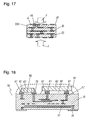
- Fig. 18 is a cross sectional view of a conventional ceramic module 50.
- the ceramic module 50 includes a component 60, such as a capacitor and an inductor, an active component 80, such as an IC and a SAW filter, and a ceramic substrate 70.
- the ceramic substrate 70 includes internal electrodes 51, via electrodes 52 connecting between the internal electrodes 51, land electrodes 55 connected with the active component 80 and the component 60 for surface-mounting them, and back electrodes 56 for mounting the ceramic module 50 on a mother board.
- the end electrodes 62 of the component 60 are connected to land electrodes 55 corresponding to them with a conductive adhesive 61, such as solder, while the back electrodes 81 of the active component 80 are connected to land electrodes 55 corresponding to them with a conductive adhesive 61.
- a gap between the active component 80 and the substrate 70 is filled with a resin 90 for increasing reliability of surface mounting of the active component 80.
- the component 60 and the active component 80 are mounted on the ceramic substrate 70 which has been baked, and may be molded with a resin 91 according to requirement.
- the conventional module 50 includes a small amount of the conductive adhesive 61 for avoiding short-circuit between the electrodes during the surface mounting.
- the resin 91 may fail to flow into beneath the component 60, and may produce a gap 92.
- the conductive adhesive 61 such as solder, may melt and flow into the gap 92 between the component 60 and the ceramic substrate 70, hence causing a short-circuit between the land electrodes 55 and disturbing the performance and the operational reliability of the ceramic module 50.
- the resin 90 is also applied to between the component 80 and the substrate 70 for mounting and securing the component 80 onto the substrate 70.
- the resin 90 upon not being applied sufficiently between the component 80 and the substrate 70, may reduce the bonding strength and the operational reliability.
- a module includes a ceramic substrate, first and second electrodes provided on the ceramic substrate, a component having third and fourth electrodes connected to the first and second electrodes, respectively, and a resin filled in a space between the component and the ceramic substrate.
- the ceramic substrate has a surface thereof having a recess formed therein.
- the first and second electrodes are provided on the surface of the ceramic substrate so that the recess is located between the first and second electrodes.
- the component is located over the recess and spaced from the ceramic substrate with a space including the recess. The space including the recess is filled with the resin.
- the module allows each component to be surface mounted at higher bonding strength, thus preventing short-circuit between the electrodes on the substrate and improving the operation reliability.
- Fig. 1 is a cross sectional view of a ceramic module 1 according to an exemplary embodiment of the present invention.
- Fig. 2 is an upper view of a ceramic substrate 13 of the module 1.
- the ceramic module 1 includes the ceramic substrate 13.
- the ceramic substrate 13 includes internal electrodes 2 provided as layers, via-electrodes 3 connecting between the internal electrodes 2, and a ceramic base 14 made of electrically-insulating material.
- a component 6, such as a chip resistor, a multi-layer ceramic capacitor, and a chip inductor, includes a main body 6A and end electrodes 15.
- the end electrode 15 and the bump electrodes 16 are connected by solders 7 to land electrodes 4, and the components 6 and 8 are provided on the upper surface 13A of the substrate 13.
- Back electrodes 5 are provided on the lower surface 13B of the ceramic substrate 13 for allowing the ceramic module 1 to be mounted on a mother board 40.
- the ceramic substrate 13 has a recess 10B in a portion of the surface of substrate 13 facing the component 6, and has a recess 10A in a portion of the surface of substrate 13 facing the component 8.
- the component 6 and the active component 8 are encapsulated with a resin molding 12 on the upper surface 13A of the ceramic substrate 13 having the components 6 and 9 mounted thereon.
- the electrodes 2 and the via-electrodes 3 in the ceramic substrate 13 are baked simultaneously together with the ceramic substrate 13 and are conductive, the electrodes are made of Ag paste having a large conductivity.
- the ceramic base 14 of the ceramic substrate 13 including the internal electrodes 2 of Ag is preferably baked substantially at 900°C.
- the ceramic base 14 may be made preferably of glass-ceramic mixture of Al 2 O 3 and glass.
- the materials of the internal electrodes 2 and the ceramic substrate 13 are not limited to the foregoing materials.
- the resin molding 12 is made of electrically-insulating resin material, such as epoxy, phenol, or epoxy-silicone resin, and secures a bonding strength and a resistance against impact of the components 6 and 8 in the module 1.
- the solders 7 may be replaced by electrically-conductive adhesives made of conductive resin.
- the component 6 and the active component 8 are mounted and electrically connected on the ceramic substrate 13. After the component 6 is placed on the ceramic substrate 13 and connected to the land electrodes 4, the space 10C including the recess 10B between the component 6 and the ceramic substrate 13 is filled with the resin 11.
- the recess 10B enables the resin 11 to be easily filled between the component 6 and the ceramic substrate 13. This arrangement produces no gap between the component 6 and the ceramic substrate 13, and the solders 7 can be prevented from flowing when the solders are heated while the module 1 is mounted on the mother board 40, thus preventing the electrodes 4 from short-circuit. Particularly if the component 6 has such a small size that the electrodes 4 is spaced a little from each other, the recess 10B is useful for receiving the resin 11.
- the resin 9 of insulating resin material such as epoxy resin
- the resin 9 may be made of material selected from various resins.
- the recess 10A allows the resin 9 to be filled between the component 8 and the substrate 13 even if the distance between the component 8 and the substrate 13 is small. This arrangement produces no gap between the component 8 and the substrate 13, hence providing the ceramic module 1 with large bonding strength and reliability for the surface mounting.
- a distance W1 between the land electrodes 4 of the component 6 or 8 and a distance W2 of the recess 10B or 10A satisfy W1 ⁇ W2 as shown in Fig. 2, and depths of the recess 10B and 10A are preferably not smaller than 10 ⁇ m.
- This arrangement prevents the solders or the conductive adhesive for mounting the component 6 or 8 on the substrate 13 from causing short-circuit between the electrodes 4 due to the flowing of the solder or adhesive, and prevents the resin 11 and 9 from being applied with insufficient amounts beneath the component 6 or 8. Accordingly, the ceramic module 1 has large bonding strength and reliability for the surface mounting of the components 6 and 8.
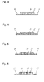
- Figs. 3 to 13 are cross sectional views of the ceramic substrate 13 for illustrating a procedure of manufacturing the substrate 13.
- the ceramic substrate 13 is formed by baking a green sheet of glass ceramic material, such as mixture of Al 2 O 3 and glass powder.
- the glass powder is preferably selected from SiO 2 , B 2 O 3 , Al 2 O 3 , CaCO 3 , SrCO 3 , SrCO 3 , BaCO 3 , La 2 O 3 , ZrO 2 , TiO 2 , MgO, PbO, ZnO, Li 2 O 3 , Na 2 CO 3 , and K 2 CO 3 .
- the mixture of Al 2 O 3 and glass powder is added with poly vinyl butylal binder, plasticizer, and organic solvent for dispersion, thus providing slurry.
- the above described composition is illustrative, and may be replaced with any other appropriate example for providing slurry.
- the slurry is applied on a base film 21 made of, for example, PET material with a doctor blade or the like, and is dried, thus providing a ceramic green sheet 20 having predetermined desired thickness and size, as shown in Fig. 3.
- the base film 21 is not limited to the PET material but may be made of any other appropriate material.
- the green sheet 20 is perforated by punching or laser beam machining to have through-holes 22 formed therein, as shown in Fig. 4. Pilot holes 27 may be provided in the base film 21 for multi-layer assembly if necessary.
- the through-holes 22 are then filled with silver paste to develop via-electrodes 23, as shown in Fig. 5.
- a pattern of the internal electrodes 24 are formed by, for example, screen printing, as shown in Fig. 6.
- the internal electrodes 24 are patterned with paste made of Ag-based conductive material, however the paste may be made of any conductive material other than the Ag-based material which can be baked simultaneously with the green sheet 20.
- the base films 21 having green sheets 20A-20D, the via electrodes 23, and the internal electrodes 24 are aligned by inserting guide pins through the pilot holes 27, as shown in Fig. 7. Then, the green sheet 20A is placed on a stack pallet 25. Then, the green sheet 20B is placed on the green sheet 20A on the stack pallet 25 while pilot holes 27 aligned with the guide pins 26 inserted. Then, similarly, the green sheet 20C is stacked on the green sheet 20B, and the green sheet 20D is stacked on the green sheet 20C.
- a multi-layer block 28 including the green sheets 20A-20D is provided, as shown in Fig. 8.
- the land electrodes 4 are provided on the upper surface of the multi-layer block 28.
- the pilot holes 27 are provided in the base film 21 according to the embodiment, however, may be provided in the green sheets 20A-20D. Then, pressures F are applied to the multi-layer block 28 for having the green sheets 20A-20D have an uniform density and for eliminating de-lamination between any adjacent ones of the green sheets 20A-20D. Accordingly, the green sheets 20A-20D are pressed and joined together.
- the multi-layer block 28 is then degreased at a temperature ranging from 350°C to 600°C, and baked at a temperature ranging from 850°C to 950°C, hence providing the ceramic substrate 13 including the internal electrodes 24 of the Ag-based material, as shown in Fig. 9.
- a recess 30 is formed by applying laser beam 29 at a portion of the ceramic substrate 13 between the land electrodes 4, as shown in Fig. 10.
- the laser beam 29 forms the recess 30 in a short period of time.
- the end electrodes 15 of the component 6 are connected to the electrodes 4 with solders 7. Then, the recess 30 is filled with the resin 11, such as epoxy resin or silicone resin, and the resin 11 is cured. This allows the resin 11 filled in the recess 30 to prevents short-circuit between the electrodes 4 since the resin prevents the solders 7 from flowing between the electrodes 4 when being heated for mounting another component on the substrate 13 at a succeeding step.
- the resin 11 such as epoxy resin or silicone resin
- a recess 30 is formed at beneath the component 8 and in the substrate 13, and filled with the resin 9 for improving the bonding strength and reliability of the mounting.
- This arrangement allows the resin 9 to be filled and cured between the component 8 and the substrate 13 with producing of no gap, hence contributing to the improvement in the bonding strength and operational reliability of the ceramic module 1.
- a land electrode 4A having a large size may be formed on the ceramic substrate 13, and is then baked. Then, the land electrode 4A is divided into the electrodes 4 at the same time when the recess 30 is formed by the laser beam 29 in the substrate 13, as shown in Fig. 12. That is, the electrodes 4 and the recess 30 can be formed simultaneously. This operation allows the recess 30 to be formed precisely between the land electrodes 4 without consideration of thinning of the conductive paste or accuracy of the patterning even when the land electrodes 4 have small sizes.
- the component 6 and the active component 8 (not shown) are mounted while the resin 11 is filled in the recess 30 as well as beneath the component 6, as shown in Fig. 13. They are molded with a resin molding 12 and cut by dicing into the ceramic modules 1 having a predetermined size.
- the electrodes 4 and 4A may be baked together with the ceramic substrate 13 or after the ceramic substrate 13 is baked.
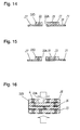
- Figs. 14 to 16 are cross sectional views of the ceramic module for illustrating another method for manufacturing the module according to the embodiment.
- a though-hole 22A may be formed in the green sheet 20D, which is to be placed at the outermost layer, at a portion where the recesses 10A and 10B is to be provided, as shown in Fig. 14.
- the via-electrodes 23 is formed in the through-holes 22, as shown in Fig. 15, and the internal electrodes 24 are formed, as shown in Fig. 16.
- the green sheets 20A-20D are stacked and baked.
- the through-hole 22A serves as the recesses 10A and 10B in the multi-layer block 28.
- the components 6 and 8 are mounted, as shown in Fig. 13, and the resins 9 and 10 are then applied. Finally, they are encapsulated in the resin molding 12, thus providing the ceramic module 1.
- the recesses 10A and 10B can be provided without forming recesses after the green sheets 20A-20D are baked.
- the recess 30 may be formed in the multi-layer block 28 by laser beam machining before the block is baked. After the baking of the multi-layer block 28, the components 6 and 8 are mounted, the resins 9 and 11 are applied, and the resin molding 12 is provided, thus providing the ceramic module 1.
- the recess 30 between the land electrodes 4 may be formed by locating a die 41 between the land electrodes 4 and pressing the die downwardly while the multi-layer block 28 is pressed.
- the recess 30 may be formed by laser beam between the land electrodes 4. The recess 30 can be formed before and after the pressing of the block. After the baking of the multi-layer block 28, the components 6 and 8 are mounted, the resins 9 and 11 are applied, and the resin molding 12 is formed, thus providing the ceramic module 1 having the recesses 10A and 10B between the land electrodes 4 readily and easily.
Landscapes
- Engineering & Computer Science (AREA)
- Physics & Mathematics (AREA)
- Acoustics & Sound (AREA)
- Manufacturing & Machinery (AREA)
- Microelectronics & Electronic Packaging (AREA)
- Structures For Mounting Electric Components On Printed Circuit Boards (AREA)
- Fixed Capacitors And Capacitor Manufacturing Machines (AREA)
- Printing Elements For Providing Electric Connections Between Printed Circuits (AREA)
- Production Of Multi-Layered Print Wiring Board (AREA)
- Non-Metallic Protective Coatings For Printed Circuits (AREA)
- Structures Or Materials For Encapsulating Or Coating Semiconductor Devices Or Solid State Devices (AREA)
Applications Claiming Priority (2)
| Application Number | Priority Date | Filing Date | Title |
|---|---|---|---|
| JP2003337180 | 2003-09-29 | ||
| JP2003337180A JP2005108950A (ja) | 2003-09-29 | 2003-09-29 | セラミックモジュール部品およびその製造方法 |
Publications (3)
| Publication Number | Publication Date |
|---|---|
| EP1519641A2 true EP1519641A2 (fr) | 2005-03-30 |
| EP1519641A3 EP1519641A3 (fr) | 2005-08-24 |
| EP1519641B1 EP1519641B1 (fr) | 2010-11-17 |
Family
ID=34191559
Family Applications (1)
| Application Number | Title | Priority Date | Filing Date |
|---|---|---|---|
| EP04022953A Expired - Lifetime EP1519641B1 (fr) | 2003-09-29 | 2004-09-27 | Module et procédé de fabrication d'un module |
Country Status (5)
| Country | Link |
|---|---|
| US (1) | US7231712B2 (fr) |
| EP (1) | EP1519641B1 (fr) |
| JP (1) | JP2005108950A (fr) |
| CN (1) | CN100369532C (fr) |
| DE (1) | DE602004030081D1 (fr) |
Cited By (1)
| Publication number | Priority date | Publication date | Assignee | Title |
|---|---|---|---|---|
| EP1628509A3 (fr) * | 2004-08-16 | 2006-10-04 | Delphi Technologies, Inc. | Module électronique avec support formé in situ |
Families Citing this family (19)
| Publication number | Priority date | Publication date | Assignee | Title |
|---|---|---|---|---|
| EP1855516A4 (fr) * | 2005-03-04 | 2010-07-28 | Murata Manufacturing Co | Plaquette ceramique multicouche et son procede de fabrication |
| JP4145902B2 (ja) * | 2005-07-19 | 2008-09-03 | セイコーエプソン株式会社 | 半導体装置及びその製造方法 |
| KR100902685B1 (ko) * | 2005-11-02 | 2009-06-15 | 파나소닉 주식회사 | 전자 부품 패키지 |
| JP4946565B2 (ja) * | 2007-03-27 | 2012-06-06 | 株式会社デンソー | モールドパッケージおよびその製造方法 |
| KR101011199B1 (ko) * | 2007-11-01 | 2011-01-26 | 파나소닉 주식회사 | 실장 구조체 |
| JP2011100718A (ja) * | 2009-10-05 | 2011-05-19 | Yazaki Corp | コネクタ |
| JP5711472B2 (ja) * | 2010-06-09 | 2015-04-30 | 新光電気工業株式会社 | 配線基板及びその製造方法並びに半導体装置 |
| JP5772970B2 (ja) * | 2011-10-21 | 2015-09-02 | 株式会社村田製作所 | 多層配線基板、プローブカード及び多層配線基板の製造方法 |
| TWI527505B (zh) | 2013-01-10 | 2016-03-21 | 元太科技工業股份有限公司 | 電路基板結構及其製造方法 |
| WO2014156393A1 (fr) | 2013-03-27 | 2014-10-02 | 株式会社村田製作所 | Pâte de céramique isolante, composant électronique en céramique et son procédé de production |
| WO2015170539A1 (fr) | 2014-05-08 | 2015-11-12 | 株式会社村田製作所 | Substrat multicouche en résine et procédé de fabrication correspondant |
| US9902006B2 (en) | 2014-07-25 | 2018-02-27 | Raytheon Company | Apparatus for cleaning an electronic circuit board |
| JP6460124B2 (ja) * | 2014-12-17 | 2019-01-30 | 株式会社村田製作所 | 積層セラミック電子部品およびその製造方法 |
| JP6589301B2 (ja) * | 2015-03-10 | 2019-10-16 | セイコーエプソン株式会社 | 液体噴射ヘッド、及び液体噴射ヘッドの製造方法 |
| WO2017077837A1 (fr) * | 2015-11-05 | 2017-05-11 | 株式会社村田製作所 | Substrat à composant monté |
| TWI562410B (en) * | 2015-12-02 | 2016-12-11 | Kaistar Lighting Xiamen Co Ltd | Packaging Substrate and LED Flip Chip Packaging structure |
| CN105428508B (zh) | 2015-12-02 | 2018-08-24 | 开发晶照明(厦门)有限公司 | 封装基板以及led倒装封装结构 |
| EP3468312B1 (fr) * | 2017-10-06 | 2023-11-29 | AT & S Austria Technologie & Systemtechnik Aktiengesellschaft | Procédé de fabrication d'un support de composants avec une structure de câblage imprimée en trois dimensions |
| JP7632173B2 (ja) * | 2021-08-24 | 2025-02-19 | トヨタ紡織株式会社 | 樹脂封止型電子基板および樹脂封止型電子基板の製造方法 |
Family Cites Families (16)
| Publication number | Priority date | Publication date | Assignee | Title |
|---|---|---|---|---|
| JPH01303791A (ja) * | 1988-05-31 | 1989-12-07 | Aisin Seiki Co Ltd | 印刷配線基板及び印刷配線基板樹脂封止時の気泡発生防止方法 |
| JPH03205857A (ja) | 1990-01-06 | 1991-09-09 | Fujitsu Ltd | 樹脂封止型電子部品 |
| JPH0483392A (ja) * | 1990-07-25 | 1992-03-17 | Narumi China Corp | 電子用セラミック基板の製造方法 |
| JPH04252041A (ja) | 1991-01-28 | 1992-09-08 | Nec Corp | 混成集積回路の製造方法 |
| JP2945291B2 (ja) * | 1994-12-27 | 1999-09-06 | 株式会社住友金属エレクトロデバイス | セラミック多層基板 |
| JP3648277B2 (ja) * | 1995-01-12 | 2005-05-18 | 株式会社東芝 | 半導体装置 |
| JPH10233463A (ja) * | 1997-01-27 | 1998-09-02 | Toshiba Corp | 半導体装置およびその製造方法 |
| DE19729073A1 (de) * | 1997-07-08 | 1999-01-14 | Bosch Gmbh Robert | Verfahren zur Herstellung einer Klebeverbindung zwischen einem elektronischen Bauelement und einem Trägersubstrat |
| JPH11346056A (ja) * | 1998-06-01 | 1999-12-14 | Murata Mfg Co Ltd | キャビティ付きセラミック多層基板の製造方法及びキャビティ付きセラミック多層基板 |
| JP3565724B2 (ja) * | 1998-10-06 | 2004-09-15 | 沖電気工業株式会社 | フリップチップ型半導体パッケージ及びその装置における樹脂注入方法 |
| JP2001244376A (ja) * | 2000-02-28 | 2001-09-07 | Hitachi Ltd | 半導体装置 |
| JP2001244578A (ja) * | 2000-02-29 | 2001-09-07 | Fuji Xerox Co Ltd | 積層基板 |
| JP3531573B2 (ja) * | 2000-03-17 | 2004-05-31 | 株式会社村田製作所 | 積層型セラミック電子部品およびその製造方法ならびに電子装置 |
| JP3511982B2 (ja) * | 2000-06-14 | 2004-03-29 | 株式会社村田製作所 | 多層配線基板の製造方法 |
| TW523857B (en) * | 2001-12-06 | 2003-03-11 | Siliconware Precision Industries Co Ltd | Chip carrier configurable with passive components |
| JP2003273156A (ja) * | 2002-03-18 | 2003-09-26 | Denso Corp | 電子装置及びその製造方法 |
-
2003
- 2003-09-29 JP JP2003337180A patent/JP2005108950A/ja active Pending
-
2004
- 2004-09-27 EP EP04022953A patent/EP1519641B1/fr not_active Expired - Lifetime
- 2004-09-27 DE DE602004030081T patent/DE602004030081D1/de not_active Expired - Lifetime
- 2004-09-29 US US10/952,476 patent/US7231712B2/en not_active Expired - Fee Related
- 2004-09-29 CN CNB2004100831181A patent/CN100369532C/zh not_active Expired - Fee Related
Non-Patent Citations (1)
| Title |
|---|
| None |
Cited By (2)
| Publication number | Priority date | Publication date | Assignee | Title |
|---|---|---|---|---|
| EP1628509A3 (fr) * | 2004-08-16 | 2006-10-04 | Delphi Technologies, Inc. | Module électronique avec support formé in situ |
| US7202571B2 (en) | 2004-08-16 | 2007-04-10 | Delphi Technologies, Inc. | Electronic module with form in-place pedestal |
Also Published As
| Publication number | Publication date |
|---|---|
| JP2005108950A (ja) | 2005-04-21 |
| US20050067177A1 (en) | 2005-03-31 |
| DE602004030081D1 (de) | 2010-12-30 |
| CN100369532C (zh) | 2008-02-13 |
| EP1519641B1 (fr) | 2010-11-17 |
| EP1519641A3 (fr) | 2005-08-24 |
| US7231712B2 (en) | 2007-06-19 |
| CN1604721A (zh) | 2005-04-06 |
Similar Documents
| Publication | Publication Date | Title |
|---|---|---|
| EP1519641B1 (fr) | Module et procédé de fabrication d'un module | |
| CN100485910C (zh) | 电子元器件及其制造方法 | |
| US6760227B2 (en) | Multilayer ceramic electronic component and manufacturing method thereof | |
| US7808796B2 (en) | Electronic component module and method for manufacturing the same | |
| US9788424B2 (en) | Wiring substrate, electronic device, and electronic module | |
| US9674970B2 (en) | Module board and manufacturing method thereof | |
| CN100419924C (zh) | 复合电子元件和生产该元件的方法 | |
| WO2008053956A1 (fr) | Substrat en céramique, dispositif électronique et procédé de production d'un substrat en céramique | |
| US20130050957A1 (en) | Electronic component incorporating board and composite module | |
| KR20090051627A (ko) | 다층 세라믹 기판 및 그의 제조방법 | |
| JP2967215B2 (ja) | チップ型電子部品の製造方法 | |
| JP2014049482A (ja) | 配線基板、電子装置および電子モジュール | |
| JP2946261B2 (ja) | 積層電子部品の製造方法 | |
| JPWO2006040941A1 (ja) | 積層セラミック部品とその製造方法 | |
| JPWO2006090827A1 (ja) | 電子装置及びその製造方法 | |
| JP4369732B2 (ja) | 電子装置 | |
| JP2005159227A (ja) | 回路部品内蔵モジュール及びその製造方法 | |
| CN114175233B (zh) | 电子元件安装用基板、电子装置、电子模块以及电子元件安装用基板的制造方法 | |
| JP4558058B2 (ja) | 電子部品 | |
| JP2003007367A (ja) | 複合セラミック部品の実装面用樹脂シート、および、複合セラミック部品とその製造方法 | |
| JP2004207592A (ja) | 多層セラミック基板の製造方法 | |
| JP2005108886A (ja) | 複数個取り用母基板及びこれを用いた電子装置の製造方法 | |
| JP4986500B2 (ja) | 積層基板、電子装置およびこれらの製造方法。 | |
| KR101060906B1 (ko) | 다층 ltcc 기판의 제조방법 | |
| JP4276284B2 (ja) | 電子部品の製造方法および電子部品用母基板 |
Legal Events
| Date | Code | Title | Description |
|---|---|---|---|
| PUAI | Public reference made under article 153(3) epc to a published international application that has entered the european phase |
Free format text: ORIGINAL CODE: 0009012 |
|
| AK | Designated contracting states |
Kind code of ref document: A2 Designated state(s): AT BE BG CH CY CZ DE DK EE ES FI FR GB GR HU IE IT LI LU MC NL PL PT RO SE SI SK TR |
|
| AX | Request for extension of the european patent |
Extension state: AL HR LT LV MK |
|
| PUAL | Search report despatched |
Free format text: ORIGINAL CODE: 0009013 |
|
| AK | Designated contracting states |
Kind code of ref document: A3 Designated state(s): AT BE BG CH CY CZ DE DK EE ES FI FR GB GR HU IE IT LI LU MC NL PL PT RO SE SI SK TR |
|
| AX | Request for extension of the european patent |
Extension state: AL HR LT LV MK |
|
| 17P | Request for examination filed |
Effective date: 20051227 |
|
| AKX | Designation fees paid |
Designated state(s): DE FR GB |
|
| RAP1 | Party data changed (applicant data changed or rights of an application transferred) |
Owner name: PANASONIC CORPORATION |
|
| 17Q | First examination report despatched |
Effective date: 20090716 |
|
| GRAP | Despatch of communication of intention to grant a patent |
Free format text: ORIGINAL CODE: EPIDOSNIGR1 |
|
| RTI1 | Title (correction) |
Free format text: MODULE AND METHOD OF MANUFACTURING A MODULE |
|
| GRAS | Grant fee paid |
Free format text: ORIGINAL CODE: EPIDOSNIGR3 |
|
| GRAA | (expected) grant |
Free format text: ORIGINAL CODE: 0009210 |
|
| AK | Designated contracting states |
Kind code of ref document: B1 Designated state(s): DE FR GB |
|
| REG | Reference to a national code |
Ref country code: GB Ref legal event code: FG4D |
|
| REF | Corresponds to: |
Ref document number: 602004030081 Country of ref document: DE Date of ref document: 20101230 Kind code of ref document: P |
|
| PLBE | No opposition filed within time limit |
Free format text: ORIGINAL CODE: 0009261 |
|
| STAA | Information on the status of an ep patent application or granted ep patent |
Free format text: STATUS: NO OPPOSITION FILED WITHIN TIME LIMIT |
|
| 26N | No opposition filed |
Effective date: 20110818 |
|
| REG | Reference to a national code |
Ref country code: DE Ref legal event code: R097 Ref document number: 602004030081 Country of ref document: DE Effective date: 20110818 |
|
| PGFP | Annual fee paid to national office [announced via postgrant information from national office to epo] |
Ref country code: DE Payment date: 20140923 Year of fee payment: 11 |
|
| PGFP | Annual fee paid to national office [announced via postgrant information from national office to epo] |
Ref country code: GB Payment date: 20140924 Year of fee payment: 11 |
|
| PGFP | Annual fee paid to national office [announced via postgrant information from national office to epo] |
Ref country code: FR Payment date: 20140906 Year of fee payment: 11 |
|
| REG | Reference to a national code |
Ref country code: DE Ref legal event code: R119 Ref document number: 602004030081 Country of ref document: DE |
|
| GBPC | Gb: european patent ceased through non-payment of renewal fee |
Effective date: 20150927 |
|
| REG | Reference to a national code |
Ref country code: FR Ref legal event code: ST Effective date: 20160531 |
|
| PG25 | Lapsed in a contracting state [announced via postgrant information from national office to epo] |
Ref country code: GB Free format text: LAPSE BECAUSE OF NON-PAYMENT OF DUE FEES Effective date: 20150927 Ref country code: DE Free format text: LAPSE BECAUSE OF NON-PAYMENT OF DUE FEES Effective date: 20160401 |
|
| PG25 | Lapsed in a contracting state [announced via postgrant information from national office to epo] |
Ref country code: FR Free format text: LAPSE BECAUSE OF NON-PAYMENT OF DUE FEES Effective date: 20150930 |