CN100369532C - 微型组件及其制造方法 - Google Patents
微型组件及其制造方法 Download PDFInfo
- Publication number
- CN100369532C CN100369532C CNB2004100831181A CN200410083118A CN100369532C CN 100369532 C CN100369532 C CN 100369532C CN B2004100831181 A CNB2004100831181 A CN B2004100831181A CN 200410083118 A CN200410083118 A CN 200410083118A CN 100369532 C CN100369532 C CN 100369532C
- Authority
- CN
- China
- Prior art keywords
- raw material
- material sheet
- recess
- ceramic
- ceramic substrate
- Prior art date
- Legal status (The legal status is an assumption and is not a legal conclusion. Google has not performed a legal analysis and makes no representation as to the accuracy of the status listed.)
- Expired - Fee Related
Links
Images


Classifications
-
- H—ELECTRICITY
- H01—ELECTRIC ELEMENTS
- H01L—SEMICONDUCTOR DEVICES NOT COVERED BY CLASS H10
- H01L25/00—Assemblies consisting of a plurality of individual semiconductor or other solid state devices ; Multistep manufacturing processes thereof
- H01L25/16—Assemblies consisting of a plurality of individual semiconductor or other solid state devices ; Multistep manufacturing processes thereof the devices being of types provided for in two or more different main groups of groups H01L27/00 - H01L33/00, or in a single subclass of H10K, H10N, e.g. forming hybrid circuits
-
- H—ELECTRICITY
- H01—ELECTRIC ELEMENTS
- H01L—SEMICONDUCTOR DEVICES NOT COVERED BY CLASS H10
- H01L21/00—Processes or apparatus adapted for the manufacture or treatment of semiconductor or solid state devices or of parts thereof
- H01L21/02—Manufacture or treatment of semiconductor devices or of parts thereof
- H01L21/04—Manufacture or treatment of semiconductor devices or of parts thereof the devices having at least one potential-jump barrier or surface barrier, e.g. PN junction, depletion layer or carrier concentration layer
- H01L21/48—Manufacture or treatment of parts, e.g. containers, prior to assembly of the devices, using processes not provided for in a single one of the subgroups H01L21/06 - H01L21/326
- H01L21/4814—Conductive parts
- H01L21/4846—Leads on or in insulating or insulated substrates, e.g. metallisation
- H01L21/4857—Multilayer substrates
-
- H—ELECTRICITY
- H01—ELECTRIC ELEMENTS
- H01L—SEMICONDUCTOR DEVICES NOT COVERED BY CLASS H10
- H01L21/00—Processes or apparatus adapted for the manufacture or treatment of semiconductor or solid state devices or of parts thereof
- H01L21/02—Manufacture or treatment of semiconductor devices or of parts thereof
- H01L21/04—Manufacture or treatment of semiconductor devices or of parts thereof the devices having at least one potential-jump barrier or surface barrier, e.g. PN junction, depletion layer or carrier concentration layer
- H01L21/50—Assembly of semiconductor devices using processes or apparatus not provided for in a single one of the subgroups H01L21/06 - H01L21/326, e.g. sealing of a cap to a base of a container
- H01L21/56—Encapsulations, e.g. encapsulation layers, coatings
- H01L21/563—Encapsulation of active face of flip-chip device, e.g. underfilling or underencapsulation of flip-chip, encapsulation preform on chip or mounting substrate
-
- H—ELECTRICITY
- H01—ELECTRIC ELEMENTS
- H01L—SEMICONDUCTOR DEVICES NOT COVERED BY CLASS H10
- H01L23/00—Details of semiconductor or other solid state devices
- H01L23/12—Mountings, e.g. non-detachable insulating substrates
- H01L23/13—Mountings, e.g. non-detachable insulating substrates characterised by the shape
-
- H—ELECTRICITY
- H01—ELECTRIC ELEMENTS
- H01L—SEMICONDUCTOR DEVICES NOT COVERED BY CLASS H10
- H01L23/00—Details of semiconductor or other solid state devices
- H01L23/48—Arrangements for conducting electric current to or from the solid state body in operation, e.g. leads, terminal arrangements ; Selection of materials therefor
- H01L23/488—Arrangements for conducting electric current to or from the solid state body in operation, e.g. leads, terminal arrangements ; Selection of materials therefor consisting of soldered or bonded constructions
- H01L23/498—Leads, i.e. metallisations or lead-frames on insulating substrates, e.g. chip carriers
- H01L23/49822—Multilayer substrates
-
- H—ELECTRICITY
- H01—ELECTRIC ELEMENTS
- H01L—SEMICONDUCTOR DEVICES NOT COVERED BY CLASS H10
- H01L24/00—Arrangements for connecting or disconnecting semiconductor or solid-state bodies; Methods or apparatus related thereto
- H01L24/80—Methods for connecting semiconductor or other solid state bodies using means for bonding being attached to, or being formed on, the surface to be connected
- H01L24/81—Methods for connecting semiconductor or other solid state bodies using means for bonding being attached to, or being formed on, the surface to be connected using a bump connector
-
- H—ELECTRICITY
- H03—ELECTRONIC CIRCUITRY
- H03H—IMPEDANCE NETWORKS, e.g. RESONANT CIRCUITS; RESONATORS
- H03H9/00—Networks comprising electromechanical or electro-acoustic devices; Electromechanical resonators
- H03H9/02—Details
- H03H9/05—Holders; Supports
- H03H9/0538—Constructional combinations of supports or holders with electromechanical or other electronic elements
- H03H9/0542—Constructional combinations of supports or holders with electromechanical or other electronic elements consisting of a lateral arrangement
-
- H—ELECTRICITY
- H03—ELECTRONIC CIRCUITRY
- H03H—IMPEDANCE NETWORKS, e.g. RESONANT CIRCUITS; RESONATORS
- H03H9/00—Networks comprising electromechanical or electro-acoustic devices; Electromechanical resonators
- H03H9/02—Details
- H03H9/05—Holders; Supports
- H03H9/0538—Constructional combinations of supports or holders with electromechanical or other electronic elements
- H03H9/0547—Constructional combinations of supports or holders with electromechanical or other electronic elements consisting of a vertical arrangement
- H03H9/0557—Constructional combinations of supports or holders with electromechanical or other electronic elements consisting of a vertical arrangement the other elements being buried in the substrate
-
- H—ELECTRICITY
- H03—ELECTRONIC CIRCUITRY
- H03H—IMPEDANCE NETWORKS, e.g. RESONANT CIRCUITS; RESONATORS
- H03H9/00—Networks comprising electromechanical or electro-acoustic devices; Electromechanical resonators
- H03H9/02—Details
- H03H9/05—Holders; Supports
- H03H9/10—Mounting in enclosures
- H03H9/1064—Mounting in enclosures for surface acoustic wave [SAW] devices
- H03H9/1085—Mounting in enclosures for surface acoustic wave [SAW] devices the enclosure being defined by a non-uniform sealing mass covering the non-active sides of the BAW device
-
- H—ELECTRICITY
- H05—ELECTRIC TECHNIQUES NOT OTHERWISE PROVIDED FOR
- H05K—PRINTED CIRCUITS; CASINGS OR CONSTRUCTIONAL DETAILS OF ELECTRIC APPARATUS; MANUFACTURE OF ASSEMBLAGES OF ELECTRICAL COMPONENTS
- H05K3/00—Apparatus or processes for manufacturing printed circuits
- H05K3/22—Secondary treatment of printed circuits
- H05K3/28—Applying non-metallic protective coatings
- H05K3/284—Applying non-metallic protective coatings for encapsulating mounted components
-
- H—ELECTRICITY
- H05—ELECTRIC TECHNIQUES NOT OTHERWISE PROVIDED FOR
- H05K—PRINTED CIRCUITS; CASINGS OR CONSTRUCTIONAL DETAILS OF ELECTRIC APPARATUS; MANUFACTURE OF ASSEMBLAGES OF ELECTRICAL COMPONENTS
- H05K3/00—Apparatus or processes for manufacturing printed circuits
- H05K3/30—Assembling printed circuits with electric components, e.g. with resistor
- H05K3/303—Surface mounted components, e.g. affixing before soldering, aligning means, spacing means
- H05K3/305—Affixing by adhesive
-
- H—ELECTRICITY
- H01—ELECTRIC ELEMENTS
- H01L—SEMICONDUCTOR DEVICES NOT COVERED BY CLASS H10
- H01L2224/00—Indexing scheme for arrangements for connecting or disconnecting semiconductor or solid-state bodies and methods related thereto as covered by H01L24/00
- H01L2224/01—Means for bonding being attached to, or being formed on, the surface to be connected, e.g. chip-to-package, die-attach, "first-level" interconnects; Manufacturing methods related thereto
- H01L2224/02—Bonding areas; Manufacturing methods related thereto
- H01L2224/04—Structure, shape, material or disposition of the bonding areas prior to the connecting process
- H01L2224/05—Structure, shape, material or disposition of the bonding areas prior to the connecting process of an individual bonding area
- H01L2224/05001—Internal layers
- H01L2224/0502—Disposition
- H01L2224/05023—Disposition the whole internal layer protruding from the surface
-
- H—ELECTRICITY
- H01—ELECTRIC ELEMENTS
- H01L—SEMICONDUCTOR DEVICES NOT COVERED BY CLASS H10
- H01L2224/00—Indexing scheme for arrangements for connecting or disconnecting semiconductor or solid-state bodies and methods related thereto as covered by H01L24/00
- H01L2224/01—Means for bonding being attached to, or being formed on, the surface to be connected, e.g. chip-to-package, die-attach, "first-level" interconnects; Manufacturing methods related thereto
- H01L2224/02—Bonding areas; Manufacturing methods related thereto
- H01L2224/04—Structure, shape, material or disposition of the bonding areas prior to the connecting process
- H01L2224/05—Structure, shape, material or disposition of the bonding areas prior to the connecting process of an individual bonding area
- H01L2224/0554—External layer
- H01L2224/0556—Disposition
- H01L2224/05568—Disposition the whole external layer protruding from the surface
-
- H—ELECTRICITY
- H01—ELECTRIC ELEMENTS
- H01L—SEMICONDUCTOR DEVICES NOT COVERED BY CLASS H10
- H01L2224/00—Indexing scheme for arrangements for connecting or disconnecting semiconductor or solid-state bodies and methods related thereto as covered by H01L24/00
- H01L2224/01—Means for bonding being attached to, or being formed on, the surface to be connected, e.g. chip-to-package, die-attach, "first-level" interconnects; Manufacturing methods related thereto
- H01L2224/10—Bump connectors; Manufacturing methods related thereto
- H01L2224/15—Structure, shape, material or disposition of the bump connectors after the connecting process
- H01L2224/16—Structure, shape, material or disposition of the bump connectors after the connecting process of an individual bump connector
- H01L2224/161—Disposition
- H01L2224/16151—Disposition the bump connector connecting between a semiconductor or solid-state body and an item not being a semiconductor or solid-state body, e.g. chip-to-substrate, chip-to-passive
- H01L2224/16221—Disposition the bump connector connecting between a semiconductor or solid-state body and an item not being a semiconductor or solid-state body, e.g. chip-to-substrate, chip-to-passive the body and the item being stacked
- H01L2224/16225—Disposition the bump connector connecting between a semiconductor or solid-state body and an item not being a semiconductor or solid-state body, e.g. chip-to-substrate, chip-to-passive the body and the item being stacked the item being non-metallic, e.g. insulating substrate with or without metallisation
- H01L2224/16235—Disposition the bump connector connecting between a semiconductor or solid-state body and an item not being a semiconductor or solid-state body, e.g. chip-to-substrate, chip-to-passive the body and the item being stacked the item being non-metallic, e.g. insulating substrate with or without metallisation the bump connector connecting to a via metallisation of the item
-
- H—ELECTRICITY
- H01—ELECTRIC ELEMENTS
- H01L—SEMICONDUCTOR DEVICES NOT COVERED BY CLASS H10
- H01L2224/00—Indexing scheme for arrangements for connecting or disconnecting semiconductor or solid-state bodies and methods related thereto as covered by H01L24/00
- H01L2224/01—Means for bonding being attached to, or being formed on, the surface to be connected, e.g. chip-to-package, die-attach, "first-level" interconnects; Manufacturing methods related thereto
- H01L2224/26—Layer connectors, e.g. plate connectors, solder or adhesive layers; Manufacturing methods related thereto
- H01L2224/31—Structure, shape, material or disposition of the layer connectors after the connecting process
- H01L2224/32—Structure, shape, material or disposition of the layer connectors after the connecting process of an individual layer connector
- H01L2224/321—Disposition
- H01L2224/32151—Disposition the layer connector connecting between a semiconductor or solid-state body and an item not being a semiconductor or solid-state body, e.g. chip-to-substrate, chip-to-passive
- H01L2224/32221—Disposition the layer connector connecting between a semiconductor or solid-state body and an item not being a semiconductor or solid-state body, e.g. chip-to-substrate, chip-to-passive the body and the item being stacked
- H01L2224/32225—Disposition the layer connector connecting between a semiconductor or solid-state body and an item not being a semiconductor or solid-state body, e.g. chip-to-substrate, chip-to-passive the body and the item being stacked the item being non-metallic, e.g. insulating substrate with or without metallisation
-
- H—ELECTRICITY
- H01—ELECTRIC ELEMENTS
- H01L—SEMICONDUCTOR DEVICES NOT COVERED BY CLASS H10
- H01L2224/00—Indexing scheme for arrangements for connecting or disconnecting semiconductor or solid-state bodies and methods related thereto as covered by H01L24/00
- H01L2224/73—Means for bonding being of different types provided for in two or more of groups H01L2224/10, H01L2224/18, H01L2224/26, H01L2224/34, H01L2224/42, H01L2224/50, H01L2224/63, H01L2224/71
- H01L2224/732—Location after the connecting process
- H01L2224/73201—Location after the connecting process on the same surface
- H01L2224/73203—Bump and layer connectors
- H01L2224/73204—Bump and layer connectors the bump connector being embedded into the layer connector
-
- H—ELECTRICITY
- H01—ELECTRIC ELEMENTS
- H01L—SEMICONDUCTOR DEVICES NOT COVERED BY CLASS H10
- H01L2224/00—Indexing scheme for arrangements for connecting or disconnecting semiconductor or solid-state bodies and methods related thereto as covered by H01L24/00
- H01L2224/80—Methods for connecting semiconductor or other solid state bodies using means for bonding being attached to, or being formed on, the surface to be connected
- H01L2224/81—Methods for connecting semiconductor or other solid state bodies using means for bonding being attached to, or being formed on, the surface to be connected using a bump connector
- H01L2224/818—Bonding techniques
- H01L2224/81801—Soldering or alloying
-
- H—ELECTRICITY
- H01—ELECTRIC ELEMENTS
- H01L—SEMICONDUCTOR DEVICES NOT COVERED BY CLASS H10
- H01L23/00—Details of semiconductor or other solid state devices
- H01L23/28—Encapsulations, e.g. encapsulating layers, coatings, e.g. for protection
- H01L23/31—Encapsulations, e.g. encapsulating layers, coatings, e.g. for protection characterised by the arrangement or shape
- H01L23/3107—Encapsulations, e.g. encapsulating layers, coatings, e.g. for protection characterised by the arrangement or shape the device being completely enclosed
- H01L23/3121—Encapsulations, e.g. encapsulating layers, coatings, e.g. for protection characterised by the arrangement or shape the device being completely enclosed a substrate forming part of the encapsulation
-
- H—ELECTRICITY
- H01—ELECTRIC ELEMENTS
- H01L—SEMICONDUCTOR DEVICES NOT COVERED BY CLASS H10
- H01L2924/00—Indexing scheme for arrangements or methods for connecting or disconnecting semiconductor or solid-state bodies as covered by H01L24/00
- H01L2924/0001—Technical content checked by a classifier
- H01L2924/00014—Technical content checked by a classifier the subject-matter covered by the group, the symbol of which is combined with the symbol of this group, being disclosed without further technical details
-
- H—ELECTRICITY
- H01—ELECTRIC ELEMENTS
- H01L—SEMICONDUCTOR DEVICES NOT COVERED BY CLASS H10
- H01L2924/00—Indexing scheme for arrangements or methods for connecting or disconnecting semiconductor or solid-state bodies as covered by H01L24/00
- H01L2924/01—Chemical elements
- H01L2924/01005—Boron [B]
-
- H—ELECTRICITY
- H01—ELECTRIC ELEMENTS
- H01L—SEMICONDUCTOR DEVICES NOT COVERED BY CLASS H10
- H01L2924/00—Indexing scheme for arrangements or methods for connecting or disconnecting semiconductor or solid-state bodies as covered by H01L24/00
- H01L2924/01—Chemical elements
- H01L2924/01006—Carbon [C]
-
- H—ELECTRICITY
- H01—ELECTRIC ELEMENTS
- H01L—SEMICONDUCTOR DEVICES NOT COVERED BY CLASS H10
- H01L2924/00—Indexing scheme for arrangements or methods for connecting or disconnecting semiconductor or solid-state bodies as covered by H01L24/00
- H01L2924/01—Chemical elements
- H01L2924/01013—Aluminum [Al]
-
- H—ELECTRICITY
- H01—ELECTRIC ELEMENTS
- H01L—SEMICONDUCTOR DEVICES NOT COVERED BY CLASS H10
- H01L2924/00—Indexing scheme for arrangements or methods for connecting or disconnecting semiconductor or solid-state bodies as covered by H01L24/00
- H01L2924/01—Chemical elements
- H01L2924/01019—Potassium [K]
-
- H—ELECTRICITY
- H01—ELECTRIC ELEMENTS
- H01L—SEMICONDUCTOR DEVICES NOT COVERED BY CLASS H10
- H01L2924/00—Indexing scheme for arrangements or methods for connecting or disconnecting semiconductor or solid-state bodies as covered by H01L24/00
- H01L2924/01—Chemical elements
- H01L2924/01033—Arsenic [As]
-
- H—ELECTRICITY
- H01—ELECTRIC ELEMENTS
- H01L—SEMICONDUCTOR DEVICES NOT COVERED BY CLASS H10
- H01L2924/00—Indexing scheme for arrangements or methods for connecting or disconnecting semiconductor or solid-state bodies as covered by H01L24/00
- H01L2924/01—Chemical elements
- H01L2924/01047—Silver [Ag]
-
- H—ELECTRICITY
- H01—ELECTRIC ELEMENTS
- H01L—SEMICONDUCTOR DEVICES NOT COVERED BY CLASS H10
- H01L2924/00—Indexing scheme for arrangements or methods for connecting or disconnecting semiconductor or solid-state bodies as covered by H01L24/00
- H01L2924/01—Chemical elements
- H01L2924/01057—Lanthanum [La]
-
- H—ELECTRICITY
- H01—ELECTRIC ELEMENTS
- H01L—SEMICONDUCTOR DEVICES NOT COVERED BY CLASS H10
- H01L2924/00—Indexing scheme for arrangements or methods for connecting or disconnecting semiconductor or solid-state bodies as covered by H01L24/00
- H01L2924/01—Chemical elements
- H01L2924/01075—Rhenium [Re]
-
- H—ELECTRICITY
- H01—ELECTRIC ELEMENTS
- H01L—SEMICONDUCTOR DEVICES NOT COVERED BY CLASS H10
- H01L2924/00—Indexing scheme for arrangements or methods for connecting or disconnecting semiconductor or solid-state bodies as covered by H01L24/00
- H01L2924/013—Alloys
- H01L2924/014—Solder alloys
-
- H—ELECTRICITY
- H01—ELECTRIC ELEMENTS
- H01L—SEMICONDUCTOR DEVICES NOT COVERED BY CLASS H10
- H01L2924/00—Indexing scheme for arrangements or methods for connecting or disconnecting semiconductor or solid-state bodies as covered by H01L24/00
- H01L2924/095—Indexing scheme for arrangements or methods for connecting or disconnecting semiconductor or solid-state bodies as covered by H01L24/00 with a principal constituent of the material being a combination of two or more materials provided in the groups H01L2924/013 - H01L2924/0715
- H01L2924/097—Glass-ceramics, e.g. devitrified glass
- H01L2924/09701—Low temperature co-fired ceramic [LTCC]
-
- H—ELECTRICITY
- H01—ELECTRIC ELEMENTS
- H01L—SEMICONDUCTOR DEVICES NOT COVERED BY CLASS H10
- H01L2924/00—Indexing scheme for arrangements or methods for connecting or disconnecting semiconductor or solid-state bodies as covered by H01L24/00
- H01L2924/10—Details of semiconductor or other solid state devices to be connected
- H01L2924/11—Device type
- H01L2924/12—Passive devices, e.g. 2 terminal devices
- H01L2924/1204—Optical Diode
- H01L2924/12042—LASER
-
- H—ELECTRICITY
- H01—ELECTRIC ELEMENTS
- H01L—SEMICONDUCTOR DEVICES NOT COVERED BY CLASS H10
- H01L2924/00—Indexing scheme for arrangements or methods for connecting or disconnecting semiconductor or solid-state bodies as covered by H01L24/00
- H01L2924/10—Details of semiconductor or other solid state devices to be connected
- H01L2924/11—Device type
- H01L2924/14—Integrated circuits
-
- H—ELECTRICITY
- H01—ELECTRIC ELEMENTS
- H01L—SEMICONDUCTOR DEVICES NOT COVERED BY CLASS H10
- H01L2924/00—Indexing scheme for arrangements or methods for connecting or disconnecting semiconductor or solid-state bodies as covered by H01L24/00
- H01L2924/15—Details of package parts other than the semiconductor or other solid state devices to be connected
- H01L2924/151—Die mounting substrate
- H01L2924/1515—Shape
- H01L2924/15151—Shape the die mounting substrate comprising an aperture, e.g. for underfilling, outgassing, window type wire connections
-
- H—ELECTRICITY
- H01—ELECTRIC ELEMENTS
- H01L—SEMICONDUCTOR DEVICES NOT COVERED BY CLASS H10
- H01L2924/00—Indexing scheme for arrangements or methods for connecting or disconnecting semiconductor or solid-state bodies as covered by H01L24/00
- H01L2924/15—Details of package parts other than the semiconductor or other solid state devices to be connected
- H01L2924/151—Die mounting substrate
- H01L2924/1517—Multilayer substrate
- H01L2924/15192—Resurf arrangement of the internal vias
-
- H—ELECTRICITY
- H01—ELECTRIC ELEMENTS
- H01L—SEMICONDUCTOR DEVICES NOT COVERED BY CLASS H10
- H01L2924/00—Indexing scheme for arrangements or methods for connecting or disconnecting semiconductor or solid-state bodies as covered by H01L24/00
- H01L2924/15—Details of package parts other than the semiconductor or other solid state devices to be connected
- H01L2924/151—Die mounting substrate
- H01L2924/156—Material
- H01L2924/15786—Material with a principal constituent of the material being a non metallic, non metalloid inorganic material
- H01L2924/15787—Ceramics, e.g. crystalline carbides, nitrides or oxides
-
- H—ELECTRICITY
- H01—ELECTRIC ELEMENTS
- H01L—SEMICONDUCTOR DEVICES NOT COVERED BY CLASS H10
- H01L2924/00—Indexing scheme for arrangements or methods for connecting or disconnecting semiconductor or solid-state bodies as covered by H01L24/00
- H01L2924/15—Details of package parts other than the semiconductor or other solid state devices to be connected
- H01L2924/181—Encapsulation
-
- H—ELECTRICITY
- H01—ELECTRIC ELEMENTS
- H01L—SEMICONDUCTOR DEVICES NOT COVERED BY CLASS H10
- H01L2924/00—Indexing scheme for arrangements or methods for connecting or disconnecting semiconductor or solid-state bodies as covered by H01L24/00
- H01L2924/19—Details of hybrid assemblies other than the semiconductor or other solid state devices to be connected
- H01L2924/1901—Structure
- H01L2924/1904—Component type
- H01L2924/19041—Component type being a capacitor
-
- H—ELECTRICITY
- H01—ELECTRIC ELEMENTS
- H01L—SEMICONDUCTOR DEVICES NOT COVERED BY CLASS H10
- H01L2924/00—Indexing scheme for arrangements or methods for connecting or disconnecting semiconductor or solid-state bodies as covered by H01L24/00
- H01L2924/19—Details of hybrid assemblies other than the semiconductor or other solid state devices to be connected
- H01L2924/1901—Structure
- H01L2924/1904—Component type
- H01L2924/19042—Component type being an inductor
-
- H—ELECTRICITY
- H01—ELECTRIC ELEMENTS
- H01L—SEMICONDUCTOR DEVICES NOT COVERED BY CLASS H10
- H01L2924/00—Indexing scheme for arrangements or methods for connecting or disconnecting semiconductor or solid-state bodies as covered by H01L24/00
- H01L2924/19—Details of hybrid assemblies other than the semiconductor or other solid state devices to be connected
- H01L2924/1901—Structure
- H01L2924/1904—Component type
- H01L2924/19043—Component type being a resistor
-
- H—ELECTRICITY
- H01—ELECTRIC ELEMENTS
- H01L—SEMICONDUCTOR DEVICES NOT COVERED BY CLASS H10
- H01L2924/00—Indexing scheme for arrangements or methods for connecting or disconnecting semiconductor or solid-state bodies as covered by H01L24/00
- H01L2924/19—Details of hybrid assemblies other than the semiconductor or other solid state devices to be connected
- H01L2924/191—Disposition
- H01L2924/19101—Disposition of discrete passive components
- H01L2924/19105—Disposition of discrete passive components in a side-by-side arrangement on a common die mounting substrate
-
- H—ELECTRICITY
- H05—ELECTRIC TECHNIQUES NOT OTHERWISE PROVIDED FOR
- H05K—PRINTED CIRCUITS; CASINGS OR CONSTRUCTIONAL DETAILS OF ELECTRIC APPARATUS; MANUFACTURE OF ASSEMBLAGES OF ELECTRICAL COMPONENTS
- H05K1/00—Printed circuits
- H05K1/02—Details
- H05K1/03—Use of materials for the substrate
- H05K1/0306—Inorganic insulating substrates, e.g. ceramic, glass
-
- H—ELECTRICITY
- H05—ELECTRIC TECHNIQUES NOT OTHERWISE PROVIDED FOR
- H05K—PRINTED CIRCUITS; CASINGS OR CONSTRUCTIONAL DETAILS OF ELECTRIC APPARATUS; MANUFACTURE OF ASSEMBLAGES OF ELECTRICAL COMPONENTS
- H05K2201/00—Indexing scheme relating to printed circuits covered by H05K1/00
- H05K2201/09—Shape and layout
- H05K2201/09009—Substrate related
- H05K2201/09036—Recesses or grooves in insulating substrate
-
- H—ELECTRICITY
- H05—ELECTRIC TECHNIQUES NOT OTHERWISE PROVIDED FOR
- H05K—PRINTED CIRCUITS; CASINGS OR CONSTRUCTIONAL DETAILS OF ELECTRIC APPARATUS; MANUFACTURE OF ASSEMBLAGES OF ELECTRICAL COMPONENTS
- H05K2201/00—Indexing scheme relating to printed circuits covered by H05K1/00
- H05K2201/10—Details of components or other objects attached to or integrated in a printed circuit board
- H05K2201/10613—Details of electrical connections of non-printed components, e.g. special leads
- H05K2201/10621—Components characterised by their electrical contacts
- H05K2201/10636—Leadless chip, e.g. chip capacitor or resistor
-
- H—ELECTRICITY
- H05—ELECTRIC TECHNIQUES NOT OTHERWISE PROVIDED FOR
- H05K—PRINTED CIRCUITS; CASINGS OR CONSTRUCTIONAL DETAILS OF ELECTRIC APPARATUS; MANUFACTURE OF ASSEMBLAGES OF ELECTRICAL COMPONENTS
- H05K2201/00—Indexing scheme relating to printed circuits covered by H05K1/00
- H05K2201/10—Details of components or other objects attached to or integrated in a printed circuit board
- H05K2201/10613—Details of electrical connections of non-printed components, e.g. special leads
- H05K2201/10621—Components characterised by their electrical contacts
- H05K2201/10674—Flip chip
-
- Y—GENERAL TAGGING OF NEW TECHNOLOGICAL DEVELOPMENTS; GENERAL TAGGING OF CROSS-SECTIONAL TECHNOLOGIES SPANNING OVER SEVERAL SECTIONS OF THE IPC; TECHNICAL SUBJECTS COVERED BY FORMER USPC CROSS-REFERENCE ART COLLECTIONS [XRACs] AND DIGESTS
- Y02—TECHNOLOGIES OR APPLICATIONS FOR MITIGATION OR ADAPTATION AGAINST CLIMATE CHANGE
- Y02P—CLIMATE CHANGE MITIGATION TECHNOLOGIES IN THE PRODUCTION OR PROCESSING OF GOODS
- Y02P70/00—Climate change mitigation technologies in the production process for final industrial or consumer products
- Y02P70/50—Manufacturing or production processes characterised by the final manufactured product
-
- Y—GENERAL TAGGING OF NEW TECHNOLOGICAL DEVELOPMENTS; GENERAL TAGGING OF CROSS-SECTIONAL TECHNOLOGIES SPANNING OVER SEVERAL SECTIONS OF THE IPC; TECHNICAL SUBJECTS COVERED BY FORMER USPC CROSS-REFERENCE ART COLLECTIONS [XRACs] AND DIGESTS
- Y10—TECHNICAL SUBJECTS COVERED BY FORMER USPC
- Y10T—TECHNICAL SUBJECTS COVERED BY FORMER US CLASSIFICATION
- Y10T29/00—Metal working
- Y10T29/43—Electric condenser making
- Y10T29/435—Solid dielectric type
-
- Y—GENERAL TAGGING OF NEW TECHNOLOGICAL DEVELOPMENTS; GENERAL TAGGING OF CROSS-SECTIONAL TECHNOLOGIES SPANNING OVER SEVERAL SECTIONS OF THE IPC; TECHNICAL SUBJECTS COVERED BY FORMER USPC CROSS-REFERENCE ART COLLECTIONS [XRACs] AND DIGESTS
- Y10—TECHNICAL SUBJECTS COVERED BY FORMER USPC
- Y10T—TECHNICAL SUBJECTS COVERED BY FORMER US CLASSIFICATION
- Y10T29/00—Metal working
- Y10T29/49—Method of mechanical manufacture
- Y10T29/49002—Electrical device making
- Y10T29/49117—Conductor or circuit manufacturing
- Y10T29/49124—On flat or curved insulated base, e.g., printed circuit, etc.
- Y10T29/49126—Assembling bases
-
- Y—GENERAL TAGGING OF NEW TECHNOLOGICAL DEVELOPMENTS; GENERAL TAGGING OF CROSS-SECTIONAL TECHNOLOGIES SPANNING OVER SEVERAL SECTIONS OF THE IPC; TECHNICAL SUBJECTS COVERED BY FORMER USPC CROSS-REFERENCE ART COLLECTIONS [XRACs] AND DIGESTS
- Y10—TECHNICAL SUBJECTS COVERED BY FORMER USPC
- Y10T—TECHNICAL SUBJECTS COVERED BY FORMER US CLASSIFICATION
- Y10T29/00—Metal working
- Y10T29/49—Method of mechanical manufacture
- Y10T29/49002—Electrical device making
- Y10T29/49117—Conductor or circuit manufacturing
- Y10T29/49124—On flat or curved insulated base, e.g., printed circuit, etc.
- Y10T29/49155—Manufacturing circuit on or in base
- Y10T29/49163—Manufacturing circuit on or in base with sintering of base
-
- Y—GENERAL TAGGING OF NEW TECHNOLOGICAL DEVELOPMENTS; GENERAL TAGGING OF CROSS-SECTIONAL TECHNOLOGIES SPANNING OVER SEVERAL SECTIONS OF THE IPC; TECHNICAL SUBJECTS COVERED BY FORMER USPC CROSS-REFERENCE ART COLLECTIONS [XRACs] AND DIGESTS
- Y10—TECHNICAL SUBJECTS COVERED BY FORMER USPC
- Y10T—TECHNICAL SUBJECTS COVERED BY FORMER US CLASSIFICATION
- Y10T29/00—Metal working
- Y10T29/49—Method of mechanical manufacture
- Y10T29/49002—Electrical device making
- Y10T29/49117—Conductor or circuit manufacturing
- Y10T29/49124—On flat or curved insulated base, e.g., printed circuit, etc.
- Y10T29/49155—Manufacturing circuit on or in base
- Y10T29/49165—Manufacturing circuit on or in base by forming conductive walled aperture in base
-
- Y—GENERAL TAGGING OF NEW TECHNOLOGICAL DEVELOPMENTS; GENERAL TAGGING OF CROSS-SECTIONAL TECHNOLOGIES SPANNING OVER SEVERAL SECTIONS OF THE IPC; TECHNICAL SUBJECTS COVERED BY FORMER USPC CROSS-REFERENCE ART COLLECTIONS [XRACs] AND DIGESTS
- Y10—TECHNICAL SUBJECTS COVERED BY FORMER USPC
- Y10T—TECHNICAL SUBJECTS COVERED BY FORMER US CLASSIFICATION
- Y10T29/00—Metal working
- Y10T29/49—Method of mechanical manufacture
- Y10T29/49002—Electrical device making
- Y10T29/49117—Conductor or circuit manufacturing
- Y10T29/49169—Assembling electrical component directly to terminal or elongated conductor
- Y10T29/49171—Assembling electrical component directly to terminal or elongated conductor with encapsulating
Abstract
本发明揭示一种微型组件,包括陶瓷基板、设在陶瓷基板上的第一和第二电极、具有与第一和第二电极分别连接的第三和第四电极的器件、及充填入器件和陶瓷基板之间的空间中的树脂。陶瓷基板具有形成凹部的面。第一和第二电极将凹部夹在其间,设置在陶瓷基板的面上。器件设在陶瓷基板凹部的上方,并在和陶瓷基板之间形成包括凹部在内的空间。充填了树脂的空间包括该凹部。这种微型组件所安装的器件其安装强度提高,基板的电极间不会短路,可靠性高。
Description
技术领域
本发明涉及在有布线的陶瓷基板上安装IC、SAW滤波器、电阻器、电容器、线圈等电子器件的微型组件及其制造方法。
背景技术
在有布线的陶瓷基板上安装IC、SAW滤波器、各种电阻器、电容器、线圈等电子器件的陶瓷微型组件如特开平3-205857号公报、特开平4-252041号公报所示。
图18为现有的陶瓷微型组件50的剖面图。陶瓷微型组件50具有电容器、线圈等器件60,并具有IC、SAW滤波器等有源器件80、及陶瓷基板70。陶瓷基板70包括多个内部电极51、与它们连接用的通路电极52、安装有源器件80和器件60用的焊盘电极55、及把陶瓷微型组件50安装在母板上用的背面电极56。器件60的端面电极62和焊盘电极55通过焊料等导电接合剂61连接,有源器件80的背面电极81和焊盘电极55通过导电接合剂61连接。安装有源器件80时,为确保可靠性,在基板70和有源器件80之间填入树脂90。
现有的微型组件50中,有源器件80和器件60安装在烧结后的陶瓷基板70上,根据需要利用树脂91将它们浇注成形,得到陶瓷微型组件50。
现有的陶瓷微型组件50中,在器件60具有所谓的1005尺寸、或0603尺寸的微小尺寸时,为了避免安装时电极间短路,导电接合剂61涂布的量要少。在器件60安装后,用树脂91将器件60浇注的工序中,有的情况下树脂91的树脂材料未充分浸透器件60的下部,产生空间92。当陶瓷微型组件50安装在母板上时,焊料等导电接合剂61就会熔融,流向器件60和陶瓷基板70之间的空间92。其结果,在焊盘电极55之间发生短路,陶瓷微型组件50的功能受损,无法得到充够的可靠性。
在有源器件80安装在基板70上的情况下,为了确保安装强度及可靠性,器件80和基板70间填入树脂90。在器件80和基板70之间如树脂90不能将所有的间隙全部填没,则不能获得足够的安装强度及可靠性。
发明内容
本发明第一方面的微型组件包括,包括具有形成凹部、且包围所述凹部的整个外周的第一面、所述凹部的底部位于比所述第一面更内部的陶瓷基板;将所示凹部夹在其间、并设置在所述陶瓷基板的所述第一面上的第一和第二电极;有分别连接所述第一和第二电极的第三和第四电极并设置在所述陶瓷基板的所述凹部的上方、而且在和所述陶瓷基板之间形成包括所述凹部在内的空间的器件;及充填入所述器件和所述陶瓷基板之间的所述空间用的树脂。
本发明第二方面的微型组件的制造方法,包括准备具有形成凹部、且包围所述凹部的整个外周的第一面、所述凹部的底部位于比所述第一面更内部的的陶瓷基板的步骤;将所述凹部夹在其间、在所述陶瓷基板的所述第一面上设置第一和第二电极的步骤;准备具有本体及第三和第四电极的器件的步骤;在所述陶瓷基板所示凹部的上方设置所述器件,使得在所述第一和第二电极的上方将所述第一和第二电极分别与第三和第四电极连接、并在和所述陶瓷基板之间形成包括所述凹部在内的空间的步骤;及将树脂充填入所述器件和所述陶瓷基板之间的所述空间中的步骤。
这种微型组件,所安装的器件其安装强度大,在基板的电极间不会发生短路,可靠性高。
附图说明,
图1为本发明实施形态的陶瓷微型组件的剖面图。
图2为实施形态的陶瓷微型组件的陶瓷基板的俯视图。
图3为用于说明实施形态的陶瓷微型组件的制造方法的剖面图。
图4为用于说明实施形态的陶瓷微型组件的制造方法的剖面图。
图5为用于说明实施形态的陶瓷微型组件的制造方法的剖面图。
图6为用于说明实施形态的陶瓷微型组件的制造方法的剖面图。
图7为用于说明实施形态的陶瓷微型组件的制造方法的剖面图。
图8为用于说明实施形态的陶瓷微型组件的制造方法的剖面图。
图9为用于说明实施形态的陶瓷微型组件的制造方法的剖面图。
图10为用于说明实施形态的陶瓷微型组件的制造方法的剖面图。
图11为用于说明实施形态的陶瓷微型组件的制造方法的剖面图。
图12为用于说明实施形态的陶瓷微型组件的制造方法的剖面图。
图13为用于说明实施形态的陶瓷微型组件的制造方法的剖面图。
图14为用于说明实施形态的陶瓷微型组件的其它制造方法的剖面图。
图15为用于说明实施形态的陶瓷微型组件的其它制造方法的剖面图。
图16为用于说明实施形态的陶瓷微型组件的其它制造方法的剖面图。
图17为用于说明实施形态的陶瓷微型组件的又一其它制造方法的剖面图。
图18为现有陶瓷微型组件的剖面图。
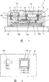
具体实施方式
图1为本发明实施形态的陶瓷微型组件1的剖面图。图2为微型组件1的陶瓷基板13的俯视图。陶瓷微型组件1有陶瓷基板13。陶瓷基板13具有在其内部构成层状的内部电极2、用于连接内部电极2之间的通路电极3、及绝缘材料即陶瓷材料14。片状电阻器、层叠陶瓷电容器、片状线圈等器件6具有本体6A和端面电极15。IC、SAW滤波器等有源器件8具有本体8A和凸点电极16。器件6的端面电极15和有源器件8的凸点电极16用焊剂7与焊盘电极4连接,器件6、8设在基板13的表面13A上。将陶瓷微型组件1装在母板40上用的背面电极5设在陶瓷基板13的下底面13B上。凹部10B形成于与器件6对向的陶瓷基板13的表面,凹部10A形成于与有源器件8对向的陶瓷基板13的表面。器件6和基板13之间充填环氧树脂等绝缘性树脂11,在有源器件8和基板13之间充填树脂9。器件6、有源器件8、和陶瓷基板13的安装器件6、有源器件8的表面被浇注树脂12覆盖。
陶瓷基板13的内部电极2及通路电极3要和陶瓷基板13同时烧结,因为最好尽可能是高电导率的材料,所以用银糊。陶瓷基板13的陶瓷材料14由于内部电极2采用Ag,故而需要约900℃才能烧结。实施形态中,陶瓷材料14由Al2O3及玻璃组成的玻璃陶瓷组成物构成。内部电极2和陶瓷材料14也可以利用上述以外的材料构成。
浇注树脂12由环氧树脂、酚醛树脂、或环氧硅树脂等绝缘树脂构成,能确保微型组件1的器件60、80的安装强度及耐冲击性。焊料7也可以是采用导电树脂的导电接合剂。
器件6和有源器件8安装在陶瓷基板13上,并电连接。器件6安装在陶瓷基板13的焊盘电极4上后,将树脂11填入元器件6和陶瓷基板13之间的包含凹部10B在内的空间10C。利用凹部10B,树脂11能容易填入器件6和陶瓷基板13之间。通过这样,由于器件6和陶瓷基板13之间无间隙产生,所以,在微型组件1安装在母板40上时,即使进行加热,焊料7也不会流出,能防止电极4间短路。尤其是器件6小的时候,由于电极4间的间隙狭窄,故凹部10B对于充填树脂11是相当有用的。
在安装有源器件8时,为了确保安装强度及安装可靠性,在器件8和基板13之间充填由环氧树脂等绝缘树脂组成的树脂9。树脂9也可由其它树脂构成。尽管器件8和基板13间的间隔狭窄,但凹部10A仍能十分容易地充填树脂9,能防止器件8和基板13之间产生空隙。由此,能获得安装强度及安装可靠性俱佳的陶瓷微型组件1。
为了使器件6和有源器件8的下部稳定充填树脂11、9,如图2所示,器件6和有源器件8的对向焊盘电极4之间的距离W1和凹部10A、10B的宽度W2为W1≥W2,最好凹部10A、10B的深度在10μm以上。通过这样,能确实地防止在将器件6装在基板13上时由于焊料的回流、或导电接合剂的流出而造成电极4间短路、或充填在有源器件8之下的树脂9的量不足,能获得器件6、8的安装强度大、高可靠性的陶瓷微型组件1。
图3~图13为表示陶瓷基板13的制造方法的剖面图。
陶瓷基板13系烧结Al2O3和玻璃粉末组成的玻璃陶瓷原料片后而得。作为玻璃粉末可以从SiO2、B2O3、Al2O3、CaCO3、SrCO3、BaCO3、La2O3、ZrO2、TiO2、MgO、PbO、ZnO、Li2CO3、Na2CO3、及K2CO3中选择适当的组份而构成。通过在Al2O3和玻璃粉末中加入聚乙烯醇缩丁醛系接合剂、增塑剂、有机溶剂并使其分散得到浆料。还有,上述组成是一个示例,也可以用除此以外其它的组成来形成浆料。
用刮片法等将所得的浆料涂布于基膜21上,并使其干燥,如图3所示,在PET膜构成的基膜21上形成所需的厚度和面积的陶瓷原料片20。基膜21也可由PET膜以外的材料构成。
然后如图4所示,用冲孔或激光加工等方法,在陶瓷原料片20上形成贯穿孔22。还择需在基膜上形成层叠用的导向孔27。
然后如图5所示,将银糊等导电糊充填入贯穿孔22,形成通路电极23。此后,如图6所示,利用利网印刷形成内部电极24。内部电极24是通过印刷以Ag为主成分的导电糊形成,但只要能和陶瓷原料片20同时烧结,则也可以用除Ag以外的导电糊。
此后如图7所示,通过使导向销27穿过导向孔27,从而使分别具有原料片20A、通路电极23、和内部电极24的多片基膜21位置对准。然后,将原料片20A放在层叠板25上。此后,通过使导向销26穿过导向孔27而对准位置,再将原料片20B放在层叠板25上已放置的原料片20A上,以后同样地将原料片20C放在原料片20B上,然后又将原料片20D放在原料片20C上。
然后形成图8示出的包括陶瓷原料片20A~20D在内的层叠体块28。层叠体块28的表层形成焊盘电极4。导向孔27形成于基膜21,但也可形成于原料片20A~20D。使陶瓷原料片20A~20D的密度均匀,为了不使陶瓷原料片20A~20D之间分层,在层叠体块28上施加压力F,使陶瓷原料片20A~20D压紧。
然后,在350~600℃下对层叠体块28脱脂,此后在850~950℃下烧结,如图9所示,得到具有用Ag构成的内部电极24的陶瓷基板13。
然后如图10所示,用激光29在陶瓷基板13的表面焊盘电极4之间的部分形成凹部30。利用激光29能在短时间内形成凹部30。
此后,用焊料将器件6的端面电极15和电极4连接后,在凹部30中填入环氧树脂、硅树脂等树脂11后,再使其固化。由此,在这道工序以后,在将其它的元器件装在基板13上时即使进行加热,仍能利用充填在凹部30的树脂11不让焊料7流向电极4之间,防止电极4间短路。
在安装有源器件8时,为确保安装强度及安装可靠性,在基板13上将凹部30形成于有源器件8的下面后将树脂9充填入凹部30使其固化。由此,树脂9能无空隙地充填入器件8和基板13之间,能得到安装强度及可靠性俱佳的陶瓷微型组件1。
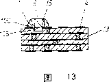
在形成焊盘电极4时,如图11所示,形成作为连续的大的焊盘电极4A,并将陶瓷基板13烧结。此后,如图12所示,用激光29在基板13上形成凹部30,同时分割焊盘电极4A,凹部30和电极4能同时形成。由此,即使在焊盘电极4极其小时,也不必过分地确保导电糊的不被擦伤、或印刷精度等,能在焊盘电极4之间高精度地形成凹部30。
然后如图13所示,安装器件6及有源器件8(未图示)后,利用环氧树脂等树脂材料将树脂11填入器件6的下面及凹部30。此后,形成浇注树脂12后,用划片等切断成规定的尺寸,得到陶瓷微型组件1。
陶瓷基板13上的电极4、4A可以和陶瓷基板13同时烧结,也可以在陶瓷基板13烧结之后再烧结。
图14至图16为说明实施形态的陶瓷微型组件的其它制造方法用的剖面图。在图4所示的陶瓷原料片上利用冲孔或激光的激光加工形成贯穿孔22时,如图14所示,在陶瓷基板13的最表层的陶瓷原料片20D上,同时在焊盘电极4之间形成凹部10A、10B的部分上形成贯穿孔22A。此后,和图5~图11一样,如图15所示,在贯穿孔22中形成通路电极23,如图16所示,形成内部电极24,再将原料片20A~20D层叠在一起后烧结。由此,层叠体块28上贯穿孔22A成为凹部10A、10B。此后,如图13所示,安装上器件6、8,形成树脂9、10和浇注树脂12得到陶瓷微型组件1。通过这样,不在陶瓷原料片20A~20D烧结后形成凹部,而能形成凹部10A、10B。
还有,也可以通过对烧结前的层叠体块28进行激光加工而形成规定凹部30。此后,利用层叠体块28的烧结、器件6及8的安装、树脂9及11和浇注树脂23的形成,得到陶瓷微型组件1。
又如图17所示,在对层叠体块28加压时,通过将金属模具41配置在焊盘电极4之间加压,而在焊盘电极4之间形成凹部30。又如图12所示,在烧结前,可利用激光对层叠体块28在焊盘电极4之间形成凹部30。还有,能在加压前后的无论前或后,利用激光形成凹部30。此后,利用层叠体块28的烧结、器件6及8的安装、树脂9及11和浇注树脂12的形成,能简便而可靠地获得具有在焊盘电极4之间形成的凹部10A、10B的陶瓷微型组件1。
Claims (19)
1.一种微型组件,其特征在于,包括
具有形成凹部、且包围所述凹部的整个外周的第一面、所述凹部的底部位于比所述第一面更内部的陶瓷基板;
将所示凹部夹在其间、并设置在所述陶瓷基板的所述第一面上的第一和第二电极;
有分别连接所述第一和第二电极的第三和第四电极并设置在所述陶瓷基板的所述凹部的上方、而且在和所述陶瓷基板之间形成包括所述凹部在内的空间的器件;及
充填入所述器件和所述陶瓷基板之间的所述空间用的树脂。
2.如权利要求1所述的微型组件,其特征在于,还包括
覆盖所述器件的浇注树脂。
3.如权利要求2所述的微型组件,其特征在于,
所述浇注树脂覆盖所述器件和所述陶瓷基板的所述第一面。
4.如权利要求1所述的微型组件,其特征在于,
所述凹部的深度在10μm以上。
5.如权利要求1所述的微型组件,其特征在于,
所述陶瓷基板还有第二面,还包括设在所述陶瓷基板的所述第二面上的第五电极。
6.一种微型组件的制造方法,其特征在于,包括
准备具有形成凹部、且包围所述凹部的整个外周的第一面、所述凹部的底部位于比所述第一面更内部的陶瓷基板的步骤;
将所述凹部夹在其间、在所述陶瓷基板的所述第一面上设置第一和第二电极的步骤;
准备具有本体及第三和第四电极的器件的步骤;
在所述陶瓷基板所示凹部的上方设置所述器件,使得在所述第一和第二电极的上方将所述第一和第二电极分别与第三和第四电极连接、并在和所述陶瓷基板之间形成包括所述凹部在内的空间的步骤;及
将树脂充填入所述器件和所述陶瓷基板之间的所述空间中的步骤。
7.如权利要求6所述的制造方法,其特征在于,还包括
设置覆盖所述器件和所述陶瓷基板的所述第一面的浇注树脂。
8.如权利要求6所述的制造方法,其特征在于,
所述凹部的深度为10μm以上。
9.如权利要求6所述的制造方法,其特征在于,
所述陶瓷基板还有第二面,还包括在所述陶瓷基板的所述第二面上设置第五电极的步骤。
10.如权利要求6所述的制造方法,其特征在于,
准备所述陶瓷基板的步骤包括
烧结具有与所述陶瓷基板的所述第一面对应的第一面的陶瓷原料片的步骤;及
在所述烧结的陶瓷原料片的所述第一面上形成所述凹部的步骤。
11.如权利要求10所述的制造方法,其特征在于,
在所述烧结的陶瓷原料片的所述第一面形成所述凹部的步骤还包括利用激光在所述烧结的陶瓷原料片的所述第一面上形成所述凹部的步骤。
12.如权利要求6所述的制造方法,其特征在于,
准备具有形成所述凹部的所述第一面的所述陶瓷基板的步骤包括在陶瓷基板上形成所述凹部的步骤,
在所述陶瓷基板的所述第一面上设置所述第一和第二电极的步骤包括
在所述陶瓷基板的所述第一面的所述凹部形成所述第一和第二电极的部分上设置第六电极的步骤;及
和在所述陶瓷基板的所述第一面上形成所述凹部的步骤同时分割所述第六电极而设置所述第一和第二的电极的步骤。
13.如权利要求6所述的制造方法,其特征在于,
准备所述陶瓷基板的步骤包括
准备具有与所述陶瓷基板的所述第一面对应的第一面和所述第一面相反一侧的第二面的第一陶瓷原料片的步骤;
在所述第一原料片的所述第一面上形成与所述陶瓷基板的所述凹部对应的规定凹部的步骤;及
烧结形成所述规定凹部的所述第一陶瓷原料片的步骤。
14.如权利要求13所述的制造方法,其特征在于,
在所述陶瓷原料片的所述第一面上形成所述规定凹部的步骤包括利用激光加工在所述第一陶瓷原料片的所述第一面上形成所述规定凹部的步骤。
15.如权利要求13所述的制造方法,其特征在于,
准备所述陶瓷基板的步骤还包括在具有形成所述规定凹部的所述第一面的所述第一陶瓷原料片的第二面上层叠第二陶瓷原料片的步骤,
烧结形成所述凹部的所述第一陶瓷原料片的步骤包括烧结层叠着所述第二陶瓷原料片的所述第一陶瓷原料片的步骤。
16.如权利要求13所述的制造方法,其特征在于,
准备所述陶瓷基板的步骤包括
将第二陶瓷原料片层叠在所述第一陶瓷原料片的所述第二面上形成层叠体块的步骤;及
对所述层叠体块加压使所述第一陶瓷原料片和所述第二陶瓷原料片压紧的步骤,
在所述第一陶瓷原料片的所述第一面形成所述规定凹部的步骤包括对所述层叠体块加压使所述第一陶瓷原料片和所述第二陶瓷原料片压紧的步骤的同时在所述第一陶瓷原料片的所述第一面形成所述规定凹部的步骤。
17.如权利要求6所述的制造方法,其特征在于,
准备所述陶瓷基板的步骤包括
准备具有与所述陶瓷基板的所述第一面对应的第一面和所述第一面相反一侧的第二面的第一陶瓷原料片的步骤;
在所述第一陶瓷原料片上形成贯穿所述第一陶瓷原料片的所述第一面和所述第二面的第一贯穿孔的步骤;
在与所述凹部对应的部分、在所述第一陶瓷原料片上形成贯穿所述第一陶瓷原料片的所述第一面和所述第二面的第二贯穿孔的步骤;
将导电糊充填入所述第一贯穿孔的步骤;
在所述第一陶瓷原料片的所述第二面上层叠第二陶瓷原料片、形成层叠体块的步骤;及
烧结所述层叠体块的步骤。
18.如权利要求16所述的制造方法,其特征在于,
在所述第一陶瓷原料片上形成所述第一贯穿孔的步骤包括利用冲孔在所述第一陶瓷原料片上形成所述第一贯穿孔的步骤,在所述第一陶瓷原料片上形成所述第二贯穿孔的步骤包括利用冲孔在所述第一陶瓷原料片上形成所述第二贯穿孔的步骤。
19.如权利要求16所述的制造方法,其特征在于,
在所述第一陶瓷原料片上形成所述第一贯穿孔的步骤包括利用激光加工在所述第一陶瓷原料片上形成所述第一贯穿孔的步骤,在所述第一陶瓷原料片上形成所述第二贯穿孔的步骤包括利用激光加工在所述第一陶瓷原料片上形成所述第二贯穿孔的步骤。
Applications Claiming Priority (2)
| Application Number | Priority Date | Filing Date | Title |
|---|---|---|---|
| JP2003337180 | 2003-09-29 | ||
| JP2003337180A JP2005108950A (ja) | 2003-09-29 | 2003-09-29 | セラミックモジュール部品およびその製造方法 |
Publications (2)
| Publication Number | Publication Date |
|---|---|
| CN1604721A CN1604721A (zh) | 2005-04-06 |
| CN100369532C true CN100369532C (zh) | 2008-02-13 |
Family
ID=34191559
Family Applications (1)
| Application Number | Title | Priority Date | Filing Date |
|---|---|---|---|
| CNB2004100831181A Expired - Fee Related CN100369532C (zh) | 2003-09-29 | 2004-09-29 | 微型组件及其制造方法 |
Country Status (5)
| Country | Link |
|---|---|
| US (1) | US7231712B2 (zh) |
| EP (1) | EP1519641B1 (zh) |
| JP (1) | JP2005108950A (zh) |
| CN (1) | CN100369532C (zh) |
| DE (1) | DE602004030081D1 (zh) |
Cited By (1)
| Publication number | Priority date | Publication date | Assignee | Title |
|---|---|---|---|---|
| CN103929880A (zh) * | 2013-01-10 | 2014-07-16 | 元太科技工业股份有限公司 | 电路基板结构及其制作方法 |
Families Citing this family (18)
| Publication number | Priority date | Publication date | Assignee | Title |
|---|---|---|---|---|
| US7202571B2 (en) | 2004-08-16 | 2007-04-10 | Delphi Technologies, Inc. | Electronic module with form in-place pedestal |
| KR100857011B1 (ko) * | 2005-03-04 | 2008-09-04 | 가부시키가이샤 무라타 세이사쿠쇼 | 세라믹 다층 기판 및 그 제조방법 |
| JP4145902B2 (ja) * | 2005-07-19 | 2008-09-03 | セイコーエプソン株式会社 | 半導体装置及びその製造方法 |
| CN101091312B (zh) * | 2005-11-02 | 2011-12-28 | 松下电器产业株式会社 | 电子部件组件 |
| JP4946565B2 (ja) * | 2007-03-27 | 2012-06-06 | 株式会社デンソー | モールドパッケージおよびその製造方法 |
| KR101011199B1 (ko) * | 2007-11-01 | 2011-01-26 | 파나소닉 주식회사 | 실장 구조체 |
| JP2011100718A (ja) * | 2009-10-05 | 2011-05-19 | Yazaki Corp | コネクタ |
| JP5711472B2 (ja) * | 2010-06-09 | 2015-04-30 | 新光電気工業株式会社 | 配線基板及びその製造方法並びに半導体装置 |
| JP5772970B2 (ja) * | 2011-10-21 | 2015-09-02 | 株式会社村田製作所 | 多層配線基板、プローブカード及び多層配線基板の製造方法 |
| WO2014156393A1 (ja) | 2013-03-27 | 2014-10-02 | 株式会社村田製作所 | 絶縁性セラミックペースト、セラミック電子部品およびその製造方法 |
| JP6418237B2 (ja) | 2014-05-08 | 2018-11-07 | 株式会社村田製作所 | 樹脂多層基板およびその製造方法 |
| US9902006B2 (en) | 2014-07-25 | 2018-02-27 | Raytheon Company | Apparatus for cleaning an electronic circuit board |
| WO2016098628A1 (ja) * | 2014-12-17 | 2016-06-23 | 株式会社 村田製作所 | 積層セラミック電子部品およびその製造方法 |
| JP6589301B2 (ja) * | 2015-03-10 | 2019-10-16 | セイコーエプソン株式会社 | 液体噴射ヘッド、及び液体噴射ヘッドの製造方法 |
| CN208159004U (zh) * | 2015-11-05 | 2018-11-27 | 株式会社村田制作所 | 部件安装基板 |
| CN105428508B (zh) | 2015-12-02 | 2018-08-24 | 开发晶照明(厦门)有限公司 | 封装基板以及led倒装封装结构 |
| TWI562410B (en) * | 2015-12-02 | 2016-12-11 | Kaistar Lighting Xiamen Co Ltd | Packaging Substrate and LED Flip Chip Packaging structure |
| EP3468312B1 (en) * | 2017-10-06 | 2023-11-29 | AT & S Austria Technologie & Systemtechnik Aktiengesellschaft | Method of manufacturing a component carrier having a three dimensionally printed wiring structure |
Citations (8)
| Publication number | Priority date | Publication date | Assignee | Title |
|---|---|---|---|---|
| US5010212A (en) * | 1988-05-31 | 1991-04-23 | Aisin Seiki K.K. | Resin coated electric circuit board device |
| JPH08181251A (ja) * | 1994-12-27 | 1996-07-12 | Sumitomo Kinzoku Electro Device:Kk | セラミック多層基板 |
| JPH10233463A (ja) * | 1997-01-27 | 1998-09-02 | Toshiba Corp | 半導体装置およびその製造方法 |
| WO1999003145A1 (de) * | 1997-07-08 | 1999-01-21 | Robert Bosch Gmbh | Verfahren zur herstellung einer klebeverbindung zwischen einem elektronischen bauelement und einem trägersubstrat |
| JPH11346056A (ja) * | 1998-06-01 | 1999-12-14 | Murata Mfg Co Ltd | キャビティ付きセラミック多層基板の製造方法及びキャビティ付きセラミック多層基板 |
| JP2001244578A (ja) * | 2000-02-29 | 2001-09-07 | Fuji Xerox Co Ltd | 積層基板 |
| US6521997B1 (en) * | 2001-12-06 | 2003-02-18 | Siliconware Precision Industries Co., Ltd. | Chip carrier for accommodating passive component |
| JP2003273156A (ja) * | 2002-03-18 | 2003-09-26 | Denso Corp | 電子装置及びその製造方法 |
Family Cites Families (8)
| Publication number | Priority date | Publication date | Assignee | Title |
|---|---|---|---|---|
| JPH03205857A (ja) | 1990-01-06 | 1991-09-09 | Fujitsu Ltd | 樹脂封止型電子部品 |
| JPH0483392A (ja) * | 1990-07-25 | 1992-03-17 | Narumi China Corp | 電子用セラミック基板の製造方法 |
| JPH04252041A (ja) | 1991-01-28 | 1992-09-08 | Nec Corp | 混成集積回路の製造方法 |
| JP3648277B2 (ja) * | 1995-01-12 | 2005-05-18 | 株式会社東芝 | 半導体装置 |
| JP3565724B2 (ja) * | 1998-10-06 | 2004-09-15 | 沖電気工業株式会社 | フリップチップ型半導体パッケージ及びその装置における樹脂注入方法 |
| JP2001244376A (ja) * | 2000-02-28 | 2001-09-07 | Hitachi Ltd | 半導体装置 |
| JP3531573B2 (ja) * | 2000-03-17 | 2004-05-31 | 株式会社村田製作所 | 積層型セラミック電子部品およびその製造方法ならびに電子装置 |
| JP3511982B2 (ja) * | 2000-06-14 | 2004-03-29 | 株式会社村田製作所 | 多層配線基板の製造方法 |
-
2003
- 2003-09-29 JP JP2003337180A patent/JP2005108950A/ja active Pending
-
2004
- 2004-09-27 EP EP04022953A patent/EP1519641B1/en not_active Expired - Fee Related
- 2004-09-27 DE DE602004030081T patent/DE602004030081D1/de active Active
- 2004-09-29 CN CNB2004100831181A patent/CN100369532C/zh not_active Expired - Fee Related
- 2004-09-29 US US10/952,476 patent/US7231712B2/en not_active Expired - Fee Related
Patent Citations (8)
| Publication number | Priority date | Publication date | Assignee | Title |
|---|---|---|---|---|
| US5010212A (en) * | 1988-05-31 | 1991-04-23 | Aisin Seiki K.K. | Resin coated electric circuit board device |
| JPH08181251A (ja) * | 1994-12-27 | 1996-07-12 | Sumitomo Kinzoku Electro Device:Kk | セラミック多層基板 |
| JPH10233463A (ja) * | 1997-01-27 | 1998-09-02 | Toshiba Corp | 半導体装置およびその製造方法 |
| WO1999003145A1 (de) * | 1997-07-08 | 1999-01-21 | Robert Bosch Gmbh | Verfahren zur herstellung einer klebeverbindung zwischen einem elektronischen bauelement und einem trägersubstrat |
| JPH11346056A (ja) * | 1998-06-01 | 1999-12-14 | Murata Mfg Co Ltd | キャビティ付きセラミック多層基板の製造方法及びキャビティ付きセラミック多層基板 |
| JP2001244578A (ja) * | 2000-02-29 | 2001-09-07 | Fuji Xerox Co Ltd | 積層基板 |
| US6521997B1 (en) * | 2001-12-06 | 2003-02-18 | Siliconware Precision Industries Co., Ltd. | Chip carrier for accommodating passive component |
| JP2003273156A (ja) * | 2002-03-18 | 2003-09-26 | Denso Corp | 電子装置及びその製造方法 |
Cited By (2)
| Publication number | Priority date | Publication date | Assignee | Title |
|---|---|---|---|---|
| CN103929880A (zh) * | 2013-01-10 | 2014-07-16 | 元太科技工业股份有限公司 | 电路基板结构及其制作方法 |
| US9791753B2 (en) | 2013-01-10 | 2017-10-17 | E Ink Holdings Inc. | Circuit substrate structure and method for manufacturing thereof |
Also Published As
| Publication number | Publication date |
|---|---|
| US20050067177A1 (en) | 2005-03-31 |
| DE602004030081D1 (de) | 2010-12-30 |
| EP1519641B1 (en) | 2010-11-17 |
| JP2005108950A (ja) | 2005-04-21 |
| EP1519641A2 (en) | 2005-03-30 |
| EP1519641A3 (en) | 2005-08-24 |
| CN1604721A (zh) | 2005-04-06 |
| US7231712B2 (en) | 2007-06-19 |
Similar Documents
| Publication | Publication Date | Title |
|---|---|---|
| CN100369532C (zh) | 微型组件及其制造方法 | |
| US9609743B2 (en) | Electronic device mounting substrate, electronic apparatus, and imaging module | |
| US6011683A (en) | Thin multilayer ceramic capacitors | |
| US10699993B2 (en) | Wiring board, electronic device, and electronic module | |
| US10985098B2 (en) | Electronic component mounting substrate, electronic device, and electronic module | |
| JP6039311B2 (ja) | 配線基板、電子装置および電子モジュール | |
| CN107615477B (zh) | 电子元件安装用基板以及电子装置 | |
| JP2007173629A (ja) | 電子部品収納用パッケージおよび電子装置 | |
| CN113169129A (zh) | 电子元件安装用基板以及电子装置 | |
| JP2004288660A (ja) | 配線基板 | |
| US10290591B2 (en) | Wiring board, electronic device, and electronic module | |
| JP3716165B2 (ja) | 圧力検出装置用パッケージおよび圧力検出装置 | |
| JP4369732B2 (ja) | 電子装置 | |
| JPH11111766A (ja) | 配線基板およびその製造方法 | |
| JP6403092B2 (ja) | セラミック基板およびそれを用いた電子部品の製造方法 | |
| JP6441696B2 (ja) | 配線基板、電子装置および電子モジュール | |
| JP2003224222A (ja) | 半導体素子収納用パッケージ | |
| JP4077690B2 (ja) | 圧力検出装置用パッケージ | |
| JP5240724B2 (ja) | 電子部品搭載用基板 | |
| JP2003110247A (ja) | 多層回路基板及びその製造方法 | |
| JP2004235206A (ja) | セラミック多層回路基板 | |
| JP2003243553A (ja) | 配線基板 | |
| JP2003332479A (ja) | 半導体素子収納用パッケージおよびその製造方法 | |
| JP2003142633A (ja) | 配線基板の製造方法 | |
| JP2002131163A (ja) | 圧力検出装置用パッケージ |
Legal Events
| Date | Code | Title | Description |
|---|---|---|---|
| C06 | Publication | ||
| PB01 | Publication | ||
| C10 | Entry into substantive examination | ||
| SE01 | Entry into force of request for substantive examination | ||
| C14 | Grant of patent or utility model | ||
| GR01 | Patent grant | ||
| C17 | Cessation of patent right | ||
| CF01 | Termination of patent right due to non-payment of annual fee |
Granted publication date: 20080213 Termination date: 20091029 |