EP1511094A2 - Licht emittierendes Bauelement und Verfahren zu seiner Herstellung - Google Patents
Licht emittierendes Bauelement und Verfahren zu seiner Herstellung Download PDFInfo
- Publication number
- EP1511094A2 EP1511094A2 EP04018867A EP04018867A EP1511094A2 EP 1511094 A2 EP1511094 A2 EP 1511094A2 EP 04018867 A EP04018867 A EP 04018867A EP 04018867 A EP04018867 A EP 04018867A EP 1511094 A2 EP1511094 A2 EP 1511094A2
- Authority
- EP
- European Patent Office
- Prior art keywords
- layer
- light
- layers
- emitting component
- doped
- Prior art date
- Legal status (The legal status is an assumption and is not a legal conclusion. Google has not performed a legal analysis and makes no representation as to the accuracy of the status listed.)
- Granted
Links
Images

Classifications
-
- H—ELECTRICITY
- H10—SEMICONDUCTOR DEVICES; ELECTRIC SOLID-STATE DEVICES NOT OTHERWISE PROVIDED FOR
- H10K—ORGANIC ELECTRIC SOLID-STATE DEVICES
- H10K50/00—Organic light-emitting devices
- H10K50/10—OLEDs or polymer light-emitting diodes [PLED]
- H10K50/14—Carrier transporting layers
-
- H—ELECTRICITY
- H10—SEMICONDUCTOR DEVICES; ELECTRIC SOLID-STATE DEVICES NOT OTHERWISE PROVIDED FOR
- H10K—ORGANIC ELECTRIC SOLID-STATE DEVICES
- H10K50/00—Organic light-emitting devices
- H10K50/10—OLEDs or polymer light-emitting diodes [PLED]
- H10K50/11—OLEDs or polymer light-emitting diodes [PLED] characterised by the electroluminescent [EL] layers
-
- H—ELECTRICITY
- H10—SEMICONDUCTOR DEVICES; ELECTRIC SOLID-STATE DEVICES NOT OTHERWISE PROVIDED FOR
- H10K—ORGANIC ELECTRIC SOLID-STATE DEVICES
- H10K50/00—Organic light-emitting devices
- H10K50/10—OLEDs or polymer light-emitting diodes [PLED]
- H10K50/14—Carrier transporting layers
- H10K50/15—Hole transporting layers
- H10K50/155—Hole transporting layers comprising dopants
-
- H—ELECTRICITY
- H10—SEMICONDUCTOR DEVICES; ELECTRIC SOLID-STATE DEVICES NOT OTHERWISE PROVIDED FOR
- H10K—ORGANIC ELECTRIC SOLID-STATE DEVICES
- H10K50/00—Organic light-emitting devices
- H10K50/10—OLEDs or polymer light-emitting diodes [PLED]
- H10K50/14—Carrier transporting layers
- H10K50/16—Electron transporting layers
- H10K50/165—Electron transporting layers comprising dopants
-
- H—ELECTRICITY
- H10—SEMICONDUCTOR DEVICES; ELECTRIC SOLID-STATE DEVICES NOT OTHERWISE PROVIDED FOR
- H10K—ORGANIC ELECTRIC SOLID-STATE DEVICES
- H10K50/00—Organic light-emitting devices
- H10K50/10—OLEDs or polymer light-emitting diodes [PLED]
- H10K50/17—Carrier injection layers
- H10K50/171—Electron injection layers
-
- H—ELECTRICITY
- H10—SEMICONDUCTOR DEVICES; ELECTRIC SOLID-STATE DEVICES NOT OTHERWISE PROVIDED FOR
- H10K—ORGANIC ELECTRIC SOLID-STATE DEVICES
- H10K71/00—Manufacture or treatment specially adapted for the organic devices covered by this subclass
- H10K71/30—Doping active layers, e.g. electron transporting layers
-
- H—ELECTRICITY
- H10—SEMICONDUCTOR DEVICES; ELECTRIC SOLID-STATE DEVICES NOT OTHERWISE PROVIDED FOR
- H10K—ORGANIC ELECTRIC SOLID-STATE DEVICES
- H10K85/00—Organic materials used in the body or electrodes of devices covered by this subclass
- H10K85/10—Organic polymers or oligomers
- H10K85/111—Organic polymers or oligomers comprising aromatic, heteroaromatic, or aryl chains, e.g. polyaniline, polyphenylene or polyphenylene vinylene
- H10K85/113—Heteroaromatic compounds comprising sulfur or selene, e.g. polythiophene
- H10K85/1135—Polyethylene dioxythiophene [PEDOT]; Derivatives thereof
-
- H—ELECTRICITY
- H10—SEMICONDUCTOR DEVICES; ELECTRIC SOLID-STATE DEVICES NOT OTHERWISE PROVIDED FOR
- H10K—ORGANIC ELECTRIC SOLID-STATE DEVICES
- H10K85/00—Organic materials used in the body or electrodes of devices covered by this subclass
- H10K85/30—Coordination compounds
-
- H—ELECTRICITY
- H10—SEMICONDUCTOR DEVICES; ELECTRIC SOLID-STATE DEVICES NOT OTHERWISE PROVIDED FOR
- H10K—ORGANIC ELECTRIC SOLID-STATE DEVICES
- H10K85/00—Organic materials used in the body or electrodes of devices covered by this subclass
- H10K85/60—Organic compounds having low molecular weight
- H10K85/611—Charge transfer complexes
-
- H—ELECTRICITY
- H10—SEMICONDUCTOR DEVICES; ELECTRIC SOLID-STATE DEVICES NOT OTHERWISE PROVIDED FOR
- H10K—ORGANIC ELECTRIC SOLID-STATE DEVICES
- H10K85/00—Organic materials used in the body or electrodes of devices covered by this subclass
- H10K85/60—Organic compounds having low molecular weight
- H10K85/631—Amine compounds having at least two aryl rest on at least one amine-nitrogen atom, e.g. triphenylamine
Definitions
- the invention relates to a light-emitting component with organic layers, in particular an organic light-emitting diode, consisting of several layers between a ground contact on a substrate and a cover contact, with as a polymer layer, which consists of polymer, formed layers and with layers formed as a molecular layer, which are made in a vacuum consist of applied small molecules.
- organic layers in particular an organic light-emitting diode, consisting of several layers between a ground contact on a substrate and a cover contact, with as a polymer layer, which consists of polymer, formed layers and with layers formed as a molecular layer, which are made in a vacuum consist of applied small molecules.
- the invention also relates to processes for the preparation of a Light emitting device, in which a substrate Basic contact, then several layers and finally one Cover contact is applied
- Organic light-emitting diodes are lower since the demonstration Working voltages of Tang et al. 1987 [C.W. Tang et al., Appl. Phys. Lett. 51 (12), 913 (1987)] are promising candidates for the realization of large-scale displays and other applications, such as. Lighting elements. They consist of an order thin (typically 1nm to 1 ⁇ m) layers of organic Materials which preferably in vacuum in the form of smaller Molecules are evaporated, creating so-called OLED be spin coated, printed or in solution be applied to other suitable form (polymers), whereby so-called PLED are generated.
- OLED organic light-emitting diodes
- the polymeric layers i. the hole transport or hole injection layer and the active polymer are made from a liquid Solution (in water or in solvents).
- the contacts typically by vacuum processes.
- the disadvantage is, among other things, that does not make sense more than two different polymeric layers are applied can, since the solvents of the polymers are chosen so need that they do not affect each other, that is do not attack the material of the pad.
- Organic light emitting diodes in the form of OLEDs are made in vacuum built up small evaporated molecules. Are the molecules which are to form the layers of the OLED, small enough, so They can usually be decomposed by a thermal Process be applied. For this, the molecules are in a vacuum (because of the large free path) evaporated.
- the transport layers can be mixed by coevaporation organic or inorganic dopants, which acceptors (for Hole doping) or donors (for electron doping), be doped.
- the dopants must be at the beginning of the evaporation process not in their final form, as long as the alternatively used precursor material in the evaporation process (which may also be modified, for example by Use of electron beams) forms the dopant.
- the production the mixed layers are typically through Mixed (co-) evaporation.
- Advantages of this structure are the separate optimizability of the properties of the individual layers, the adjustable large distance between the emitter layer and the contacts, the very good injection of the charge carriers into the organic layers and the small thickness of the layers which are not well conductive (4; 5; 6).
- Very low operating voltages ⁇ 2.6 V for 100 cd / m 2 luminance
- this structure can also be easily inverted and realize top-emitting or completely transparent OLEDs, as described in DE 102 15 210.1.
- the disadvantage of this structure is that a lateral Structuring the OLED structure to build different colored Pixels in a display can only be done via shadow masks.
- This process has limitations in terms of the smallest achievable Pixel sizes ( ⁇ 50 ⁇ m subpixels).
- the shadow mask process is a relatively expensive process in a production.
- one can use the ink-jet process for small molecules do not use because of their insolubility.
- This object is achieved on the arrangement side by arranging at least one polymer layer and two molecular layers, wherein, when the cover contact is a cathode, the layer closest to the cover contact is formed as an electron transporting molecule layer and doped by an organic or inorganic donor, wherein the n-type dopant comprises an organic main substance and a donor-like dopant and the molecular mass of the dopant is greater than 200g / mol, or if the cover contact is an anode, the layer closest to the cover contact is formed as a p-type hole transporting molecular layer and through an organic or inorganic acceptor is doped, wherein the dopant comprises an organic main substance and an acceptor-like dopant and the molecular mass of the dopant is greater than 200 g / mol.
- a substantially higher flexibility can be achieved in the layer composite, while the simultaneous presence of polymer layers serves the easier structuring without the special use of shadow masks.
- the Dotand.soll consist of an organic, inorganic or metal-organic molecule having a molar mass of greater than 200g / mol, preferably greater than 400g / mol. It is important that the dopant active in the layer has this molar mass.
- Cs 2 CO 3 cesium carbonate, molar mass about 324 g / mol
- Cs 2 CO 3 is a comparatively stable compound which is no longer able to transfer one or more electrons to another molecule (the matrix material).
- the two molecular deposited layers are the undoped ones Interlayer (reference numeral 5 in the below-described Embodiment) and the doped transport layer.
- the energetic barrier of charge carrier injection from the doped transport layer into the polymer emitter layer for common emitter polymers such as poly-phenylenevinylene, PPV, (in the case of the conventionally known layer structure with polymer hole transport layer on a substrate the Barrier to injection of electrons) is too large, one must undoped interlayer be inserted, which is essential thinner than the doped transport layer and its LUMO Energy level (LUMO: lowest unoccupied molecular orbital) in the case of the hole transport layer, however, the HOMO energy level (HOMO: highest occupied molecular orbital) between the doped transport layer and the emission polymer layer must lie.
- LUMO lowest unoccupied molecular orbital
- the object is achieved in that at least one of the layers applied as a polymer layer and at least one of the layers is vapor-deposited as a molecular layer, wherein the molecular layer is doped.
- the doping of the molecule layer takes place in a vacuum of two separately controlled sources as one Mixed evaporation.
- the order of the polymer layers can be done with simple means very precise. This structuring then serves at the same time the structuring of the later light-emitting Component without elaborate structuring steps or -ffen are required.
- the application of molecular layers on the other hand, it avoids that as a result of the presence of usually only two disjoint solvents the Modification of polymer layers is very limited and increased the possibility of building different layer combinations.
- a transparent Ground contact 2 applied as an anode.
- a first polymer layer as a polymeric hole transport layer 3 and a second polymer layer as a polymeric Emitter layer 4 deposited.
- This layer composite of first and second polymer layer consists of PEDOT: PSS (Baytron-P) by H. C. Starck, Germany.
- a first molecule layer vapor-deposited as an intermediate layer 5 which consists of a Layer of 10nm BPhen (Batophenanthrolin) exists.
- Cs has a standard redox potential of -2.922V and an ionization energy of 3.88 eV. The ionization energy of the dopant is less than 4.1 eV.
- Tungsten paddlewheel has an ionization potential of about 3.75 eV.
- the structure of the simple negative hpp anion is:
- the doped layer in the above example BPhen: Cs must have a conductivity in the range 1E-7 S / cm to 1E-3S / cm, preferably in one Range from 1E-6S / cm to 5E-5S / cm.
- the conductivity the undoped intermediate layer in the above example BPhen must be in range from about 1E-10S / cm to 5E-8S / cm.
- the conductivity the undoped layer is thus at least halfway Order of magnitude worse than that of the doped layer.
- the preferred thickness ranges of the doped layer are between 40 nm and 500 nm, preferably 50 nm to 300 nm, the undoped Intermediate layer between 2 nm and 30 nm, preferred between 5 nm and 15 nm.
- the undoped layer must because of their low conductivity much thinner than the doped Be layer.
- layer thickness and Conductivity applies mutatis mutandis to the p-doping of the hole transport layer according to the embodiment below Second
- This embodiment can be modified by using polymeric hole transport layer 3 and as a polymeric emitter layer 4 a single layer can occur, both functions takes over, therefore only one polymer layer available can be.
- the base contact 2 can also be nontransparent be formed (e.g., gold, aluminum) and then the cover contact 7 as the cathode transparent, e.g. through an in a sputtered ITO layer. Because of the doping the layer 6 is an electron injection of ITO in Layer 6 still possible. Furthermore, the dopant concentration in the case of organic dopants between 1: 1000 and 1:20 and in the case of inorganic dopants between 1: 1000 and 3: 1 lie.
- the organic according to the invention consists Light-emitting diode of both polymer and molecular layers and may therefore meaningfully be referred to as a POLED or hybrid OLED become.
- FIG. she shows an electrically inverse to Fig. 1 structure.
- a base contact 2 is applied as a cathode.
- a non-transparent cathode calcium, barium or aluminum
- ITO transparent his
- a first polymer layer as polymeric electron transport layer 8
- a second polymer layer deposited as a polymeric emitter layer 4.
- a first molecule layer as the intermediate layer 9 evaporated, which consists of a layer of 10nm TPD (tri-phenyldiamine) can exist.
- a second molecular layer in the form of a hole transport and injection layer 10 from e.g.
- the organic light-emitting diode according to FIG. 2 is provided with a Anode as cover contact 7 of e.g. transparent ITO.
Landscapes
- Physics & Mathematics (AREA)
- Optics & Photonics (AREA)
- Engineering & Computer Science (AREA)
- Chemical & Material Sciences (AREA)
- Materials Engineering (AREA)
- Manufacturing & Machinery (AREA)
- Inorganic Chemistry (AREA)
- Spectroscopy & Molecular Physics (AREA)
- Electroluminescent Light Sources (AREA)
Abstract
Description
- Fig. 1
- einen ersten Schichtaufbau einer erfindungsgemäßen organischen Leuchtdiode,
- Fig. 2
- einen zweiten, zur Fig. 1 elektrisch inversen Schichtaufbau einer erfindungsgemäßen organischen Leuchtdiode.
- 1
- Substrat
- 2
- Grundkontakt
- 3
- polymere Löchertransportschicht
- 4
- polymere Emitterschicht
- 5
- Zwischenschicht (Molekülschicht)
- 6
- dotierte Elektronentransport- und Injektionsschicht (Molekülschicht)
- 7
- Deckkontakt
- 8
- polymere Elektronentransportschicht
- 9
- Zwischenschicht (Molekülschicht)
- 10
- dotierte Löchertransport- und Injektionsschicht (Molekülschicht)
Claims (31)
- Licht emittierendes Bauelement mit organischen Schichten, bestehend aus mehreren Schichten zwischen einem Grundkontakt auf einem Substrat und einem Deckkontakt, mit als Polymerschicht, die aus Polymer besteht, ausgebildeten Schichten und mit als Molekülschicht ausgebildeten Schichten, die aus im Vakuum aufgebrachten kleinen Molekülen bestehen, dadurch gekennzeichnet, dass wenigstens eine Polymerschicht (3; 4) und zwei Molekülschichten (5; 6) angeordnet sind, wobei,wenn der Deckkontakt (7) eine Kathode ist, die dem Deckkontakt (7) nächstliegende Schicht als eine Elektronen transportierende Molekülschicht ausgebildet ist und durch einen organischen oder anorganischen Donator dotiert ist, wobei der n-artige Dotand eine organische Hauptsubstanz und eine donatorartige Dotiersubstanz umfasst und die molekulare Masse des Dotanden größer 200g/mol ist,
oder,wenn der Deckkontakt (7) eine Anode ist, die dem Deckkontakt (7) nächstliegende Schicht als eine p-dotierte Löcher transportierende Molekülschicht ausgebildet ist und durch einen organischen oder anorganischen Akzeptor dotiert ist, wobei der Dotand eine organische Hauptsubstanz und eine akzeptorartige Dotiersubstanz umfasst und die molekulare Masse des Dotanden größer 200 g/mol ist. - Licht emittierendes Bauelement nach Anspruch 1, dadurch gekennzeichnet, dass eine Polymerschicht angeordnet ist, die gleichzeitig eine Emitter- und eine Transportschicht bildet.
- Licht emittierendes Bauelement nach Anspruch 1 oder 2, dadurch gekennzeichnet, dass mehr als zwei Polymerschichten (3; 4) angeordnet sind.
- Licht emittierendes Bauelement nach einem der Ansprüche 1 bis 3, dadurch gekennzeichnet, dass nur eine Molekülschicht angeordnet ist, die dotiert ist.
- Licht emittierendes Bauelement nach einem der Ansprüche 1 bis 3, dadurch gekennzeichnet, dass das matrixmaterial der dotierten Schicht (9) gleich dem Matrixmaterial der Zwischenschicht (5) ist.
- Licht emittierendes Bauelement nach einem der Ansprüche 1 bis 5, dadurch gekennzeichnet, dass auf dem Grundkontakt (2) eine oder mehrere dotierte oder undotierte Molekülschichten und auf deren dem Grundkontakt (2) abgewandten Seite eine oder mehrere Polymerschichten angeordnet sind.
- Licht emittierendes Bauelement nach einem der Ansprüche 1 oder 2, dadurch gekennzeichnet, dass eine Polymerschicht angeordnet ist, an der sowohl auf ihrer dem Grundkontakt (2) zugewandten Seite als auch auf ihrer dem Deckkontakt (7) zugewandten Seite je eine Molekülschicht angrenzt.
- Licht emittierendes Bauelement nach einem der Ansprüche 1 bis 7, dadurch gekennzeichnet, dass Kontakte (2; 7) transparent ausgebildet sind.
- Licht emittierendes Bauelement nach einem der Ansprüche 1 bis 8, dadurch gekennzeichnet, dass es aus einer Mehrfachanordnung gleicher Licht emittierender Bauelemente besteht, die miteinander mittels einer Verbindungssicht elektrisch miteinander verbunden sind.
- Licht emittierendes Bauelement nach Anspruch 9, dadurch gekennzeichnet, dass die Verbindungsschicht mit einem Kontakt versehen ist und über diesen ansteuerbar ist.
- Licht emittierendes Bauelement nach Anspruch 9 oder 10, dadurch gekennzeichnet, dass die Verbindungsschicht und/oder der Kontakt transparent ausgeführt sind.
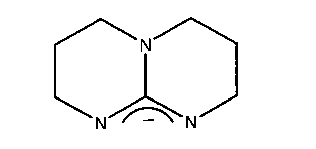
- Licht emittierendes Bauelement nach einem der Ansprüche 1 bis 11, dadurch gekennzeichnet, dass der Donator-Dotand in der Elektronentransportschicht Wolfram-Paddlewheel [W2(hpp)4] mit hpp = 1,3,4,6,7,8-Hexahydro-2H-pyrimido-[1,2-a]-pyrimidin ist.
- Licht emittierendes Bauelement nach einem der Ansprüche 1 bis 12, dadurch gekennzeichnet, dass die dotierte Schicht eine Leitfähigkeit im einem Bereich von 1E-7 S/cm bis 1E-3S/cm aufweist.
- Licht emittierendes Bauelement nach einem der Ansprüche 1 bis 13, dadurch gekennzeichnet, dass die dotierte Schicht eine Leitfähigkeit im einem Bereich von 1E-6S/cm bis 5E-5S/cm aufweist.
- Licht emittierendes Bauelement nach einem der Ansprüche 1 bis 14, dadurch gekennzeichnet, dass die Leitfähigkeit der undotierten Zwischenschicht wenigstens eine halbe Größenordnung geringer als die Leitfähigkeit der dotierten Schicht ist.
- Licht emittierendes Bauelement nach einem der Ansprüche 1 bis 15, dadurch gekennzeichnet, dass die dotierte Schicht eine Dicke in einem Bereich von 40 nm bis 500 nm aufweist.
- Licht emittierendes Bauelement nach einem der Ansprüche 1 bis 16, dadurch gekennzeichnet, dass die dotierte Schicht eine Dicke in einem Bereich von 50 nm bis 300 nm aufweist.
- Licht emittierendes Bauelement nach einem der Ansprüche 1 bis 17, dadurch gekennzeichnet, dass die undotierte Zwischenschicht eine Dicke in einem Bereich von 2 nm und 30 nm aufweist.
- Licht emittierendes Bauelement nach einem der Ansprüche 1 bis 18, dadurch gekennzeichnet, dass die undotierte Zwischenschicht eine Dicke in einem Bereich von 5 nm und 15 nm aufweist.
- Licht emittierendes Bauelement nach einem der Ansprüche 1 bis 19, dadurch gekennzeichnet, dass die undotierte Schicht dünner als die dotierte Schicht ausgebildet ist.
- Licht emittierendes Bauelement nach einem der Ansprüche 1 bis 20, dadurch gekennzeichnet, dass der Donator-Dotand ein Ionisationspotential von kleiner als 4,1 eV aufweist.
- Licht emittierendes Bauelement nach einem der Ansprüche 1 bis 21, dadurch gekennzeichnet, dass die Dotanden-Konzentration im Falle organischer Dotanden zwischen 1:1000 und 1:20 und im Falle anorganischer Dotanden zwischen 1:1000 und 3:1 beträgt.
- Verfahren zur Herstellung eines Licht emittierenden Bauelementes nach einem der Ansprüche 1 bis 22, bei dem auf ein Substrat ein Grundkontakt, danach mehrere Schichten und schließlich ein Deckkontakt aufgebracht wird, dadurch gekennzeichnet, dass mindestens eine der Schichten als Polymerschicht aufgetragen und mindestens eine der Schichten als Molekülschicht aufgedampft wird, wobei die Molekülschicht dotiert wird.
- Verfahren nach Anspruch 23, dass die Dotierung der Molekülschicht in einem Vakuum aus zwei separat geregelten Quellen als eine Mischverdampfung erfolgt.
- Verfahren nach Anspruch 23 oder 24, dadurch gekennzeichnet, dass die Dotanden erst im Vakuum aus einem Precursor erzeugt wird, wobei ein als Precursor wirkendes Ausgangsmaterial verdampft wird, welches während des Verdampfungsprozesses den Dotanden bildet.
- Verfahren nach Anspruch 23 bis 25, dadurch gekennzeichnet, dass die Dotanden-Konzentration im Falle organischer Dotanden zwischen 1:1000 und 1:20 und im Falle anorganischer Dotanden zwischen 1:1000 und 3:1 liegt.
- Verfahren nach einem der Ansprüche 23 bis 26, dadurch gekennzeichnet, dass der Auftrag der Polymerschicht nach dem Prinzip eines Tintenstrahldruckes (Ink-Jet Printing) erfolgt.
- Verfahren nach Anspruch 27, dadurch gekennzeichnet, dass die Emissionsschicht (4) zur Herstellung einer Multicolor-OLED lateral durch Ink-Jet Printing derart strukturiert wird, dass rote, grüne und blaue Pixel nebeneinander entstehen.
- Verfahren nach einem der Ansprüche 23 bis 28, dadurch gekennzeichnet, dass die Dicke aller Schichten im Bereich 0.1 nm bis 1 µm liegt.
- Verfahren nach einem der Ansprüche 23 bis 29, dadurch gekennzeichnet, dass zumindest eine der Polymerschichten durch Aufbringen einer gemischten Schicht aus einer Lösung oder durch Hintereinanderaufbringen der Materialien mit anschließender Diffusion der Dotanden in die Polymerschicht hergestellt und dotiert wird.
- Verfahren nach einem der Ansprüche 23 bis 30, dadurch gekennzeichnet, dass in der Elektronentransportschicht als Donator-Dotand Wolfram-Paddlewheel [W2(hpp)4] mit hpp = 1,3,4,6,7,8-Hexahydro-2H-pyrimido-[1,2-a]-pyrimidin verwendet wird.
Applications Claiming Priority (2)
| Application Number | Priority Date | Filing Date | Title |
|---|---|---|---|
| DE10339772 | 2003-08-27 | ||
| DE10339772A DE10339772B4 (de) | 2003-08-27 | 2003-08-27 | Licht emittierendes Bauelement und Verfahren zu seiner Herstellung |
Publications (3)
| Publication Number | Publication Date |
|---|---|
| EP1511094A2 true EP1511094A2 (de) | 2005-03-02 |
| EP1511094A3 EP1511094A3 (de) | 2005-07-27 |
| EP1511094B1 EP1511094B1 (de) | 2017-02-22 |
Family
ID=34089248
Family Applications (1)
| Application Number | Title | Priority Date | Filing Date |
|---|---|---|---|
| EP04018867.4A Expired - Lifetime EP1511094B1 (de) | 2003-08-27 | 2004-08-10 | Licht emittierendes Bauelement und Verfahren zu seiner Herstellung |
Country Status (7)
| Country | Link |
|---|---|
| US (3) | US7355197B2 (de) |
| EP (1) | EP1511094B1 (de) |
| JP (1) | JP5184736B2 (de) |
| KR (1) | KR100685108B1 (de) |
| CN (1) | CN100559627C (de) |
| DE (1) | DE10339772B4 (de) |
| TW (1) | TWI264841B (de) |
Cited By (7)
| Publication number | Priority date | Publication date | Assignee | Title |
|---|---|---|---|---|
| EP1713136A1 (de) * | 2005-04-13 | 2006-10-18 | Novaled AG | Anordnung für eine organische Leuchtdiode vom pin-Typ und Verfahren zum Herstellen |
| KR100685108B1 (ko) * | 2003-08-27 | 2007-02-22 | 노발레드 아게 | 발광 소자 및 그의 제조 방법 |
| WO2007024007A1 (en) * | 2005-08-26 | 2007-03-01 | Showa Denko K.K. | Organic electro-luminescence element, production method and use thereof |
| EP1786050A1 (de) * | 2005-11-10 | 2007-05-16 | Novaled AG | Dotiertes organisches Halbleitermaterial |
| WO2007096537A3 (fr) * | 2006-02-27 | 2007-10-11 | Commissariat Energie Atomique | Diode organique a couche d'injection et de transport de trous en polymere conducteur. |
| EP1848049A1 (de) | 2006-04-19 | 2007-10-24 | Novaled AG | Lichtemittierendes Bauelement |
| EP2330654A1 (de) * | 2009-12-04 | 2011-06-08 | Samsung Mobile Display Co., Ltd. | Organische lichtemittierende Diodenvorrichtung |
Families Citing this family (92)
| Publication number | Priority date | Publication date | Assignee | Title |
|---|---|---|---|---|
| US20100026176A1 (en) | 2002-03-28 | 2010-02-04 | Jan Blochwitz-Nomith | Transparent, Thermally Stable Light-Emitting Component Having Organic Layers |
| AU2003292826A1 (en) * | 2003-12-25 | 2005-07-21 | Fujitsu Limited | Organic el element, organic el display, process for fabricating organic el element, and system for fabricating organic el element |
| US7540978B2 (en) * | 2004-08-05 | 2009-06-02 | Novaled Ag | Use of an organic matrix material for producing an organic semiconductor material, organic semiconductor material and electronic component |
| WO2006015567A1 (de) | 2004-08-13 | 2006-02-16 | Novaled Ag | Schichtanordnung für ein lichtemittierendes bauelement |
| DE602004006275T2 (de) * | 2004-10-07 | 2007-12-20 | Novaled Ag | Verfahren zur Dotierung von einem Halbleitermaterial mit Cäsium |
| FR2878652A1 (fr) * | 2004-11-29 | 2006-06-02 | Thomson Licensing Sa | Diode organique electroluminescente a couches dopees |
| KR101267040B1 (ko) * | 2004-12-06 | 2013-05-23 | 가부시키가이샤 한도오따이 에네루기 켄큐쇼 | 복합재료를 사용한 발광소자 및 발광장치, 및 발광소자의 제조방법 |
| DE502005002342D1 (de) * | 2005-03-15 | 2008-02-07 | Novaled Ag | Lichtemittierendes Bauelement |
| US8487527B2 (en) | 2005-05-04 | 2013-07-16 | Lg Display Co., Ltd. | Organic light emitting devices |
| US7777407B2 (en) | 2005-05-04 | 2010-08-17 | Lg Display Co., Ltd. | Organic light emitting devices comprising a doped triazine electron transport layer |
| US7811679B2 (en) | 2005-05-20 | 2010-10-12 | Lg Display Co., Ltd. | Display devices with light absorbing metal nanoparticle layers |
| US7750561B2 (en) | 2005-05-20 | 2010-07-06 | Lg Display Co., Ltd. | Stacked OLED structure |
| US7943244B2 (en) | 2005-05-20 | 2011-05-17 | Lg Display Co., Ltd. | Display device with metal-organic mixed layer anodes |
| US7728517B2 (en) | 2005-05-20 | 2010-06-01 | Lg Display Co., Ltd. | Intermediate electrodes for stacked OLEDs |
| US7795806B2 (en) | 2005-05-20 | 2010-09-14 | Lg Display Co., Ltd. | Reduced reflectance display devices containing a thin-layer metal-organic mixed layer (MOML) |
| DE502005009415D1 (de) * | 2005-05-27 | 2010-05-27 | Novaled Ag | Transparente organische Leuchtdiode |
| EP1729346A1 (de) * | 2005-06-01 | 2006-12-06 | Novaled AG | Lichtemittierendes Bauteil mit einer Elektrodenanordnung |
| EP1739765A1 (de) * | 2005-07-01 | 2007-01-03 | Novaled AG | Organische Leuchtdiode und Anordnung mit mehreren organischen Leuchtdioden |
| TWI321968B (en) | 2005-07-15 | 2010-03-11 | Lg Chemical Ltd | Organic light meitting device and method for manufacturing the same |
| US7635858B2 (en) * | 2005-08-10 | 2009-12-22 | Au Optronics Corporation | Organic light-emitting device with improved layer conductivity distribution |
| DE502005004675D1 (de) * | 2005-12-21 | 2008-08-21 | Novaled Ag | Organisches Bauelement |
| US7919010B2 (en) * | 2005-12-22 | 2011-04-05 | Novaled Ag | Doped organic semiconductor material |
| EP1804308B1 (de) * | 2005-12-23 | 2012-04-04 | Novaled AG | Organische lichtemittierende Vorrichtung mit mehreren aufeinander gestapelten organischen elektrolumineszenten Einheiten |
| DE602006001930D1 (de) * | 2005-12-23 | 2008-09-04 | Novaled Ag | tur von organischen Schichten |
| EP1808909A1 (de) | 2006-01-11 | 2007-07-18 | Novaled AG | Elekrolumineszente Lichtemissionseinrichtung |
| WO2007095061A2 (en) * | 2006-02-09 | 2007-08-23 | Qd Vision, Inc. | Device including semiconductor nanocrystals and a layer including a doped organic material and methods |
| EP1994580B1 (de) * | 2006-02-28 | 2012-05-02 | Commissariat à l'Énergie Atomique et aux Énergies Alternatives | Elektronische komponente mit p-dotiertem organischem halbleiter |
| JP5064482B2 (ja) * | 2006-03-14 | 2012-10-31 | エルジー・ケム・リミテッド | 高効率の有機発光素子およびその製造方法 |
| JP5683104B2 (ja) * | 2006-03-21 | 2015-03-11 | ノヴァレッド・アクチエンゲゼルシャフト | ドープされた有機半導体材料の製造方法及びそのために用いられる配合物 |
| DE502006000749D1 (de) * | 2006-03-21 | 2008-06-19 | Novaled Ag | Heterocyclisches Radikal oder Diradikal, deren Dimere, Oligomere, Polymere, Dispiroverbindungen und Polycyclen, deren Verwendung, organisches halbleitendes Material sowie elektronisches Bauelement |
| EP1837927A1 (de) * | 2006-03-22 | 2007-09-26 | Novaled AG | Verwendung von heterocyclischen Radikalen zur Dotierung von organischen Halbleitern |
| US20090128024A1 (en) | 2006-04-20 | 2009-05-21 | Kenichi Fukuoka | Organic light-emitting device |
| KR101384046B1 (ko) | 2006-05-11 | 2014-04-09 | 이데미쓰 고산 가부시키가이샤 | 유기 전계발광 소자 |
| JP5097700B2 (ja) | 2006-05-11 | 2012-12-12 | 出光興産株式会社 | 有機エレクトロルミネッセンス素子 |
| JPWO2008015949A1 (ja) | 2006-08-04 | 2009-12-24 | 出光興産株式会社 | 有機エレクトロルミネッセンス素子 |
| DE102007012794B3 (de) * | 2007-03-16 | 2008-06-19 | Novaled Ag | Pyrido[3,2-h]chinazoline und/oder deren 5,6-Dihydroderivate, deren Herstellungsverfahren und diese enthaltendes dotiertes organisches Halbleitermaterial |
| DE102007019260B4 (de) * | 2007-04-17 | 2020-01-16 | Novaled Gmbh | Nichtflüchtiges organisches Speicherelement |
| DE102007018456B4 (de) * | 2007-04-19 | 2022-02-24 | Novaled Gmbh | Verwendung von Hauptgruppenelementhalogeniden und/oder -pseudohalogeniden, organisches halbleitendes Matrixmaterial, elektronische und optoelektronische Bauelemente |
| EP3076451B1 (de) | 2007-04-30 | 2019-03-06 | Novaled GmbH | Oxokohlenstoff, pseudooxokohlenstoff- und radialenverbindungen sowie deren verwendung |
| EP1990847B1 (de) * | 2007-05-10 | 2018-06-20 | Novaled GmbH | Verwendung von chinoiden Bisimidazolen und deren Derivaten als Dotand zur Dotierung eines organischen halbleitenden Matrixmaterials |
| DE102007031220B4 (de) | 2007-07-04 | 2022-04-28 | Novaled Gmbh | Chinoide Verbindungen und deren Verwendung in halbleitenden Matrixmaterialien, elektronischen und optoelektronischen Bauelementen |
| JP2009076865A (ja) | 2007-08-29 | 2009-04-09 | Fujifilm Corp | 有機電界発光素子 |
| KR101548382B1 (ko) | 2007-09-14 | 2015-08-28 | 유디씨 아일랜드 리미티드 | 유기 전계 발광 소자 |
| JP5489446B2 (ja) | 2007-11-15 | 2014-05-14 | 富士フイルム株式会社 | 薄膜電界効果型トランジスタおよびそれを用いた表示装置 |
| JP5489445B2 (ja) | 2007-11-15 | 2014-05-14 | 富士フイルム株式会社 | 薄膜電界効果型トランジスタおよびそれを用いた表示装置 |
| DE102008024517A1 (de) | 2007-12-27 | 2009-07-02 | Osram Opto Semiconductors Gmbh | Strahlungsemittierender Körper und Verfahren zur Herstellung eines strahlungsemittierenden Körpers |
| JP5243972B2 (ja) | 2008-02-28 | 2013-07-24 | ユー・ディー・シー アイルランド リミテッド | 有機電界発光素子 |
| JP4555358B2 (ja) | 2008-03-24 | 2010-09-29 | 富士フイルム株式会社 | 薄膜電界効果型トランジスタおよび表示装置 |
| JP4531836B2 (ja) | 2008-04-22 | 2010-08-25 | 富士フイルム株式会社 | 有機電界発光素子並びに新規な白金錯体化合物及びその配位子となり得る新規化合物 |
| US8057712B2 (en) * | 2008-04-29 | 2011-11-15 | Novaled Ag | Radialene compounds and their use |
| GB2461527B (en) * | 2008-07-01 | 2011-08-03 | Limited Cambridge Display Technology | Organic electronic device |
| DE102008036062B4 (de) | 2008-08-04 | 2015-11-12 | Novaled Ag | Organischer Feldeffekt-Transistor |
| DE102008036063B4 (de) | 2008-08-04 | 2017-08-31 | Novaled Gmbh | Organischer Feldeffekt-Transistor |
| DE102008056391B4 (de) * | 2008-09-26 | 2021-04-01 | Osram Oled Gmbh | Organisches elektronisches Bauelement und Verfahren zu dessen Herstellung |
| DE102008054052A1 (de) | 2008-10-30 | 2010-05-06 | Osram Opto Semiconductors Gmbh | Organisches, strahlungsemittierendes Bauelement und Verfahren zur Herstellung eines solchen |
| JP2010153820A (ja) | 2008-11-21 | 2010-07-08 | Fujifilm Corp | 有機電界発光素子 |
| DE102008061843B4 (de) | 2008-12-15 | 2018-01-18 | Novaled Gmbh | Heterocyclische Verbindungen und deren Verwendung in elektronischen und optoelektronischen Bauelementen |
| JP2010182449A (ja) | 2009-02-03 | 2010-08-19 | Fujifilm Corp | 有機el表示装置 |
| JP2010186723A (ja) | 2009-02-13 | 2010-08-26 | Fujifilm Corp | 有機el装置及びその製造方法 |
| JP2010205650A (ja) | 2009-03-05 | 2010-09-16 | Fujifilm Corp | 有機el表示装置 |
| US20100295444A1 (en) | 2009-05-22 | 2010-11-25 | Idemitsu Kosan Co., Ltd. | Organic electroluminescence device |
| US20100295445A1 (en) | 2009-05-22 | 2010-11-25 | Idemitsu Kosan Co., Ltd. | Organic electroluminescent device |
| EP3389110B1 (de) | 2009-07-31 | 2023-12-27 | UDC Ireland Limited | Organisches elektrolumineszentes element |
| JP2011060549A (ja) | 2009-09-09 | 2011-03-24 | Fujifilm Corp | 有機el装置用光学部材及び有機el装置 |
| JP5657243B2 (ja) | 2009-09-14 | 2015-01-21 | ユー・ディー・シー アイルランド リミテッド | カラーフィルタ及び発光表示素子 |
| EP2513998B1 (de) | 2009-12-18 | 2017-07-05 | Novaled GmbH | Grossflächige lichtemissionsvorrichtung mit organischen leuchtdioden |
| WO2011102249A1 (ja) * | 2010-02-17 | 2011-08-25 | コニカミノルタホールディングス株式会社 | 有機電子デバイスの製造方法および有機電子デバイス |
| EP2367215A1 (de) * | 2010-03-15 | 2011-09-21 | Novaled AG | Organische photoaktive Vorrichtung |
| JP2011222831A (ja) | 2010-04-12 | 2011-11-04 | Idemitsu Kosan Co Ltd | 有機エレクトロルミネッセンス素子 |
| WO2011131185A1 (de) | 2010-04-21 | 2011-10-27 | Novaled Ag | Mischung zur herstellung einer dotierten halbleiterschicht |
| KR101766709B1 (ko) | 2010-04-27 | 2017-08-09 | 노발레드 게엠베하 | 유기 반도전성 물질 및 전자 부품 |
| JP5315420B2 (ja) | 2010-07-09 | 2013-10-16 | 出光興産株式会社 | イミダゾピリジン誘導体及びそれを含んでなる有機エレクトロルミネッセンス素子 |
| KR20120104087A (ko) | 2010-08-05 | 2012-09-20 | 이데미쓰 고산 가부시키가이샤 | 유기 전계 발광 소자 |
| DE102010046040B4 (de) | 2010-09-22 | 2021-11-11 | Novaled Gmbh | Verfahren zur Herstellung von Fulleren-Derivaten |
| TW201215659A (en) | 2010-10-08 | 2012-04-16 | Idemitsu Kosan Co | Benzo[k]fluoranthene derivative and organic electroluminescence element containing same |
| WO2012070233A1 (en) | 2010-11-22 | 2012-05-31 | Idemitsu Kosan Co.,Ltd. | Organic electroluminescence device |
| KR20140015319A (ko) | 2011-02-02 | 2014-02-06 | 이데미쓰 고산 가부시키가이샤 | 함질소 헤테로환 유도체, 유기 전기발광 소자용 전자 수송 재료, 및 그것을 이용하여 이루어지는 유기 전기발광 소자 |
| TWI526418B (zh) | 2011-03-01 | 2016-03-21 | 諾瓦發光二極體股份公司 | 有機半導體材料及有機組成物 |
| JP2013033872A (ja) * | 2011-08-03 | 2013-02-14 | Sumitomo Chemical Co Ltd | 有機エレクトロルミネッセンス素子 |
| JP6107605B2 (ja) * | 2013-11-05 | 2017-04-05 | コニカミノルタ株式会社 | 有機エレクトロルミッセンス素子、及び照明装置 |
| US9985137B2 (en) | 2013-12-16 | 2018-05-29 | Japan Advanced Institute Of Science And Technology | Semiconductor device having a decomposed aliphatic polycarbonate layer |
| KR102388398B1 (ko) | 2014-05-08 | 2022-04-20 | 유니버셜 디스플레이 코포레이션 | 안정화된 이미다조페난트리딘 물질 |
| EP3002797B1 (de) | 2014-09-30 | 2020-04-29 | Novaled GmbH | Lichtemittierende organische Vorrichtung und aktive OLED-Anzeige |
| TWI566028B (zh) * | 2015-02-17 | 2017-01-11 | Zao-Lun Zhang | Flashing device for electronic equipment |
| KR102584846B1 (ko) | 2015-05-05 | 2023-10-04 | 유니버셜 디스플레이 코포레이션 | 유기 전계발광 재료 및 디바이스 |
| WO2017078182A1 (en) | 2015-11-04 | 2017-05-11 | Idemitsu Kosan Co., Ltd. | Benzimidazole fused heteroaryls |
| WO2017109722A1 (en) | 2015-12-21 | 2017-06-29 | Idemitsu Kosan Co., Ltd. | Nitrogen-containing heterocyclic compounds and organic electroluminescence devices containing them |
| KR102447668B1 (ko) | 2016-06-22 | 2022-09-26 | 이데미쓰 고산 가부시키가이샤 | 유기 발광 다이오드를 위한 특이적으로 치환된 벤조푸로- 및 벤조티에노퀴놀린 |
| US10930864B2 (en) | 2017-05-10 | 2021-02-23 | Universal Display Corporation | Organic electroluminescent materials and devices |
| EP3418285B1 (de) | 2017-06-20 | 2020-05-06 | Idemitsu Kosan Co., Ltd. | Zusammensetzung mit einem substituierten ir-komplex und einem mit einem heteroatom verbrückten phenylchinazolin |
| EP3466954A1 (de) | 2017-10-04 | 2019-04-10 | Idemitsu Kosan Co., Ltd. | Mit einem heteroatom verbrückte kondensierte phenylchinazoline |
| EP3492480B1 (de) | 2017-11-29 | 2021-10-20 | Universal Display Corporation | Organische elektrolumineszente materialien und vorrichtungen |
Family Cites Families (30)
| Publication number | Priority date | Publication date | Assignee | Title |
|---|---|---|---|---|
| JPH10270171A (ja) | 1997-01-27 | 1998-10-09 | Junji Kido | 有機エレクトロルミネッセント素子 |
| EP1010360B1 (de) | 1997-09-05 | 2004-03-17 | Cambridge Display Technology Limited | Transportschichten in self-assembly-technik für oled's |
| WO1999048337A1 (en) * | 1998-03-13 | 1999-09-23 | Cambridge Display Technology Ltd. | Electroluminescent devices |
| JP3468089B2 (ja) | 1998-04-07 | 2003-11-17 | 松下電器産業株式会社 | 有機電界発光素子 |
| JP3776600B2 (ja) | 1998-08-13 | 2006-05-17 | Tdk株式会社 | 有機el素子 |
| DE69841627D1 (de) * | 1998-12-15 | 2010-06-02 | Max Planck Inst Fuer Polymerfo | Funktionelles Material enthaltende Polyimid-Schicht, Vorrichtung die sie verwendet und Verfahren zur Herstellung dieser Vorrichtung |
| JP2000196140A (ja) | 1998-12-28 | 2000-07-14 | Sharp Corp | 有機エレクトロルミネッセンス素子とその製造法 |
| US6639357B1 (en) | 2000-02-28 | 2003-10-28 | The Trustees Of Princeton University | High efficiency transparent organic light emitting devices |
| DE10058578C2 (de) * | 2000-11-20 | 2002-11-28 | Univ Dresden Tech | Lichtemittierendes Bauelement mit organischen Schichten |
| WO2002044829A2 (en) * | 2000-11-29 | 2002-06-06 | Ran Erhard | Method and system for condcuting fully automated survey research |
| CN1295945C (zh) * | 2000-12-20 | 2007-01-17 | 皇家菲利浦电子有限公司 | 场致发光彩色显示屏 |
| JP3898442B2 (ja) | 2000-12-25 | 2007-03-28 | 三星エスディアイ株式会社 | 有機エレクトロルミネッセンス素子 |
| US6998487B2 (en) * | 2001-04-27 | 2006-02-14 | Lg Chem, Ltd. | Double-spiro organic compounds and organic electroluminescent devices using the same |
| US6784016B2 (en) * | 2001-06-21 | 2004-08-31 | The Trustees Of Princeton University | Organic light-emitting devices with blocking and transport layers |
| KR100915126B1 (ko) * | 2001-06-25 | 2009-09-03 | 쇼와 덴코 가부시키가이샤 | 유기발광소자 |
| US6908695B2 (en) * | 2001-07-13 | 2005-06-21 | Semiconductor Energy Laboratory Co., Ltd. | Light-emitting device and manufacturing method thereof |
| DE10135513B4 (de) | 2001-07-20 | 2005-02-24 | Novaled Gmbh | Lichtemittierendes Bauelement mit organischen Schichten |
| AU2002366136A1 (en) * | 2001-11-22 | 2003-06-10 | Canon Kabushiki Kaisha | Light-emitting element, production method thereof, and light-emitting apparatus |
| JP3742054B2 (ja) * | 2001-11-30 | 2006-02-01 | 株式会社半導体エネルギー研究所 | 表示装置 |
| US7141817B2 (en) * | 2001-11-30 | 2006-11-28 | Semiconductor Energy Laboratory Co., Ltd. | Light emitting device |
| SG142163A1 (en) * | 2001-12-05 | 2008-05-28 | Semiconductor Energy Lab | Organic semiconductor element |
| JP2003264076A (ja) | 2002-03-08 | 2003-09-19 | Sharp Corp | 有機発光層形成用塗液、有機led用ドナーフィルム、それを用いた有機led表示パネルの製造方法および有機led表示パネル |
| DE10215210B4 (de) * | 2002-03-28 | 2006-07-13 | Novaled Gmbh | Transparentes, thermisch stabiles lichtemittierendes Bauelement mit organischen Schichten |
| US6806491B2 (en) * | 2002-04-03 | 2004-10-19 | Tsinghua University | Organic light-emitting devices |
| US20030230980A1 (en) * | 2002-06-18 | 2003-12-18 | Forrest Stephen R | Very low voltage, high efficiency phosphorescent oled in a p-i-n structure |
| US6916554B2 (en) * | 2002-11-06 | 2005-07-12 | The University Of Southern California | Organic light emitting materials and devices |
| US6858327B2 (en) * | 2002-11-08 | 2005-02-22 | Universal Display Corporation | Organic light emitting materials and devices |
| US6891326B2 (en) * | 2002-11-15 | 2005-05-10 | Universal Display Corporation | Structure and method of fabricating organic devices |
| KR20040084470A (ko) * | 2003-03-28 | 2004-10-06 | 주식회사 하이닉스반도체 | 반도체소자의 콘택 형성방법 |
| DE10339772B4 (de) * | 2003-08-27 | 2006-07-13 | Novaled Gmbh | Licht emittierendes Bauelement und Verfahren zu seiner Herstellung |
-
2003
- 2003-08-27 DE DE10339772A patent/DE10339772B4/de not_active Expired - Fee Related
-
2004
- 2004-08-09 TW TW093123848A patent/TWI264841B/zh not_active IP Right Cessation
- 2004-08-10 EP EP04018867.4A patent/EP1511094B1/de not_active Expired - Lifetime
- 2004-08-27 CN CNB2004100683207A patent/CN100559627C/zh not_active Expired - Lifetime
- 2004-08-27 JP JP2004247705A patent/JP5184736B2/ja not_active Expired - Fee Related
- 2004-08-27 US US10/928,976 patent/US7355197B2/en not_active Ceased
- 2004-08-27 KR KR1020040068001A patent/KR100685108B1/ko not_active Expired - Fee Related
-
2008
- 2008-02-08 US US12/028,143 patent/US8263429B2/en active Active
-
2009
- 2009-11-04 US US12/612,396 patent/USRE43319E1/en not_active Expired - Lifetime
Cited By (11)
| Publication number | Priority date | Publication date | Assignee | Title |
|---|---|---|---|---|
| KR100685108B1 (ko) * | 2003-08-27 | 2007-02-22 | 노발레드 아게 | 발광 소자 및 그의 제조 방법 |
| EP1713136A1 (de) * | 2005-04-13 | 2006-10-18 | Novaled AG | Anordnung für eine organische Leuchtdiode vom pin-Typ und Verfahren zum Herstellen |
| US7911129B2 (en) | 2005-04-13 | 2011-03-22 | Novaled Ag | Arrangement for an organic pin-type light-emitting diode and method for manufacturing |
| EP2264806A3 (de) * | 2005-04-13 | 2011-11-02 | Novaled AG | Anordnung für eine organische Leuchtdiode vom pin-Typ und Verfahren zum Herstellen |
| WO2007024007A1 (en) * | 2005-08-26 | 2007-03-01 | Showa Denko K.K. | Organic electro-luminescence element, production method and use thereof |
| EP1786050A1 (de) * | 2005-11-10 | 2007-05-16 | Novaled AG | Dotiertes organisches Halbleitermaterial |
| WO2007054345A1 (de) * | 2005-11-10 | 2007-05-18 | Novaled Ag | Dotiertes organisches halbleitermaterial |
| WO2007096537A3 (fr) * | 2006-02-27 | 2007-10-11 | Commissariat Energie Atomique | Diode organique a couche d'injection et de transport de trous en polymere conducteur. |
| EP1848049A1 (de) | 2006-04-19 | 2007-10-24 | Novaled AG | Lichtemittierendes Bauelement |
| WO2007121877A1 (de) * | 2006-04-19 | 2007-11-01 | Novaled Ag | Lichtemittierendes bauelement |
| EP2330654A1 (de) * | 2009-12-04 | 2011-06-08 | Samsung Mobile Display Co., Ltd. | Organische lichtemittierende Diodenvorrichtung |
Also Published As
| Publication number | Publication date |
|---|---|
| TWI264841B (en) | 2006-10-21 |
| USRE43319E1 (en) | 2012-04-24 |
| CN100559627C (zh) | 2009-11-11 |
| EP1511094B1 (de) | 2017-02-22 |
| KR20050021919A (ko) | 2005-03-07 |
| TW200509431A (en) | 2005-03-01 |
| DE10339772B4 (de) | 2006-07-13 |
| EP1511094A3 (de) | 2005-07-27 |
| KR100685108B1 (ko) | 2007-02-22 |
| JP5184736B2 (ja) | 2013-04-17 |
| US20050110009A1 (en) | 2005-05-26 |
| JP2005072012A (ja) | 2005-03-17 |
| DE10339772A1 (de) | 2005-04-14 |
| CN1619854A (zh) | 2005-05-25 |
| US8263429B2 (en) | 2012-09-11 |
| US7355197B2 (en) | 2008-04-08 |
| US20080160669A1 (en) | 2008-07-03 |
Similar Documents
| Publication | Publication Date | Title |
|---|---|---|
| EP1511094B1 (de) | Licht emittierendes Bauelement und Verfahren zu seiner Herstellung | |
| EP1410450B1 (de) | Lichtemittierendes bauelement mit organischen schichten | |
| DE10058578C2 (de) | Lichtemittierendes Bauelement mit organischen Schichten | |
| EP1488468B1 (de) | Transparentes, thermisch stabiles lichtemittierendes bauelement mit organischen schichten | |
| EP2284923B1 (de) | Anordnung für eine organische Leuchtdiode vom pin-Typ und Verfahren zum Herstellen | |
| DE112007000135B4 (de) | Elektrolumineszente Lichtemissionseinrichtung mit einer Anordnung organischer Schichten und Verfahren zum Herstellen | |
| DE69531509T2 (de) | Organisch/anorganische legierungen zur verbesserung organischer elektroluminiszierender vorrichtungen | |
| EP1508176B1 (de) | Phosphoreszentes lichtemittierendes bauelement mit organischen schichten | |
| DE10261609B4 (de) | Lichtemittierende Anordnung | |
| EP1806795B1 (de) | Organisches Bauelement | |
| WO2007121877A1 (de) | Lichtemittierendes bauelement | |
| DE10326725A1 (de) | OLED-Bauelement und Display auf Basis von OLED-Bauelementen mit verbesserter Effizienz | |
| DE112006001268T5 (de) | Nach oben emittierende elektrolumineszierende Vorrichtungen mit Kathodensammelschienen | |
| DE102007059887B4 (de) | Lichtemittierendes organisches Bauelement und Verfahren zu dessen Herstellung | |
| DE102008046857B4 (de) | OLED für Betrieb mit Wechselspannung und Herstellungsverfahren | |
| DE20320925U1 (de) | OLED-Bauelement und Display auf Basis von OLED-Bauelementen mit verbesserter Effizienz |
Legal Events
| Date | Code | Title | Description |
|---|---|---|---|
| PUAI | Public reference made under article 153(3) epc to a published international application that has entered the european phase |
Free format text: ORIGINAL CODE: 0009012 |
|
| AK | Designated contracting states |
Kind code of ref document: A2 Designated state(s): AT BE BG CH CY CZ DE DK EE ES FI FR GB GR HU IE IT LI LU MC NL PL PT RO SE SI SK TR |
|
| AX | Request for extension of the european patent |
Extension state: AL HR LT LV MK |
|
| RAP1 | Party data changed (applicant data changed or rights of an application transferred) |
Owner name: NOVALED GMBH |
|
| PUAL | Search report despatched |
Free format text: ORIGINAL CODE: 0009013 |
|
| AK | Designated contracting states |
Kind code of ref document: A3 Designated state(s): AT BE BG CH CY CZ DE DK EE ES FI FR GB GR HU IE IT LI LU MC NL PL PT RO SE SI SK TR |
|
| AX | Request for extension of the european patent |
Extension state: AL HR LT LV MK |
|
| 17P | Request for examination filed |
Effective date: 20050810 |
|
| AKX | Designation fees paid |
Designated state(s): DE ES FR GB IT NL |
|
| RAP1 | Party data changed (applicant data changed or rights of an application transferred) |
Owner name: NOVALED AG |
|
| 17Q | First examination report despatched |
Effective date: 20060313 |
|
| REG | Reference to a national code |
Ref country code: DE Ref legal event code: R079 Ref document number: 502004015460 Country of ref document: DE Free format text: PREVIOUS MAIN CLASS: H01L0051200000 Ipc: H01L0051500000 |
|
| RIC1 | Information provided on ipc code assigned before grant |
Ipc: H01L 51/54 20060101ALI20160725BHEP Ipc: H01L 51/50 20060101AFI20160725BHEP |
|
| GRAP | Despatch of communication of intention to grant a patent |
Free format text: ORIGINAL CODE: EPIDOSNIGR1 |
|
| INTG | Intention to grant announced |
Effective date: 20160908 |
|
| GRAS | Grant fee paid |
Free format text: ORIGINAL CODE: EPIDOSNIGR3 |
|
| GRAA | (expected) grant |
Free format text: ORIGINAL CODE: 0009210 |
|
| RIN1 | Information on inventor provided before grant (corrected) |
Inventor name: BLOCHWITZ-NIMOTH, JAN, DR. Inventor name: SORIN, GILDAS |
|
| AK | Designated contracting states |
Kind code of ref document: B1 Designated state(s): DE ES FR GB IT |
|
| RAP1 | Party data changed (applicant data changed or rights of an application transferred) |
Owner name: NOVALED GMBH |
|
| REG | Reference to a national code |
Ref country code: GB Ref legal event code: FG4D Free format text: NOT ENGLISH |
|
| REG | Reference to a national code |
Ref country code: DE Ref legal event code: R096 Ref document number: 502004015460 Country of ref document: DE |
|
| PG25 | Lapsed in a contracting state [announced via postgrant information from national office to epo] |
Ref country code: ES Free format text: LAPSE BECAUSE OF FAILURE TO SUBMIT A TRANSLATION OF THE DESCRIPTION OR TO PAY THE FEE WITHIN THE PRESCRIBED TIME-LIMIT Effective date: 20170222 |
|
| PG25 | Lapsed in a contracting state [announced via postgrant information from national office to epo] |
Ref country code: IT Free format text: LAPSE BECAUSE OF FAILURE TO SUBMIT A TRANSLATION OF THE DESCRIPTION OR TO PAY THE FEE WITHIN THE PRESCRIBED TIME-LIMIT Effective date: 20170222 |
|
| REG | Reference to a national code |
Ref country code: DE Ref legal event code: R097 Ref document number: 502004015460 Country of ref document: DE |
|
| PLBE | No opposition filed within time limit |
Free format text: ORIGINAL CODE: 0009261 |
|
| STAA | Information on the status of an ep patent application or granted ep patent |
Free format text: STATUS: NO OPPOSITION FILED WITHIN TIME LIMIT |
|
| 26N | No opposition filed |
Effective date: 20171123 |
|
| GBPC | Gb: european patent ceased through non-payment of renewal fee |
Effective date: 20170810 |
|
| REG | Reference to a national code |
Ref country code: FR Ref legal event code: ST Effective date: 20180430 |
|
| PG25 | Lapsed in a contracting state [announced via postgrant information from national office to epo] |
Ref country code: GB Free format text: LAPSE BECAUSE OF NON-PAYMENT OF DUE FEES Effective date: 20170810 |
|
| PG25 | Lapsed in a contracting state [announced via postgrant information from national office to epo] |
Ref country code: FR Free format text: LAPSE BECAUSE OF NON-PAYMENT OF DUE FEES Effective date: 20170831 |
|
| REG | Reference to a national code |
Ref country code: DE Ref legal event code: R079 Ref document number: 502004015460 Country of ref document: DE Free format text: PREVIOUS MAIN CLASS: H01L0051500000 Ipc: H10K0050000000 |
|
| P01 | Opt-out of the competence of the unified patent court (upc) registered |
Effective date: 20230515 |
|
| PGFP | Annual fee paid to national office [announced via postgrant information from national office to epo] |
Ref country code: DE Payment date: 20230613 Year of fee payment: 20 |
|
| REG | Reference to a national code |
Ref country code: DE Ref legal event code: R071 Ref document number: 502004015460 Country of ref document: DE |