EP1500974A2 - Méthode, programme et appareil pour l'optimalisation simultanée des réglages des conditions d'exposition NA-sigma et de la correction d'effets de proximité optiques utilisant des motifs auxiliaires - Google Patents
Méthode, programme et appareil pour l'optimalisation simultanée des réglages des conditions d'exposition NA-sigma et de la correction d'effets de proximité optiques utilisant des motifs auxiliaires Download PDFInfo
- Publication number
- EP1500974A2 EP1500974A2 EP04253958A EP04253958A EP1500974A2 EP 1500974 A2 EP1500974 A2 EP 1500974A2 EP 04253958 A EP04253958 A EP 04253958A EP 04253958 A EP04253958 A EP 04253958A EP 1500974 A2 EP1500974 A2 EP 1500974A2
- Authority
- EP
- European Patent Office
- Prior art keywords
- sigma
- opc
- critical
- critical feature
- settings
- Prior art date
- Legal status (The legal status is an assumption and is not a legal conclusion. Google has not performed a legal analysis and makes no representation as to the accuracy of the status listed.)
- Withdrawn
Links
Images


Classifications
-
- G—PHYSICS
- G03—PHOTOGRAPHY; CINEMATOGRAPHY; ANALOGOUS TECHNIQUES USING WAVES OTHER THAN OPTICAL WAVES; ELECTROGRAPHY; HOLOGRAPHY
- G03F—PHOTOMECHANICAL PRODUCTION OF TEXTURED OR PATTERNED SURFACES, e.g. FOR PRINTING, FOR PROCESSING OF SEMICONDUCTOR DEVICES; MATERIALS THEREFOR; ORIGINALS THEREFOR; APPARATUS SPECIALLY ADAPTED THEREFOR
- G03F7/00—Photomechanical, e.g. photolithographic, production of textured or patterned surfaces, e.g. printing surfaces; Materials therefor, e.g. comprising photoresists; Apparatus specially adapted therefor
- G03F7/70—Microphotolithographic exposure; Apparatus therefor
- G03F7/70425—Imaging strategies, e.g. for increasing throughput or resolution, printing product fields larger than the image field or compensating lithography- or non-lithography errors, e.g. proximity correction, mix-and-match, stitching or double patterning
- G03F7/70433—Layout for increasing efficiency or for compensating imaging errors, e.g. layout of exposure fields for reducing focus errors; Use of mask features for increasing efficiency or for compensating imaging errors
- G03F7/70441—Optical proximity correction [OPC]
-
- H—ELECTRICITY
- H01—ELECTRIC ELEMENTS
- H01L—SEMICONDUCTOR DEVICES NOT COVERED BY CLASS H10
- H01L21/00—Processes or apparatus adapted for the manufacture or treatment of semiconductor or solid state devices or of parts thereof
- H01L21/02—Manufacture or treatment of semiconductor devices or of parts thereof
- H01L21/027—Making masks on semiconductor bodies for further photolithographic processing not provided for in group H01L21/18 or H01L21/34
- H01L21/0271—Making masks on semiconductor bodies for further photolithographic processing not provided for in group H01L21/18 or H01L21/34 comprising organic layers
- H01L21/0273—Making masks on semiconductor bodies for further photolithographic processing not provided for in group H01L21/18 or H01L21/34 comprising organic layers characterised by the treatment of photoresist layers
- H01L21/0274—Photolithographic processes
-
- G—PHYSICS
- G03—PHOTOGRAPHY; CINEMATOGRAPHY; ANALOGOUS TECHNIQUES USING WAVES OTHER THAN OPTICAL WAVES; ELECTROGRAPHY; HOLOGRAPHY
- G03F—PHOTOMECHANICAL PRODUCTION OF TEXTURED OR PATTERNED SURFACES, e.g. FOR PRINTING, FOR PROCESSING OF SEMICONDUCTOR DEVICES; MATERIALS THEREFOR; ORIGINALS THEREFOR; APPARATUS SPECIALLY ADAPTED THEREFOR
- G03F1/00—Originals for photomechanical production of textured or patterned surfaces, e.g., masks, photo-masks, reticles; Mask blanks or pellicles therefor; Containers specially adapted therefor; Preparation thereof
- G03F1/36—Masks having proximity correction features; Preparation thereof, e.g. optical proximity correction [OPC] design processes
-
- G—PHYSICS
- G03—PHOTOGRAPHY; CINEMATOGRAPHY; ANALOGOUS TECHNIQUES USING WAVES OTHER THAN OPTICAL WAVES; ELECTROGRAPHY; HOLOGRAPHY
- G03F—PHOTOMECHANICAL PRODUCTION OF TEXTURED OR PATTERNED SURFACES, e.g. FOR PRINTING, FOR PROCESSING OF SEMICONDUCTOR DEVICES; MATERIALS THEREFOR; ORIGINALS THEREFOR; APPARATUS SPECIALLY ADAPTED THEREFOR
- G03F7/00—Photomechanical, e.g. photolithographic, production of textured or patterned surfaces, e.g. printing surfaces; Materials therefor, e.g. comprising photoresists; Apparatus specially adapted therefor
- G03F7/70—Microphotolithographic exposure; Apparatus therefor
- G03F7/70058—Mask illumination systems
- G03F7/70125—Use of illumination settings tailored to particular mask patterns
-
- G—PHYSICS
- G03—PHOTOGRAPHY; CINEMATOGRAPHY; ANALOGOUS TECHNIQUES USING WAVES OTHER THAN OPTICAL WAVES; ELECTROGRAPHY; HOLOGRAPHY
- G03F—PHOTOMECHANICAL PRODUCTION OF TEXTURED OR PATTERNED SURFACES, e.g. FOR PRINTING, FOR PROCESSING OF SEMICONDUCTOR DEVICES; MATERIALS THEREFOR; ORIGINALS THEREFOR; APPARATUS SPECIALLY ADAPTED THEREFOR
- G03F7/00—Photomechanical, e.g. photolithographic, production of textured or patterned surfaces, e.g. printing surfaces; Materials therefor, e.g. comprising photoresists; Apparatus specially adapted therefor
- G03F7/70—Microphotolithographic exposure; Apparatus therefor
- G03F7/70425—Imaging strategies, e.g. for increasing throughput or resolution, printing product fields larger than the image field or compensating lithography- or non-lithography errors, e.g. proximity correction, mix-and-match, stitching or double patterning
Definitions
- the technical field relates generally to a method, program product, and apparatus for microlithography for optimizing lithographic apparatus settings, and optimizing optical proximity correction (OPC).
- OPC optical proximity correction
- Lithographic apparatus can be used, for example, in the manufacture of integrated circuits (ICs).
- the mask may contain a circuit pattern corresponding to an individual layer of the IC, and this pattern can be imaged onto a target portion (e.g. comprising one or more dies) on a substrate (silicon wafer) that has been coated with a layer of radiation-sensitive material (resist).
- a target portion e.g. comprising one or more dies
- a substrate silicon wafer
- a layer of radiation-sensitive material resist
- a single wafer will contain a whole network of adjacent target portions that are successively irradiated via the projection system, one at a time.
- each target portion is irradiated by exposing the entire mask pattern onto the target portion in one go; such an apparatus is commonly referred to as a wafer stepper.
- each target portion is irradiated by progressively scanning the mask pattern under the projection beam in a given reference direction (the "scanning" direction) while synchronously scanning the substrate table parallel or anti-parallel to this direction.
- the projection system will have a magnification factor M (generally ⁇ 1)
- M magnification factor
- the speed V at which the substrate table is scanned will be a factor M times that at which the mask table is scanned.
- a mask pattern is imaged onto a substrate that is at least partially covered by a layer of radiation-sensitive material (resist).
- the substrate Prior to this imaging step, the substrate may undergo various procedures, such as priming, resist coating and a soft bake. After exposure, the substrate may be subjected to other procedures, such as a post-exposure bake (PEB), development, a hard bake and measurement/inspection of the imaged features.
- PEB post-exposure bake
- This array of procedures is used as a basis to pattern an individual layer of a device, e.g. , an IC.
- Such a patterned layer may then undergo various processes such as etching, ion-implantation (doping), metallization, oxidation, chemo-mechanical polishing, etc., all intended to finish off an individual layer. If several layers are required, then the whole procedure, or a variant thereof, will have to be repeated for each new layer. Eventually, an array of devices will be present on the substrate (wafer). These devices are then separated from one another by a technique such as dicing or sawing, whence the individual devices can be mounted on a carrier, connected to pins, etc.
- the projection system may hereinafter be referred to as the "lens"; however, this term should be broadly interpreted as encompassing various types of projection systems, including refractive optics, reflective optics, and catadioptric systems, for example.
- the radiation system may also include components operating according to any of these design types for directing, shaping or controlling the projection beam of radiation, and such components may also be referred to below, collectively or singularly, as a "lens".
- the lithographic apparatus may be of a type having two or more substrate tables (and/or two or more mask tables). In such "multiple stage” devices the additional tables may be used in parallel, or preparatory steps may be carried out on one or more tables while one or more other tables are being used for exposures. Twin stage lithographic apparatus are described, for example, in US 5,969,441, incorporated herein by reference.
- the photolithographic masks referred to above comprise geometric patterns corresponding to the circuit components to be integrated onto a silicon wafer.
- the patterns used to create such masks are generated utilizing CAD (computer-aided design) programs, this process often being referred to as EDA (electronic design automation).
- EDA electronic design automation
- Most CAD programs follow a set of predetermined design rules in order to create functional masks. These rules are set by processing and design limitations.
- design rules define the space tolerance between circuit devices (such as gates, capacitors, etc.) or interconnect lines, so as to ensure that the circuit devices or lines do not interact with one another in an undesirable way.
- the design rule limitations are typically referred to as "critical dimensions" (CD).
- a critical dimension of a circuit can be defined as the smallest width of a line or hole or the smallest space between two lines or two holes. Thus, the CD determines the overall size and density of the designed circuit.
- OPC techniques include feature biasing and strategic placement of sub-lithographic features on the original mask pattern to compensate for proximity effects, thereby improving the final transferred circuit pattern.
- Sub-resolution assist features, or scattering bars have been used as a means to correct for optical proximity effects and have been shown to be effective for increasing the overall process window (i.e., the ability to consistently print features having a specified CD regardless of whether or not the features are isolated or densely packed relative to adjacent features).
- the scattering bars function to change the effective pattern density (of the isolated or less dense features) to be more dense, thereby negating the undesirable proximity effects associated with printing of isolated or less dense features.
- a typical method of optical proximity correction is to adjust the feature edges (or apply bias) so that the printed feature width is closer to the intended width.
- OPC optical proximity correction
- an operator having a substantial amount of knowledge regarding mask design and the printing process, as well as a substantial amount of experience is required to modify the mask design to include the subresolution features and/or the adjustment of feature edges (biasing) if the desired goal is to be obtained. Indeed, even when an experienced operator performs this task, it is often necessary to conduct a "trial and error” process in order to properly position the subresolution features to obtain the desired corrections. This trial and error process, which can entail repeated mask revisions followed by repeated simulations, can become both a time consuming and costly process.
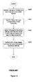
- Fig. 13 illustrates a flow chart of this systematic way.
- S200 the device layout is examined, to identify a critical pitch (S202). Accordingly, adjustment is made to NA, sigma outer, and sigma inner parameters for a given lithographic apparatus (S204). Based on these parameters, an aerial image may be generated by a simulator for a given mask pattern to identify significant proximity effects for the given pattern. These effects may be addressed by scatter bar treatment to the mask, OPC treatment to adjust the pattern or a combination of both (S206).
- an optimized bias and OPC treatment is still dependent on the parameters of the given lithographic apparatus such as NA, sigma-outer and sigma-inner. If changed, the routine has to be repeated for the mask. Often, this trial and error process is very time consuming to manually perfect for a given mask, and is primarily dependent on the skill of the designer manually adjusting parameters of the lithographic apparatus and performing the various treatments for addressing optical proximity effects.
- the disclosed concepts include a method and program product of optimizing lithographic apparatus settings and optimizing optical proximity correction (OPC) based on these settings for a pattern to be formed over a surface of a substrate.
- Steps include identifying a critical dense pitch and corresponding to a first critical feature and a second critical feature; determining optimal lithographic apparatus settings for the critical feature; performing OPC based on an analysis of the critical feature; performing OPC adjustments on the other critical feature; and optimizing lithographic apparatus settings for the other critical feature.
- OPC and lithographic apparatus settings may be mutually optimized.
- the disclosed concepts further include an apparatus for optimizing lithographic apparatus settings and optimizing optical proximity correction (OPC) based on these settings for a pattern to be formed over a surface of a substrate.
- the apparatus includes a radiation system for supplying a projection beam, an illuminator for receiving the projection beam of radiation and projecting an adjusted beam of radiation a portion of a mask, wherein the illuminator has preset sigma-outer and preset sigma-inner parameters, and a projection system having a numerical aperture ("NA") for imaging a corresponding irradiated portion of a mask, onto a target portion of a substrate.
- NA numerical aperture
- NA, preset sigma-outer, and preset sigma-inner and OPC are mutually optimized for a plurality of features of the pattern including a critical feature.
- the apparatus further includes a computer system configured to determine the preset NA, preset sigma-outer and preset sigma-inner parameters by identifying the critical feature and a non-critical feature of the plurality of features, determining optimal NA, preset sigma-outer, and preset sigma-inner settings such that the critical feature will print without bias adjustment, performing OPC based on an analysis of the critical feature, performing OPC adjustments on the non-critical feature, and optimizing NA, preset sigma-outer, and preset sigma-inner settings for the other feature.
- Fig. 1 schematically depicts a lithographic projection apparatus suitable for use following the concepts discussed herein.
- the apparatus comprises:
- the apparatus is of a transmissive type (i.e., has a transmissive mask). However, in general, it may also be of a reflective type, for example (with a reflective mask). Alternatively, the apparatus may employ another kind of patterning means as an alternative to the use of a mask; examples include a programmable mirror array or LCD matrix.
- the source LA (e.g. , a mercury lamp or excimer laser) produces a beam of radiation.
- This beam is fed into an illumination system (illuminator) IL, either directly or after having traversed conditioning means, such as a beam expander Ex, for example.
- the illuminator IL may comprise adjusting means AM for setting the outer and/or inner radial extent (commonly referred to as ⁇ -outer and ⁇ -inner, respectively) of the intensity distribution in the beam.
- ⁇ -outer and ⁇ -inner commonly referred to as ⁇ -outer and ⁇ -inner, respectively
- it will generally comprise various other components, such as an integrator IN and a condenser CO.
- the beam PB impinging on the mask MA has a desired uniformity and intensity distribution in its cross-section.
- the source LA may be within the housing of the lithographic projection apparatus (as is often the case when the source LA is a mercury lamp, for example), but that it may also be remote from the lithographic projection apparatus, the radiation beam that it produces being led into the apparatus ( e.g. , with the aid of suitable directing mirrors); this latter scenario is often the case when the source LA is an excimer laser (e.g. , based on KrF, ArF or F 2 lasing).
- the embodiments discussed herein encompasses at least both of these scenarios.
- the beam PB subsequently intercepts the mask MA, which is held on a mask table MT. Having traversed the mask MA, the beam PB passes through the lens PL, which focuses the beam PB onto a target portion C of the substrate W. With the aid of the second positioning means (and interferometric measuring means IF), the substrate table WT can be moved accurately, e.g. so as to position different target portions C in the path of the beam PB. Similarly, the first positioning means can be used to accurately position the mask MA with respect to the path of the beam PB, e.g. , after mechanical retrieval of the mask MA from a mask library, or during a scan.
- the mask table MT may just be connected to a short stroke actuator, or may be fixed.
- the depicted tool can be used in two different modes:
- the concepts disclosed herein may simulate or mathematically model any generic imaging system for imaging sub wavelength features, and may be especially useful with emerging imaging technologies capable of producing wavelengths of an increasingly smaller size.
- Emerging technologies already in use include EUV (extreme ultra violet) lithography that is capable of producing a 193nm wavelength with the use of a ArF laser, and even a 157nm wavelength with the use of a Fluorine laser.
- EUV lithography is capable of producing wavelengths within a range of 20-5nm by using a synchrotron or by hitting a material (either solid or a plasma) with high energy electrons in order to produce photons within this range.
- illumination may be produced by reflective mirrors with a multi-stack of Molybdenum and Silicon.
- the multi-stack mirror has a 40 layer pairs of Molybdenum and Silicon where the thickness of each layer is a quarter wavelength. Even smaller wavelengths may be produced with X-ray lithography.
- a synchrotron is used to produce an X-ray wavelength. Since most material is absorptive at x-ray wavelengths, a thin piece of absorbing material defines where features would print (positive resist) or not print (negative resist).
- Step 100 a pattern or portion thereof (hereinafter, "selected design") to be formed on a surface of a substrate is selected for analysis, and an interval or pitch analysis is performed on the selected design.
- An interval may be defined as a distance from an edge of a feature to another edge of another feature.
- a pitch may be defined as an interval plus feature width. In other words, interval relates to the distance between two features, whereas a pitch corresponds to the distance between two features plus the width of each feature.
- critical dense pitch corresponds to the smallest line width and interval in a design.
- interval or pitch analysis entails identifying the distribution of intervals or pitches for a selected design. Since pitch includes line width and interval, and because in a IC design the smallest line widths is specified by the design rule, results of an interval analysis can be easily converted to that which would result from a pitch analysis, and vice-versa. Therefore, for ease of explanation, the following will describe an interval analysis. But, in no way shall this disclosure be limited to an interval analysis.
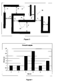
- Figure 3 illustrates an exemplary selected design.
- the intervals and pitches described herein are not limited to the selected design illustrated, and may include other designs incorporating contact holes or designs incorporating lines and contact hole(s).
- Intervals A, B, C, D, E, and F represent intervals having different numerical values. Any of numerous methods may be utilized for performing an interval analysis (S100) to identify the intervals A-F illustrated by Figure 3. The method may include manually inspecting the selected design to identify each interval and to determine its value. Perhaps a simpler technique would entail using a mask simulation program. Such an exemplary software program is MASKWEAVER from ASML MaskTools that is capable of examining any selected design and identifying and grouping like intervals.
- interval A corresponds to the critical dense pitch, i.e., the smallest combined interval and line width. It follows that feature 30 corresponds to the critical feature.
- lithographic apparatus settings may be iteratively adjusted until critical feature 30 prints without the need for bias adjustment.
- the inventors have found that the NA and sigma (sigma-outer and sigma-inner) may be adjusted to cause a critical feature to print with or without bias adjustment.
- any bias adjustment to a critical feature may worsen the optical proximity affects, and is often difficult to perform.
- lithographic apparatus settings i.e. , exposure dose, NA, sigma-outer, and sigma-inner
- lithographic apparatus settings is a simple way for causing the critical feature to print.
- NA and sigma are known to those of ordinary skill in lithograph art. Perhaps the best way for adjusting these parameters may be accomplished by utilizing a simulation software package such as Lithocruiser from ASML MaskTools that automatically determines an optimal NA and sigma such that the critical feature will print. Of course, a skilled lithographer could manually and iteratively adjust these parameters until a suitable exposure dose is determined for printing the critical feature. In any event, optimal lithographic apparatus parameters, such as NA optimal , sigma-outer optimal and sigma-inner optimal , may be determined such that bias adjustment B A is not required for feature 30 to print.
- a simulation software package such as Lithocruiser from ASML MaskTools that automatically determines an optimal NA and sigma such that the critical feature will print.
- a skilled lithographer could manually and iteratively adjust these parameters until a suitable exposure dose is determined for printing the critical feature.
- optimal lithographic apparatus parameters such as NA optimal , sigma-outer optimal and sigma-inner
- the "most" critical feature is identified and in most cases will corresponds to the smallest pitch, and optimal exposure dose parameters may be determined.
- the other critical pitch(s) may be overcome by adjusting bias B.
- SB scatter bar
- an OPC analysis is performed on the selected design shown in Fig. 3 that generates rules for intervals A - F, based on the guided estimation provided in S106.
- Techniques for generating SB rules through an OPC analysis are known to those of ordinary skill in the lithography art, and will require input of known lithographic apparatus parameters. These may include the numerical aperture ("NA") of the lens of a lithographic apparatus and sigma-outer and sigma-inner, which were discussed in connection to Fig. 1.
- NA numerical aperture
- OPC rules may be generated for each interval which specifies SB placement (x,y), SB Width (W), SB length (L), how many SB and any bias adjustment (B) for each interval.
- results of the OPC analysis may be tabulated, as shown by Table 2. There is no bias adjustment required on the critical feature 30, which corresponds to interval A.
- Fig. 4 illustrates an exemplary histogram that may be generated for the selected design of Fig. 3.
- the x-axis indicates intervals A - F and the y-axis indicates the frequency of each interval A-F.
- this chart identifies the interval amounts in the design for optimizing the SB placement (x,y), SB Width (W), SB length (L), how many SB and any bias adjustment (B) for each interval. Without this analysis, a skilled lithographer may miss some intervals that is critical for the design to get properly printed on wafer.
- OPC adjustments are performed on the features other than the critical feature 30.
- Techniques for performing OPC adjustments are known to those of ordinary skill in the art. A brief description will be given.
- the inventors have found that the actual process window is substantially smaller, when taking into consideration other features (including the critical feature) in the design. Thus, the inventors have found that further enhancement of the lithographic apparatus settings, and OPC treatment, will increase the process window for multiple features.
- Equation 1 is a cost function that factors in the difference or deviation between a predicted critical dimension (CD) and targeted CD for determining an optimal bias value. Other cost functions may be utilized for determining an optimal bias value. However, Equation 1 is useful for gradient based methods.
- Equation 2 represents a cost function for determining optimal scattering bar placements.
- OPC adjustments it is determined whether OPC adjustments are sufficient.
- the sufficiency of the OPC adjustments in S110 may be considered by examining any increase in the process window with the newly optimized settings.
- a lithographer may set a target process window for the entire design. For example, a designer may set a target process window for multiple features to be at least 75% area of the process window taking into consideration only the critical feature 30 or specify a specific depth of focus (DOF) at certain value of exposure latitude (EL).
- DOE depth of focus
- lithographic apparatus settings are further optimized based on the mask design which has been OPC-adjusted in step S110. newly selected feature. S108 and S110 will be repeated until sufficient OPC treatment has been accomplished. As opposed to optimizing lithographic apparatus settings for just the critical feature, lithographic apparatus settings may be optimized for multiple features (i.e., the entire mask design).
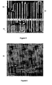
- Fig. 5 illustrates an exemplary target pattern.
- Reference numeral 50 denotes a critical feature (corresponding to the critical pitch of 320nm), and reference numerals 52 and 54 denote other semi-isolated features other than the critical features.
- Critical features 50 were identified corresponding to S100 and S102 (Fig. 2).
- the exemplary pattern of Fig. 5 was illuminated using Quasar illumination having the parameters listed in Table 4. Quasar Illumination Parameter Setting Wavelength 0.248 NA 0.7 Sigma Outer 0.85 Sigma Inner 0.55
- lithographic apparatus settings may be optimized for the critical feature 50.
- Table 5 list the optimized parameters in accordance with S106, and corresponding process window area. Optimized Quasar Illumination for CF 50 Parameter Setting Wavelength 0.248 NA 0.77 Sigma Outer 0.76 Sigma Inner 0.52 Process Window Area 1194.589573
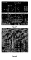
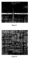
- Fig. 7 illustrates the process window 70 for multiple cut lines 50, 52, 54, which are illustrated by Fig. 5.
- the process window 70 decreases in size as compared to the process window 60 of Fig. 6.
- the area of process window 60 is dramatically reduced to 323.64918 (nm x mj/cm2).
- Figs. 8 and 9 are illustrative of the robustness of a lithographic apparatus that may have variations in exposure settings and focus. Ideally, any variations should cause corresponding variations within the critical dimension control specification.
- CD becomes bimodal in accordance with a variation of exposure settings and focus and there are CD value fall outside of the specification. This is caused by operation outside of the process window 70, also shown by Fig. 9.
- Further plotted on the graph of Fig. 9 is a plurality of CD values in accordance with a variation of exposure settings and focus. Ideally, the CD values should remain within process window 70. It is readily apparent that this is not the case.
- This is one of the problems that the disclosed concepts overcome by mutually optimizing exposure settings and OPC adjustments for a plurality of features including the critical feature 50.
- Figs. 8 and 9 are illustrative of insufficient OPC adjustments determined in S112.
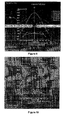
- Fig. 10 is a prime illustration of the process window for exposure settings and OPC mutually optimized for a plurality of features 50, 52, 54 including the critical feature 50.
- Table 6 lists the corresponding optimized exposure settings.
- the process window area has been increased by almost 300% as compared to the process window (Fig. 7).
- Figs. 11 and 12 are illustrative of the optimized robustness of a lithographic apparatus that may have variations in exposure settings and focus variations. Again, any variations should cause corresponding variations in the critical dimension.
- CD somewhat symmetrically changes with variations of exposure settings and focus, because operation is within process window 100, also shown by Fig. 12.
- Further plotted on the graph of Fig. 12 is a plurality of CD values in accordance with a variation of exposure settings and focus.
- Software may implement or aid in performing the disclosed concepts.
- Software functionalities of a computer system involve programming, including executable code, may be used to implement the above described optimization techniques.
- the software code is executable by the general-purpose computer.
- the code and possibly the associated data records are stored within a general-purpose computer platform.
- the software may be stored at other locations and/or transported for loading into the appropriate general-purpose computer systems.
- the embodiments discussed above involve one or more software products in the form of one or more modules of code carried by at least one machine-readable medium. Execution of such code by a processor of the computer system enables the platform to implement the catalogue and/or software downloading functions, in essentially the manner performed in the embodiments discussed and illustrated herein.
- Non-volatile media include, for example, optical or magnetic disks, such as any of the storage devices in any computer(s) operating as one of the server platform, discussed above.
- Volatile media include dynamic memory, such as main memory of such a computer platform.
- Physical transmission media include coaxial cables; copper wire and fibre optics, including the wires that comprise a bus within a computer system.
- Carrier-wave transmission media can take the form of electric or electromagnetic signals, or acoustic or light waves such as those generated during radio frequency (RF) and infrared (IR) data communications.
- Common forms of computer-readable media therefore include, for example: a floppy disk, a flexible disk, hard disk, magnetic tape, any other magnetic medium, a CD-ROM, DVD, any other optical medium, less commonly used media such as punch cards, paper tape, any other physical medium with patterns of holes, a RAM, a PROM, and EPROM, a FLASH-EPROM, any other memory chip or cartridge, a carrier wave transporting data or instructions, cables or links transporting such a carrier wave, or any other medium from which a computer can read programming code and/or data.
- Many of these forms of computer readable media may be involved in carrying one or more sequences of one or more instructions to a processor for execution.
Landscapes
- Physics & Mathematics (AREA)
- General Physics & Mathematics (AREA)
- Engineering & Computer Science (AREA)
- Condensed Matter Physics & Semiconductors (AREA)
- Manufacturing & Machinery (AREA)
- Computer Hardware Design (AREA)
- Microelectronics & Electronic Packaging (AREA)
- Power Engineering (AREA)
- Exposure And Positioning Against Photoresist Photosensitive Materials (AREA)
- Exposure Of Semiconductors, Excluding Electron Or Ion Beam Exposure (AREA)
- Preparing Plates And Mask In Photomechanical Process (AREA)
Applications Claiming Priority (2)
| Application Number | Priority Date | Filing Date | Title |
|---|---|---|---|
| US48310203P | 2003-06-30 | 2003-06-30 | |
| US483102P | 2003-06-30 |
Publications (2)
| Publication Number | Publication Date |
|---|---|
| EP1500974A2 true EP1500974A2 (fr) | 2005-01-26 |
| EP1500974A3 EP1500974A3 (fr) | 2006-04-12 |
Family
ID=33490761
Family Applications (1)
| Application Number | Title | Priority Date | Filing Date |
|---|---|---|---|
| EP04253958A Withdrawn EP1500974A3 (fr) | 2003-06-30 | 2004-06-30 | Méthode, programme et appareil pour l'optimalisation simultanée des réglages des conditions d'exposition NA-sigma et de la correction d'effets de proximité optiques utilisant des motifs auxiliaires |
Country Status (7)
| Country | Link |
|---|---|
| US (1) | US7355673B2 (fr) |
| EP (1) | EP1500974A3 (fr) |
| JP (2) | JP2005026701A (fr) |
| KR (2) | KR101096143B1 (fr) |
| CN (1) | CN1577099B (fr) |
| SG (1) | SG137686A1 (fr) |
| TW (1) | TWI345074B (fr) |
Cited By (5)
| Publication number | Priority date | Publication date | Assignee | Title |
|---|---|---|---|---|
| US7971160B2 (en) | 2005-07-22 | 2011-06-28 | Fujitsu Semiconductor Limited | Creating method of photomask pattern data, photomask created by using the photomask pattern data, and manufacturing method of semiconductor apparatus using the photomask |
| CN102289156A (zh) * | 2011-08-14 | 2011-12-21 | 北京理工大学 | 一种光刻机NA-Sigma配置的优化方法 |
| US8085386B2 (en) | 2006-12-22 | 2011-12-27 | Canon Kabushiki Kaisha | Method for determining exposure condition and computer-readable storage media storing program for determining exposure condition |
| US8302061B2 (en) | 2005-05-20 | 2012-10-30 | Cadence Design Systems, Inc. | Aware manufacturing of an integrated circuit |
| US8713484B2 (en) | 2005-05-20 | 2014-04-29 | Cadence Design Systems, Inc. | Aware manufacturing of integrated circuits |
Families Citing this family (48)
| Publication number | Priority date | Publication date | Assignee | Title |
|---|---|---|---|---|
| US20050073671A1 (en) * | 2003-10-07 | 2005-04-07 | Intel Corporation | Composite optical lithography method for patterning lines of substantially equal width |
| US20050074698A1 (en) * | 2003-10-07 | 2005-04-07 | Intel Corporation | Composite optical lithography method for patterning lines of significantly different widths |
| US20050085085A1 (en) * | 2003-10-17 | 2005-04-21 | Yan Borodovsky | Composite patterning with trenches |
| US7142282B2 (en) * | 2003-10-17 | 2006-11-28 | Intel Corporation | Device including contacts |
| US20050088633A1 (en) * | 2003-10-24 | 2005-04-28 | Intel Corporation | Composite optical lithography method for patterning lines of unequal width |
| WO2005055295A1 (fr) * | 2003-12-03 | 2005-06-16 | Nikon Corporation | Procede et systeme d'exposition, et procede de production d'un dispositif |
| US6977715B2 (en) * | 2004-05-19 | 2005-12-20 | Nanya Technology Corp. | Method for optimizing NILS of exposed lines |
| KR100653990B1 (ko) * | 2004-12-29 | 2006-12-05 | 주식회사 하이닉스반도체 | 포토마스크 데이터베이스 패턴의 불량 검사 방법 |
| KR100636677B1 (ko) | 2005-04-04 | 2006-10-23 | 주식회사 하이닉스반도체 | 이방성 및 비대칭 조명을 이용한 노광공정에서의레이아웃체크방법 |
| JP4336671B2 (ja) | 2005-07-15 | 2009-09-30 | キヤノン株式会社 | 露光パラメータの決定をコンピュータに実行させるプログラム、露光パラメータを決定する決定方法、露光方法及びデバイス製造方法。 |
| JP5147167B2 (ja) * | 2005-07-29 | 2013-02-20 | キヤノン株式会社 | 決定方法及びプログラム |
| US20070046917A1 (en) * | 2005-08-31 | 2007-03-01 | Asml Netherlands B.V. | Lithographic apparatus and device manufacturing method that compensates for reticle induced CDU |
| US20070092844A1 (en) * | 2005-10-21 | 2007-04-26 | Macronix International Co., Ltd. | Method to form photo patterns |
| KR100673014B1 (ko) | 2005-10-28 | 2007-01-24 | 삼성전자주식회사 | 포토 마스크의 제조 방법 |
| EP1873663A1 (fr) | 2006-06-27 | 2008-01-02 | Takumi Technology Corporation | Procédé d'optimisation du tracé physique du circuit intégré |
| KR100800685B1 (ko) * | 2006-12-28 | 2008-02-01 | 동부일렉트로닉스 주식회사 | 모델 기반 opc를 통한 시그마 매칭 방법 |
| JP4997006B2 (ja) * | 2007-07-18 | 2012-08-08 | ルネサスエレクトロニクス株式会社 | 反射型露光方法 |
| KR100864934B1 (ko) * | 2007-08-20 | 2008-10-22 | 주식회사 동부하이텍 | 마스크 레이아웃 보정 방법 및 마스크 레이아웃 보정 장치 |
| NL1036335A1 (nl) * | 2007-12-27 | 2009-06-30 | Asml Netherlands Bv | Device manufacturing method, lithographic system, lithographic apparatus and design for manufacturing system. |
| JP5909219B2 (ja) * | 2008-06-06 | 2016-04-26 | 株式会社東芝 | マスクパターンデータ作成方法、マスクパターンデータ作成プログラム、マスク、半導体装置の製造方法 |
| JP4843649B2 (ja) * | 2008-08-07 | 2011-12-21 | 株式会社東芝 | 評価パターン作成方法、評価パターン作成プログラムおよびパターン検証方法 |
| US8103979B2 (en) * | 2008-10-20 | 2012-01-24 | Advanced Micro Devices, Inc. | System for generating and optimizing mask assist features based on hybrid (model and rules) methodology |
| CN102224459B (zh) | 2008-11-21 | 2013-06-19 | Asml荷兰有限公司 | 用于优化光刻过程的方法及设备 |
| NL2003699A (en) | 2008-12-18 | 2010-06-21 | Brion Tech Inc | Method and system for lithography process-window-maximixing optical proximity correction. |
| JP5607348B2 (ja) * | 2009-01-19 | 2014-10-15 | キヤノン株式会社 | 原版データを生成する方法およびプログラム、ならびに、原版製作方法 |
| JP4838866B2 (ja) * | 2009-02-10 | 2011-12-14 | キヤノン株式会社 | 露光パラメータ及びレチクルパターンを決定する決定方法、露光方法及びデバイス製造方法。 |
| CN101893820B (zh) * | 2009-05-22 | 2012-06-27 | 中芯国际集成电路制造(北京)有限公司 | 光学邻近修正的方法 |
| US8321818B2 (en) * | 2009-06-26 | 2012-11-27 | International Business Machines Corporation | Model-based retargeting of layout patterns for sub-wavelength photolithography |
| US8146026B2 (en) | 2009-11-17 | 2012-03-27 | International Business Machines Corporation | Simultaneous photolithographic mask and target optimization |
| US8230372B2 (en) * | 2009-12-03 | 2012-07-24 | International Business Machines Corporation | Retargeting for electrical yield enhancement |
| US8331646B2 (en) | 2009-12-23 | 2012-12-11 | International Business Machines Corporation | Optical proximity correction for transistors using harmonic mean of gate length |
| NL2005804A (en) * | 2010-01-14 | 2011-07-18 | Asml Netherlands Bv | Method and apparatus for enhancing signal strength for improved generation and placement of model-based sub-resolution assist features (mb-sraf). |
| JP5627394B2 (ja) * | 2010-10-29 | 2014-11-19 | キヤノン株式会社 | マスクのデータ及び露光条件を決定するためのプログラム、決定方法、マスク製造方法、露光方法及びデバイス製造方法 |
| NL2007642A (en) * | 2010-11-10 | 2012-05-14 | Asml Netherlands Bv | Optimization flows of source, mask and projection optics. |
| JP5673947B2 (ja) * | 2011-03-01 | 2015-02-18 | 大日本印刷株式会社 | マスクパターンの補正方法、プログラム及び該補正方法を用いたフォトマスク |
| JP5835968B2 (ja) * | 2011-07-05 | 2015-12-24 | キヤノン株式会社 | 決定方法、プログラム及び露光方法 |
| CN102253607B (zh) * | 2011-08-15 | 2012-10-10 | 北京理工大学 | 一种光刻机照明系统相干因子的优化方法 |
| EP2570854B1 (fr) | 2011-09-16 | 2016-11-30 | Imec | Définition de la forme d'une source d'éclairage en lithographie optique |
| JP6003068B2 (ja) * | 2012-01-30 | 2016-10-05 | 富士通セミコンダクター株式会社 | 露光方法 |
| JP5869942B2 (ja) * | 2012-04-03 | 2016-02-24 | インターナショナル・ビジネス・マシーンズ・コーポレーションInternational Business Machines Corporation | マスクのデザイン方法、プログラムおよびマスクデザインシステム |
| WO2014192518A1 (fr) | 2013-05-27 | 2014-12-04 | インターナショナル・ビジネス・マシーンズ・コーポレーション | Source de lumière d'exposition, procédé et programme de conception de masque |
| JP6418786B2 (ja) * | 2013-07-10 | 2018-11-07 | キヤノン株式会社 | パターンの作成方法、プログラムおよび情報処理装置 |
| US9026956B1 (en) | 2013-10-11 | 2015-05-05 | Taiwan Semiconductor Manufacturing Co., Ltd. | Method of lithographic process evaluation |
| CN104635417B (zh) * | 2013-11-14 | 2018-06-01 | 中芯国际集成电路制造(上海)有限公司 | 偏差修正方法 |
| JP7081490B2 (ja) * | 2016-09-27 | 2022-06-07 | 株式会社ニコン | レイアウト情報提供方法、レイアウト情報、決定方法、プログラム、並びに情報記録媒体 |
| CN107103145B (zh) * | 2017-05-08 | 2020-11-20 | 上海华力微电子有限公司 | 计算版图中线宽固定节距不同的线条的分布的方法 |
| KR20210028798A (ko) | 2019-09-04 | 2021-03-15 | 삼성전자주식회사 | 반도체 장치의 제조 방법 |
| CN113031388A (zh) * | 2021-02-26 | 2021-06-25 | 广东省大湾区集成电路与系统应用研究院 | 光学邻近效应修正中散射条的嵌入方法 |
Citations (5)
| Publication number | Priority date | Publication date | Assignee | Title |
|---|---|---|---|---|
| US5447810A (en) * | 1994-02-09 | 1995-09-05 | Microunity Systems Engineering, Inc. | Masks for improved lithographic patterning for off-axis illumination lithography |
| EP1237046A2 (fr) * | 2001-02-28 | 2002-09-04 | ASML Masktools B.V. | Méthode pour l identification des regions d interaction extrème, méthodes pour créer des motifs de masque et production de masques, méthodes pour la fabrication de dispositifs et programmes d'ordinateur |
| EP1239331A2 (fr) * | 2001-02-23 | 2002-09-11 | ASML Netherlands B.V. | Optimisation d illumination de motifs spécifiques |
| EP1308780A2 (fr) * | 2001-11-05 | 2003-05-07 | ASML Masktools B.V. | Méthode et apparail de fabrication de masques utilisés conjointement à des techniques d'illumination dipolaire |
| EP1357426A2 (fr) * | 2002-04-23 | 2003-10-29 | Canon Kabushiki Kaisha | Méthode pour déterminer l'arrangement de motifs sur un masque ainsi que les conditions d'exposition |
Family Cites Families (34)
| Publication number | Priority date | Publication date | Assignee | Title |
|---|---|---|---|---|
| US524270A (en) * | 1894-08-07 | Adjustable portable scaffold | ||
| US5523193A (en) * | 1988-05-31 | 1996-06-04 | Texas Instruments Incorporated | Method and apparatus for patterning and imaging member |
| DE59105735D1 (de) * | 1990-05-02 | 1995-07-20 | Fraunhofer Ges Forschung | Belichtungsvorrichtung. |
| US5229255A (en) * | 1991-03-22 | 1993-07-20 | At&T Bell Laboratories | Sub-micron device fabrication with a phase shift mask having multiple values of phase delay |
| JP3179520B2 (ja) * | 1991-07-11 | 2001-06-25 | 株式会社日立製作所 | 半導体装置の製造方法 |
| US5324600A (en) * | 1991-07-12 | 1994-06-28 | Oki Electric Industry Co., Ltd. | Method of forming resist pattern and photomask therefor |
| US5242770A (en) | 1992-01-16 | 1993-09-07 | Microunity Systems Engineering, Inc. | Mask for photolithography |
| US5229872A (en) * | 1992-01-21 | 1993-07-20 | Hughes Aircraft Company | Exposure device including an electrically aligned electronic mask for micropatterning |
| US5288569A (en) * | 1992-04-23 | 1994-02-22 | International Business Machines Corporation | Feature biassing and absorptive phase-shifting techniques to improve optical projection imaging |
| JP3203394B2 (ja) | 1992-06-19 | 2001-08-27 | 日本電信電話株式会社 | 投影光学系の設計方法 |
| US5256505A (en) * | 1992-08-21 | 1993-10-26 | Microunity Systems Engineering | Lithographical mask for controlling the dimensions of resist patterns |
| US5538815A (en) * | 1992-09-14 | 1996-07-23 | Kabushiki Kaisha Toshiba | Method for designing phase-shifting masks with automatization capability |
| JPH06120114A (ja) | 1992-10-06 | 1994-04-28 | Hitachi Ltd | 投影露光方法および装置 |
| JPH06163350A (ja) | 1992-11-19 | 1994-06-10 | Matsushita Electron Corp | 投影露光方法および装置 |
| JPH06181166A (ja) | 1992-12-14 | 1994-06-28 | Nikon Corp | 投影露光装置 |
| US5362584A (en) * | 1993-04-02 | 1994-11-08 | International Business Machines Corporation | Phase-shifting transparent lithographic mask for writing contiguous structures from noncontiguous mask areas |
| JP3283624B2 (ja) | 1993-04-12 | 2002-05-20 | 株式会社日立製作所 | ホトマスク |
| JPH07134395A (ja) * | 1993-04-22 | 1995-05-23 | Samsung Electron Co Ltd | マスクパターン及びこれを使用した微細パターンの形成方法 |
| JPH07134390A (ja) | 1993-06-14 | 1995-05-23 | Sony Corp | 露光装置の設計方法及び露光用マスクの設計方法 |
| US5424154A (en) * | 1993-12-10 | 1995-06-13 | Intel Corporation | Lithographic emhancement method and apparatus for randomly spaced structures |
| US5663893A (en) * | 1995-05-03 | 1997-09-02 | Microunity Systems Engineering, Inc. | Method for generating proximity correction features for a lithographic mask pattern |
| KR0161437B1 (ko) | 1995-09-19 | 1999-02-01 | 김광호 | 반도체장치의 미세패턴 형성방법 |
| JP2917879B2 (ja) * | 1995-10-31 | 1999-07-12 | 日本電気株式会社 | フォトマスク及びその製造方法 |
| US5723233A (en) * | 1996-02-27 | 1998-03-03 | Lsi Logic Corporation | Optical proximity correction method and apparatus |
| EP0824722B1 (fr) * | 1996-03-06 | 2001-07-25 | Asm Lithography B.V. | Systeme d'interferometre differentiel et dispositif lithographique a balayage par etapes pourvu d'un tel systeme |
| US5707765A (en) * | 1996-05-28 | 1998-01-13 | Microunity Systems Engineering, Inc. | Photolithography mask using serifs and method thereof |
| WO1998028665A1 (fr) * | 1996-12-24 | 1998-07-02 | Koninklijke Philips Electronics N.V. | Dispositif de positionnement bidimensionnellement equilibre a deux porte-objets, et dispositif lithographique comportant ledit dispositif |
| US5821014A (en) | 1997-02-28 | 1998-10-13 | Microunity Systems Engineering, Inc. | Optical proximity correction method for intermediate-pitch features using sub-resolution scattering bars on a mask |
| DE69829614T2 (de) | 1997-03-10 | 2006-03-09 | Asml Netherlands B.V. | Lithographiegerät mit einer positioniervorrichtung mit zwei objekthaltern |
| US6114071A (en) * | 1997-11-24 | 2000-09-05 | Asml Masktools Netherlands B.V. | Method of fine feature edge tuning with optically-halftoned mask |
| JP4352498B2 (ja) * | 1999-03-26 | 2009-10-28 | ソニー株式会社 | パターン露光方法とこれに用いる処理装置 |
| TWI232356B (en) | 2000-09-04 | 2005-05-11 | Asml Netherlands Bv | Lithographic projection apparatus, device manufacturing method and device manufactured thereby |
| GB2367907A (en) * | 2000-10-13 | 2002-04-17 | Mitel Semiconductor Ltd | Optical proximity correction |
| US6792591B2 (en) * | 2001-02-28 | 2004-09-14 | Asml Masktools B.V. | Method of identifying an extreme interaction pitch region, methods of designing mask patterns and manufacturing masks, device manufacturing methods and computer programs |
-
2004
- 2004-06-29 US US10/878,489 patent/US7355673B2/en active Active
- 2004-06-30 KR KR1020040050283A patent/KR101096143B1/ko not_active IP Right Cessation
- 2004-06-30 CN CN2004100552728A patent/CN1577099B/zh not_active Expired - Fee Related
- 2004-06-30 TW TW093119582A patent/TWI345074B/zh not_active IP Right Cessation
- 2004-06-30 SG SG200403810-5A patent/SG137686A1/en unknown
- 2004-06-30 JP JP2004220964A patent/JP2005026701A/ja active Pending
- 2004-06-30 EP EP04253958A patent/EP1500974A3/fr not_active Withdrawn
-
2010
- 2010-01-27 JP JP2010015603A patent/JP2010146024A/ja active Pending
-
2011
- 2011-10-21 KR KR1020110108183A patent/KR101185463B1/ko not_active IP Right Cessation
Patent Citations (5)
| Publication number | Priority date | Publication date | Assignee | Title |
|---|---|---|---|---|
| US5447810A (en) * | 1994-02-09 | 1995-09-05 | Microunity Systems Engineering, Inc. | Masks for improved lithographic patterning for off-axis illumination lithography |
| EP1239331A2 (fr) * | 2001-02-23 | 2002-09-11 | ASML Netherlands B.V. | Optimisation d illumination de motifs spécifiques |
| EP1237046A2 (fr) * | 2001-02-28 | 2002-09-04 | ASML Masktools B.V. | Méthode pour l identification des regions d interaction extrème, méthodes pour créer des motifs de masque et production de masques, méthodes pour la fabrication de dispositifs et programmes d'ordinateur |
| EP1308780A2 (fr) * | 2001-11-05 | 2003-05-07 | ASML Masktools B.V. | Méthode et apparail de fabrication de masques utilisés conjointement à des techniques d'illumination dipolaire |
| EP1357426A2 (fr) * | 2002-04-23 | 2003-10-29 | Canon Kabushiki Kaisha | Méthode pour déterminer l'arrangement de motifs sur un masque ainsi que les conditions d'exposition |
Cited By (7)
| Publication number | Priority date | Publication date | Assignee | Title |
|---|---|---|---|---|
| US8302061B2 (en) | 2005-05-20 | 2012-10-30 | Cadence Design Systems, Inc. | Aware manufacturing of an integrated circuit |
| US8713484B2 (en) | 2005-05-20 | 2014-04-29 | Cadence Design Systems, Inc. | Aware manufacturing of integrated circuits |
| US7971160B2 (en) | 2005-07-22 | 2011-06-28 | Fujitsu Semiconductor Limited | Creating method of photomask pattern data, photomask created by using the photomask pattern data, and manufacturing method of semiconductor apparatus using the photomask |
| DE112005003638B4 (de) | 2005-07-22 | 2018-10-25 | Fujitsu Semiconductor Ltd. | Verfahren zur Erstellung von Fotomaskenstrukturdaten und Verfahren zur Herstellung einer Halbleitervorrichtung |
| US8085386B2 (en) | 2006-12-22 | 2011-12-27 | Canon Kabushiki Kaisha | Method for determining exposure condition and computer-readable storage media storing program for determining exposure condition |
| CN102289156A (zh) * | 2011-08-14 | 2011-12-21 | 北京理工大学 | 一种光刻机NA-Sigma配置的优化方法 |
| CN102289156B (zh) * | 2011-08-14 | 2013-06-05 | 北京理工大学 | 一种光刻机NA-Sigma配置的优化方法 |
Also Published As
| Publication number | Publication date |
|---|---|
| TWI345074B (en) | 2011-07-11 |
| KR20050002650A (ko) | 2005-01-07 |
| KR101185463B1 (ko) | 2012-10-02 |
| SG137686A1 (en) | 2007-12-28 |
| KR20110133520A (ko) | 2011-12-13 |
| KR101096143B1 (ko) | 2011-12-19 |
| US20050028129A1 (en) | 2005-02-03 |
| JP2010146024A (ja) | 2010-07-01 |
| CN1577099A (zh) | 2005-02-09 |
| TW200525178A (en) | 2005-08-01 |
| JP2005026701A (ja) | 2005-01-27 |
| EP1500974A3 (fr) | 2006-04-12 |
| CN1577099B (zh) | 2010-05-05 |
| US7355673B2 (en) | 2008-04-08 |
Similar Documents
| Publication | Publication Date | Title |
|---|---|---|
| US7355673B2 (en) | Method, program product and apparatus of simultaneous optimization for NA-Sigma exposure settings and scattering bars OPC using a device layout | |
| US7349066B2 (en) | Apparatus, method and computer program product for performing a model based optical proximity correction factoring neighbor influence | |
| US7355681B2 (en) | Optical proximity correction using chamfers and rounding at corners | |
| US7681171B2 (en) | Method, program product and apparatus for performing double exposure lithography | |
| US7138212B2 (en) | Method and apparatus for performing model-based layout conversion for use with dipole illumination | |
| US7485396B2 (en) | Scattering bar OPC application method for sub-half wavelength lithography patterning | |
| EP1630601A2 (fr) | Procédé de fabrication d'une ébauche de masque, procédé de correction de l'effet de proximité optique, procédé de fabrication d'un dispositif, programme d'ordinateur et support de stockage lisible par ordinateur | |
| EP1385053A2 (fr) | Création de règles pour la correction de l'effet de proximité optique (OPC) | |
| US7514183B2 (en) | Method for performing transmission tuning of a mask pattern to improve process latitude | |
| US7433791B2 (en) | Method of performing multiple stage model calibration for optical imaging simulation models | |
| US7856606B2 (en) | Apparatus, method and program product for suppressing waviness of features to be printed using photolithographic systems | |
| US7804646B2 (en) | Method for decomposition of a customized DOE for use with a single exposure into a set of multiple exposures using standard DOEs with optimized exposure settings |
Legal Events
| Date | Code | Title | Description |
|---|---|---|---|
| PUAI | Public reference made under article 153(3) epc to a published international application that has entered the european phase |
Free format text: ORIGINAL CODE: 0009012 |
|
| AK | Designated contracting states |
Kind code of ref document: A2 Designated state(s): AT BE BG CH CY CZ DE DK EE ES FI FR GB GR HU IE IT LI LU MC NL PL PT RO SE SI SK TR |
|
| AX | Request for extension of the european patent |
Extension state: AL HR LT LV MK |
|
| PUAL | Search report despatched |
Free format text: ORIGINAL CODE: 0009013 |
|
| AK | Designated contracting states |
Kind code of ref document: A3 Designated state(s): AT BE BG CH CY CZ DE DK EE ES FI FR GB GR HU IE IT LI LU MC NL PL PT RO SE SI SK TR |
|
| AX | Request for extension of the european patent |
Extension state: AL HR LT LV MK |
|
| 17P | Request for examination filed |
Effective date: 20060914 |
|
| AKX | Designation fees paid |
Designated state(s): DE FR GB IT NL |
|
| 17Q | First examination report despatched |
Effective date: 20061124 |
|
| STAA | Information on the status of an ep patent application or granted ep patent |
Free format text: STATUS: THE APPLICATION IS DEEMED TO BE WITHDRAWN |
|
| 18D | Application deemed to be withdrawn |
Effective date: 20090728 |