The technical field relates generally to a method, program product, and apparatus for
microlithography for optimizing lithographic apparatus settings, and optimizing optical
proximity correction (OPC).
Lithographic apparatus can be used, for example, in the manufacture of integrated
circuits (ICs). In such a case, the mask may contain a circuit pattern corresponding to an
individual layer of the IC, and this pattern can be imaged onto a target portion (e.g.
comprising one or more dies) on a substrate (silicon wafer) that has been coated with a layer
of radiation-sensitive material (resist). In general, a single wafer will contain a whole
network of adjacent target portions that are successively irradiated via the projection system,
one at a time. In one type of lithographic projection apparatus, each target portion is
irradiated by exposing the entire mask pattern onto the target portion in one go; such an
apparatus is commonly referred to as a wafer stepper. In an alternative apparatus, commonly
referred to as a step-and-scan apparatus, each target portion is irradiated by progressively
scanning the mask pattern under the projection beam in a given reference direction (the
"scanning" direction) while synchronously scanning the substrate table parallel or anti-parallel
to this direction. Since, in general, the projection system will have a magnification factor M
(generally < 1), the speed V at which the substrate table is scanned will be a factor M times
that at which the mask table is scanned. More information with regard to lithographic devices
as described herein can be gleaned, for example, from US 6,046,792, incorporated herein by
reference.
In a manufacturing process using a lithographic projection apparatus, a mask pattern is
imaged onto a substrate that is at least partially covered by a layer of radiation-sensitive
material (resist). Prior to this imaging step, the substrate may undergo various procedures,
such as priming, resist coating and a soft bake. After exposure, the substrate may be
subjected to other procedures, such as a post-exposure bake (PEB), development, a hard bake
and measurement/inspection of the imaged features. This array of procedures is used as a
basis to pattern an individual layer of a device, e.g., an IC. Such a patterned layer may then
undergo various processes such as etching, ion-implantation (doping), metallization,
oxidation, chemo-mechanical polishing, etc., all intended to finish off an individual layer. If
several layers are required, then the whole procedure, or a variant thereof, will have to be
repeated for each new layer. Eventually, an array of devices will be present on the substrate
(wafer). These devices are then separated from one another by a technique such as dicing or
sawing, whence the individual devices can be mounted on a carrier, connected to pins, etc.
For the sake of simplicity, the projection system may hereinafter be referred to as the
"lens"; however, this term should be broadly interpreted as encompassing various types of
projection systems, including refractive optics, reflective optics, and catadioptric systems, for
example. The radiation system may also include components operating according to any of
these design types for directing, shaping or controlling the projection beam of radiation, and
such components may also be referred to below, collectively or singularly, as a "lens".
Further, the lithographic apparatus may be of a type having two or more substrate tables
(and/or two or more mask tables). In such "multiple stage" devices the additional tables may
be used in parallel, or preparatory steps may be carried out on one or more tables while one or
more other tables are being used for exposures. Twin stage lithographic apparatus are
described, for example, in US 5,969,441, incorporated herein by reference.
The photolithographic masks referred to above comprise geometric patterns
corresponding to the circuit components to be integrated onto a silicon wafer. The patterns
used to create such masks are generated utilizing CAD (computer-aided design) programs,
this process often being referred to as EDA (electronic design automation). Most CAD
programs follow a set of predetermined design rules in order to create functional masks.
These rules are set by processing and design limitations. For example, design rules define the
space tolerance between circuit devices (such as gates, capacitors, etc.) or interconnect lines,
so as to ensure that the circuit devices or lines do not interact with one another in an
undesirable way. The design rule limitations are typically referred to as "critical dimensions"
(CD). A critical dimension of a circuit can be defined as the smallest width of a line or hole
or the smallest space between two lines or two holes. Thus, the CD determines the overall
size and density of the designed circuit.
Of course, one of the goals in integrated circuit fabrication is to faithfully reproduce
the original circuit design on the wafer (via the mask). However, as the size of
lithographically fabricated structures decrease, and the density of the structures increases, the
cost and complexity of designing masks additionally increases. That is, as the demand
continues for higher performance of semiconductor devices, the design rule shrink rate is
outpacing the progress of both of the exposure wavelength reduction and the advancement of
high Numerical Aperture (NA) lenses. Therefore, resolution enhancement techniques have
been indispensable in low k1 systems. Types of enhancement techniques include optical
proximity correction (OPC) and the optimization of the lithographic apparatus, especially the
optimization of the NA and partial coherence factor (sigma). These techniques help to
overcome certain proximity effects; however, they are manually performed.
Moreover, OPC techniques include feature biasing and strategic placement of sub-lithographic
features on the original mask pattern to compensate for proximity effects, thereby
improving the final transferred circuit pattern. Sub-resolution assist features, or scattering
bars, have been used as a means to correct for optical proximity effects and have been shown
to be effective for increasing the overall process window (i.e., the ability to consistently print
features having a specified CD regardless of whether or not the features are isolated or
densely packed relative to adjacent features). The scattering bars function to change the
effective pattern density (of the isolated or less dense features) to be more dense, thereby
negating the undesirable proximity effects associated with printing of isolated or less dense
features.
For the intermediate pitch features pitches, where there is no room to insert a SB, a
typical method of optical proximity correction (OPC) is to adjust the feature edges (or apply
bias) so that the printed feature width is closer to the intended width. In order for the use of
the sub-resolution features and/or feature biasing to be effective for minimizing optical
proximity effects, an operator having a substantial amount of knowledge regarding mask
design and the printing process, as well as a substantial amount of experience, is required to
modify the mask design to include the subresolution features and/or the adjustment of feature
edges (biasing) if the desired goal is to be obtained. Indeed, even when an experienced
operator performs this task, it is often necessary to conduct a "trial and error" process in order
to properly position the subresolution features to obtain the desired corrections. This trial and
error process, which can entail repeated mask revisions followed by repeated simulations, can
become both a time consuming and costly process.
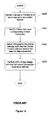
In accordance with the foregoing description, there develops a systematic way in
which designers optimize a mask pattern. Fig. 13 illustrates a flow chart of this systematic
way. In S200, the device layout is examined, to identify a critical pitch (S202). Accordingly,
adjustment is made to NA, sigma outer, and sigma inner parameters for a given lithographic
apparatus (S204). Based on these parameters, an aerial image may be generated by a
simulator for a given mask pattern to identify significant proximity effects for the given
pattern. These effects may be addressed by scatter bar treatment to the mask, OPC treatment
to adjust the pattern or a combination of both (S206). Still with scatter bar treatment and/or
OPC treatment, an optimized bias and OPC treatment is still dependent on the parameters of
the given lithographic apparatus such as NA, sigma-outer and sigma-inner. If changed, the
routine has to be repeated for the mask. Often, this trial and error process is very time
consuming to manually perfect for a given mask, and is primarily dependent on the skill of the
designer manually adjusting parameters of the lithographic apparatus and performing the
various treatments for addressing optical proximity effects.
Accordingly, there exists a need to create a method or routine that can optimize
lithographic apparatus parameters and optimally configure biasing utilizing OPC.
The disclosed concepts include a method and program product of optimizing
lithographic apparatus settings and optimizing optical proximity correction (OPC) based on
these settings for a pattern to be formed over a surface of a substrate. Steps include
identifying a critical dense pitch and corresponding to a first critical feature and a second
critical feature; determining optimal lithographic apparatus settings for the critical feature;
performing OPC based on an analysis of the critical feature; performing OPC adjustments on
the other critical feature; and optimizing lithographic apparatus settings for the other critical
feature. Advantageously, OPC and lithographic apparatus settings may be mutually
optimized.
The disclosed concepts further include an apparatus for optimizing lithographic
apparatus settings and optimizing optical proximity correction (OPC) based on these settings
for a pattern to be formed over a surface of a substrate. The apparatus includes a radiation
system for supplying a projection beam, an illuminator for receiving the projection beam of
radiation and projecting an adjusted beam of radiation a portion of a mask, wherein the
illuminator has preset sigma-outer and preset sigma-inner parameters, and a projection system
having a numerical aperture ("NA") for imaging a corresponding irradiated portion of a mask,
onto a target portion of a substrate. NA, preset sigma-outer, and preset sigma-inner and OPC
are mutually optimized for a plurality of features of the pattern including a critical feature.
The apparatus further includes a computer system configured to determine the preset NA,
preset sigma-outer and preset sigma-inner parameters by identifying the critical feature and a
non-critical feature of the plurality of features, determining optimal NA, preset sigma-outer,
and preset sigma-inner settings such that the critical feature will print without bias adjustment,
performing OPC based on an analysis of the critical feature, performing OPC adjustments on
the non-critical feature, and optimizing NA, preset sigma-outer, and preset sigma-inner
settings for the other feature.
The foregoing and other features, aspects, and advantages of the present disclosure
will become more apparent from the following detailed description when taken in conjunction
with the accompanying drawings, in which:
Fig. 1 schematically depicts a lithographic projection apparatus suitable for use
following the concepts discussed herein. The apparatus comprises:
- a radiation system Ex, IL, for supplying a projection beam PB of radiation. In this
particular case, the radiation system also comprises a radiation source LA;
- a first object table (mask table) MT provided with a mask holder for holding a mask
MA (e.g., a reticle), and connected to first positioning means for accurately positioning the
mask with respect to item PL;
- a second object table (substrate table) WT provided with a substrate holder for holding
a substrate W (e.g., a resist-coated silicon wafer), and connected to second positioning means
for accurately positioning the substrate with respect to item PL;
- a projection system ("lens") PL (e.g., a refractive, catoptric or catadioptric optical
system) for imaging an irradiated portion of the mask MA onto a target portion C (e.g.,
comprising one or more dies) of the substrate W. The projection system has an adjustable
numerical aperture ("NA").
As depicted herein, the apparatus is of a transmissive type (i.e., has a transmissive
mask). However, in general, it may also be of a reflective type, for example (with a reflective
mask). Alternatively, the apparatus may employ another kind of patterning means as an
alternative to the use of a mask; examples include a programmable mirror array or LCD
matrix.
The source LA (e.g., a mercury lamp or excimer laser) produces a beam of radiation.
This beam is fed into an illumination system (illuminator) IL, either directly or after having
traversed conditioning means, such as a beam expander Ex, for example. The illuminator IL
may comprise adjusting means AM for setting the outer and/or inner radial extent (commonly
referred to as σ-outer and σ-inner, respectively) of the intensity distribution in the beam. In
addition, it will generally comprise various other components, such as an integrator IN and a
condenser CO. In this way, the beam PB impinging on the mask MA has a desired uniformity
and intensity distribution in its cross-section.
It should be noted with regard to Figure 1 that the source LA may be within the
housing of the lithographic projection apparatus (as is often the case when the source LA is a
mercury lamp, for example), but that it may also be remote from the lithographic projection
apparatus, the radiation beam that it produces being led into the apparatus (e.g., with the aid
of suitable directing mirrors); this latter scenario is often the case when the source LA is an
excimer laser (e.g., based on KrF, ArF or F2 lasing). The embodiments discussed herein
encompasses at least both of these scenarios.
The beam PB subsequently intercepts the mask MA, which is held on a mask table
MT. Having traversed the mask MA, the beam PB passes through the lens PL, which focuses
the beam PB onto a target portion C of the substrate W. With the aid of the second
positioning means (and interferometric measuring means IF), the substrate table WT can be
moved accurately, e.g. so as to position different target portions C in the path of the beam PB.
Similarly, the first positioning means can be used to accurately position the mask MA with
respect to the path of the beam PB, e.g., after mechanical retrieval of the mask MA from a
mask library, or during a scan. In general, movement of the object tables MT, WT will be
realized with the aid of a long-stroke module (coarse positioning) and a short-stroke module
(fine positioning), which are not explicitly depicted in Fig. 28. However, in the case of a
wafer stepper (as opposed to a step-and-scan tool) the mask table MT may just be connected
to a short stroke actuator, or may be fixed.
The depicted tool can be used in two different modes:
- In step mode, the mask table MT is kept essentially stationary, and an entire mask
image is projected in one go (i.e., a single "flash") onto a target portion C. The substrate table
WT is then shifted in the x and/or y directions so that a different target portion C can be
irradiated by the beam PB;
- In scan mode, essentially the same scenario applies, except that a given target portion
C is not exposed in a single "flash". Instead, the mask table MT is movable in a given
direction (the so-called "scan direction", e.g., the y direction) with a speed v, so that the
projection beam PB is caused to scan over a mask image; concurrently, the substrate table WT
is simultaneously moved in the same or opposite direction at a speed V = Mv, in which M is
the magnification of the lens PL (typically, M= 1/4 or 1/5). In this manner, a relatively large
target portion C can be exposed, without having to compromise on resolution.
The concepts disclosed herein may simulate or mathematically model any generic
imaging system for imaging sub wavelength features, and may be especially useful with
emerging imaging technologies capable of producing wavelengths of an increasingly smaller
size. Emerging technologies already in use include EUV (extreme ultra violet) lithography
that is capable of producing a 193nm wavelength with the use of a ArF laser, and even a
157nm wavelength with the use of a Fluorine laser. Moreover, EUV lithography is capable of
producing wavelengths within a range of 20-5nm by using a synchrotron or by hitting a
material (either solid or a plasma) with high energy electrons in order to produce photons
within this range. Because most materials are absorptive within this range, illumination may
be produced by reflective mirrors with a multi-stack of Molybdenum and Silicon. The multi-stack
mirror has a 40 layer pairs of Molybdenum and Silicon where the thickness of each
layer is a quarter wavelength. Even smaller wavelengths may be produced with X-ray
lithography. Typically, a synchrotron is used to produce an X-ray wavelength. Since most
material is absorptive at x-ray wavelengths, a thin piece of absorbing material defines where
features would print (positive resist) or not print (negative resist).
Figure 2 is an exemplary flow diagram for optimizing lithographic apparatus settings,
such as, NA and sigma-out and sigma-inner, and applying OPC treatment based on these
optimized settings. In Step 100 (hereinafter Step is abbreviated by "S"), a pattern or portion
thereof (hereinafter, "selected design") to be formed on a surface of a substrate is selected for
analysis, and an interval or pitch analysis is performed on the selected design.
An interval may be defined as a distance from an edge of a feature to another edge of another
feature. A pitch may be defined as an interval plus feature width. In other words, interval
relates to the distance between two features, whereas a pitch corresponds to the distance
between two features plus the width of each feature. As used herein, and as known by those
of ordinary skill in the art, critical dense pitch corresponds to the smallest line width and
interval in a design.
The interval or pitch analysis (S100) entails identifying the distribution of intervals or
pitches for a selected design. Since pitch includes line width and interval, and because in a IC
design the smallest line widths is specified by the design rule, results of an interval analysis
can be easily converted to that which would result from a pitch analysis, and vice-versa.
Therefore, for ease of explanation, the following will describe an interval analysis. But, in no
way shall this disclosure be limited to an interval analysis.
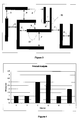
Figure 3 illustrates an exemplary selected design. However, the intervals and pitches
described herein are not limited to the selected design illustrated, and may include other
designs incorporating contact holes or designs incorporating lines and contact hole(s).
Intervals A, B, C, D, E, and F represent intervals having different numerical values. Any of
numerous methods may be utilized for performing an interval analysis (S100) to identify the
intervals A-F illustrated by Figure 3. The method may include manually inspecting the
selected design to identify each interval and to determine its value. Perhaps a simpler
technique would entail using a mask simulation program. Such an exemplary software
program is MASKWEAVER from ASML MaskTools that is capable of examining any
selected design and identifying and grouping like intervals.
In S102, the critical dense pitch is identified. For discussion purposes, assume interval
A corresponds to the critical dense pitch, i.e., the smallest combined interval and line width.
It follows that feature 30 corresponds to the critical feature.
In S104, lithographic apparatus settings may be iteratively adjusted until critical
feature 30 prints without the need for bias adjustment. The inventors have found that the NA
and sigma (sigma-outer and sigma-inner) may be adjusted to cause a critical feature to print
with or without bias adjustment. In other words, it is well known that any bias adjustment to
a critical feature may worsen the optical proximity affects, and is often difficult to perform.
Instead of adjusting the bias BA (i.e., altering feature geometry of feature 30) specified by an
OPC analysis, lithographic apparatus settings (i.e., exposure dose, NA, sigma-outer, and
sigma-inner) may be adjusted so that with or without bias adjustment feature 30 will print.
Because the amount of bias adjustments to a critical feature are often limited, depending on
the available space, adjusting lithographic apparatus settings is a simple way for causing the
critical feature to print.
Methods for adjusting NA and sigma are known to those of ordinary skill in lithograph
art. Perhaps the best way for adjusting these parameters may be accomplished by utilizing a
simulation software package such as Lithocruiser from ASML MaskTools that automatically
determines an optimal NA and sigma such that the critical feature will print. Of course, a
skilled lithographer could manually and iteratively adjust these parameters until a suitable
exposure dose is determined for printing the critical feature. In any event, optimal
lithographic apparatus parameters, such as NAoptimal, sigma-outeroptimal and sigma-inneroptimal,
may be determined such that bias adjustment BA is not required for feature 30 to print.
If more than one critical pitch is identified, the "most" critical feature is identified and
in most cases will corresponds to the smallest pitch, and optimal exposure dose parameters
may be determined. The other critical pitch(s) may be overcome by adjusting bias B.
In S106, scatter bar (SB) placement, SB width and bias is determined for each interval
in accordance with a guided estimation. This technique is well known to those of ordinary
skill in the art, and generally entails a lithographer selecting SB width and placement for a
given interval, and determining feature bias based on this interval. Simulation software, such
as Lithocruiser from ASML MaskTools may provide such a guided estimation.
The results of the guided estimation of S106 may be tabulated, as is shown by
exemplary Table 1. Accordingly, the size, placement, and length of each SB is shown in
tabulated form together with any bias adjustment.
| Interval | SB Placement | SB Width | SB Length | Bias |
| A | (x,y)A | WA | LA | BA |
| B | (x,y)B | WB | LB | BB |
| C | (x,y)C | WC | LC | BC |
| D | (x,y)D | WD | LD | BD |
| E | (x,y)E | WE | LE | BE |
| F | (x,y)F | WF | LF | BF |
In S108, an OPC analysis is performed on the selected design shown in Fig. 3 that
generates rules for intervals A - F, based on the guided estimation provided in S106.
Techniques for generating SB rules through an OPC analysis are known to those of ordinary
skill in the lithography art, and will require input of known lithographic apparatus parameters.
These may include the numerical aperture ("NA") of the lens of a lithographic apparatus and
sigma-outer and sigma-inner, which were discussed in connection to Fig. 1. Based on an
analysis of optical proximity affects, OPC rules may be generated for each interval which
specifies SB placement (x,y), SB Width (W), SB length (L), how many SB and any bias
adjustment (B) for each interval. Results of the OPC analysis may be tabulated, as shown by
Table 2. There is no bias adjustment required on the
critical feature 30, which corresponds to
interval A.
| Interval | SB Placement | SB Width | SB Length | SB Amount | Bias |
| A | (x,y)A | WA | LA | SB# | 0 |
| B | (x,y)B | WB | LB | SB# | BB |
| C | (x,y)C | WC | LC | SB# | BC |
| D | (x,y)D | WD | LD | SB# | 0 |
| E | (x,x)E | WE | LE | SB# | BE |
| F | (x,y)F | WF | LF | SB# | 0 |
Fig. 4 illustrates an exemplary histogram that may be generated for the selected design
of Fig. 3. The x-axis indicates intervals A - F and the y-axis indicates the frequency of each
interval A-F. Advantageously, this chart identifies the interval amounts in the design for
optimizing the SB placement (x,y), SB Width (W), SB length (L), how many SB and any bias
adjustment (B) for each interval. Without this analysis, a skilled lithographer may miss some
intervals that is critical for the design to get properly printed on wafer.
In S110, OPC adjustments are performed on the features other than the critical feature
30. Techniques for performing OPC adjustments are known to those of ordinary skill in the
art. A brief description will be given.
The inventors have found that the actual process window is substantially smaller,
when taking into consideration other features (including the critical feature) in the design.
Thus, the inventors have found that further enhancement of the lithographic apparatus
settings, and OPC treatment, will increase the process window for multiple features.
In S110, OPC adjustments are performed on features other than the critical feature,
and such a feature 32 is illustrated by Figure 3. These adjustments may be made by a cost
function analysis of feature 32.
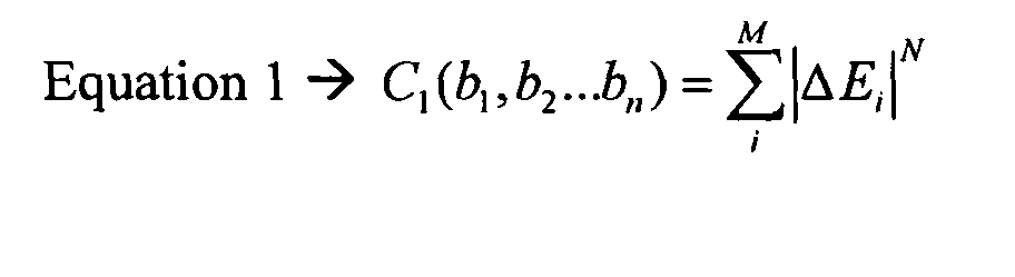
Equation 1 is a cost function that factors in the difference or deviation between a
predicted critical dimension (CD) and targeted CD for determining an optimal bias value.
Other cost functions may be utilized for determining an optimal bias value. However,
Equation 1 is useful for gradient based methods.
where,
b0, b1,...bn correspond to bias values ΔEi corresponds to the deviation between a targeted CD and a predicted CD, (0 ≤ i ≤ M) corresponds to the any number of samples, and N is a metric applied for solving for the an average case and worst case
behaviour of a chip.
Equation 1 may solved for a worst case behaviour (N is set at a high value).
Typically, designers choose N = 4, however, other values may be used. By solving for a
worst case behaviour, chip failure (e.g., caused by bridging) may be increasingly avoided.
According to Equation 1, an increasingly higher result (C1) corresponds to increasingly worst
case behaviour of a chip design. Therefore, equation 1 should be solved for a bias value (b0,
b1,...bn) in which C1 is a minimum.
Next, SBs are optimized.
Equation 2 represents a cost function for determining
optimal scattering bar placements.
where,
Like Equation 1, Equation 2 may solved for a worst case behaviour (N is set at a high
value). Typically, designers choose N = 4, however, other values may be used. By solving
for a worst case behaviour, chip failure may be increasingly avoided. According to Equation
2, an increasingly higher result (C2) corresponds to increasingly worse case behaviour of a
chip design. Therefore, equation 2 should be solved for distance values d 0 / 0, d 1 / 1,... d 1 / n and
d 2 / 0, d 2 / 1,... 2 / n in which C1 is a minimum.
Results of OPC adjustments of S10 are shown by Table 3. Assume that "[value] '"
represents an optimized value in accordance with S110.
| Interval | SB Placement | SB Width | SB Length | SB Amount | Bias |
| A | (x,y)A | WA | LA | SB# | 0 |
| B | (x,y)B | WB | LB | SB# | BB |
| C | (x,y)C' | WC' | LC' | SB# | BC' |
| D | (x,y)D | WD | LD | SB# | 0 |
| E | (x,y)E' | WE' | LE' | SB# | BE' |
| F | (x,y)F | WF | LF | SB# | 0 |
In S112, it is determined whether OPC adjustments are sufficient. One of ordinary
skill in the art can make this judgment. The sufficiency of the OPC adjustments in S110 may
be considered by examining any increase in the process window with the newly optimized
settings. Also, a lithographer may set a target process window for the entire design. For
example, a designer may set a target process window for multiple features to be at least 75%
area of the process window taking into consideration only the critical feature 30 or specify a
specific depth of focus (DOF) at certain value of exposure latitude (EL).
If it is determined that OPC treatment is not sufficient, lithographic apparatus settings
are further optimized based on the mask design which has been OPC-adjusted in step S110.
newly selected feature. S108 and S110 will be repeated until sufficient OPC treatment has
been accomplished. As opposed to optimizing lithographic apparatus settings for just the
critical feature, lithographic apparatus settings may be optimized for multiple features (i.e.,
the entire mask design).
EXAMPLE
Fig. 5 illustrates an exemplary target pattern.
Reference numeral 50 denotes a critical
feature (corresponding to the critical pitch of 320nm), and
reference numerals 52 and 54
denote other semi-isolated features other than the critical features. Critical features 50 were
identified corresponding to S100 and S102 (Fig. 2). The exemplary pattern of Fig. 5 was
illuminated using Quasar illumination having the parameters listed in Table 4.
| Quasar Illumination |
| Parameter | Setting |
| Wavelength | 0.248 |
| NA | 0.7 |
| Sigma Outer | 0.85 |
| Sigma Inner | 0.55 |
In S 106 (Fig. 2), lithographic apparatus settings may be optimized for the
critical
feature 50. Table 5 list the optimized parameters in accordance with S106, and corresponding
process window area.
| Optimized Quasar Illumination for CF 50 |
| Parameter | Setting |
| Wavelength | 0.248 |
| NA | 0.77 |
| Sigma Outer | 0.76 |
| Sigma Inner | 0.52 |
| Process Window Area | 1194.589573 |
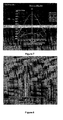
Fig. 7 illustrates the process window 70 for multiple cut lines 50, 52, 54, which are
illustrated by Fig. 5. When cut lines, in addition to cut line 50 are considered, the process
window 70 decreases in size as compared to the process window 60 of Fig. 6. In fact, the area
of process window 60 is dramatically reduced to 323.64918 (nm x mj/cm2).
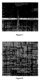
Figs. 8 and 9 are illustrative of the robustness of a lithographic apparatus that may
have variations in exposure settings and focus. Ideally, any variations should cause
corresponding variations within the critical dimension control specification. However, as
seen in Fig. 8, CD becomes bimodal in accordance with a variation of exposure settings and
focus and there are CD value fall outside of the specification. This is caused by operation
outside of the process window 70, also shown by Fig. 9. Further plotted on the graph of Fig.
9 is a plurality of CD values in accordance with a variation of exposure settings and focus.
Ideally, the CD values should remain within process window 70. It is readily apparent that
this is not the case. This is one of the problems that the disclosed concepts overcome by
mutually optimizing exposure settings and OPC adjustments for a plurality of features
including the critical feature 50. Figs. 8 and 9 are illustrative of insufficient OPC adjustments
determined in S112.
Recall that in S110, OPC adjustments are made on features other than the critical
feature 50. In this example, OPC adjustments would be made based on other features 52, 54.
Accordingly, the analysis of feedback loop comprising S108-S114 would cycle twice. Of
course, S110 may perform OPC adjustments on other features 52, 54.
Fig. 10 is a prime illustration of the process window for exposure settings and OPC
mutually optimized for a plurality of
features 50, 52, 54 including the
critical feature 50.
Table 6 lists the corresponding optimized exposure settings. By mutually optimizing
exposure settings and OPC adjustments in accordance with a plurality of features, the process
window area has been increased by almost 300% as compared to the process window (Fig. 7).
| Optimized Quasar Illumination for features 50-54 |
| Parameter | Setting |
| Wavelength | 0.248 |
| NA | 0.68 |
| Sigma Outer | 0.75 |
| Sigma Inner | 0.38 |
| Process Window Area | 941.654454 |
Figs. 11 and 12 are illustrative of the optimized robustness of a lithographic apparatus
that may have variations in exposure settings and focus variations. Again, any variations
should cause corresponding variations in the critical dimension. As seen in Fig. 11, CD
somewhat symmetrically changes with variations of exposure settings and focus, because
operation is within process window 100, also shown by Fig. 12. Further plotted on the graph
of Fig. 12 is a plurality of CD values in accordance with a variation of exposure settings and
focus. By mutually optimizing exposure settings and OPC for a plurality of features including
the critical feature 50, variations of CD fall within the process window that, in turn, increases
process margin.
Software may implement or aid in performing the disclosed concepts. Software
functionalities of a computer system involve programming, including executable code, may
be used to implement the above described optimization techniques. The software code is
executable by the general-purpose computer. In operation, the code and possibly the
associated data records are stored within a general-purpose computer platform. At other
times, however, the software may be stored at other locations and/or transported for loading
into the appropriate general-purpose computer systems. Hence, the embodiments discussed
above involve one or more software products in the form of one or more modules of code
carried by at least one machine-readable medium. Execution of such code by a processor of
the computer system enables the platform to implement the catalogue and/or software
downloading functions, in essentially the manner performed in the embodiments discussed
and illustrated herein.
As used herein, terms such as computer or machine "readable medium" refer to any
medium that participates in providing instructions to a processor for execution. Such a
medium may take many forms, including but not limited to, non-volatile media, volatile
media, and transmission media. Non-volatile media include, for example, optical or magnetic
disks, such as any of the storage devices in any computer(s) operating as one of the server
platform, discussed above. Volatile media include dynamic memory, such as main memory
of such a computer platform. Physical transmission media include coaxial cables; copper
wire and fibre optics, including the wires that comprise a bus within a computer system.
Carrier-wave transmission media can take the form of electric or electromagnetic signals, or
acoustic or light waves such as those generated during radio frequency (RF) and infrared (IR)
data communications. Common forms of computer-readable media therefore include, for
example: a floppy disk, a flexible disk, hard disk, magnetic tape, any other magnetic medium,
a CD-ROM, DVD, any other optical medium, less commonly used media such as punch
cards, paper tape, any other physical medium with patterns of holes, a RAM, a PROM, and
EPROM, a FLASH-EPROM, any other memory chip or cartridge, a carrier wave transporting
data or instructions, cables or links transporting such a carrier wave, or any other medium
from which a computer can read programming code and/or data. Many of these forms of
computer readable media may be involved in carrying one or more sequences of one or more
instructions to a processor for execution.
Although the present invention has been described and illustrated in detail, it is to be
clearly understood that the same is by way of illustration and example only and is not to be
taken by way of limitation, the scope of the present invention being limited only by the terms
of the appended claims.
This patent application, and any patent(s) issuing therefrom, claim priority from U.S.
provisional patent application number 60/483,102, filed on June 30, 2003, entitled "A method
and program product of simultaneous optimization for NA-Sigma exposure settings and
scattering bars OPC using a device layout," which is incorporated herein by reference in its
entirety.