EP1447850A2 - Elektronikteil-Gehäusungsstruktur und ihre Herstellungsmethode - Google Patents
Elektronikteil-Gehäusungsstruktur und ihre Herstellungsmethode Download PDFInfo
- Publication number
- EP1447850A2 EP1447850A2 EP04250677A EP04250677A EP1447850A2 EP 1447850 A2 EP1447850 A2 EP 1447850A2 EP 04250677 A EP04250677 A EP 04250677A EP 04250677 A EP04250677 A EP 04250677A EP 1447850 A2 EP1447850 A2 EP 1447850A2
- Authority
- EP
- European Patent Office
- Prior art keywords
- electronic parts
- insulating film
- wiring pattern
- opening portion
- connection terminal
- Prior art date
- Legal status (The legal status is an assumption and is not a legal conclusion. Google has not performed a legal analysis and makes no representation as to the accuracy of the status listed.)
- Withdrawn
Links
Images


Classifications
-
- H—ELECTRICITY
- H01—ELECTRIC ELEMENTS
- H01L—SEMICONDUCTOR DEVICES NOT COVERED BY CLASS H10
- H01L23/00—Details of semiconductor or other solid state devices
- H01L23/12—Mountings, e.g. non-detachable insulating substrates
-
- H—ELECTRICITY
- H01—ELECTRIC ELEMENTS
- H01L—SEMICONDUCTOR DEVICES NOT COVERED BY CLASS H10
- H01L23/00—Details of semiconductor or other solid state devices
- H01L23/52—Arrangements for conducting electric current within the device in operation from one component to another, i.e. interconnections, e.g. wires, lead frames
- H01L23/538—Arrangements for conducting electric current within the device in operation from one component to another, i.e. interconnections, e.g. wires, lead frames the interconnection structure between a plurality of semiconductor chips being formed on, or in, insulating substrates
- H01L23/5383—Multilayer substrates
-
- H—ELECTRICITY
- H01—ELECTRIC ELEMENTS
- H01L—SEMICONDUCTOR DEVICES NOT COVERED BY CLASS H10
- H01L21/00—Processes or apparatus adapted for the manufacture or treatment of semiconductor or solid state devices or of parts thereof
- H01L21/02—Manufacture or treatment of semiconductor devices or of parts thereof
- H01L21/04—Manufacture or treatment of semiconductor devices or of parts thereof the devices having at least one potential-jump barrier or surface barrier, e.g. PN junction, depletion layer or carrier concentration layer
- H01L21/50—Assembly of semiconductor devices using processes or apparatus not provided for in a single one of the subgroups H01L21/06 - H01L21/326, e.g. sealing of a cap to a base of a container
- H01L21/52—Mounting semiconductor bodies in containers
-
- H—ELECTRICITY
- H01—ELECTRIC ELEMENTS
- H01L—SEMICONDUCTOR DEVICES NOT COVERED BY CLASS H10
- H01L23/00—Details of semiconductor or other solid state devices
- H01L23/52—Arrangements for conducting electric current within the device in operation from one component to another, i.e. interconnections, e.g. wires, lead frames
- H01L23/538—Arrangements for conducting electric current within the device in operation from one component to another, i.e. interconnections, e.g. wires, lead frames the interconnection structure between a plurality of semiconductor chips being formed on, or in, insulating substrates
- H01L23/5389—Arrangements for conducting electric current within the device in operation from one component to another, i.e. interconnections, e.g. wires, lead frames the interconnection structure between a plurality of semiconductor chips being formed on, or in, insulating substrates the chips being integrally enclosed by the interconnect and support structures
-
- H—ELECTRICITY
- H01—ELECTRIC ELEMENTS
- H01L—SEMICONDUCTOR DEVICES NOT COVERED BY CLASS H10
- H01L24/00—Arrangements for connecting or disconnecting semiconductor or solid-state bodies; Methods or apparatus related thereto
- H01L24/01—Means for bonding being attached to, or being formed on, the surface to be connected, e.g. chip-to-package, die-attach, "first-level" interconnects; Manufacturing methods related thereto
- H01L24/18—High density interconnect [HDI] connectors; Manufacturing methods related thereto
- H01L24/23—Structure, shape, material or disposition of the high density interconnect connectors after the connecting process
- H01L24/24—Structure, shape, material or disposition of the high density interconnect connectors after the connecting process of an individual high density interconnect connector
-
- H—ELECTRICITY
- H01—ELECTRIC ELEMENTS
- H01L—SEMICONDUCTOR DEVICES NOT COVERED BY CLASS H10
- H01L24/00—Arrangements for connecting or disconnecting semiconductor or solid-state bodies; Methods or apparatus related thereto
- H01L24/80—Methods for connecting semiconductor or other solid state bodies using means for bonding being attached to, or being formed on, the surface to be connected
- H01L24/82—Methods for connecting semiconductor or other solid state bodies using means for bonding being attached to, or being formed on, the surface to be connected by forming build-up interconnects at chip-level, e.g. for high density interconnects [HDI]
-
- H—ELECTRICITY
- H01—ELECTRIC ELEMENTS
- H01L—SEMICONDUCTOR DEVICES NOT COVERED BY CLASS H10
- H01L24/00—Arrangements for connecting or disconnecting semiconductor or solid-state bodies; Methods or apparatus related thereto
- H01L24/91—Methods for connecting semiconductor or solid state bodies including different methods provided for in two or more of groups H01L24/80 - H01L24/90
- H01L24/92—Specific sequence of method steps
-
- H—ELECTRICITY
- H01—ELECTRIC ELEMENTS
- H01L—SEMICONDUCTOR DEVICES NOT COVERED BY CLASS H10
- H01L25/00—Assemblies consisting of a plurality of individual semiconductor or other solid state devices ; Multistep manufacturing processes thereof
- H01L25/03—Assemblies consisting of a plurality of individual semiconductor or other solid state devices ; Multistep manufacturing processes thereof all the devices being of a type provided for in the same subgroup of groups H01L27/00 - H01L33/00, or in a single subclass of H10K, H10N, e.g. assemblies of rectifier diodes
- H01L25/04—Assemblies consisting of a plurality of individual semiconductor or other solid state devices ; Multistep manufacturing processes thereof all the devices being of a type provided for in the same subgroup of groups H01L27/00 - H01L33/00, or in a single subclass of H10K, H10N, e.g. assemblies of rectifier diodes the devices not having separate containers
- H01L25/065—Assemblies consisting of a plurality of individual semiconductor or other solid state devices ; Multistep manufacturing processes thereof all the devices being of a type provided for in the same subgroup of groups H01L27/00 - H01L33/00, or in a single subclass of H10K, H10N, e.g. assemblies of rectifier diodes the devices not having separate containers the devices being of a type provided for in group H01L27/00
- H01L25/0657—Stacked arrangements of devices
-
- H—ELECTRICITY
- H05—ELECTRIC TECHNIQUES NOT OTHERWISE PROVIDED FOR
- H05K—PRINTED CIRCUITS; CASINGS OR CONSTRUCTIONAL DETAILS OF ELECTRIC APPARATUS; MANUFACTURE OF ASSEMBLAGES OF ELECTRICAL COMPONENTS
- H05K1/00—Printed circuits
- H05K1/18—Printed circuits structurally associated with non-printed electric components
- H05K1/182—Printed circuits structurally associated with non-printed electric components associated with components mounted in the printed circuit board, e.g. insert mounted components [IMC]
- H05K1/185—Components encapsulated in the insulating substrate of the printed circuit or incorporated in internal layers of a multilayer circuit
- H05K1/186—Components encapsulated in the insulating substrate of the printed circuit or incorporated in internal layers of a multilayer circuit manufactured by mounting on or connecting to patterned circuits before or during embedding
-
- H—ELECTRICITY
- H05—ELECTRIC TECHNIQUES NOT OTHERWISE PROVIDED FOR
- H05K—PRINTED CIRCUITS; CASINGS OR CONSTRUCTIONAL DETAILS OF ELECTRIC APPARATUS; MANUFACTURE OF ASSEMBLAGES OF ELECTRICAL COMPONENTS
- H05K3/00—Apparatus or processes for manufacturing printed circuits
- H05K3/30—Assembling printed circuits with electric components, e.g. with resistor
-
- H—ELECTRICITY
- H01—ELECTRIC ELEMENTS
- H01L—SEMICONDUCTOR DEVICES NOT COVERED BY CLASS H10
- H01L21/00—Processes or apparatus adapted for the manufacture or treatment of semiconductor or solid state devices or of parts thereof
- H01L21/02—Manufacture or treatment of semiconductor devices or of parts thereof
- H01L21/04—Manufacture or treatment of semiconductor devices or of parts thereof the devices having at least one potential-jump barrier or surface barrier, e.g. PN junction, depletion layer or carrier concentration layer
- H01L21/50—Assembly of semiconductor devices using processes or apparatus not provided for in a single one of the subgroups H01L21/06 - H01L21/326, e.g. sealing of a cap to a base of a container
- H01L21/56—Encapsulations, e.g. encapsulation layers, coatings
- H01L21/563—Encapsulation of active face of flip-chip device, e.g. underfilling or underencapsulation of flip-chip, encapsulation preform on chip or mounting substrate
-
- H—ELECTRICITY
- H01—ELECTRIC ELEMENTS
- H01L—SEMICONDUCTOR DEVICES NOT COVERED BY CLASS H10
- H01L21/00—Processes or apparatus adapted for the manufacture or treatment of semiconductor or solid state devices or of parts thereof
- H01L21/70—Manufacture or treatment of devices consisting of a plurality of solid state components formed in or on a common substrate or of parts thereof; Manufacture of integrated circuit devices or of parts thereof
- H01L21/71—Manufacture of specific parts of devices defined in group H01L21/70
- H01L21/768—Applying interconnections to be used for carrying current between separate components within a device comprising conductors and dielectrics
- H01L21/76898—Applying interconnections to be used for carrying current between separate components within a device comprising conductors and dielectrics formed through a semiconductor substrate
-
- H—ELECTRICITY
- H01—ELECTRIC ELEMENTS
- H01L—SEMICONDUCTOR DEVICES NOT COVERED BY CLASS H10
- H01L2224/00—Indexing scheme for arrangements for connecting or disconnecting semiconductor or solid-state bodies and methods related thereto as covered by H01L24/00
- H01L2224/01—Means for bonding being attached to, or being formed on, the surface to be connected, e.g. chip-to-package, die-attach, "first-level" interconnects; Manufacturing methods related thereto
- H01L2224/02—Bonding areas; Manufacturing methods related thereto
- H01L2224/023—Redistribution layers [RDL] for bonding areas
- H01L2224/0237—Disposition of the redistribution layers
- H01L2224/02372—Disposition of the redistribution layers connecting to a via connection in the semiconductor or solid-state body
-
- H—ELECTRICITY
- H01—ELECTRIC ELEMENTS
- H01L—SEMICONDUCTOR DEVICES NOT COVERED BY CLASS H10
- H01L2224/00—Indexing scheme for arrangements for connecting or disconnecting semiconductor or solid-state bodies and methods related thereto as covered by H01L24/00
- H01L2224/01—Means for bonding being attached to, or being formed on, the surface to be connected, e.g. chip-to-package, die-attach, "first-level" interconnects; Manufacturing methods related thereto
- H01L2224/02—Bonding areas; Manufacturing methods related thereto
- H01L2224/023—Redistribution layers [RDL] for bonding areas
- H01L2224/0237—Disposition of the redistribution layers
- H01L2224/02379—Fan-out arrangement
-
- H—ELECTRICITY
- H01—ELECTRIC ELEMENTS
- H01L—SEMICONDUCTOR DEVICES NOT COVERED BY CLASS H10
- H01L2224/00—Indexing scheme for arrangements for connecting or disconnecting semiconductor or solid-state bodies and methods related thereto as covered by H01L24/00
- H01L2224/01—Means for bonding being attached to, or being formed on, the surface to be connected, e.g. chip-to-package, die-attach, "first-level" interconnects; Manufacturing methods related thereto
- H01L2224/02—Bonding areas; Manufacturing methods related thereto
- H01L2224/04—Structure, shape, material or disposition of the bonding areas prior to the connecting process
- H01L2224/04105—Bonding areas formed on an encapsulation of the semiconductor or solid-state body, e.g. bonding areas on chip-scale packages
-
- H—ELECTRICITY
- H01—ELECTRIC ELEMENTS
- H01L—SEMICONDUCTOR DEVICES NOT COVERED BY CLASS H10
- H01L2224/00—Indexing scheme for arrangements for connecting or disconnecting semiconductor or solid-state bodies and methods related thereto as covered by H01L24/00
- H01L2224/01—Means for bonding being attached to, or being formed on, the surface to be connected, e.g. chip-to-package, die-attach, "first-level" interconnects; Manufacturing methods related thereto
- H01L2224/02—Bonding areas; Manufacturing methods related thereto
- H01L2224/04—Structure, shape, material or disposition of the bonding areas prior to the connecting process
- H01L2224/05—Structure, shape, material or disposition of the bonding areas prior to the connecting process of an individual bonding area
- H01L2224/05001—Internal layers
- H01L2224/0502—Disposition
- H01L2224/05022—Disposition the internal layer being at least partially embedded in the surface
-
- H—ELECTRICITY
- H01—ELECTRIC ELEMENTS
- H01L—SEMICONDUCTOR DEVICES NOT COVERED BY CLASS H10
- H01L2224/00—Indexing scheme for arrangements for connecting or disconnecting semiconductor or solid-state bodies and methods related thereto as covered by H01L24/00
- H01L2224/01—Means for bonding being attached to, or being formed on, the surface to be connected, e.g. chip-to-package, die-attach, "first-level" interconnects; Manufacturing methods related thereto
- H01L2224/02—Bonding areas; Manufacturing methods related thereto
- H01L2224/04—Structure, shape, material or disposition of the bonding areas prior to the connecting process
- H01L2224/05—Structure, shape, material or disposition of the bonding areas prior to the connecting process of an individual bonding area
- H01L2224/05001—Internal layers
- H01L2224/0502—Disposition
- H01L2224/05023—Disposition the whole internal layer protruding from the surface
-
- H—ELECTRICITY
- H01—ELECTRIC ELEMENTS
- H01L—SEMICONDUCTOR DEVICES NOT COVERED BY CLASS H10
- H01L2224/00—Indexing scheme for arrangements for connecting or disconnecting semiconductor or solid-state bodies and methods related thereto as covered by H01L24/00
- H01L2224/01—Means for bonding being attached to, or being formed on, the surface to be connected, e.g. chip-to-package, die-attach, "first-level" interconnects; Manufacturing methods related thereto
- H01L2224/02—Bonding areas; Manufacturing methods related thereto
- H01L2224/04—Structure, shape, material or disposition of the bonding areas prior to the connecting process
- H01L2224/05—Structure, shape, material or disposition of the bonding areas prior to the connecting process of an individual bonding area
- H01L2224/05001—Internal layers
- H01L2224/05075—Plural internal layers
- H01L2224/0508—Plural internal layers being stacked
-
- H—ELECTRICITY
- H01—ELECTRIC ELEMENTS
- H01L—SEMICONDUCTOR DEVICES NOT COVERED BY CLASS H10
- H01L2224/00—Indexing scheme for arrangements for connecting or disconnecting semiconductor or solid-state bodies and methods related thereto as covered by H01L24/00
- H01L2224/01—Means for bonding being attached to, or being formed on, the surface to be connected, e.g. chip-to-package, die-attach, "first-level" interconnects; Manufacturing methods related thereto
- H01L2224/02—Bonding areas; Manufacturing methods related thereto
- H01L2224/04—Structure, shape, material or disposition of the bonding areas prior to the connecting process
- H01L2224/05—Structure, shape, material or disposition of the bonding areas prior to the connecting process of an individual bonding area
- H01L2224/0554—External layer
- H01L2224/05541—Structure
- H01L2224/05548—Bonding area integrally formed with a redistribution layer on the semiconductor or solid-state body
-
- H—ELECTRICITY
- H01—ELECTRIC ELEMENTS
- H01L—SEMICONDUCTOR DEVICES NOT COVERED BY CLASS H10
- H01L2224/00—Indexing scheme for arrangements for connecting or disconnecting semiconductor or solid-state bodies and methods related thereto as covered by H01L24/00
- H01L2224/01—Means for bonding being attached to, or being formed on, the surface to be connected, e.g. chip-to-package, die-attach, "first-level" interconnects; Manufacturing methods related thereto
- H01L2224/02—Bonding areas; Manufacturing methods related thereto
- H01L2224/04—Structure, shape, material or disposition of the bonding areas prior to the connecting process
- H01L2224/05—Structure, shape, material or disposition of the bonding areas prior to the connecting process of an individual bonding area
- H01L2224/0554—External layer
- H01L2224/0556—Disposition
- H01L2224/05568—Disposition the whole external layer protruding from the surface
-
- H—ELECTRICITY
- H01—ELECTRIC ELEMENTS
- H01L—SEMICONDUCTOR DEVICES NOT COVERED BY CLASS H10
- H01L2224/00—Indexing scheme for arrangements for connecting or disconnecting semiconductor or solid-state bodies and methods related thereto as covered by H01L24/00
- H01L2224/01—Means for bonding being attached to, or being formed on, the surface to be connected, e.g. chip-to-package, die-attach, "first-level" interconnects; Manufacturing methods related thereto
- H01L2224/02—Bonding areas; Manufacturing methods related thereto
- H01L2224/04—Structure, shape, material or disposition of the bonding areas prior to the connecting process
- H01L2224/05—Structure, shape, material or disposition of the bonding areas prior to the connecting process of an individual bonding area
- H01L2224/0554—External layer
- H01L2224/05573—Single external layer
-
- H—ELECTRICITY
- H01—ELECTRIC ELEMENTS
- H01L—SEMICONDUCTOR DEVICES NOT COVERED BY CLASS H10
- H01L2224/00—Indexing scheme for arrangements for connecting or disconnecting semiconductor or solid-state bodies and methods related thereto as covered by H01L24/00
- H01L2224/01—Means for bonding being attached to, or being formed on, the surface to be connected, e.g. chip-to-package, die-attach, "first-level" interconnects; Manufacturing methods related thereto
- H01L2224/10—Bump connectors; Manufacturing methods related thereto
- H01L2224/12—Structure, shape, material or disposition of the bump connectors prior to the connecting process
- H01L2224/12105—Bump connectors formed on an encapsulation of the semiconductor or solid-state body, e.g. bumps on chip-scale packages
-
- H—ELECTRICITY
- H01—ELECTRIC ELEMENTS
- H01L—SEMICONDUCTOR DEVICES NOT COVERED BY CLASS H10
- H01L2224/00—Indexing scheme for arrangements for connecting or disconnecting semiconductor or solid-state bodies and methods related thereto as covered by H01L24/00
- H01L2224/01—Means for bonding being attached to, or being formed on, the surface to be connected, e.g. chip-to-package, die-attach, "first-level" interconnects; Manufacturing methods related thereto
- H01L2224/10—Bump connectors; Manufacturing methods related thereto
- H01L2224/12—Structure, shape, material or disposition of the bump connectors prior to the connecting process
- H01L2224/13—Structure, shape, material or disposition of the bump connectors prior to the connecting process of an individual bump connector
- H01L2224/13001—Core members of the bump connector
- H01L2224/13099—Material
- H01L2224/131—Material with a principal constituent of the material being a metal or a metalloid, e.g. boron [B], silicon [Si], germanium [Ge], arsenic [As], antimony [Sb], tellurium [Te] and polonium [Po], and alloys thereof
- H01L2224/13138—Material with a principal constituent of the material being a metal or a metalloid, e.g. boron [B], silicon [Si], germanium [Ge], arsenic [As], antimony [Sb], tellurium [Te] and polonium [Po], and alloys thereof the principal constituent melting at a temperature of greater than or equal to 950°C and less than 1550°C
- H01L2224/13144—Gold [Au] as principal constituent
-
- H—ELECTRICITY
- H01—ELECTRIC ELEMENTS
- H01L—SEMICONDUCTOR DEVICES NOT COVERED BY CLASS H10
- H01L2224/00—Indexing scheme for arrangements for connecting or disconnecting semiconductor or solid-state bodies and methods related thereto as covered by H01L24/00
- H01L2224/01—Means for bonding being attached to, or being formed on, the surface to be connected, e.g. chip-to-package, die-attach, "first-level" interconnects; Manufacturing methods related thereto
- H01L2224/10—Bump connectors; Manufacturing methods related thereto
- H01L2224/15—Structure, shape, material or disposition of the bump connectors after the connecting process
- H01L2224/16—Structure, shape, material or disposition of the bump connectors after the connecting process of an individual bump connector
- H01L2224/161—Disposition
- H01L2224/16135—Disposition the bump connector connecting between different semiconductor or solid-state bodies, i.e. chip-to-chip
- H01L2224/16145—Disposition the bump connector connecting between different semiconductor or solid-state bodies, i.e. chip-to-chip the bodies being stacked
- H01L2224/16146—Disposition the bump connector connecting between different semiconductor or solid-state bodies, i.e. chip-to-chip the bodies being stacked the bump connector connecting to a via connection in the semiconductor or solid-state body
-
- H—ELECTRICITY
- H01—ELECTRIC ELEMENTS
- H01L—SEMICONDUCTOR DEVICES NOT COVERED BY CLASS H10
- H01L2224/00—Indexing scheme for arrangements for connecting or disconnecting semiconductor or solid-state bodies and methods related thereto as covered by H01L24/00
- H01L2224/01—Means for bonding being attached to, or being formed on, the surface to be connected, e.g. chip-to-package, die-attach, "first-level" interconnects; Manufacturing methods related thereto
- H01L2224/10—Bump connectors; Manufacturing methods related thereto
- H01L2224/15—Structure, shape, material or disposition of the bump connectors after the connecting process
- H01L2224/16—Structure, shape, material or disposition of the bump connectors after the connecting process of an individual bump connector
- H01L2224/161—Disposition
- H01L2224/16151—Disposition the bump connector connecting between a semiconductor or solid-state body and an item not being a semiconductor or solid-state body, e.g. chip-to-substrate, chip-to-passive
- H01L2224/16221—Disposition the bump connector connecting between a semiconductor or solid-state body and an item not being a semiconductor or solid-state body, e.g. chip-to-substrate, chip-to-passive the body and the item being stacked
- H01L2224/16225—Disposition the bump connector connecting between a semiconductor or solid-state body and an item not being a semiconductor or solid-state body, e.g. chip-to-substrate, chip-to-passive the body and the item being stacked the item being non-metallic, e.g. insulating substrate with or without metallisation
- H01L2224/16238—Disposition the bump connector connecting between a semiconductor or solid-state body and an item not being a semiconductor or solid-state body, e.g. chip-to-substrate, chip-to-passive the body and the item being stacked the item being non-metallic, e.g. insulating substrate with or without metallisation the bump connector connecting to a bonding area protruding from the surface of the item
-
- H—ELECTRICITY
- H01—ELECTRIC ELEMENTS
- H01L—SEMICONDUCTOR DEVICES NOT COVERED BY CLASS H10
- H01L2224/00—Indexing scheme for arrangements for connecting or disconnecting semiconductor or solid-state bodies and methods related thereto as covered by H01L24/00
- H01L2224/01—Means for bonding being attached to, or being formed on, the surface to be connected, e.g. chip-to-package, die-attach, "first-level" interconnects; Manufacturing methods related thereto
- H01L2224/10—Bump connectors; Manufacturing methods related thereto
- H01L2224/15—Structure, shape, material or disposition of the bump connectors after the connecting process
- H01L2224/17—Structure, shape, material or disposition of the bump connectors after the connecting process of a plurality of bump connectors
- H01L2224/171—Disposition
- H01L2224/1718—Disposition being disposed on at least two different sides of the body, e.g. dual array
- H01L2224/17181—On opposite sides of the body
-
- H—ELECTRICITY
- H01—ELECTRIC ELEMENTS
- H01L—SEMICONDUCTOR DEVICES NOT COVERED BY CLASS H10
- H01L2224/00—Indexing scheme for arrangements for connecting or disconnecting semiconductor or solid-state bodies and methods related thereto as covered by H01L24/00
- H01L2224/01—Means for bonding being attached to, or being formed on, the surface to be connected, e.g. chip-to-package, die-attach, "first-level" interconnects; Manufacturing methods related thereto
- H01L2224/18—High density interconnect [HDI] connectors; Manufacturing methods related thereto
- H01L2224/23—Structure, shape, material or disposition of the high density interconnect connectors after the connecting process
- H01L2224/24—Structure, shape, material or disposition of the high density interconnect connectors after the connecting process of an individual high density interconnect connector
- H01L2224/241—Disposition
- H01L2224/24151—Connecting between a semiconductor or solid-state body and an item not being a semiconductor or solid-state body, e.g. chip-to-substrate, chip-to-passive
- H01L2224/24221—Connecting between a semiconductor or solid-state body and an item not being a semiconductor or solid-state body, e.g. chip-to-substrate, chip-to-passive the body and the item being stacked
- H01L2224/24225—Connecting between a semiconductor or solid-state body and an item not being a semiconductor or solid-state body, e.g. chip-to-substrate, chip-to-passive the body and the item being stacked the item being non-metallic, e.g. insulating substrate with or without metallisation
- H01L2224/24226—Connecting between a semiconductor or solid-state body and an item not being a semiconductor or solid-state body, e.g. chip-to-substrate, chip-to-passive the body and the item being stacked the item being non-metallic, e.g. insulating substrate with or without metallisation the HDI interconnect connecting to the same level of the item at which the semiconductor or solid-state body is mounted, e.g. the item being planar
-
- H—ELECTRICITY
- H01—ELECTRIC ELEMENTS
- H01L—SEMICONDUCTOR DEVICES NOT COVERED BY CLASS H10
- H01L2224/00—Indexing scheme for arrangements for connecting or disconnecting semiconductor or solid-state bodies and methods related thereto as covered by H01L24/00
- H01L2224/01—Means for bonding being attached to, or being formed on, the surface to be connected, e.g. chip-to-package, die-attach, "first-level" interconnects; Manufacturing methods related thereto
- H01L2224/26—Layer connectors, e.g. plate connectors, solder or adhesive layers; Manufacturing methods related thereto
- H01L2224/31—Structure, shape, material or disposition of the layer connectors after the connecting process
- H01L2224/32—Structure, shape, material or disposition of the layer connectors after the connecting process of an individual layer connector
- H01L2224/321—Disposition
- H01L2224/32151—Disposition the layer connector connecting between a semiconductor or solid-state body and an item not being a semiconductor or solid-state body, e.g. chip-to-substrate, chip-to-passive
- H01L2224/32221—Disposition the layer connector connecting between a semiconductor or solid-state body and an item not being a semiconductor or solid-state body, e.g. chip-to-substrate, chip-to-passive the body and the item being stacked
- H01L2224/32225—Disposition the layer connector connecting between a semiconductor or solid-state body and an item not being a semiconductor or solid-state body, e.g. chip-to-substrate, chip-to-passive the body and the item being stacked the item being non-metallic, e.g. insulating substrate with or without metallisation
-
- H—ELECTRICITY
- H01—ELECTRIC ELEMENTS
- H01L—SEMICONDUCTOR DEVICES NOT COVERED BY CLASS H10
- H01L2224/00—Indexing scheme for arrangements for connecting or disconnecting semiconductor or solid-state bodies and methods related thereto as covered by H01L24/00
- H01L2224/73—Means for bonding being of different types provided for in two or more of groups H01L2224/10, H01L2224/18, H01L2224/26, H01L2224/34, H01L2224/42, H01L2224/50, H01L2224/63, H01L2224/71
- H01L2224/732—Location after the connecting process
- H01L2224/73201—Location after the connecting process on the same surface
- H01L2224/73203—Bump and layer connectors
- H01L2224/73204—Bump and layer connectors the bump connector being embedded into the layer connector
-
- H—ELECTRICITY
- H01—ELECTRIC ELEMENTS
- H01L—SEMICONDUCTOR DEVICES NOT COVERED BY CLASS H10
- H01L2224/00—Indexing scheme for arrangements for connecting or disconnecting semiconductor or solid-state bodies and methods related thereto as covered by H01L24/00
- H01L2224/80—Methods for connecting semiconductor or other solid state bodies using means for bonding being attached to, or being formed on, the surface to be connected
- H01L2224/81—Methods for connecting semiconductor or other solid state bodies using means for bonding being attached to, or being formed on, the surface to be connected using a bump connector
- H01L2224/812—Applying energy for connecting
- H01L2224/81201—Compression bonding
- H01L2224/81205—Ultrasonic bonding
-
- H—ELECTRICITY
- H01—ELECTRIC ELEMENTS
- H01L—SEMICONDUCTOR DEVICES NOT COVERED BY CLASS H10
- H01L2224/00—Indexing scheme for arrangements for connecting or disconnecting semiconductor or solid-state bodies and methods related thereto as covered by H01L24/00
- H01L2224/80—Methods for connecting semiconductor or other solid state bodies using means for bonding being attached to, or being formed on, the surface to be connected
- H01L2224/81—Methods for connecting semiconductor or other solid state bodies using means for bonding being attached to, or being formed on, the surface to be connected using a bump connector
- H01L2224/812—Applying energy for connecting
- H01L2224/8121—Applying energy for connecting using a reflow oven
-
- H—ELECTRICITY
- H01—ELECTRIC ELEMENTS
- H01L—SEMICONDUCTOR DEVICES NOT COVERED BY CLASS H10
- H01L2224/00—Indexing scheme for arrangements for connecting or disconnecting semiconductor or solid-state bodies and methods related thereto as covered by H01L24/00
- H01L2224/80—Methods for connecting semiconductor or other solid state bodies using means for bonding being attached to, or being formed on, the surface to be connected
- H01L2224/81—Methods for connecting semiconductor or other solid state bodies using means for bonding being attached to, or being formed on, the surface to be connected using a bump connector
- H01L2224/818—Bonding techniques
- H01L2224/81801—Soldering or alloying
- H01L2224/81815—Reflow soldering
-
- H—ELECTRICITY
- H01—ELECTRIC ELEMENTS
- H01L—SEMICONDUCTOR DEVICES NOT COVERED BY CLASS H10
- H01L2224/00—Indexing scheme for arrangements for connecting or disconnecting semiconductor or solid-state bodies and methods related thereto as covered by H01L24/00
- H01L2224/80—Methods for connecting semiconductor or other solid state bodies using means for bonding being attached to, or being formed on, the surface to be connected
- H01L2224/82—Methods for connecting semiconductor or other solid state bodies using means for bonding being attached to, or being formed on, the surface to be connected by forming build-up interconnects at chip-level, e.g. for high density interconnects [HDI]
- H01L2224/82009—Pre-treatment of the connector or the bonding area
- H01L2224/8203—Reshaping, e.g. forming vias
- H01L2224/82035—Reshaping, e.g. forming vias by heating means
- H01L2224/82039—Reshaping, e.g. forming vias by heating means using a laser
-
- H—ELECTRICITY
- H01—ELECTRIC ELEMENTS
- H01L—SEMICONDUCTOR DEVICES NOT COVERED BY CLASS H10
- H01L2224/00—Indexing scheme for arrangements for connecting or disconnecting semiconductor or solid-state bodies and methods related thereto as covered by H01L24/00
- H01L2224/91—Methods for connecting semiconductor or solid state bodies including different methods provided for in two or more of groups H01L2224/80 - H01L2224/90
- H01L2224/92—Specific sequence of method steps
- H01L2224/9202—Forming additional connectors after the connecting process
-
- H—ELECTRICITY
- H01—ELECTRIC ELEMENTS
- H01L—SEMICONDUCTOR DEVICES NOT COVERED BY CLASS H10
- H01L2225/00—Details relating to assemblies covered by the group H01L25/00 but not provided for in its subgroups
- H01L2225/03—All the devices being of a type provided for in the same subgroup of groups H01L27/00 - H01L33/648 and H10K99/00
- H01L2225/04—All the devices being of a type provided for in the same subgroup of groups H01L27/00 - H01L33/648 and H10K99/00 the devices not having separate containers
- H01L2225/065—All the devices being of a type provided for in the same subgroup of groups H01L27/00 - H01L33/648 and H10K99/00 the devices not having separate containers the devices being of a type provided for in group H01L27/00
- H01L2225/06503—Stacked arrangements of devices
- H01L2225/06513—Bump or bump-like direct electrical connections between devices, e.g. flip-chip connection, solder bumps
-
- H—ELECTRICITY
- H01—ELECTRIC ELEMENTS
- H01L—SEMICONDUCTOR DEVICES NOT COVERED BY CLASS H10
- H01L2225/00—Details relating to assemblies covered by the group H01L25/00 but not provided for in its subgroups
- H01L2225/03—All the devices being of a type provided for in the same subgroup of groups H01L27/00 - H01L33/648 and H10K99/00
- H01L2225/04—All the devices being of a type provided for in the same subgroup of groups H01L27/00 - H01L33/648 and H10K99/00 the devices not having separate containers
- H01L2225/065—All the devices being of a type provided for in the same subgroup of groups H01L27/00 - H01L33/648 and H10K99/00 the devices not having separate containers the devices being of a type provided for in group H01L27/00
- H01L2225/06503—Stacked arrangements of devices
- H01L2225/06517—Bump or bump-like direct electrical connections from device to substrate
-
- H—ELECTRICITY
- H01—ELECTRIC ELEMENTS
- H01L—SEMICONDUCTOR DEVICES NOT COVERED BY CLASS H10
- H01L2225/00—Details relating to assemblies covered by the group H01L25/00 but not provided for in its subgroups
- H01L2225/03—All the devices being of a type provided for in the same subgroup of groups H01L27/00 - H01L33/648 and H10K99/00
- H01L2225/04—All the devices being of a type provided for in the same subgroup of groups H01L27/00 - H01L33/648 and H10K99/00 the devices not having separate containers
- H01L2225/065—All the devices being of a type provided for in the same subgroup of groups H01L27/00 - H01L33/648 and H10K99/00 the devices not having separate containers the devices being of a type provided for in group H01L27/00
- H01L2225/06503—Stacked arrangements of devices
- H01L2225/06524—Electrical connections formed on device or on substrate, e.g. a deposited or grown layer
-
- H—ELECTRICITY
- H01—ELECTRIC ELEMENTS
- H01L—SEMICONDUCTOR DEVICES NOT COVERED BY CLASS H10
- H01L2225/00—Details relating to assemblies covered by the group H01L25/00 but not provided for in its subgroups
- H01L2225/03—All the devices being of a type provided for in the same subgroup of groups H01L27/00 - H01L33/648 and H10K99/00
- H01L2225/04—All the devices being of a type provided for in the same subgroup of groups H01L27/00 - H01L33/648 and H10K99/00 the devices not having separate containers
- H01L2225/065—All the devices being of a type provided for in the same subgroup of groups H01L27/00 - H01L33/648 and H10K99/00 the devices not having separate containers the devices being of a type provided for in group H01L27/00
- H01L2225/06503—Stacked arrangements of devices
- H01L2225/06541—Conductive via connections through the device, e.g. vertical interconnects, through silicon via [TSV]
-
- H—ELECTRICITY
- H01—ELECTRIC ELEMENTS
- H01L—SEMICONDUCTOR DEVICES NOT COVERED BY CLASS H10
- H01L2225/00—Details relating to assemblies covered by the group H01L25/00 but not provided for in its subgroups
- H01L2225/03—All the devices being of a type provided for in the same subgroup of groups H01L27/00 - H01L33/648 and H10K99/00
- H01L2225/04—All the devices being of a type provided for in the same subgroup of groups H01L27/00 - H01L33/648 and H10K99/00 the devices not having separate containers
- H01L2225/065—All the devices being of a type provided for in the same subgroup of groups H01L27/00 - H01L33/648 and H10K99/00 the devices not having separate containers the devices being of a type provided for in group H01L27/00
- H01L2225/06503—Stacked arrangements of devices
- H01L2225/06572—Auxiliary carrier between devices, the carrier having an electrical connection structure
-
- H—ELECTRICITY
- H01—ELECTRIC ELEMENTS
- H01L—SEMICONDUCTOR DEVICES NOT COVERED BY CLASS H10
- H01L24/00—Arrangements for connecting or disconnecting semiconductor or solid-state bodies; Methods or apparatus related thereto
- H01L24/01—Means for bonding being attached to, or being formed on, the surface to be connected, e.g. chip-to-package, die-attach, "first-level" interconnects; Manufacturing methods related thereto
- H01L24/02—Bonding areas ; Manufacturing methods related thereto
- H01L24/03—Manufacturing methods
-
- H—ELECTRICITY
- H01—ELECTRIC ELEMENTS
- H01L—SEMICONDUCTOR DEVICES NOT COVERED BY CLASS H10
- H01L24/00—Arrangements for connecting or disconnecting semiconductor or solid-state bodies; Methods or apparatus related thereto
- H01L24/01—Means for bonding being attached to, or being formed on, the surface to be connected, e.g. chip-to-package, die-attach, "first-level" interconnects; Manufacturing methods related thereto
- H01L24/02—Bonding areas ; Manufacturing methods related thereto
- H01L24/04—Structure, shape, material or disposition of the bonding areas prior to the connecting process
- H01L24/05—Structure, shape, material or disposition of the bonding areas prior to the connecting process of an individual bonding area
-
- H—ELECTRICITY
- H01—ELECTRIC ELEMENTS
- H01L—SEMICONDUCTOR DEVICES NOT COVERED BY CLASS H10
- H01L24/00—Arrangements for connecting or disconnecting semiconductor or solid-state bodies; Methods or apparatus related thereto
- H01L24/80—Methods for connecting semiconductor or other solid state bodies using means for bonding being attached to, or being formed on, the surface to be connected
- H01L24/81—Methods for connecting semiconductor or other solid state bodies using means for bonding being attached to, or being formed on, the surface to be connected using a bump connector
-
- H—ELECTRICITY
- H01—ELECTRIC ELEMENTS
- H01L—SEMICONDUCTOR DEVICES NOT COVERED BY CLASS H10
- H01L2924/00—Indexing scheme for arrangements or methods for connecting or disconnecting semiconductor or solid-state bodies as covered by H01L24/00
- H01L2924/0001—Technical content checked by a classifier
- H01L2924/00011—Not relevant to the scope of the group, the symbol of which is combined with the symbol of this group
-
- H—ELECTRICITY
- H01—ELECTRIC ELEMENTS
- H01L—SEMICONDUCTOR DEVICES NOT COVERED BY CLASS H10
- H01L2924/00—Indexing scheme for arrangements or methods for connecting or disconnecting semiconductor or solid-state bodies as covered by H01L24/00
- H01L2924/0001—Technical content checked by a classifier
- H01L2924/00014—Technical content checked by a classifier the subject-matter covered by the group, the symbol of which is combined with the symbol of this group, being disclosed without further technical details
-
- H—ELECTRICITY
- H01—ELECTRIC ELEMENTS
- H01L—SEMICONDUCTOR DEVICES NOT COVERED BY CLASS H10
- H01L2924/00—Indexing scheme for arrangements or methods for connecting or disconnecting semiconductor or solid-state bodies as covered by H01L24/00
- H01L2924/01—Chemical elements
- H01L2924/01004—Beryllium [Be]
-
- H—ELECTRICITY
- H01—ELECTRIC ELEMENTS
- H01L—SEMICONDUCTOR DEVICES NOT COVERED BY CLASS H10
- H01L2924/00—Indexing scheme for arrangements or methods for connecting or disconnecting semiconductor or solid-state bodies as covered by H01L24/00
- H01L2924/01—Chemical elements
- H01L2924/01005—Boron [B]
-
- H—ELECTRICITY
- H01—ELECTRIC ELEMENTS
- H01L—SEMICONDUCTOR DEVICES NOT COVERED BY CLASS H10
- H01L2924/00—Indexing scheme for arrangements or methods for connecting or disconnecting semiconductor or solid-state bodies as covered by H01L24/00
- H01L2924/01—Chemical elements
- H01L2924/01006—Carbon [C]
-
- H—ELECTRICITY
- H01—ELECTRIC ELEMENTS
- H01L—SEMICONDUCTOR DEVICES NOT COVERED BY CLASS H10
- H01L2924/00—Indexing scheme for arrangements or methods for connecting or disconnecting semiconductor or solid-state bodies as covered by H01L24/00
- H01L2924/01—Chemical elements
- H01L2924/01015—Phosphorus [P]
-
- H—ELECTRICITY
- H01—ELECTRIC ELEMENTS
- H01L—SEMICONDUCTOR DEVICES NOT COVERED BY CLASS H10
- H01L2924/00—Indexing scheme for arrangements or methods for connecting or disconnecting semiconductor or solid-state bodies as covered by H01L24/00
- H01L2924/01—Chemical elements
- H01L2924/01027—Cobalt [Co]
-
- H—ELECTRICITY
- H01—ELECTRIC ELEMENTS
- H01L—SEMICONDUCTOR DEVICES NOT COVERED BY CLASS H10
- H01L2924/00—Indexing scheme for arrangements or methods for connecting or disconnecting semiconductor or solid-state bodies as covered by H01L24/00
- H01L2924/01—Chemical elements
- H01L2924/01029—Copper [Cu]
-
- H—ELECTRICITY
- H01—ELECTRIC ELEMENTS
- H01L—SEMICONDUCTOR DEVICES NOT COVERED BY CLASS H10
- H01L2924/00—Indexing scheme for arrangements or methods for connecting or disconnecting semiconductor or solid-state bodies as covered by H01L24/00
- H01L2924/01—Chemical elements
- H01L2924/01033—Arsenic [As]
-
- H—ELECTRICITY
- H01—ELECTRIC ELEMENTS
- H01L—SEMICONDUCTOR DEVICES NOT COVERED BY CLASS H10
- H01L2924/00—Indexing scheme for arrangements or methods for connecting or disconnecting semiconductor or solid-state bodies as covered by H01L24/00
- H01L2924/01—Chemical elements
- H01L2924/01047—Silver [Ag]
-
- H—ELECTRICITY
- H01—ELECTRIC ELEMENTS
- H01L—SEMICONDUCTOR DEVICES NOT COVERED BY CLASS H10
- H01L2924/00—Indexing scheme for arrangements or methods for connecting or disconnecting semiconductor or solid-state bodies as covered by H01L24/00
- H01L2924/01—Chemical elements
- H01L2924/01057—Lanthanum [La]
-
- H—ELECTRICITY
- H01—ELECTRIC ELEMENTS
- H01L—SEMICONDUCTOR DEVICES NOT COVERED BY CLASS H10
- H01L2924/00—Indexing scheme for arrangements or methods for connecting or disconnecting semiconductor or solid-state bodies as covered by H01L24/00
- H01L2924/01—Chemical elements
- H01L2924/01075—Rhenium [Re]
-
- H—ELECTRICITY
- H01—ELECTRIC ELEMENTS
- H01L—SEMICONDUCTOR DEVICES NOT COVERED BY CLASS H10
- H01L2924/00—Indexing scheme for arrangements or methods for connecting or disconnecting semiconductor or solid-state bodies as covered by H01L24/00
- H01L2924/01—Chemical elements
- H01L2924/01078—Platinum [Pt]
-
- H—ELECTRICITY
- H01—ELECTRIC ELEMENTS
- H01L—SEMICONDUCTOR DEVICES NOT COVERED BY CLASS H10
- H01L2924/00—Indexing scheme for arrangements or methods for connecting or disconnecting semiconductor or solid-state bodies as covered by H01L24/00
- H01L2924/01—Chemical elements
- H01L2924/01079—Gold [Au]
-
- H—ELECTRICITY
- H01—ELECTRIC ELEMENTS
- H01L—SEMICONDUCTOR DEVICES NOT COVERED BY CLASS H10
- H01L2924/00—Indexing scheme for arrangements or methods for connecting or disconnecting semiconductor or solid-state bodies as covered by H01L24/00
- H01L2924/013—Alloys
- H01L2924/014—Solder alloys
-
- H—ELECTRICITY
- H01—ELECTRIC ELEMENTS
- H01L—SEMICONDUCTOR DEVICES NOT COVERED BY CLASS H10
- H01L2924/00—Indexing scheme for arrangements or methods for connecting or disconnecting semiconductor or solid-state bodies as covered by H01L24/00
- H01L2924/10—Details of semiconductor or other solid state devices to be connected
- H01L2924/11—Device type
- H01L2924/12—Passive devices, e.g. 2 terminal devices
- H01L2924/1204—Optical Diode
- H01L2924/12042—LASER
-
- H—ELECTRICITY
- H01—ELECTRIC ELEMENTS
- H01L—SEMICONDUCTOR DEVICES NOT COVERED BY CLASS H10
- H01L2924/00—Indexing scheme for arrangements or methods for connecting or disconnecting semiconductor or solid-state bodies as covered by H01L24/00
- H01L2924/19—Details of hybrid assemblies other than the semiconductor or other solid state devices to be connected
- H01L2924/1901—Structure
- H01L2924/1904—Component type
- H01L2924/19041—Component type being a capacitor
-
- H—ELECTRICITY
- H01—ELECTRIC ELEMENTS
- H01L—SEMICONDUCTOR DEVICES NOT COVERED BY CLASS H10
- H01L2924/00—Indexing scheme for arrangements or methods for connecting or disconnecting semiconductor or solid-state bodies as covered by H01L24/00
- H01L2924/19—Details of hybrid assemblies other than the semiconductor or other solid state devices to be connected
- H01L2924/1901—Structure
- H01L2924/1904—Component type
- H01L2924/19043—Component type being a resistor
-
- H—ELECTRICITY
- H01—ELECTRIC ELEMENTS
- H01L—SEMICONDUCTOR DEVICES NOT COVERED BY CLASS H10
- H01L2924/00—Indexing scheme for arrangements or methods for connecting or disconnecting semiconductor or solid-state bodies as covered by H01L24/00
- H01L2924/30—Technical effects
- H01L2924/301—Electrical effects
- H01L2924/30105—Capacitance
-
- H—ELECTRICITY
- H05—ELECTRIC TECHNIQUES NOT OTHERWISE PROVIDED FOR
- H05K—PRINTED CIRCUITS; CASINGS OR CONSTRUCTIONAL DETAILS OF ELECTRIC APPARATUS; MANUFACTURE OF ASSEMBLAGES OF ELECTRICAL COMPONENTS
- H05K2201/00—Indexing scheme relating to printed circuits covered by H05K1/00
- H05K2201/01—Dielectrics
- H05K2201/0183—Dielectric layers
- H05K2201/0195—Dielectric or adhesive layers comprising a plurality of layers, e.g. in a multilayer structure
-
- H—ELECTRICITY
- H05—ELECTRIC TECHNIQUES NOT OTHERWISE PROVIDED FOR
- H05K—PRINTED CIRCUITS; CASINGS OR CONSTRUCTIONAL DETAILS OF ELECTRIC APPARATUS; MANUFACTURE OF ASSEMBLAGES OF ELECTRICAL COMPONENTS
- H05K2201/00—Indexing scheme relating to printed circuits covered by H05K1/00
- H05K2201/10—Details of components or other objects attached to or integrated in a printed circuit board
- H05K2201/10613—Details of electrical connections of non-printed components, e.g. special leads
- H05K2201/10621—Components characterised by their electrical contacts
- H05K2201/10636—Leadless chip, e.g. chip capacitor or resistor
-
- H—ELECTRICITY
- H05—ELECTRIC TECHNIQUES NOT OTHERWISE PROVIDED FOR
- H05K—PRINTED CIRCUITS; CASINGS OR CONSTRUCTIONAL DETAILS OF ELECTRIC APPARATUS; MANUFACTURE OF ASSEMBLAGES OF ELECTRICAL COMPONENTS
- H05K2201/00—Indexing scheme relating to printed circuits covered by H05K1/00
- H05K2201/10—Details of components or other objects attached to or integrated in a printed circuit board
- H05K2201/10613—Details of electrical connections of non-printed components, e.g. special leads
- H05K2201/10621—Components characterised by their electrical contacts
- H05K2201/10674—Flip chip
-
- H—ELECTRICITY
- H05—ELECTRIC TECHNIQUES NOT OTHERWISE PROVIDED FOR
- H05K—PRINTED CIRCUITS; CASINGS OR CONSTRUCTIONAL DETAILS OF ELECTRIC APPARATUS; MANUFACTURE OF ASSEMBLAGES OF ELECTRICAL COMPONENTS
- H05K3/00—Apparatus or processes for manufacturing printed circuits
- H05K3/46—Manufacturing multilayer circuits
- H05K3/4644—Manufacturing multilayer circuits by building the multilayer layer by layer, i.e. build-up multilayer circuits
-
- Y—GENERAL TAGGING OF NEW TECHNOLOGICAL DEVELOPMENTS; GENERAL TAGGING OF CROSS-SECTIONAL TECHNOLOGIES SPANNING OVER SEVERAL SECTIONS OF THE IPC; TECHNICAL SUBJECTS COVERED BY FORMER USPC CROSS-REFERENCE ART COLLECTIONS [XRACs] AND DIGESTS
- Y02—TECHNOLOGIES OR APPLICATIONS FOR MITIGATION OR ADAPTATION AGAINST CLIMATE CHANGE
- Y02P—CLIMATE CHANGE MITIGATION TECHNOLOGIES IN THE PRODUCTION OR PROCESSING OF GOODS
- Y02P70/00—Climate change mitigation technologies in the production process for final industrial or consumer products
- Y02P70/50—Manufacturing or production processes characterised by the final manufactured product
Definitions
- the present invention relates to an electronic parts packaging structure and a method of manufacturing the same. More specifically, the present invention relates to an electronic parts packaging structure in which a semiconductor chip or the like is mounted on a wiring substrate in the state where the semiconductor chip or the like is buried in an insulating film, and to a method of manufacturing the same.
- Patent Literature 1 Japanese Unexamined Patent Publication No. 2001-177045
- Patent Literature 2 Japanese Unexamined Patent Publication No. 2000-323645 discloses a semiconductor device having a structure as follows: a plurality of semiconductor chips are three-dimensionally mounted on a wiring substrate in the state where the semiconductor chips are buried in insulating films, and the plurality of semiconductor chips are mutually connected using multilayered wiring patterns or the like formed with the insulating films interposed therebetween.
- Patent Literatures 1 and 2 there is no consideration for the fact that an interlayer insulating film is formed in the state where steps are generated due to the thickness of a semiconductor chip when the interlayer insulating film is formed on the mounted semiconductor chip.
- steps are also generated in the wiring patterns formed on the interlayer insulating film, reliability of bonding may be lowered when a semiconductor chip is flip-chip bonded to the wiring patterns.
- an electronic parts packaging structure having a structure in which an electronic parts is buried in an insulating film on a wiring substrate, wherein steps due to the thickness of the electronic parts may be eliminated to be planarized, and to provide a method of manufacturing the same.
- an electronic parts packaging structure including a wiring substrate having a wiring pattern, a first insulating film which is formed on the wiring substrate and which has an opening portion in a packaging area where an electronic parts is mounted, the electronic parts having a connection terminal flip-chip mounted on the wiring pattern of the opening portion of the first insulating film, a second insulating film for covering the electronic parts, a via hole formed in a predetermined portion of the first and second insulating films on the wiring pattern, and an upper wiring pattern formed on the second insulating film and connected to the wiring pattern through the via hole.
- the first insulating film (a resin film) having the opening portion in the packaging area is formed on the wiring substrate, and the connection terminal of the electronic parts (thinned semiconductor chip or the like) is flip-chip mounted on the wiring pattern in the opening portion.
- the second insulating film for covering the electronic parts is formed, and the via hole is formed in the first and second insulating films on the wiring pattern.
- the upper wiring pattern connected to the wiring pattern through the via hole is formed on the second insulating film.
- the first insulating film is formed so as to surround the electronic parts. Therefore, this embodiment of the present invention has a structure in which steps due to the thickness of the electronic parts are eliminated with the first insulating film. Accordingly, the second insulating film for covering the electronic parts is formed in the state where the upper surface of the second insulating film is planar, without being affected by the thickness of the electronic parts.
- the upper wiring pattern is stably formed with high precision.
- the electronic parts is flip-chip mounted on the wiring pattern in the state where the electronic parts is buried in a planar insulating film, and the upper wiring pattern for three-dimensionally multilayering a plurality of electronic parts is formed on the second insulating film without the occurrence of any trouble. Furthermore, in the case where an upper electronic parts is flip-chip mounted on the upper wiring pattern, a connection portion of the upper wiring pattern is placed at substantially the same height. Accordingly, the upper electronic parts is bonded thereto with high reliability.
- the second insulating film may be omitted by providing a protection film on the backside of the electronic parts.
- the upper wiring pattern is formed on the first insulating film and the protection film.
- the following structure may be adopted: without forming a via hole in the insulating film on the wiring pattern, a via hole penetrating the electronic parts is formed in a predetermined portion of the electronic parts on the connection terminal, and the upper wiring pattern is connected to the connection terminal through the via hole of the electronic parts.
- connection terminal of the electronic parts is made of gold
- a gold film is formed on a surface of the wiring pattern in the opening portion of the insulating film
- the connection terminal of the electronic parts is flip-chip mounted on the wiring pattern by gold-gold bonding.
- the first insulating film for eliminating steps due to the thickness of the electronic parts is also used as a mask layer for selectively forming the gold film on the wiring pattern (copper wiring or the like) in the opening portion (packaging area) of the first resin film. This makes it possible to easily flip-chip mount the electronic parts having the connection terminal made of gold on the wiring pattern by gold-gold bonding which provides high reliability of bonding.
- an electronic parts packaging structure including a wiring substrate having a wiring pattern, a first insulating film formed on the wiring substrate which has an opening portion in a packaging area where an electronic parts is mounted, the electronic parts mounted in the packaging area of the opening portion of the first insulating film in a state where a connection portion is directed upward, a second insulating film for covering the electronic parts, via holes respectively formed in predetermined portions of the insulating films on the connection terminal and the wiring pattern, and upper wiring patterns which are formed on the second insulating film and which are respectively connected to the connection terminal and the wiring pattern through the via holes.
- the first insulating film having the opening portion in the packaging area is formed on the wiring substrate, and the electronic parts is mounted in the opening portion in the state where the connection terminal is directed upward.
- the via holes are formed in predetermined portions in the second insulating film on the connection terminal and the' wiring pattern, respectively.
- the upper wiring patterns respectively connected to the connection terminal and the wiring pattern through the via holes are stably formed on the second insulating film with high precision.
- the second insulating film for covering the electronic parts may be omitted by use of an electronic parts provided with a passivation film having an opening portion for exposing the connection terminal, on the element formation surface.
- the upper wiring patterns are formed on the insulating film and the passivation film.
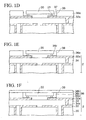
- FIGS. 1A to 1N are sectional views showing a method of manufacturing an electronic parts packaging structure of a first embodiment of the present invention in order.
- a base substrate 30 for manufacturing a build-up printed circuit board is prepared.
- the base substrate 30 is made of insulative material such as resin.
- Through-holes 30a are provided in the base substrate 30, and through-hole plating layers 30b connected to first wiring patterns 32 on the base substrate 30 are formed on the inner surfaces of the through-holes 30a. Openings of the through-holes 30a are filled with a resin body 30c.
- first interlayer insulating film 34 made of resin or the like, which covers the first wiring patterns 32 is formed. Then, predetermined portions of the first interlayer insulating film 34 on the first wiring patterns 32 are etched by a laser, RIE, or the like, thereby forming first via holes 34x having depths reaching the first wiring patterns 32.
- second wiring patterns 32a connected to the first wiring patterns 32 through the first via holes 34x are formed on the first interlayer insulating film 34.
- the second wiring patterns 32a are made of Cu wirings or the like and formed by a similar method to that of forming third wiring patterns to be described later.
- a wiring substrate 2, on which a semiconductor chip is mounted is obtained.
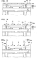
- first insulating film 36a epoxy series resin, polyimide series resin, novolac series resin, acrylic series resin, or the like is used.
- Methods of forming the first insulating film 36a include a method of patterning a photosensitive resin film by photolithography. Alternatively, a method may be employed in which a film-like resin layer is laminated to be formed or a resin film is formed by spin coating or printing, and then the resin film is etched by a laser or RIE, thereby forming the opening portion. Moreover, a method may be adopted in which a desired portion of a film-like resin layer is stamped out with a die to form the opening portion, and the resin film is attached. Furthermore, a resin film may be patterned into a shape having the opening portion by screen printing.
- Such a resin film is heat-treated at a temperature of 130 to 200 °C to be cured, thereby obtaining the first resin film 36a.
- One feature of the present embodiment is that when a structure in which a semiconductor chip is mounted in the state of being buried in an insulating film is formed, steps due to the thickness of the semiconductor chip are easily eliminated. Accordingly, in the present embodiment, the first insulating film 36a having the opening portion 39 in the packaging area A is formed to a thickness corresponding to the thickness of a semiconductor chip, and the semiconductor chip is mounted in the opening portion 39. Thus, steps due to the thickness of the semiconductor chip are easily eliminated with the first insulating film 36a.
- the thickness of the first insulating film 36a is appropriately adjusted in accordance with the thicknesses of various kinds of semiconductor chips.
- the thickness of the first insulating film 36a is set to a thickness equivalent to that of such a semiconductor chip.
- the opening portion 39 of the first insulating film 36a is preferably formed so as to surround a semiconductor chip to be mounted later.
- gold (Au) films 37 having thicknesses of 0.1 to 1 ⁇ m are selectively formed by electroless plating on the second wiring patterns (Cu wirings) 32a exposed in the opening portion 39 of the first insulating film 36a.
- the first insulating film 36a is made of a cured resin film, the first insulating film 36a is resistant to plating chemical for electroless plating.
- the Au films 37 may be formed after nickel (Ni) films have been formed as barrier films on the second wiring patterns (Cu wirings) 32a by electroless plating.
- the first insulating film 36a also functions as a mask layer for selectively forming the Au films 37 on connection portions B of the second wiring patterns (Cu wirings) 32a in the packaging area A.
- a semiconductor chip 20 having Au bumps 21 as shown in FIG. 1D is prepared.
- the semiconductor chip 20 is obtained as follows: a semiconductor wafer (not shown), which has elements, such as transistors, and connection pads on an element formation surface, is thinned to a thickness of approximately 150 ⁇ m (preferably, approximately 50 ⁇ m or less by grinding the backside of the semiconductor wafer, and then the semiconductor wafer is diced to be divided into individual pieces.
- the Au bumps 21 of the semiconductor chip 20 are formed on the connection pads before or after the semiconductor wafer is diced.
- connection pads and the bumps 21 of the semiconductor chip 20 are examples of connection terminals.
- the semiconductor chip 20 picked up with an ultrasonic tool is placed on the Au films 37 of the connection portions B of the second wiring patterns 32a in the state where the Au bumps 21 of the semiconductor chip 20 are directed downward, and ultrasonic vibration is applied horizontally while pressure is applied downward.
- the Au bumps 21 of the semiconductor chip 20 and the Au films 37 of the second wiring patterns 32a are bonded together.
- the semiconductor chip 20 is mounted on the second wiring patterns 32a by ultrasonic flip-chip bonding.
- the size of the opening portion 39 of the first insulating film 36a is preferably adjusted in accordance with the size of the semiconductor chip 20 so that a gap of 0.5 to 2 mm (preferably, approximately 1 mm) may be left between the side surfaces of the semiconductor chip 20 and those of the opening portion 39.
- the backside of the semiconductor chip 20 and the upper surface of the first insulating film 36a are at almost the same height, and steps due to the thickness of the semiconductor chip 20 are eliminated, because the first insulating film 36a is formed in an area except the packaging area A to almost the same thickness as that of the semiconductor chip 20 as previously described.
- the height of the backside of the semiconductor chip 20 and that of the upper surface of the first insulating film 36a may be different from each other to a degree in which troubles do not occur in subsequent steps.
- connection portions B of the second wiring patterns 32a can be bonded by Au-Au bonding at low cost.
- eliminating steps due to the thickness of the semiconductor chip 20 by forming the first insulating film 36a having the opening portion 39 in the packaging area A is very convenient for the case where the Au bumps 21 of the semiconductor chip 20 and the second wiring patterns 32a are bonded by Au-Au bonding, because the Au films 37 can be selectively formed on the connection portions B of the second wiring patterns 32a.
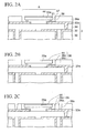
- Cu wirings having no Au films formed on the surfaces thereof is used as the second wiring patterns 32a,and the semiconductor chip 20 having solder bumps may be flip-chip bonded to the Cu wirings of the second wiring patterns 32a.
- the semiconductor chip 20 having solder bumps may be flip-chip bonded to the second wiring patterns 32a having the Au films 37 formed on the surfaces thereof as previously described.
- other various kinds of flip-chip mounting may be employed.
- a resin film having an opening portion in an area corresponding to the packaging area A may be attached after the semiconductor chip 20 is flip-chip mounted on the second wiring patterns 32a in the packaging area A.
- the opening portion of the resin film is stamped out with a die to be formed in advance.
- resin material is injected from the gap between the semiconductor chip 20 and the opening portion 39 of the first insulating film 36a, thereby filling the gap between the semiconductor chip 20 and the wiring substrate 2 and the gap between the semiconductor chip 20 and the side surfaces of the opening portion 39 of the first insulating film 36a with the resin material. Thereafter, the resin material is cured by heat treatment to become underfill resin 36c (filling insulating film).
- underfill resin 36c filling insulating film
- the underfill resin 36c may be formed as follows: insulating resin (NCF or NCP) is previously coated in a predetermined area including the packaging area A before the semiconductor chip 20 is flip-chip mounted, flip-chip bonding is performed in the state where this resin is interposed therebetween, and then the resin is cured by heat treatment to become the underfill resin 36c.
- insulating resin NCF or NCP
- the underfill resin 36c fills at least the gap between the under surface of the semiconductor chip 20 and the wiring substrate 2. This is because, even if concave portions remain in the gap between the side surfaces of the semiconductor chip 20 and those of the opening portion 39 of the first insulating film 36a, the concave portions are filled with a second insulating film, which is formed in the next step, to be planarized.
- the second insulating film 36b having a thickness of 5 to 20 ⁇ m, which covers the semiconductor chip 20, is formed.
- epoxy series resin, polyimide series resin, polyphenylene ether series resin, or the like is used for the second insulating film 36b.
- a method of forming the second insulating film 36b a method of laminating a resin film or a method of forming a resin film by spin coating or printing and then curing the resin film by heat treatment at a temperature of 130 to 200 °C is employed.
- the second insulating film 36b is formed on an underlying structure in which steps due to the thickness of the semiconductor chip 20 are eliminated. Accordingly, the second insulating film 36b is formed in the state where the upper surface thereof is planarized without being affected by the thickness of the semiconductor chip 20.
- a second interlayer insulating film 36 in a planarized state which is composed of the first insulating film 36a, the underfill resin 36c, and the second insulating film 36b, is obtained.
- a structure in which the semiconductor chip 20 is flip-chip mounted on the second wiring patterns 32a in the state where the semiconductor chip 20 is buried in the second interlayer insulating film 36 is formed.
- predetermined portions of the second interlayer insulating film 36 on the second wiring patterns 32a are etched by a YAG or CO 2 laser or RIE, thereby forming second via holes 36x having depths reaching the second wiring patterns 32a.
- a seed Cu film 32x is formed on the inner surfaces of the second via holes 36x and on the second interlayer insulating film 36 by electroless plating or sputtering.
- a resist film 33 having opening portions 33a corresponding to third wiring patterns to be formed later is formed on the seed Cu film 32 by photolithography.
- the second interlayer insulating film 36 is formed in a planarized state over all, defocus does not occur in photolithography. Therefore, a necessary pattern of the resist film 33 is stably formed with high precision.
- Cu film patterns 32y are formed in the second via holes 36x and the opening portions 33a of the resist film 33 by electroplating in which the seed Cu film 32x is utilized as a plating power-supply layer.
- the seed Cu film 32x is etched using the Cu film patterns 32y as a mask.
- third wiring patterns 32b (upper wiring patterns) which are composed of the seed Cu films 32x and the Cu film patterns 32y are formed on the second interlayer insulating film 36. These third wiring patterns 32b are connected to the second wiring patterns 32a through the second via holes 36x.
- the third wiring patterns 32b are formed in the condition demarcated with the pattern of the resist film 33 formed with high precision. Therefore, the third wiring pattern 32b required can be stably obtained.
- the second and third wiring patterns 32a and 32b may be formed through a subtractive process or a fully-additive process other than the aforementioned semi-additive process.
- a mode in which a plurality of semiconductor chips 20 are multilayered to be mutually connected in the state of being buried in respective interlayer insulating films may be formed by repeating the process from the step (FIG. 1B) of forming the first insulating film 36a having the opening portion 39 in the packaging area A of the wiring substrate 2 to the step (FIG. 1K) of forming the third wiring patterns 32b with a predetermined number of times.
- each interlayer insulating film is also formed in a planarized state. Accordingly, interlayer insulating films having semiconductor chips therein and wiring patterns can be formed in a stacking manner without the occurrence of any trouble.
- a mode in which semiconductor chips 20 are similarly buried in arbitrary interlayer insulating films among the plurality of interlayer insulating films may also be adopted.
- a mode in which a semiconductor chip 20 is also stacked on the backside of the base substrate 30 in the state where the semiconductor chip 20 is similarly buried in an interlayer insulating film may also be adopted.
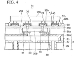
- connection portions B to which bumps of an upper semiconductor chip are connected later, in the third wiring patterns 32b are drawn.
- solder resist film 38 having an opening portion 38a for exposing the connection portions B of the third wiring patterns 32b in a lump is formed.
- the solder resist film 38 is formed so as to surround a packaging area where the upper semiconductor chip is mounted later.
- connection portions B of the third wiring patterns 32b fine ones at a pitch of approximately 150 ⁇ m (e.g., line: 100 ⁇ m, space: 50 ⁇ m) or less are illustrated. Accordingly, if a continuous solder resist film having opening portions for exposing respective main parts of the connection portions B of the third wiring patterns 32b is formed, there are cases where the opening portions of the solder resist film are formed in the state of being shifted from the main parts of the connection portions B due to displacement in the forming process. If the opening portions of the solder resist film are placed in the state of being shifted from the main parts of the connection portions B, the bonding areas between the bumps of the upper semiconductor chip and the connection portions B are reduced. Therefore, bonding failures and the like are apt to occur with decrease in the bonding strength of the bumps.
- patterns of the solder resist film 38 are not formed in the packaging area where the connection portions B of the third wiring patterns 32b are placed, but the opening portion 38a is provided in the packaging area in a lump.
- the connection portions B of the third wiring patterns 32b troubles that the bonding area for flip-chip bonding becomes small do not occur.
- Ni films 40 and Au films 42 are selectively sequentially formed on the third wiring patterns 32b exposed in the opening portion 38a by electroless plating. Note that the Ni films 40 may be omitted in the case where barrier films are not required.
- the upper semiconductor chip 20x (upper electronic parts) having bumps 21 is prepared, and the bumps 21 of the upper semiconductor chip 20x are flip-chip bonded to the Au films 42 of the connection portions B of the third wiring patterns 32b.
- the bumps 21 of the upper semiconductor chip 20x Au bumps or solder bumps are used. In the case where Au bumps are used, Au-Au bonding is performed using ultrasonic waves. Meanwhile, in the case where solder bumps are used, bonding is performed by reflow heating.
- the solder resist film 38 does not exist in the packaging area where the connection portions B of the third wiring patterns 32b are placed. Accordingly, the bumps 21 of the upper semiconductor chip 20x are bonded to the connection portions B of the third wiring patterns 32b with high reliability in the state where necessary bonding areas can be obtained.
- the second interlayer insulating film 36 is formed in a planarized state over all, the respective connection portions B of the third wiring patterns 32b are placed at almost the same height. Therefore, the occurrence of bonding failures between the upper semiconductor chip 20x and the connection portions B of the third wiring patterns 32b is prevented.
- bumps are formed on the connection portions B of the third wiring patterns 32b by mounting solder bolls thereon, and connection terminals of the upper semiconductor chip 20x are bonded to these bumps.
- connection portions B of the third wiring patterns 32b are at a fine pitch of approximately 150 ⁇ m or less, the bumps 21 of the upper semiconductor chip 20x can be flip-chip bonded to the connection portions B of the third wiring patterns 32b with high reliability.
- the size of the opening portion 38a of the solder resist film 38 is appropriately adjusted in accordance with the size of the upper semiconductor chip 20x so that the dimensions from the peripheral portion of the upper semiconductor chip 20x to the side surfaces of the opening portion 38a of the solder resist film 38 may be 0.5 to 2 mm (preferably, approximately 1 mm).
- the gap between an element formation surface (under surface) of the upper semiconductor chip 20x and the third wiring patterns 32b and the gap between the element formation surface of the upper semiconductor chip 20x and the second interlayer insulating film 36 are filled with underfill resin 35.
- the underfill resin 35 is filled in the gap under the under surface of the upper semiconductor chip 20x and formed in the state of being blocked by the side surfaces of the opening portion 38a of the solder resist film 38.
- the above-described mode in which the solder resist film 38 is not formed in the packaging area where the respective connection portions B of the third wiring patterns 32b are placed is one preferred example when the upper semiconductor chip 20x having the bumps 21 at a fine pitch is flip-chip bonded. Therefore, a mode in which a solder resist film 38 having opening portions for the main parts of the respective connection portions B of the third wiring patterns 32b is continuously formed in the packaging area may be adopted.
- the first insulating film 36a having the opening portion 39 in the packaging area A of the wiring substrate 2 is formed.
- the semiconductor chip 20 is flip-chip mounted on the connection portions B of the second wiring patterns 32a in the opening portion 39 of the first insulating film 36a.
- the gap under the under surface of the semiconductor chip 20 and the gap adjacent to the side surfaces thereof are filled with the underfill resin 36c in an integrated state.
- the backside (upper surface) of the semiconductor chip 20, the upper surface of the first insulating film 36a, and the upper surface of the underfill resin 36c are adjusted to almost the same height, and planarized by eliminating steps due to the thickness of the semiconductor chip 20. Further, the second insulating film for covering the semiconductor chip 20 is formed in the state where the upper surface of the second insulating film is planarized.
- the semiconductor chip 20 is flip-chip mounted on the connection portions B of the second wiring patterns 32a in the state where the semiconductor chip 20 is buried in the planar second interlayer insulating film 36 composed of the first insulating film 36a, the second insulating film 36b, and the underfill resin 36c.
- the second via holes 36x are formed in predetermined portions of the second interlayer insulating film 36 on the second wiring patterns 32a, and the third wiring patterns 32b connected to the second wiring patterns 32a through the second via holes 36x are formed on the second interlayer insulating film 36.
- the bumps 21 of the upper semiconductor chip 20x are flip-chip bonded to the connection portions B of the third wiring patterns 32b. Furthermore, the gap under the under surface of the upper semiconductor chip 20x is filled with the underfill resin 35.
- the semiconductor chip 20 is flip-chip mounted in the opening portion 39 of the first insulating film 36a partly constituting the second interlayer insulating film.
- the semiconductor device 1 of the present embodiment has a structure in which steps due to the thickness of the semiconductor chip 20 are eliminated with the first insulating film 36a.
- the second insulating film 36b for covering the semiconductor chip 20 is formed in the state where the upper surface of the second insulating film 36b is planar, the third wiring patterns 32b formed on the second insulating film 36b are stably formed with high precision. Moreover, since the connection portions B of the third wiring patterns 32b are placed at almost the same height, reliability of bonding between the bumps 21 of the upper semiconductor chip 20x and the connection portions B of the third wiring patterns 32b can be improved.
- a packaging structure in which a plurality of semiconductor chips 20 are three-dimensionally multilayered to be mutually connected in the state of being buried in respective interlayer insulating films is easily manufactured without the occurrence of any trouble.
- FIGS. 2A to 2F are sectional views showing a method of manufacturing an electronic parts packaging structure of a second embodiment of the present invention in order.
- the second embodiment is different from the first embodiment in that a semiconductor chip having a protection film provided on the backside thereof is used and in that an insulating film for covering the semiconductor chip is not formed.
- similar steps to those of the first embodiment will not be further described in detail.
- a wiring substrate 2 similar to that of FIG. 1C in the first embodiment is prepared.
- a semiconductor chip 20a electronic parts
- the semiconductor chip 20a is one thinned to a thickness of approximately 150 ⁇ m (preferably, approximately 50 ⁇ m) or less.
- protection film 44 epoxy series resin, polyimide series resin, polyphenylene ether series resin, acrylic series resin, or the like is used.
- a method of forming the protection film 44 a method of laminating a resin film, a method of forming a resin film by spin coating or the dip method, or the like is employed.
- the protection film 44 may be formed after silane coupling agent is coated on the backside of the semiconductor chip 20a.
- the bumps 21 of the semiconductor chip 20a are flip-chip bonded to Au films 37 of second wiring patterns 32a exposed in an opening portion 39 (packaging area A) of a first insulating film 36a by a similar method to that of the first embodiment.
- the gap under the under surface of the semiconductor chip 20a and the gap adjacent to the side surfaces thereof are filled with underfill resin 36c (filling resin film).
- underfill resin 36c filling resin film
- a second insulating film does not need to be formed on the semiconductor chip 20a, unlike the first embodiment. Accordingly, in the present embodiment, a second interlayer insulating film 36 in which the semiconductor chip 20a is buried is composed of the insulating film 36a, the protection film 44, and the underfill resin 36c.
- predetermined portions of the second interlayer insulating film 36 on the second wiring patterns 32a are etched by a laser or RIE, thereby forming second via holes 36x having depths reaching the second wiring patterns 32a.
- third wiring patterns 32b (upper wiring patterns) connected to the second wiring patterns 32a through the second via holes 36x are formed on the second interlayer insulating film 36 by a similar method to that of the first embodiment.
- solder resist film 38 having an opening portion 38a for exposing respective connection portions B of the third wiring patterns 32b in a lump is formed on the structure of the FIG. 2D. Furthermore, Ni films 40 and Au films 42 are sequentially formed on the connection portions B of the third wiring patterns 32b by electroless plating.
- bumps 21 of an upper semiconductor chip 20x are flip-chip bonded to the Au films 42 of the connection portions B of the third wiring patterns 32b by a similar method to that of the first embodiment. Thereafter, similar to the first embodiment, the gap under the upper semiconductor chip 20x is filled with underfill resin 35.
- the manufacturing method is simplified compared to a method in which a second insulating film for covering the semiconductor chip is formed as in the first embodiment, and the cost of manufacture can be reduced.
- a semiconductor device can be made thinner than the first embodiment by use of the semiconductor chip 20a having the protection film 44 on the backside thereof.
- FIGS. 3A to 3E are sectional views showing a method of manufacturing an electronic parts packaging structure of a third embodiment of the present invention in order.
- the third embodiment is different from the first and second embodiments in that, after a semiconductor chip is flip-chip mounted, via holes penetrating the semiconductor chip are formed therein, thus achieving mutual connection.
- similar steps to those of the first embodiment will not be further described in detail.
- a wiring substrate 2 having a similar structure to that of FIG. 1C in the first embodiment is prepared.
- a semiconductor chip 20b which has connection pads 23 and bumps 21 connected thereto on an element formation surface thereof and has a protection film 44 similar to that of the second embodiment on the backside thereof, is prepared.
- the connection pads 23 of the semiconductor chip 20b are obtained by rearranging electrode pads (not shown), which are arranged on the peripheral portion of the semiconductor chip 20b in a peripheral type arrangement, to an area array type arrangement by rewiring with Cu wirings.
- connection pads 23 and the bumps 21 connected thereto are examples of connection terminals.
- the gap under the under surface of the semiconductor chip 20b and the gap adjacent to the side surfaces thereof are filled with underfill resin 36c (filling insulating film) by a similar method to that of the first embodiment.
- underfill resin 36c filling insulating film
- a planarized second interlayer insulating film 36 composed of the insulating film 36a, the protection film 44 and the underfill resin 36c is obtained.
- second via holes 19 having depths reaching the connection pads 23 are formed by a laser or RIE in predetermined portions of the semiconductor chip 20b and the protection film 44 on the areas of the connection pads 23 except the areas to which the bumps 21 are bonded.
- the reason for forming the second via holes 19 on the connection pads in the areas except the areas to which the bumps 21 are bonded is that, if the second via holes 19 are formed above the areas to which the bumps 21 are bonded, damage can be caused at the joints between the connection pads 23 and the bumps 21 by a laser or RIE to lower reliability of bonding.
- third wiring patterns 32b (upper wiring patterns) connected to the connection pads 23 through the second via holes 19 formed in the semiconductor chip 20b are formed on the protection film 44 and the insulating film 36a through a semi-additive process, which has been described in the first embodiment, or the like.
- solder resist film 38 having an opening portion 38a for exposing connection portions B of the third wiring patterns 32b in a lump is formed.
- Ni films 40 and Au films 42 are sequentially formed on the respective connection portions B of the third wiring patterns 32b exposed in the opening portion 38a of the solder resist film 38 by a similar method to that of the first embodiment. Furthermore, after bumps 21 of an upper semiconductor chip 20x (upper electronic parts) having the bumps 21 are flip-chip bonded to the Au films 42 of the connection portions B of the third wiring patterns 32b, the gap under the under surface of the upper semiconductor chip 20x is filled with underfill resin 35.
- FIG. 4 is a sectional view showing the electronic parts packaging structure according to the modified example of the third embodiment of the present invention.
- a semiconductor chip 20b having no protection film 44 on the backside thereof is used. Moreover, after the semiconductor chip 20b is flip-chip bonded to second wiring patterns 32a and underfill resin 36c is filled, a second insulating film 36b is formed on the semiconductor chip 20b similarly to the first embodiment.
- the second insulating film 36b for covering the semiconductor chip 20b and the semiconductor chip 20b are etched by a laser or RIE in the step of forming second via holes 19. Furthermore, third wiring patterns 32b are formed on the second insulating film 36b. Other components are the same as those of FIG. 3E and therefore will not be further described.
- the third embodiment has similar effects to those of the first embodiment.
- wiring length can be shortened. Therefore, it can respond to speeding up of a signal speed in semiconductor devices for high-frequency applications.
- FIGS. 5A to 5G are sectional views showing a method of manufacturing an electronic parts packaging structure of a fourth embodiment of the present invention in order.
- the fourth embodiment is different from the first to third embodiments in that a semiconductor chip is mounted face up.
- similar steps to those of the first embodiment will not be further described in detail.
- a wiring substrate 2 similar to that of FIG. 1C in the first embodiment is prepared. Thereafter, a first insulating film 36a having an opening portion 39 in a packaging area A is formed on the wiring substrate 2 by a similar method to that of the first embodiment.
- a semiconductor chip is mounted face up in the packaging area A (opening portion 39). Therefore, unlike the first to third embodiments, an Au film does not need to be formed in a portion of a second wiring pattern 32a in the packaging area A.
- the packaging area A of the wiring substrate 2 exposed in the opening portion 39 of the first insulating film 36a may be any one of a portion of the second wiring pattern 32a as shown in FIG. 5A, a portion of a first interlayer insulating film 34, and a portion in which the second wiring pattern 32a and the first interlayer insulating film 34 exist together.
- connection pads 23 connection terminals
- the semiconductor chip 20c is fixed on the second wiring pattern 32a exposed in the opening portion 39 of the first insulating film 36a, with an adhesive layer 46 interposed therebetween in the state where the connection pads 23 of the semiconductor chip 20c are directed upward (face up).
- the element formation surface of the semiconductor chip 20c and the upper surface of the first insulating film 36a come to be at almost the same height, thus eliminating steps due to the thickness of the semiconductor chip 20c.
- a second insulating film 36b is formed on the semiconductor chip 20c and the first insulating film 36a.
- the second insulating film 36b is formed using material and a method similar to those of the first embodiment.
- the second insulating film 36b is formed in the state where the upper surface thereof is planarized without being affected by steps due to the thickness of the semiconductor chip 20c. At this time, the gap between the side surfaces of the semiconductor chip 20c and those of the opening portion 39 of the first insulating film 36a is filled with the second insulating film 36b to be planarized.
- a second interlayer insulating film 36 composed of the first and second insulating films 36a and 36b is obtained, and a structure in which the semiconductor chip 20c is buried in the planar second interlayer insulating film 36 and mounted face up, is formed.
- predetermined portions of the second interlayer insulating film 36 on the connection pads 23 of the semiconductor chip 20c are etched by a laser or RIE, thereby forming second via holes 36x having depths reaching the connection pads 23.
- a predetermined portion of the second interlayer insulating film 36 on the second wiring pattern 32a is simultaneously etched, thereby simultaneously forming a second via hole 36x having a depth reaching the second wiring pattern 32a.
- third wiring patterns 32b (upper wiring patterns), respectively connected to the connection pads 23 of the semiconductor chip 20c and the second wiring pattern 32a through the second via holes 36x, are formed on the second interlayer insulating film 36 through a semi-additive process, which is described in the first embodiment.
- the process from the step (FIG. 5B) of mounting the semiconductor chip 20c face up in the opening portion 39 of the first insulating film 36a to the step (FIG. 5E) of forming the third wiring patterns 32b may be repeated with a predetermined number of times.
- a packaging structure in which a plurality of semiconductor chips 20c are buried face up in respective interlayer insulating films and mutually connected through via holes can be easily obtained without the occurrence of any trouble.
- a solder resist film 38 having an opening portion 38a for exposing respective connection portions B of the third wiring patterns 32b in a lump is formed.
- Ni films 40 and Au films 42 are sequentially formed on the third wiring patterns 32b exposed in the opening portion 38a of the solder resist film 38.
- an upper semiconductor chip 20x (upper electronic parts) having bumps 21 is prepared, and the bumps 21 of the upper semiconductor chip 20x are flip-chip bonded to the Au films 42 of the connection portions B of the third wiring patterns 32b. Then, similar to the first embodiment, the gap under the under surface of the upper semiconductor chip 20x is filled with underfill resin 35.
- the first insulating film 36a having the opening portion 39 in the packaging area A is formed on the wiring substrate 2. Moreover, the semiconductor chip 20c is mounted in the opening portion 39 of the first insulating film 36a in the state where the connection pads 23 of the semiconductor chip 20c are directed upward (face up). Thus, steps due to the thickness of the semiconductor chip 20c are eliminated with the first insulating film 36a.
- the second insulating film 36b for covering the semiconductor chip 20c is formed in the state where the upper surface of the second insulating film 36b is planarized, and the second interlayer insulating film 36 is composed of the first and second insulating films 36a and 36b.
- the semiconductor chip 20c is mounted face up in the state of being buried in the planar second interlayer insulating film 36.
- a second via holes 36x are formed in the second interlayer insulating film 36 on the connection pads 23 of the semiconductor chip 20c and the second wiring pattern 32a respectively.
- the third wiring patterns 32b connected to the connection pads 23 and the second wiring pattern 32a through the second via holes 36x, are formed on the second interlayer insulating film 36.
- the bumps 21 of the upper semiconductor chip 20x are flip-chip bonded to the connection portions B of the third wiring patterns 32b.
- FIG. 6 is a sectional view showing the electronic parts packaging structure according to the modified example of the fourth embodiment of the present invention.
- a second insulating film 36b is not formed on a semiconductor chip 20c.
- an insulating film which has high reliability of dielectric resistance, and which has opening portions 25a on connection pads 23, is used as a passivation film 25 of the semiconductor chip 20c.
- the material and thickness thereof are not particularly limited.
- the passivation film 25 is composed of a silicon nitride film having a thickness of approximately 0.5 ⁇ m and a polyimide resin film having a thickness of approximately 3 ⁇ m or more.
- a resin film having opening portions for exposing the connection pads 23 may be attached to the semiconductor chip 20c to become the passivation film 25.
- the gap between the side surfaces of the semiconductor chip 20c and those of the opening portion 39 of the first insulating film 36a is filled with underfill resin 36c to completely achieve planarization.
- the first insulating film 36a on a second wiring pattern 32a is etched, thereby forming a second via holes 36x.
- third wiring patterns 32b which are connected to the second wiring pattern 32a through the second via holes 36x and which are connected to the connection pads 23 through the opening portions 25a of the passivation film 25 are formed on the first insulating film 36a and the passivation film 25.
- a second insulating film 36b for covering the semiconductor chip 20c can be omitted.
- Other components are the same as those of FIG. 5G and therefore will not be further described.
- the semiconductor chip 20c is mounted face up in the opening portion 39 of the first insulating film 36a. Accordingly, similar to the case where a semiconductor chip is flip-chip mounted face down as in the first to third embodiments, steps due to the thickness of the semiconductor chip 20c are easily eliminated with the first insulating film 36a. Therefore, the fourth embodiment has similar effects to those of the first embodiment.
Applications Claiming Priority (2)
| Application Number | Priority Date | Filing Date | Title |
|---|---|---|---|
| JP2003035156A JP4137659B2 (ja) | 2003-02-13 | 2003-02-13 | 電子部品実装構造及びその製造方法 |
| JP2003035156 | 2003-02-13 |
Publications (2)
| Publication Number | Publication Date |
|---|---|
| EP1447850A2 true EP1447850A2 (de) | 2004-08-18 |
| EP1447850A3 EP1447850A3 (de) | 2010-07-21 |
Family
ID=32677606
Family Applications (1)
| Application Number | Title | Priority Date | Filing Date |
|---|---|---|---|
| EP04250677A Withdrawn EP1447850A3 (de) | 2003-02-13 | 2004-02-09 | Elektronikteil-Gehäusungsstruktur und ihre Herstellungsmethode |
Country Status (6)
| Country | Link |
|---|---|
| US (4) | US7057290B2 (de) |
| EP (1) | EP1447850A3 (de) |
| JP (1) | JP4137659B2 (de) |
| KR (1) | KR101041011B1 (de) |
| CN (1) | CN1521847A (de) |
| TW (1) | TWI331389B (de) |
Cited By (3)
| Publication number | Priority date | Publication date | Assignee | Title |
|---|---|---|---|---|
| EP1761116A3 (de) * | 2005-08-26 | 2007-11-07 | Shinko Electric Industries Co., Ltd. | Mit elektronischen Komponenten versehene Leiterplatte durch Verwendung von Unterfüllungsmaterial und Herstellungsverfahren für solch eine Leiterplatte |
| EP1656005A3 (de) * | 2004-11-08 | 2007-11-14 | Shinko Electric Industries Co., Ltd. | Substrat mit einem Durchgangsloch und einer Verdrahtung verbunden mit diesem Durchgangsloch, und ein Herstellungsverfahren dafür |
| US8609539B2 (en) | 2005-11-02 | 2013-12-17 | Canon Kabushiki Kaisha | Embedded semiconductor device substrate and production method thereof |
Families Citing this family (65)
| Publication number | Priority date | Publication date | Assignee | Title |
|---|---|---|---|---|
| US7548430B1 (en) | 2002-05-01 | 2009-06-16 | Amkor Technology, Inc. | Buildup dielectric and metallization process and semiconductor package |
| US9691635B1 (en) | 2002-05-01 | 2017-06-27 | Amkor Technology, Inc. | Buildup dielectric layer having metallization pattern semiconductor package fabrication method |
| US20050056458A1 (en) * | 2003-07-02 | 2005-03-17 | Tsuyoshi Sugiura | Mounting pad, package, device, and method of fabricating the device |
| US20050270748A1 (en) * | 2003-12-16 | 2005-12-08 | Phoenix Precision Technology Corporation | Substrate structure integrated with passive components |
| US10811277B2 (en) | 2004-03-23 | 2020-10-20 | Amkor Technology, Inc. | Encapsulated semiconductor package |
| US11081370B2 (en) | 2004-03-23 | 2021-08-03 | Amkor Technology Singapore Holding Pte. Ltd. | Methods of manufacturing an encapsulated semiconductor device |
| JP2005317861A (ja) * | 2004-04-30 | 2005-11-10 | Toshiba Corp | 半導体装置およびその製造方法 |
| US20050258533A1 (en) * | 2004-05-21 | 2005-11-24 | Matsushita Electric Industrial Co., Ltd. | Semiconductor device mounting structure |
| US7179738B2 (en) * | 2004-06-17 | 2007-02-20 | Texas Instruments Incorporated | Semiconductor assembly having substrate with electroplated contact pads |
| US7411303B2 (en) * | 2004-11-09 | 2008-08-12 | Texas Instruments Incorporated | Semiconductor assembly having substrate with electroplated contact pads |
| KR100632257B1 (ko) * | 2004-11-09 | 2006-10-11 | 삼성전자주식회사 | 액정 디스플레이 구동용 탭 패키지의 배선 패턴 구조 |
| JP4800606B2 (ja) | 2004-11-19 | 2011-10-26 | Okiセミコンダクタ株式会社 | 素子内蔵基板の製造方法 |
| TWI253714B (en) * | 2004-12-21 | 2006-04-21 | Phoenix Prec Technology Corp | Method for fabricating a multi-layer circuit board with fine pitch |
| JP4507101B2 (ja) * | 2005-06-30 | 2010-07-21 | エルピーダメモリ株式会社 | 半導体記憶装置及びその製造方法 |
| US20080024998A1 (en) * | 2005-07-20 | 2008-01-31 | Shih-Ping Hsu | Substrate structure integrated with passive components |
| US20080023821A1 (en) * | 2005-07-20 | 2008-01-31 | Shih-Ping Hsu | Substrate structure integrated with passive components |
| TWI297941B (en) * | 2005-10-13 | 2008-06-11 | Phoenix Prec Technology Corp | Semiconductor device with electroless plating metal connecting layer and method for fabricating the same |
| JP2007123524A (ja) * | 2005-10-27 | 2007-05-17 | Shinko Electric Ind Co Ltd | 電子部品内蔵基板 |
| US20070126085A1 (en) * | 2005-12-02 | 2007-06-07 | Nec Electronics Corporation | Semiconductor device and method of manufacturing the same |
| JP4668782B2 (ja) * | 2005-12-16 | 2011-04-13 | 新光電気工業株式会社 | 実装基板の製造方法 |
| US7592202B2 (en) * | 2006-03-31 | 2009-09-22 | Intel Corporation | Embedding device in substrate cavity |
| JP2008010552A (ja) * | 2006-06-28 | 2008-01-17 | Nec Electronics Corp | パワーアンプモジュール |
| TWI304719B (en) * | 2006-10-25 | 2008-12-21 | Phoenix Prec Technology Corp | Circuit board structure having embedded compacitor and fabrication method thereof |
| JP5042591B2 (ja) | 2006-10-27 | 2012-10-03 | 新光電気工業株式会社 | 半導体パッケージおよび積層型半導体パッケージ |
| DE102007022959B4 (de) * | 2007-05-16 | 2012-04-19 | Infineon Technologies Ag | Verfahren zur Herstellung von Halbleitervorrichtungen |
| US7863088B2 (en) * | 2007-05-16 | 2011-01-04 | Infineon Technologies Ag | Semiconductor device including covering a semiconductor with a molding compound and forming a through hole in the molding compound |
| TWI348213B (en) * | 2007-08-15 | 2011-09-01 | Packaging substrate structure with capacitor embedded therein and method for fabricating the same | |
| KR100876899B1 (ko) * | 2007-10-10 | 2009-01-07 | 주식회사 하이닉스반도체 | 반도체 패키지 |
| JP5353153B2 (ja) * | 2007-11-09 | 2013-11-27 | パナソニック株式会社 | 実装構造体 |
| US8093704B2 (en) * | 2008-06-03 | 2012-01-10 | Intel Corporation | Package on package using a bump-less build up layer (BBUL) package |
| US7851928B2 (en) * | 2008-06-10 | 2010-12-14 | Texas Instruments Incorporated | Semiconductor device having substrate with differentially plated copper and selective solder |
| US20100032194A1 (en) * | 2008-08-08 | 2010-02-11 | Ibiden Co., Ltd. | Printed wiring board, manufacturing method for printed wiring board and electronic device |
| JPWO2010101163A1 (ja) * | 2009-03-04 | 2012-09-10 | 日本電気株式会社 | 機能素子内蔵基板及びそれを用いた電子デバイス |
| TWI396242B (zh) | 2009-08-11 | 2013-05-11 | Pixart Imaging Inc | 微電子裝置、微電子裝置的製造方法、微機電封裝結構及其封裝方法 |
| US8247253B2 (en) | 2009-08-11 | 2012-08-21 | Pixart Imaging Inc. | MEMS package structure and method for fabricating the same |
| CN102001613B (zh) * | 2009-09-02 | 2014-10-22 | 原相科技股份有限公司 | 微电子装置及制造方法、微机电封装结构及封装方法 |
| JP5428667B2 (ja) * | 2009-09-07 | 2014-02-26 | 日立化成株式会社 | 半導体チップ搭載用基板の製造方法 |
| JP2011061004A (ja) | 2009-09-10 | 2011-03-24 | Elpida Memory Inc | 半導体装置及びその製造方法 |
| US8446017B2 (en) * | 2009-09-18 | 2013-05-21 | Amkor Technology Korea, Inc. | Stackable wafer level package and fabricating method thereof |
| US8796561B1 (en) * | 2009-10-05 | 2014-08-05 | Amkor Technology, Inc. | Fan out build up substrate stackable package and method |
| US8937381B1 (en) | 2009-12-03 | 2015-01-20 | Amkor Technology, Inc. | Thin stackable package and method |
| JP5136632B2 (ja) * | 2010-01-08 | 2013-02-06 | 大日本印刷株式会社 | 電子部品 |
| US20110215450A1 (en) * | 2010-03-05 | 2011-09-08 | Chi Heejo | Integrated circuit packaging system with encapsulation and method of manufacture thereof |
| JP5681374B2 (ja) * | 2010-04-19 | 2015-03-04 | 日東電工株式会社 | ダイシングテープ一体型半導体裏面用フィルム |
| CN102275862B (zh) * | 2010-06-11 | 2014-10-01 | 原相科技股份有限公司 | 微机电封装结构及其制造方法 |
| JP5581830B2 (ja) * | 2010-06-11 | 2014-09-03 | 富士通株式会社 | 部品内蔵基板の製造方法及び部品内蔵基板 |
| US9337116B2 (en) * | 2010-10-28 | 2016-05-10 | Stats Chippac, Ltd. | Semiconductor device and method of forming stepped interposer for stacking and electrically connecting semiconductor die |
| US9391046B2 (en) * | 2011-05-20 | 2016-07-12 | STATS ChipPAC Pte. Ltd. | Semiconductor device and method of forming 3D semiconductor package with semiconductor die stacked over semiconductor wafer |
| JP6452270B2 (ja) * | 2012-04-19 | 2019-01-16 | キヤノン株式会社 | プリント回路板および電子機器 |
| WO2013172847A1 (en) * | 2012-05-17 | 2013-11-21 | Intel Corporation | Film insert molding for device manufacture |
| US8872349B2 (en) | 2012-09-11 | 2014-10-28 | Intel Corporation | Bridge interconnect with air gap in package assembly |
| CN104321866B (zh) * | 2012-09-14 | 2018-03-02 | 瑞萨电子株式会社 | 半导体器件的制造方法 |
| KR102042033B1 (ko) * | 2012-10-30 | 2019-11-08 | 엘지이노텍 주식회사 | 칩 실장형 인쇄회로기판 및 그 제조방법 |
| JP5682678B2 (ja) * | 2013-08-28 | 2015-03-11 | 日立化成株式会社 | 半導体チップ搭載用基板及びその製造方法 |
| TWI567886B (zh) * | 2014-05-28 | 2017-01-21 | 南茂科技股份有限公司 | 晶片封裝結構以及晶片封裝結構的製作方法 |
| CN105789161B (zh) * | 2014-12-22 | 2019-07-12 | 恒劲科技股份有限公司 | 封装结构及其制法 |
| US20160240457A1 (en) * | 2015-02-18 | 2016-08-18 | Altera Corporation | Integrated circuit packages with dual-sided stacking structure |
| KR102340053B1 (ko) * | 2015-06-18 | 2021-12-16 | 삼성전기주식회사 | 인쇄회로기판 및 인쇄회로기판의 제조 방법 |
| JP2017050315A (ja) * | 2015-08-31 | 2017-03-09 | イビデン株式会社 | プリント配線板及びプリント配線板の製造方法 |
| JP2017050313A (ja) * | 2015-08-31 | 2017-03-09 | イビデン株式会社 | プリント配線板及びプリント配線板の製造方法 |
| KR20170091436A (ko) * | 2016-02-01 | 2017-08-09 | 삼성전자주식회사 | 영상 표시 장치 및 그 동작방법 |
| JP2017156700A (ja) * | 2016-03-04 | 2017-09-07 | 株式会社ジャパンディスプレイ | 表示装置 |
| DE102018111389A1 (de) * | 2017-11-15 | 2019-05-16 | Taiwan Semiconductor Manufacturing Company, Ltd. | Halbleitervorrichtung und Herstellungsverfahren |
| CN110545635B (zh) * | 2018-05-29 | 2021-09-14 | 鹏鼎控股(深圳)股份有限公司 | 多层电路板的制作方法 |
| KR102163059B1 (ko) * | 2018-09-07 | 2020-10-08 | 삼성전기주식회사 | 연결구조체 내장기판 |
Citations (12)
| Publication number | Priority date | Publication date | Assignee | Title |
|---|---|---|---|---|
| JPH04315458A (ja) * | 1991-04-15 | 1992-11-06 | Sony Corp | 多層配線基板およびその製造方法 |
| EP0635885A1 (de) * | 1993-07-22 | 1995-01-25 | Hughes Aircraft Company | Integriertes Schaltungsbauelement hoher Dichte und Verfahren zu seiner Herstellung |
| US5561085A (en) * | 1994-12-19 | 1996-10-01 | Martin Marietta Corporation | Structure for protecting air bridges on semiconductor chips from damage |
| EP1041631A2 (de) * | 1999-03-30 | 2000-10-04 | NGK Spark Plug Company Limited | Gedruckte Schaltung mit eingebautem Kondensator, Substrat mit gedruckter Schaltung und Kondensator |
| US20010002727A1 (en) * | 1997-09-16 | 2001-06-07 | Tsukasa Shiraishi | Semiconductor device and module of the same |
| US20010004130A1 (en) * | 1999-12-16 | 2001-06-21 | Mitsutoshi Higashi | Semiconductor device and production method thereof |
| JP2002184796A (ja) * | 2000-12-14 | 2002-06-28 | Matsushita Electric Ind Co Ltd | 半導体装置及びその製造方法 |
| WO2002054451A2 (fr) * | 2000-12-28 | 2002-07-11 | Thales | Procede d'empilage de circuits integres |
| EP1225629A2 (de) * | 2001-01-19 | 2002-07-24 | Matsushita Electric Industrial Co., Ltd. | Modul mit Einbaukomponente und seine Herstellungsmethode |
| US20020117743A1 (en) * | 2000-12-27 | 2002-08-29 | Matsushita Electric Industrial Co., Ltd. | Component built-in module and method for producing the same |
| EP1259103A1 (de) * | 2000-02-25 | 2002-11-20 | Ibiden Co., Ltd. | Mehrschichtige leiterplatte und verfahren zu ihrer herstellung |
| US6518649B1 (en) * | 1999-12-20 | 2003-02-11 | Sharp Kabushiki Kaisha | Tape carrier type semiconductor device with gold/gold bonding of leads to bumps |
Family Cites Families (14)
| Publication number | Priority date | Publication date | Assignee | Title |
|---|---|---|---|---|
| US5367765A (en) * | 1990-08-31 | 1994-11-29 | Nec Corporation | Method of fabricating integrated circuit chip package |
| JPH07123184B2 (ja) * | 1991-12-17 | 1995-12-25 | 日本無線株式会社 | 高密度実装回路基板の製造方法 |
| US5353498A (en) * | 1993-02-08 | 1994-10-11 | General Electric Company | Method for fabricating an integrated circuit module |
| JPH08167630A (ja) * | 1994-12-15 | 1996-06-25 | Hitachi Ltd | チップ接続構造 |
| JP2790122B2 (ja) * | 1996-05-31 | 1998-08-27 | 日本電気株式会社 | 積層回路基板 |
| KR100253363B1 (ko) * | 1997-12-02 | 2000-04-15 | 김영환 | 반도체 패키지용 기판과 그 기판을 이용한 랜드 그리드 어레이반도체 패키지 및 그들의 제조 방법 |
| JP2000332369A (ja) | 1999-05-25 | 2000-11-30 | Mitsui Mining & Smelting Co Ltd | プリント回路板及びその製造方法 |
| JP2000323645A (ja) | 1999-05-11 | 2000-11-24 | Shinko Electric Ind Co Ltd | 半導体装置及びその製造方法 |
| KR100668939B1 (ko) | 2000-08-21 | 2007-01-12 | 앰코 테크놀로지 코리아 주식회사 | 보드 레벨 반도체 장치 및 그 제조 방법 |
| JP4447143B2 (ja) * | 2000-10-11 | 2010-04-07 | 新光電気工業株式会社 | 半導体装置及びその製造方法 |
| JP4243922B2 (ja) | 2001-06-26 | 2009-03-25 | イビデン株式会社 | 多層プリント配線板 |
| US20030197285A1 (en) * | 2002-04-23 | 2003-10-23 | Kulicke & Soffa Investments, Inc. | High density substrate for the packaging of integrated circuits |
| KR100585677B1 (ko) | 2004-07-02 | 2006-06-07 | 엘지전자 주식회사 | LnCP 라이브러리에서의 메시지 처리 방법 |
| US20090007996A1 (en) * | 2005-05-12 | 2009-01-08 | Battelle Memorial Institute | Method for Vibrating a Substrate During Material Formation |
-
2003
- 2003-02-13 JP JP2003035156A patent/JP4137659B2/ja not_active Expired - Fee Related
-
2004
- 2004-01-30 KR KR1020040005988A patent/KR101041011B1/ko active IP Right Grant
- 2004-02-05 US US10/771,506 patent/US7057290B2/en not_active Expired - Lifetime
- 2004-02-09 EP EP04250677A patent/EP1447850A3/de not_active Withdrawn
- 2004-02-09 TW TW093102945A patent/TWI331389B/zh not_active IP Right Cessation
- 2004-02-13 CN CNA2004100049508A patent/CN1521847A/zh active Pending
-
2006
- 2006-02-27 US US11/362,189 patent/US7545049B2/en not_active Expired - Lifetime
- 2006-09-22 US US11/524,933 patent/US7691673B2/en not_active Expired - Fee Related
-
2009
- 2009-04-21 US US12/385,814 patent/US7964950B2/en not_active Expired - Fee Related
Patent Citations (12)
| Publication number | Priority date | Publication date | Assignee | Title |
|---|---|---|---|---|
| JPH04315458A (ja) * | 1991-04-15 | 1992-11-06 | Sony Corp | 多層配線基板およびその製造方法 |
| EP0635885A1 (de) * | 1993-07-22 | 1995-01-25 | Hughes Aircraft Company | Integriertes Schaltungsbauelement hoher Dichte und Verfahren zu seiner Herstellung |
| US5561085A (en) * | 1994-12-19 | 1996-10-01 | Martin Marietta Corporation | Structure for protecting air bridges on semiconductor chips from damage |
| US20010002727A1 (en) * | 1997-09-16 | 2001-06-07 | Tsukasa Shiraishi | Semiconductor device and module of the same |
| EP1041631A2 (de) * | 1999-03-30 | 2000-10-04 | NGK Spark Plug Company Limited | Gedruckte Schaltung mit eingebautem Kondensator, Substrat mit gedruckter Schaltung und Kondensator |
| US20010004130A1 (en) * | 1999-12-16 | 2001-06-21 | Mitsutoshi Higashi | Semiconductor device and production method thereof |
| US6518649B1 (en) * | 1999-12-20 | 2003-02-11 | Sharp Kabushiki Kaisha | Tape carrier type semiconductor device with gold/gold bonding of leads to bumps |
| EP1259103A1 (de) * | 2000-02-25 | 2002-11-20 | Ibiden Co., Ltd. | Mehrschichtige leiterplatte und verfahren zu ihrer herstellung |
| JP2002184796A (ja) * | 2000-12-14 | 2002-06-28 | Matsushita Electric Ind Co Ltd | 半導体装置及びその製造方法 |
| US20020117743A1 (en) * | 2000-12-27 | 2002-08-29 | Matsushita Electric Industrial Co., Ltd. | Component built-in module and method for producing the same |
| WO2002054451A2 (fr) * | 2000-12-28 | 2002-07-11 | Thales | Procede d'empilage de circuits integres |
| EP1225629A2 (de) * | 2001-01-19 | 2002-07-24 | Matsushita Electric Industrial Co., Ltd. | Modul mit Einbaukomponente und seine Herstellungsmethode |
Cited By (5)
| Publication number | Priority date | Publication date | Assignee | Title |
|---|---|---|---|---|
| EP1656005A3 (de) * | 2004-11-08 | 2007-11-14 | Shinko Electric Industries Co., Ltd. | Substrat mit einem Durchgangsloch und einer Verdrahtung verbunden mit diesem Durchgangsloch, und ein Herstellungsverfahren dafür |
| US7365436B2 (en) | 2004-11-08 | 2008-04-29 | Shinko Electric Industries Co., Ltd. | Substrate having a penetrating via and wiring connected to the penetrating via and a method for manufacturing the same |
| EP1761116A3 (de) * | 2005-08-26 | 2007-11-07 | Shinko Electric Industries Co., Ltd. | Mit elektronischen Komponenten versehene Leiterplatte durch Verwendung von Unterfüllungsmaterial und Herstellungsverfahren für solch eine Leiterplatte |
| US7663253B2 (en) | 2005-08-26 | 2010-02-16 | Shinko Electric Industries Co., Ltd. | Board having electronic parts mounted by using under-fill material and method for producing the same |
| US8609539B2 (en) | 2005-11-02 | 2013-12-17 | Canon Kabushiki Kaisha | Embedded semiconductor device substrate and production method thereof |
Also Published As
| Publication number | Publication date |
|---|---|
| US20060145359A1 (en) | 2006-07-06 |
| US20090206471A1 (en) | 2009-08-20 |
| US20040178510A1 (en) | 2004-09-16 |
| JP2004247475A (ja) | 2004-09-02 |
| US20070013048A1 (en) | 2007-01-18 |
| JP4137659B2 (ja) | 2008-08-20 |
| US7545049B2 (en) | 2009-06-09 |
| US7691673B2 (en) | 2010-04-06 |
| TWI331389B (en) | 2010-10-01 |
| US7057290B2 (en) | 2006-06-06 |
| KR101041011B1 (ko) | 2011-06-16 |
| EP1447850A3 (de) | 2010-07-21 |
| KR20040073301A (ko) | 2004-08-19 |
| CN1521847A (zh) | 2004-08-18 |
| TW200416997A (en) | 2004-09-01 |
| US7964950B2 (en) | 2011-06-21 |
Similar Documents
| Publication | Publication Date | Title |
|---|---|---|
| US7057290B2 (en) | Electronic parts packaging structure and method of manufacturing the same | |
| US7573135B2 (en) | Electronic parts packaging structure in which a semiconductor chip is mounted on a wiring substrate and buried in an insulation film | |
| JP4251421B2 (ja) | 半導体装置の製造方法 | |
| JP3813402B2 (ja) | 半導体装置の製造方法 | |
| EP1427006B1 (de) | Verpackungsstruktur für elektronische Bauteile und Methode zu deren Herstellung | |
| KR101096614B1 (ko) | 전자 부품 실장 구조 및 그 제조 방법 | |
| US7122901B2 (en) | Semiconductor device | |
| US7723838B2 (en) | Package structure having semiconductor device embedded within wiring board | |
| US7791206B2 (en) | Semiconductor device and method of manufacturing the same | |
| JP4198566B2 (ja) | 電子部品内蔵基板の製造方法 | |
| JP2001024089A (ja) | システム半導体装置及びシステム半導体装置の製造方法 |
Legal Events
| Date | Code | Title | Description |
|---|---|---|---|
| PUAI | Public reference made under article 153(3) epc to a published international application that has entered the european phase |
Free format text: ORIGINAL CODE: 0009012 |
|
| AK | Designated contracting states |
Kind code of ref document: A2 Designated state(s): AT BE BG CH CY CZ DE DK EE ES FI FR GB GR HU IE IT LI LU MC NL PT RO SE SI SK TR |
|
| AX | Request for extension of the european patent |
Extension state: AL LT LV MK |
|
| PUAL | Search report despatched |
Free format text: ORIGINAL CODE: 0009013 |
|
| AK | Designated contracting states |
Kind code of ref document: A3 Designated state(s): AT BE BG CH CY CZ DE DK EE ES FI FR GB GR HU IE IT LI LU MC NL PT RO SE SI SK TR |
|
| AX | Request for extension of the european patent |
Extension state: AL LT LV MK |
|
| 17P | Request for examination filed |
Effective date: 20110117 |
|
| AKX | Designation fees paid |
Designated state(s): DE FR |
|
| 17Q | First examination report despatched |
Effective date: 20110628 |
|
| STAA | Information on the status of an ep patent application or granted ep patent |
Free format text: STATUS: THE APPLICATION IS DEEMED TO BE WITHDRAWN |
|
| 18D | Application deemed to be withdrawn |
Effective date: 20120110 |