EP1267401A2 - Halbleiter und seine Herstellung - Google Patents
Halbleiter und seine Herstellung Download PDFInfo
- Publication number
- EP1267401A2 EP1267401A2 EP02291418A EP02291418A EP1267401A2 EP 1267401 A2 EP1267401 A2 EP 1267401A2 EP 02291418 A EP02291418 A EP 02291418A EP 02291418 A EP02291418 A EP 02291418A EP 1267401 A2 EP1267401 A2 EP 1267401A2
- Authority
- EP
- European Patent Office
- Prior art keywords
- electrode pad
- semiconductor device
- hole
- forming
- semiconductor
- Prior art date
- Legal status (The legal status is an assumption and is not a legal conclusion. Google has not performed a legal analysis and makes no representation as to the accuracy of the status listed.)
- Withdrawn
Links
Images


Classifications
-
- H10W90/00—
-
- H10W20/0238—
-
- H10W20/20—
-
- H10W70/656—
-
- H10W72/019—
-
- H10W72/07251—
-
- H10W72/20—
-
- H10W72/244—
-
- H10W72/9226—
-
- H10W72/923—
-
- H10W72/9415—
-
- H10W72/942—
-
- H10W72/944—
-
- H10W90/297—
-
- H10W90/722—
Definitions
- the present invention relates to a semiconductor device and a method of production of the same, more particularly relates to a technique useful for reducing the size of a semiconductor device.
- a semiconductor device to be mounted on a motherboard has been comprised of a semiconductor chip mounted on a wiring board called an "interposer". This interposer has been considered necessary for aligning the positions of the electrode terminals of the semiconductor chip and motherboard.
- the thickness of the semiconductor device increases by the amount of that thickness, so it is preferable not to use such an interposer as much as possible so as to meet with the recent demands for reducing the size of electronic equipment.
- FIG. 12A A sectional view of such a semiconductor device of the related art is shown in FIG. 12A.
- the semiconductor device 101 of the related art is mainly comprised of a silicon substrate 102 and does not have an interposer.
- One surface 102a of the silicon substrate 102 has formed on it an electronic element formation layer 103 including a transistor or other electronic element. This is electrically connected with a via hole electrode pad 110.
- An insulating film 104 prevents electrical connection of the via hole electrode pad 110 or main electrode pad 105 with the silicon substrate 102.
- the semiconductor element formation layer 103 and via hole electrode pad 110 have stacked over them an SiO 2 film 106 and an interconnection pattern 107.
- the SiO 2 film 106 has a via hole 106a opened in it.
- the interconnection pattern 107 and via hole electrode pad 110 are electrically connected through this opening.
- the via hole electrode pad 110 is provided integrally with the main electrode pad 105. Further, the main electrode pad 105 and the silicon substrate 102 under it have a through hole 102c opened in them.
- the through hole 102c is a characterizing feature of this type of semiconductor device and is provided to lead out the interconnection pattern 107 to the other surface 102b of the silicon substrate 102.
- the interconnection pattern 107 led out to the other surface 102b is provided with solder bumps 108 functioning as external connection terminals to be aligned in position with the terminals of the motherboard (not shown).
- FIG. 12B is a plan view of the semiconductor device 101 seen from the direction of the arrow A of FIG. 12A.
- the interconnection pattern 107 is omitted.
- the via hole 106a is a wide diameter circle at the bottom of which the via hole electrode pad 110 is exposed.
- the semiconductor device 101 is fabricated by building in a structure new to the existing semiconductor device (LSI etc.) 109 shown in section in FIG. 12C.
- the main electrode pad 105 is provided at the existing semiconductor device 109 as well. This is the location where originally bonding wires, stud bumps, etc. are bonded, signals are input and output, and power is supplied.
- the via hole electrode pad 110 (FIG. 12B) is one of the new structures and is not provided in existing semiconductor devices 109.
- the via hole electrode pad 110 is newly provided to increase the contact area with the interconnection pattern 107 (FIG. 12A) by providing a wide-diameter via hole 106a above it and to prevent peeling with the interconnection pattern 107 due to stress and poor electrical contact arising due to the same.
- a via hole pad 110 is newly provided as a part for electrical connection with the interconnection pattern 107 and, to ensure reliable electrical connection, a wide-diameter circular via hole 106a is opened above the via hole electrode pad 110.
- via hole electrode pad 110 in addition to the existing main electrode pad 105 requires that the design of existing semiconductor devices be changed, so places a large burden on manufacturers of semiconductor devices (semiconductor manufacturers).
- An object of the present invention is to provide a semiconductor device, and a method of production of the same, enabling reliable electrical connection between an electrode pad and interconnection pattern without separate provision of a via hole use electrode pad in addition to the existing main electrode pad.
- a semiconductor device comprised of a semiconductor substrate; an electronic element formed on one surface of the semiconductor substrate; an electrode pad formed on that one surface and electrically connected with the element; a through hole passing through the electrode pad and the semiconductor substrate; an insulating film formed on at least the other surface of the semiconductor substrate, an inner wall of the through hole, and the electrode pad; a via hole provided in the insulating film on the electrode pad along an opening rim of the through hole; and an interconnection pattern electrically leading out the electrode pad to the other surface of the semiconductor substrate through the through hole and the via hole.
- the via hole is ring shaped.
- the via hole is arc shaped and a plurality of the via holes are provided.
- the via hole is dot shaped and a plurality of the via holes are provided.
- a diameter of the through hole is larger at a portion passing through the electrode pad than a portion passing through the semiconductor substrate.
- the electrode pad has a bottom electrode pad comprised of a first metal and a top electrode pad comprised of a second metal having a higher melting point than the first metal and formed on the bottom electrode pad. More preferably, the first metal is aluminum and the second metal is copper.
- the interconnection pattern electrically leads out the electrode pad to the one surface of the semiconductor substrate as well. It is possible to stack a plurality of these semiconductor devices together and electrically connect interconnection patterns of facing surfaces of each bottom semiconductor device and top semiconductor device through external connection terminals.
- the through holes are filled by a conductor electrically connected with the interconnection patterns. It is possible to stack a plurality of these semiconductor devices and electrically connect conductors filled in corresponding through holes of each bottom semiconductor device and top semiconductor device through external connection terminals.
- a method of production of a semiconductor device comprising the steps of forming an electronic element on one surface of a semiconductor substrate; forming an electrode pad electrically connected with the element on the one surface of the semiconductor substrate; forming a through hole passing through the electrode pad and the semiconductor substrate; forming an insulating film on at least the other surface of the semiconductor substrate, an inner wall of the through hole, and the electrode pad; forming a via hole exposing part of the electrode pad along an opening rim of the through hole by patterning the insulating film; forming a conductive film on the insulating film and in the via hole; and forming an interconnection pattern electrically leading the electrode pad to the other surface of the semiconductor substrate through the through hole and the via hole by patterning the conductive film.
- the step of forming a through hole includes the steps of forming a first opening in the electrode pad by patterning and forming a second opening in the semiconductor substrate including the element by firing through the first opening a laser beam of a smaller diameter than the diameter of the first opening, the through hole being defined by the first opening and the second opening.
- the step of forming the first opening and the step of forming the second opening include between them a step of polishing the other surface of the semiconductor substrate to reduce the thickness of the semiconductor substrate.
- the step of forming the via hole is performed by opening the insulating film by a laser beam.
- a ring-shaped via hole is formed by firing the laser beam on the insulating film in a ring shape.
- the step of forming an electrode pad includes the steps of forming a bottom electrode pad comprised of a first metal and forming a top electrode pad comprised of a second metal having a higher melting point than the first metal on the bottom electrode pad.
- a second metal having a higher melting point than the first metal on the bottom electrode pad.
- aluminum is used as the first metal and copper as the second metal.
- the interconnection pattern is formed so that the electrode pad is electrically led out to the one side of the semiconductor substrate as well. It is possible to provide the steps of preparing a plurality of such semiconductor devices and stacking the semiconductor devices in a plurality of layers by electrically connecting the interconnection patterns of the semiconductor device through external connection terminals.
- the method includes a step of filling the through holes by a conductor electrically connected to the conductive film after the step of forming the conductive film. It is possible to provide the steps of preparing a plurality of such semiconductor devices and stacking the semiconductor devices in a plurality of layers by electrically connecting the conductors exposed from openings of corresponding through holes of the plurality of semiconductor devices through external connection terminals.
- a semiconductor device is provided with a semiconductor substrate and an electronic element formed on one surface of the semiconductor substrate.
- An electrode pad electrically connected with this element is formed on that surface of the semiconductor substrate.
- the electrode pad and the semiconductor substrate have a through hole passing through them.
- An insulating film is formed on the inner wall of that through hole. This insulating film is further formed on the other surface of the semiconductor substrate and on the electrode pad.
- the portion formed on the electrode pad is provided with a via hole.
- An interconnection pattern electrically leading the electrode pad to the other surface of the semiconductor substrate through the via hole and the through hole is provided in the semiconductor device.
- the via hole in the insulating film around the opening rim of the through hole by providing the via hole in the insulating film around the opening rim of the through hole, the opening area of the via hole is secured and reliable electrical connection between the interconnection pattern and electrode pad is achieved. Due to this, in the present invention, the via hole electrode pad used in the past to secure the opening area of the via hole becomes unnecessary, so the planar size of the semiconductor device is made smaller than in the past.
- the diameter of the through hole is preferably made larger at the portion passing through the electrode pad (hereinafter called the "first opening”) than the portion passing through the semiconductor substrate (hereinafter called the "second opening").
- the interconnection pattern may electrically lead out the electrode pad to one surface of the semiconductor substrate.
- a method of production of a semiconductor device according to the present invention comprises the steps of:
- a via hole is formed along the opening rim of the through hole in the insulating film on the electrode pad by the step (e) among these steps. As explained above, due to the formation of this via hole, there is no need to use the via hole electrode pad in the present invention.
- step (c) (step of forming a through hole) may further include the steps of (c1) forming a first opening in the electrode pad by patterning and (c2) forming a second opening in the semiconductor substrate including the electronic element by firing through the first opening a laser beam of a smaller diameter than the diameter of the first opening.
- the through hole is defined by the first opening and the second opening.
- steps (c1) and (c2) since a laser beam of a smaller diameter than the diameter of the first opening is fired through the first opening after forming it, the laser beam can be prevented from contacting the first opening and vaporizing the material of the electrode pad, so the danger of the semiconductor substrate and the electrode pad ending up becoming electrically connected by vaporized material is lessened.
- this structure has the advantage that insulation between the electrode pad and semiconductor substrate at the side walls of the through hole is sufficiently secured.
- steps (c1) and (c2) may include between them a step of polishing the other surface of the semiconductor substrate to reduce the thickness of the semiconductor substrate.
- the semiconductor substrate is reduced in thickness before forming the second opening, it is possible to form the second opening by firing a laser beam for a short time and the heat damage to the semiconductor substrate arising due to the firing of the laser beam is reduced. Further, since the depth of working by the laser beam becomes shallow, the amount of vaporization of the material by the laser beam is reduced and the amount of the material vaporizing and depositing in the through hole is reduced. Due to this, it is possible to cleanly form the through hole.
- step (e) step of forming the via hole in the insulating film
- step (e) may be performed by opening the insulating film by a laser beam.
- step (b) step of forming the electrode pad
- step (b) step of forming the electrode pad
- the electrode pad becomes a two-layer structure of a bottom electrode pad and a top electrode pad. Further, the bottom electrode pad is protected by the top electrode pad having a higher melting point.
- the laser beam When forming a via hole in the insulating film by a laser beam, the laser beam has to pass through the insulating film, but by giving protection by the high melting point top electrode pad as explained above, the laser beam passing through the insulating film is prevented from passing through the electrode pad as well.
- FIGS. 1A, 1B, and 1C are sectional views of a semiconductor device according to a preferred embodiment of the present invention.
- FIG. 1B is an enlarged view of the area in the circle 1B of FIG. 1A
- FIG. 1C is an enlarged view of the area in the circle 1C of FIG. 1B
- the semiconductor device 215 is provided with a silicon substrate 201 (semiconductor substrate).
- a silicon substrate 201 semiconductor substrate
- One surface 201a of this silicon substrate 201 is formed with a semiconductor element formation layer 202 in which a transistor or other electronic element is built.
- the semiconductor element formation layer 202 has an electrode pad 211 provided on it. While not shown, the electrode pad 211 is electrically connected with an element in the semiconductor element formation layer 202.
- the electrode pad 211 and silicon substrate 201 have the element formation layer 202 interposed between them.
- Reference numeral 204 indicates a passivation layer provided to protect the semiconductor element formation layer 202.
- the layer is for example comprised of SiO 2 .
- Reference numeral 212 indicates a through hole passing through the electrode pad 211 and silicon substrate 201.
- An SiO 2 film 209 (insulating film) is formed on its inner walls. The SiO 2 film 209 is also formed on the other surface 201b of the silicon substrate 201 and on the electrode pad 211.
- the SiO 2 film 209 on the electrode pad 211 is provided with a via hole 209a of a characterizing feature of the present invention.
- the electrode pad 211 and an interconnection pattern 214 on the SiO 2 film are electrically connected through this via hole 209a.
- FIGS. 2A to 2D are plan views of the semiconductor device 215 shown in FIGS. 1A to 1C seen from the direction of the arrow A of FIG. 1A (from one surface 201a of the silicon substrate 201) and show various examples of the via holes 209a. Note that in these figures, the interconnection pattern 214 is omitted for facilitating the view of the via hole 209a.
- the via hole 209a electrically leads out the bottom electrode pad 211 by the interconnection pattern 214, so naturally is formed on the electrode pad 211.
- the electrode pad 211 is provided with an existing semiconductor device. That is, in the present invention, the interconnection pattern 214 is electrically connected to an existing electrode pad 211. A separate via hole electrode pad is not provided and connected there as in the related art.
- the via hole 209a is provided in a ring shape along the opening rim of the through hole 212, so a sufficient opening area is secured for reliably electrically connecting the interconnection pattern 214 and there is therefore no need to separately provide a via hole electrode pad as in the past.
- the planar size of the semiconductor device 215 can be made smaller than the past by that amount.
- the planar shape of the electrode pad 211 is substantially square with a length of each side of for example about 100 ⁇ m.
- the planar shape and size of the electrode pad 211 are not limited to these.
- the planar shape and size of the electrode pad 211 may be freely set.
- the width of the ring-shaped via hole 209a is for example about 5 to 10 ⁇ m, but the invention is not limited to this.
- FIG. 2B is an example of provision of the via hole 209a as an arc along the opening rim of the through hole 212.
- the arc-shaped via hole 209a need not be a single hole. It is also possible to provide a plurality as shown in FIG. 2C.
- FIG. 2D is an example of provision of a plurality of dot-shaped via holes 209a along the opening rim of the through hole 212.
- the shape of the via hole 209a is not limited to the above. What is important is that the via hole 209a be provided along the opening rim of the through hole 212. With a via hole 209a provided in this way, the above advantages of the present invention can be obtained.
- the through hole 212 is defined by the first opening 208 and the second opening 201c.
- the first opening 208 is the portion passing through the electrode pad 211
- the second opening 201c is the portion passing through the silicon substrate 201.
- the diameter R1 of the first opening 208 is made larger than the diameter R2 of the second opening 201c.
- R1 is about 50 to 70 ⁇ m, while R2 is made smaller than R1 or about 25 to 50 ⁇ m. What is important is that R1>R2.
- the present invention is not limited to the above numerical values.
- the diameters R1 and R2 are the same, it is possible to extend the distance D1 (FIG. 1C) between the near open ends 208a and 201d of the first opening 208 and second opening 201c. Therefore, it is possible to secure a sufficient insulation between the electrode pad 211 and silicon substrate 201 at the side walls of the through hole 212. Note that when the insulation is not particularly an issue, the diameters R1 and R2 may also be made the same.
- the second opening 201c is formed tapered, but as explained later, this is due to the formation of the second opening 201c by a laser beam.
- the shape is not limited to a tapered one.
- the advantages of the present invention can be obtained even if forming the second opening 201c straight in shape.
- the through hole 212 is hollow, but as shown in FIG. 10, it is also possible to fill the through hole 212 with a conductor 217 electrically connected with the interconnection pattern 214.
- the conductor 217 in this case, there is for example copper.
- this is formed over the SiO 2 film 209 and extends to the other surface 201b of the silicon substrate 201 through the through hole 212.
- the interconnection pattern 214 functions to electrically connect the electrode pad 211 to the other surface 201b through the via hole 209a and through hole 212.
- solder bumps 210 functioning as external connection terminals.
- the external connection terminals are not limited to the solder bumps 210. Stud bumps or other known external connection terminals may also be used.
- the semiconductor device 215 is electrically and mechanically connected on the motherboard.
- the semiconductor device 215 may be used alone in this way or may be used stacked as explained above.
- FIG. 3 is a plan view of the semiconductor device 215 seen from the A side of FIG. 1A.
- the interconnection pattern 214 formed on the surface 201a is provided with a terminal part 214a.
- This terminal part 214a is provided to electrically lead out the electrode pad 211 to the surface 201a of the silicon substrate 201.
- FIG. 4 A sectional view of semiconductor devices 215 stacked in this way is shown in FIG. 4. As shown in FIG. 4, the interconnection patterns of the facing surfaces of each top and bottom semiconductor device 215 are electrically connected through the solder bumps 210.
- This structure is a three-dimensional mounting structure obtained by stacking a plurality of the semiconductor devices. The planar size of each semiconductor device 215 is smaller than in the related art, so in this three-dimensional structure, it is possible to keep down the lateral spread as compared with the related art. This contributes to the higher density and smaller size of semiconductor packages as sought in recent years.
- the conductors 217a of the portions exposed from the openings 212a of the through holes 212 can be used instead of the terminal parts 214a, so the terminal parts 214a and the interconnection patterns 214 at the portions where solder bumps 210 are provided are unnecessary and the semiconductor devices 215 can be easily stacked.
- a sectional view of the semiconductor devices 215 in the case of stacking in this way is given in FIG. 11.
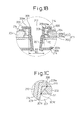
- FIGS. 5A to 5Q are sectional views of the semiconductor device in different steps of production.
- a silicon substrate 201 (semiconductor substrate) is prepared.
- This silicon substrate 201 is a substrate (wafer) for obtaining a large number of semiconductor devices.
- a transistor or other electronic element is formed on one surface 201a of the silicon substrate 201.
- reference numeral 202 shows a semiconductor element formation layer where the semiconductor element is formed.
- a film (not shown) comprised of aluminum (first metal) is formed on the electronic element formation layer 202 and this film patterned to form the bottom electrode pad 203.
- the thickness of the bottom electrode pad 203 is about 1 ⁇ m. Note that instead of aluminum, it is also possible to form the bottom electrode pad 203 by copper.
- the bottom electrode pad 203 and the silicon substrate 201 have the semiconductor element formation layer 202 interposed between them, the bottom electrode pad 203 is positioned above the silicon substrate 201 without contacting the silicon substrate 201. Further, while not particularly shown, the bottom electrode pad 203 is formed so as to be electrically connected with an interconnection layer in the semiconductor element formation layer 202.
- the bottom electrode pad 203 and the semiconductor element formation layer 202 have formed on them a passivation layer 204 comprised of SiO 2 etc.
- this passivation layer 204 is patterned to form an opening 204a where the bottom electrode pad 203 is exposed.
- the semiconductor substrate 201 formed with the bottom electrode pad 203 or semiconductor element formation layer 202 and the passivation layer 204 etc. is a general substrate usually produced by semiconductor manufacturers.
- the bottom electrode pad 203 is originally used as an electrode pad for wire bonding or bonding of external connection terminals (bumps etc.) (main electrode pad 110 in the example of the related art).
- a power feed layer 205a comprised of Cr (chrome) is formed on the passivation layer 204 and the exposed surface of the bottom electrode pad 203.
- the power feed layer 205a is formed by for example sputtering.
- a first photoresist 206 is coated on the power feed layer 205a.
- the first photoresist 206 is exposed and developed to form the first resist opening 206a superposed with the opening 204a of the passivation layer 204.
- the first photoresist 206 is removed, then the power feed layer 205a which had been formed under the first photoresist 206 is selectively etched to remove it.
- the top electrode pad 205 comprised of the power feed layer 205a and the electroplated copper layer 205b is completed.
- the thickness of the top electrode pad 205 is about 1 to 25 ⁇ m.
- the top electrode pad 205 is mainly comprised of copper (second metal) which has a higher melting point than the aluminum (first metal) comprising the bottom electrode pad 203.
- the bottom electrode pad 203 and the top electrode pad 205 form the electrode pad 211.
- a second photoresist 207 is formed on the passivation layer 204 and the exposed surface of the electrode pad 211. Further, the photoresist 207 is exposed and developed to form a second opening 207a exposing the electrode pad 211.
- the photoresist 207 is used as an etching mask to pattern the electrode pad 211 and form a first opening 208 in the electrode pad 211.
- the etching in this case is for example chemical etching or plasma etching.
- the diameter R1 of the first opening is about 50 to 70 ⁇ m, but should be suitably set in accordance with the diameter of the electrode pad 211.
- the other surface 201b of the silicon substrate 201 is polished to reduce the thickness of the silicon substrate 201 to about 50 to 150 ⁇ m.
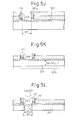
- a laser beam having a smaller diameter than the diameter R1 of the first opening 208 is fired through the first opening 208.
- the laser there is a UV laser, YAG laser, or excimer laser.
- the portion struck by the laser beam vaporizes, whereby a second opening 201c is formed in the silicon substrate 201.
- the diameter R2 of this second opening 201c is about 25 to 50 ⁇ m.
- the through hole 212 is defined by the first opening 208 and the second opening 201c.
- the laser beam By firing a laser beam of a diameter smaller than the diameter R1 after forming the first opening 208, the laser beam is prevented from contacting the first opening 208 and vaporizing the material of the electrode pad 211 (aluminum or copper), so the danger of vaporized material depositing on the side walls of the through hole 212 and electrically connecting the silicon substrate 201 and electrode pad 211 is reduced.
- the material of the electrode pad 211 aluminum or copper
- this structure has the advantage that the insulation between the electrode pad 211 and the silicon substrate 201 at the side walls of the through hole 212 can be sufficiently secured.
- the silicon substrate 201 is reduced in thickness at the step of FIG. 5K before forming the second opening 201c, it is possible to form the second opening 201c by firing the laser beam for a short time, so heat damage to the silicon substrate 201 arising due to the laser beam can be reduced.
- the depth of working by the laser beam becomes shallow, the amount of the silicon vaporized by the laser beam is reduced and the amount of the silicon which is vaporized and deposits in the through hole 212 is reduced. Due to this, it is possible to cleanly form the through hole 212.
- step of FIG. 5K step of reducing the thickness of the silicon substrate 201 may be omitted.
- the second opening 201c illustrated is tapered, this is because a laser beam focused to a point by a focusing lens (not shown) instead of a laser beam of parallel light is used.
- the second opening 201c does not have to be tapered in shape.
- the advantages of the present invention can be obtained even if the second opening 201c is formed straight in shape.
- the second opening 201c may be formed by firing the laser beam from the other surface 201b of the silicon substrate 201 instead of firing the laser beam through the first opening 208. Even when doing this, it is similarly possible to prevent silicon vaporized by the laser from depositing on the electrode pad 211.
- the step shown in FIG. 9 may be performed between the steps of FIG. 5K and FIG. 5L.
- an SiO 2 film or other protective film 216 is formed on the passivation layer 204, on the electrode pad 211, on the side walls of the first opening 208, and on the semiconductor element formation layer 202 exposed from the first opening 208.
- debris or burrs occur due to the laser beam, these are cleaned away (plasma cleaning or chemical washing).
- the protective film 216 is formed as explained above, it is possible to prevent damage to the electrode pad 211 or passivation layer 204 at the time of cleaning.
- an SiO 2 film 209 (insulating film) is formed at least on the other surface 201b of the semiconductor substrate 201, on the inner walls of the through hole 212, and on the electrode pad 211.
- the SiO 2 film 209 is formed by for example chemical vapor deposition (CVD).
- an SiO 2 film 209 may be formed on only the surface 201a of the semiconductor substrate 201 and the side walls of the through hole 212, then the SiO 2 film 209 formed on the other surface 201b.
- the SiO 2 film 209 is patterned to form the via hole 209a exposing part of the electrode pad 211 along the opening rim of the through hole 212.
- the shape of the via hole 209a is as shown in the already explained FIGS. 2A to 2D.
- the method of forming the via hole 209a shown in any of FIGS. 2A to 2D for example, it is possible to form a resist (not shown) having an opening corresponding to that shape on the SiO 2 film 209 and selectively etch the SiO 2 film through that opening.
- the etching technique used at that time is for example chemical etching or plasma etching.
- trepanning by the laser beam is suitable.
- This "trepanning" is the method of emitting a laser beam from a laser source and rotating that laser beam about its axis so as to make the laser beam draw a ring shape on the SiO 2 film 209.
- the method of firing the laser beam is not limited to trepanning.
- a light-shielding mask (not shown) having a window of a shape corresponding to the via hole 209a against the laser beam and open the via hole 209a by the laser beam passing through that window.
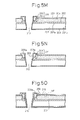
- the electrode pad 211 is made a two-layer structure of a bottom electrode pad 203 and a top electrode pad 205, the following advantages are obtained regardless of the method of firing the laser beam.
- the via hole 209a is a portion where the interconnection pattern 213 is electrically connected with the electrode pad 211, so to ensure reliable connection, it must pass all the way through. Therefore, when forming the via hole 209a so as to pass all the way through, the laser beam is fired by a power and time at least for passing through the SiO 2 film 209. At that time, as shown in FIGS. 7A and 7B, part 205c of the top electrode pad 205 also ends up being vaporized by the laser beam. The bottom electrode pad 203, however, is protected by the top electrode pad 205, so the laser beam will not pass through the bottom electrode pad 203 and reach the silicon substrate 201. In particular, a top electrode pad 205 made mainly of copper has a higher melting point than even the bottom electrode pad 203 made mainly of aluminum, so the bottom electrode pad 203 can be effectively protected.
- the bottom electrode pad 203 is formed by copper, it is possible to protect the bottom electrode pad 203 from the laser beam by an increased thickness of the top electrode pad 205. That is, even when the bottom electrode pad 203 and the top electrode pad 205 are the same material, by thickly forming the top electrode pad 205 and making the electrode pad 211 this two-layer structure, the bottom electrode pad 203 can be protected from the laser beam.
- the step of forming the top electrode pad 205 (step of FIGS. 5E to 5H) is unnecessary.
- the step of forming the top electrode pad 203 is unnecessary.
- the step shown in FIG. 50 is performed.
- the conductive film 213 is formed on the SiO 2 film 209 and in the via hole 209a.
- the thickness of the conductive film 213 is about 1 to 20 ⁇ m.
- the conductive film 213, as shown in FIG. 5P, is comprised of a Cr (chrome) film 213a formed by sputtering, a copper film 213b formed over it also by sputtering, and an electroplated copper film 213c formed using the Cr (chrome) film 213a and copper film 213b as power feed layers.
- the structure of the conductive film 213, however, is not limited to this.
- Cr (chrome) film by sputtering, then form a Cu (copper), Ni (nickel), Au (gold), or other film by elecroless plating or electroplating on the Cr (chrome) film for use as the conductive film 213.
- the through hole 212 is hollow, but the present invention is not limited to this.
- the method of filling is not limited to the above method.
- the conductive film 213 does not become thick, so it is possible to finely pattern the conductive layer 213 in a later step. Note that whatever the method, the conductor 217 should electrically connect with the conductive film 213.
- the conductive film 213 is patterned to form interconnection patterns 214.
- the interconnection patterns 214 are formed on the two main surfaces 201a and 201b of the silicon substrate 201.
- the interconnection patterns 214 of the two main surfaces 201a and 201b are electrically connected through the through hole 212.
- solder bumps 210 serving as external connection terminals, then the substrate is diced, whereby semiconductor devices as shown in FIG. 1A are completed.
- the completed semiconductor devices 215 may be mounted alone on a motherboard (not shown) or may be stacked.
- terminal parts 214a are provided at the interconnection patterns 214.
- a plurality of the completed semiconductor devices 215 are prepared.
- the solder bumps 210 are made to reflow in the state with the solder bumps 210 abutting against the terminal parts 214a of the bottom semiconductor devices 215. After reflow, the temperature of the solder bumps 215 falls, whereby a semiconductor module of a three-dimensional mounting structure comprised of a large number of stacked semiconductor devices 215 is completed.
- the conductors 217a of the portions exposed from the openings 212a of the through holes 212 function as the above terminal parts 214a, so the terminal parts 214a and the interconnection patterns 214 of the locations of provision of the solder bumps 210 are unnecessary.
- a via hole is provided in the insulating film along the opening rim of the through hole to secure a sufficient opening area of the via hole and reliably electrically connect the interconnection pattern and electrode pad. Due to this, in the present invention, the via hole electrode pad used in the past to secure the opening area of the via hole becomes unnecessary, so the planar size of the semiconductor chip can be made smaller than in the past.
- the diameter of the through hole can be made larger at the portion passing through the electrode pad than the portion passing through the semiconductor substrate. If this is done, insulation between the electrode pad and the semiconductor substrate can be sufficiently secured at the side walls of the through hole.
Landscapes
- Internal Circuitry In Semiconductor Integrated Circuit Devices (AREA)
Applications Claiming Priority (2)
| Application Number | Priority Date | Filing Date | Title |
|---|---|---|---|
| JP2001180891 | 2001-06-14 | ||
| JP2001180891A JP2002373957A (ja) | 2001-06-14 | 2001-06-14 | 半導体装置及びその製造方法 |
Publications (2)
| Publication Number | Publication Date |
|---|---|
| EP1267401A2 true EP1267401A2 (de) | 2002-12-18 |
| EP1267401A3 EP1267401A3 (de) | 2005-09-28 |
Family
ID=19021240
Family Applications (1)
| Application Number | Title | Priority Date | Filing Date |
|---|---|---|---|
| EP02291418A Withdrawn EP1267401A3 (de) | 2001-06-14 | 2002-06-07 | Halbleiter und seine Herstellung |
Country Status (5)
| Country | Link |
|---|---|
| US (1) | US6699787B2 (de) |
| EP (1) | EP1267401A3 (de) |
| JP (1) | JP2002373957A (de) |
| CN (1) | CN100364091C (de) |
| TW (1) | TW548826B (de) |
Cited By (2)
| Publication number | Priority date | Publication date | Assignee | Title |
|---|---|---|---|---|
| EP1577948A1 (de) * | 2004-03-16 | 2005-09-21 | Irvine Sensors Corp. | Mikroelektrisches Stapelmodul mit vertikalen Kontaktlöchern |
| EP1630867A3 (de) * | 2004-08-31 | 2010-06-02 | Seiko Epson Corporation | Verfahren zur Herstellung einer Halbleiter-Vorrichtung und Halbleiter-Vorrichtung |
Families Citing this family (88)
| Publication number | Priority date | Publication date | Assignee | Title |
|---|---|---|---|---|
| US20030057544A1 (en) * | 2001-09-13 | 2003-03-27 | Nathan Richard J. | Integrated assembly protocol |
| US20030059976A1 (en) * | 2001-09-24 | 2003-03-27 | Nathan Richard J. | Integrated package and methods for making same |
| US20030153119A1 (en) * | 2002-02-14 | 2003-08-14 | Nathan Richard J. | Integrated circuit package and method for fabrication |
| JP3972813B2 (ja) * | 2002-12-24 | 2007-09-05 | セイコーエプソン株式会社 | 半導体装置の製造方法 |
| JP3696208B2 (ja) * | 2003-01-22 | 2005-09-14 | 株式会社東芝 | 半導体装置 |
| JP2004297019A (ja) * | 2003-03-28 | 2004-10-21 | Seiko Epson Corp | 半導体装置、回路基板及び電子機器 |
| JP2004327910A (ja) * | 2003-04-28 | 2004-11-18 | Sharp Corp | 半導体装置およびその製造方法 |
| JP2004342990A (ja) * | 2003-05-19 | 2004-12-02 | Seiko Epson Corp | 半導体装置及びその製造方法、回路基板並びに電子機器 |
| JP2004349593A (ja) | 2003-05-26 | 2004-12-09 | Sanyo Electric Co Ltd | 半導体装置及びその製造方法 |
| TWI336220B (en) * | 2003-06-20 | 2011-01-11 | Japan Circuit Ind Co Ltd | A method of forming a high density printed wiring board for mounting a semiconductor |
| US8084866B2 (en) | 2003-12-10 | 2011-12-27 | Micron Technology, Inc. | Microelectronic devices and methods for filling vias in microelectronic devices |
| US7091124B2 (en) * | 2003-11-13 | 2006-08-15 | Micron Technology, Inc. | Methods for forming vias in microelectronic devices, and methods for packaging microelectronic devices |
| JP4307284B2 (ja) * | 2004-02-17 | 2009-08-05 | 三洋電機株式会社 | 半導体装置の製造方法 |
| US6943106B1 (en) * | 2004-02-20 | 2005-09-13 | Micron Technology, Inc. | Methods of fabricating interconnects for semiconductor components including plating solder-wetting material and solder filling |
| US20070176294A1 (en) * | 2004-03-26 | 2007-08-02 | Fujikura Ltd. | Thorough wiring board and method of manufacturing the same |
| US20050247894A1 (en) | 2004-05-05 | 2005-11-10 | Watkins Charles M | Systems and methods for forming apertures in microfeature workpieces |
| US7232754B2 (en) | 2004-06-29 | 2007-06-19 | Micron Technology, Inc. | Microelectronic devices and methods for forming interconnects in microelectronic devices |
| DE102004031878B3 (de) * | 2004-07-01 | 2005-10-06 | Epcos Ag | Elektrisches Mehrschichtbauelement mit zuverlässigem Lötkontakt |
| US7425499B2 (en) * | 2004-08-24 | 2008-09-16 | Micron Technology, Inc. | Methods for forming interconnects in vias and microelectronic workpieces including such interconnects |
| SG120200A1 (en) | 2004-08-27 | 2006-03-28 | Micron Technology Inc | Slanted vias for electrical circuits on circuit boards and other substrates |
| US7300857B2 (en) | 2004-09-02 | 2007-11-27 | Micron Technology, Inc. | Through-wafer interconnects for photoimager and memory wafers |
| JP4795677B2 (ja) * | 2004-12-02 | 2011-10-19 | ルネサスエレクトロニクス株式会社 | 半導体装置およびそれを用いた半導体モジュール、ならびに半導体装置の製造方法 |
| US7271482B2 (en) | 2004-12-30 | 2007-09-18 | Micron Technology, Inc. | Methods for forming interconnects in microelectronic workpieces and microelectronic workpieces formed using such methods |
| JP4577687B2 (ja) * | 2005-03-17 | 2010-11-10 | エルピーダメモリ株式会社 | 半導体装置 |
| US7317256B2 (en) * | 2005-06-01 | 2008-01-08 | Intel Corporation | Electronic packaging including die with through silicon via |
| US7795134B2 (en) * | 2005-06-28 | 2010-09-14 | Micron Technology, Inc. | Conductive interconnect structures and formation methods using supercritical fluids |
| JP4758712B2 (ja) | 2005-08-29 | 2011-08-31 | 新光電気工業株式会社 | 半導体装置の製造方法 |
| JP4533283B2 (ja) * | 2005-08-29 | 2010-09-01 | 新光電気工業株式会社 | 半導体装置の製造方法 |
| US7863187B2 (en) | 2005-09-01 | 2011-01-04 | Micron Technology, Inc. | Microfeature workpieces and methods for forming interconnects in microfeature workpieces |
| US7622377B2 (en) | 2005-09-01 | 2009-11-24 | Micron Technology, Inc. | Microfeature workpiece substrates having through-substrate vias, and associated methods of formation |
| US7262134B2 (en) | 2005-09-01 | 2007-08-28 | Micron Technology, Inc. | Microfeature workpieces and methods for forming interconnects in microfeature workpieces |
| JP5222459B2 (ja) * | 2005-10-18 | 2013-06-26 | 新光電気工業株式会社 | 半導体チップの製造方法、マルチチップパッケージ |
| US7892972B2 (en) * | 2006-02-03 | 2011-02-22 | Micron Technology, Inc. | Methods for fabricating and filling conductive vias and conductive vias so formed |
| KR100753415B1 (ko) * | 2006-03-17 | 2007-08-30 | 주식회사 하이닉스반도체 | 스택 패키지 |
| US7749899B2 (en) | 2006-06-01 | 2010-07-06 | Micron Technology, Inc. | Microelectronic workpieces and methods and systems for forming interconnects in microelectronic workpieces |
| US7629249B2 (en) | 2006-08-28 | 2009-12-08 | Micron Technology, Inc. | Microfeature workpieces having conductive interconnect structures formed by chemically reactive processes, and associated systems and methods |
| US7902643B2 (en) | 2006-08-31 | 2011-03-08 | Micron Technology, Inc. | Microfeature workpieces having interconnects and conductive backplanes, and associated systems and methods |
| JP4312786B2 (ja) * | 2006-11-02 | 2009-08-12 | Okiセミコンダクタ株式会社 | 半導体チップの製造方法 |
| US8569876B2 (en) | 2006-11-22 | 2013-10-29 | Tessera, Inc. | Packaged semiconductor chips with array |
| US7791199B2 (en) | 2006-11-22 | 2010-09-07 | Tessera, Inc. | Packaged semiconductor chips |
| JP5584474B2 (ja) | 2007-03-05 | 2014-09-03 | インヴェンサス・コーポレイション | 貫通ビアによって前面接点に接続された後面接点を有するチップ |
| WO2009017835A2 (en) * | 2007-07-31 | 2009-02-05 | Tessera, Inc. | Semiconductor packaging process using through silicon vias |
| SG150410A1 (en) | 2007-08-31 | 2009-03-30 | Micron Technology Inc | Partitioned through-layer via and associated systems and methods |
| US7884015B2 (en) | 2007-12-06 | 2011-02-08 | Micron Technology, Inc. | Methods for forming interconnects in microelectronic workpieces and microelectronic workpieces formed using such methods |
| KR101052870B1 (ko) * | 2008-04-21 | 2011-07-29 | 주식회사 하이닉스반도체 | 관통 전극, 이를 갖는 회로 기판, 이를 갖는 반도체 패키지및 반도체 패키지를 갖는 적층 반도체 패키지 |
| TWI389291B (zh) * | 2008-05-13 | 2013-03-11 | 財團法人工業技術研究院 | 三維堆疊晶粒封裝結構 |
| US8030780B2 (en) | 2008-10-16 | 2011-10-04 | Micron Technology, Inc. | Semiconductor substrates with unitary vias and via terminals, and associated systems and methods |
| TW201114003A (en) * | 2008-12-11 | 2011-04-16 | Xintec Inc | Chip package structure and method for fabricating the same |
| JP5471268B2 (ja) | 2008-12-26 | 2014-04-16 | 大日本印刷株式会社 | 貫通電極基板及びその製造方法 |
| CN101494951A (zh) * | 2009-02-18 | 2009-07-29 | 旭丽电子(广州)有限公司 | 印刷电路板 |
| JP2011009645A (ja) * | 2009-06-29 | 2011-01-13 | Toshiba Corp | 半導体装置及びその製造方法 |
| JP5574639B2 (ja) * | 2009-08-21 | 2014-08-20 | 三菱電機株式会社 | 半導体装置およびその製造方法 |
| TWI392069B (zh) * | 2009-11-24 | 2013-04-01 | 日月光半導體製造股份有限公司 | 封裝結構及其封裝製程 |
| WO2011118572A1 (ja) * | 2010-03-23 | 2011-09-29 | 日本電気株式会社 | 半導体装置の製造方法 |
| US8796135B2 (en) | 2010-07-23 | 2014-08-05 | Tessera, Inc. | Microelectronic elements with rear contacts connected with via first or via middle structures |
| US9640437B2 (en) | 2010-07-23 | 2017-05-02 | Tessera, Inc. | Methods of forming semiconductor elements using micro-abrasive particle stream |
| US8791575B2 (en) | 2010-07-23 | 2014-07-29 | Tessera, Inc. | Microelectronic elements having metallic pads overlying vias |
| TWI446420B (zh) | 2010-08-27 | 2014-07-21 | 日月光半導體製造股份有限公司 | 用於半導體製程之載體分離方法 |
| TWI445152B (zh) | 2010-08-30 | 2014-07-11 | 日月光半導體製造股份有限公司 | 半導體結構及其製作方法 |
| US9007273B2 (en) | 2010-09-09 | 2015-04-14 | Advances Semiconductor Engineering, Inc. | Semiconductor package integrated with conformal shield and antenna |
| US8847380B2 (en) | 2010-09-17 | 2014-09-30 | Tessera, Inc. | Staged via formation from both sides of chip |
| US8610259B2 (en) | 2010-09-17 | 2013-12-17 | Tessera, Inc. | Multi-function and shielded 3D interconnects |
| TWI434387B (zh) | 2010-10-11 | 2014-04-11 | 日月光半導體製造股份有限公司 | 具有穿導孔之半導體裝置及具有穿導孔之半導體裝置之封裝結構及其製造方法 |
| TWI527174B (zh) | 2010-11-19 | 2016-03-21 | 日月光半導體製造股份有限公司 | 具有半導體元件之封裝結構 |
| US8736066B2 (en) | 2010-12-02 | 2014-05-27 | Tessera, Inc. | Stacked microelectronic assemby with TSVS formed in stages and carrier above chip |
| US8637968B2 (en) | 2010-12-02 | 2014-01-28 | Tessera, Inc. | Stacked microelectronic assembly having interposer connecting active chips |
| US8587126B2 (en) | 2010-12-02 | 2013-11-19 | Tessera, Inc. | Stacked microelectronic assembly with TSVs formed in stages with plural active chips |
| US8610264B2 (en) | 2010-12-08 | 2013-12-17 | Tessera, Inc. | Compliant interconnects in wafers |
| TWI445155B (zh) | 2011-01-06 | 2014-07-11 | 日月光半導體製造股份有限公司 | 堆疊式封裝結構及其製造方法 |
| US8853819B2 (en) | 2011-01-07 | 2014-10-07 | Advanced Semiconductor Engineering, Inc. | Semiconductor structure with passive element network and manufacturing method thereof |
| JP5834563B2 (ja) * | 2011-07-14 | 2015-12-24 | セイコーエプソン株式会社 | 半導体装置の製造方法 |
| US8541883B2 (en) | 2011-11-29 | 2013-09-24 | Advanced Semiconductor Engineering, Inc. | Semiconductor device having shielded conductive vias |
| US8975157B2 (en) | 2012-02-08 | 2015-03-10 | Advanced Semiconductor Engineering, Inc. | Carrier bonding and detaching processes for a semiconductor wafer |
| US8963316B2 (en) | 2012-02-15 | 2015-02-24 | Advanced Semiconductor Engineering, Inc. | Semiconductor device and method for manufacturing the same |
| US8786060B2 (en) | 2012-05-04 | 2014-07-22 | Advanced Semiconductor Engineering, Inc. | Semiconductor package integrated with conformal shield and antenna |
| US9153542B2 (en) | 2012-08-01 | 2015-10-06 | Advanced Semiconductor Engineering, Inc. | Semiconductor package having an antenna and manufacturing method thereof |
| US8937387B2 (en) | 2012-11-07 | 2015-01-20 | Advanced Semiconductor Engineering, Inc. | Semiconductor device with conductive vias |
| US8952542B2 (en) | 2012-11-14 | 2015-02-10 | Advanced Semiconductor Engineering, Inc. | Method for dicing a semiconductor wafer having through silicon vias and resultant structures |
| US9406552B2 (en) | 2012-12-20 | 2016-08-02 | Advanced Semiconductor Engineering, Inc. | Semiconductor device having conductive via and manufacturing process |
| US8841751B2 (en) | 2013-01-23 | 2014-09-23 | Advanced Semiconductor Engineering, Inc. | Through silicon vias for semiconductor devices and manufacturing method thereof |
| US9978688B2 (en) | 2013-02-28 | 2018-05-22 | Advanced Semiconductor Engineering, Inc. | Semiconductor package having a waveguide antenna and manufacturing method thereof |
| US9089268B2 (en) | 2013-03-13 | 2015-07-28 | Advanced Semiconductor Engineering, Inc. | Neural sensing device and method for making the same |
| US8987734B2 (en) | 2013-03-15 | 2015-03-24 | Advanced Semiconductor Engineering, Inc. | Semiconductor wafer, semiconductor process and semiconductor package |
| US9173583B2 (en) | 2013-03-15 | 2015-11-03 | Advanced Semiconductor Engineering, Inc. | Neural sensing device and method for making the same |
| US10304765B2 (en) * | 2017-06-08 | 2019-05-28 | Advanced Semiconductor Engineering, Inc. | Semiconductor device package |
| KR102615701B1 (ko) * | 2018-06-14 | 2023-12-21 | 삼성전자주식회사 | 관통 비아를 포함하는 반도체 장치, 반도체 패키지 및 이의 제조 방법 |
| KR102695369B1 (ko) * | 2019-09-04 | 2024-08-16 | 삼성전자주식회사 | 반도체 소자 |
| JP2022029308A (ja) * | 2020-08-04 | 2022-02-17 | 新光電気工業株式会社 | 配線基板及び配線基板の製造方法 |
Family Cites Families (9)
| Publication number | Priority date | Publication date | Assignee | Title |
|---|---|---|---|---|
| US5065228A (en) * | 1989-04-04 | 1991-11-12 | Olin Corporation | G-TAB having particular through hole |
| US5527741A (en) * | 1994-10-11 | 1996-06-18 | Martin Marietta Corporation | Fabrication and structures of circuit modules with flexible interconnect layers |
| WO1996013062A1 (en) * | 1994-10-19 | 1996-05-02 | Ceram Incorporated | Apparatus and method of manufacturing stacked wafer array |
| US5874770A (en) * | 1996-10-10 | 1999-02-23 | General Electric Company | Flexible interconnect film including resistor and capacitor layers |
| JP2000246475A (ja) * | 1999-02-25 | 2000-09-12 | Seiko Epson Corp | レーザ光による加工方法 |
| JP4547728B2 (ja) * | 1999-03-29 | 2010-09-22 | ソニー株式会社 | 半導体装置及びその製造方法 |
| JP4438133B2 (ja) * | 1999-08-19 | 2010-03-24 | シャープ株式会社 | ヘテロ接合型バイポーラトランジスタおよびその製造方法 |
| JP4245754B2 (ja) * | 1999-11-02 | 2009-04-02 | パナソニック株式会社 | 半導体装置 |
| JP4053257B2 (ja) * | 2001-06-14 | 2008-02-27 | 新光電気工業株式会社 | 半導体装置の製造方法 |
-
2001
- 2001-06-14 JP JP2001180891A patent/JP2002373957A/ja active Pending
-
2002
- 2002-06-06 US US10/162,587 patent/US6699787B2/en not_active Expired - Fee Related
- 2002-06-07 EP EP02291418A patent/EP1267401A3/de not_active Withdrawn
- 2002-06-13 TW TW091112925A patent/TW548826B/zh not_active IP Right Cessation
- 2002-06-14 CN CNB021213437A patent/CN100364091C/zh not_active Expired - Fee Related
Cited By (2)
| Publication number | Priority date | Publication date | Assignee | Title |
|---|---|---|---|---|
| EP1577948A1 (de) * | 2004-03-16 | 2005-09-21 | Irvine Sensors Corp. | Mikroelektrisches Stapelmodul mit vertikalen Kontaktlöchern |
| EP1630867A3 (de) * | 2004-08-31 | 2010-06-02 | Seiko Epson Corporation | Verfahren zur Herstellung einer Halbleiter-Vorrichtung und Halbleiter-Vorrichtung |
Also Published As
| Publication number | Publication date |
|---|---|
| CN100364091C (zh) | 2008-01-23 |
| US20020190375A1 (en) | 2002-12-19 |
| JP2002373957A (ja) | 2002-12-26 |
| EP1267401A3 (de) | 2005-09-28 |
| TW548826B (en) | 2003-08-21 |
| CN1392610A (zh) | 2003-01-22 |
| US6699787B2 (en) | 2004-03-02 |
Similar Documents
| Publication | Publication Date | Title |
|---|---|---|
| US6699787B2 (en) | Semiconductor device and method of production of same | |
| EP1267402B1 (de) | Halbleiter und seine Herstellung | |
| KR900006511B1 (ko) | 반도체장치를 제조하는 방법 | |
| KR100563887B1 (ko) | 반도체 장치 및 그 제조 방법 | |
| US7285867B2 (en) | Wiring structure on semiconductor substrate and method of fabricating the same | |
| JP5222459B2 (ja) | 半導体チップの製造方法、マルチチップパッケージ | |
| US6642615B2 (en) | Semiconductor device and method of manufacturing the same, circuit board and electronic instrument | |
| KR20200068958A (ko) | 배선 구조체 및 이의 형성 방법 | |
| CN101320702A (zh) | 半导体器件及其制造方法 | |
| KR20070112645A (ko) | 앵커형 결합 구조를 갖는 반도체 패키지 및 그 제조 방법 | |
| KR20020044590A (ko) | 솔더링형 패드 및 와이어 본딩형 패드를 가진 금속 재분배층 | |
| JP2010103187A (ja) | プリント配線板及びその製造方法 | |
| KR20040101924A (ko) | 반도체 장치 및 그 제조 방법 | |
| KR20050033456A (ko) | 반도체 장치의 제조 방법 및 반도체 장치 | |
| US7704792B2 (en) | Semiconductor device and method of manufacturing the same | |
| US20080142945A1 (en) | Semiconductor package with redistribution layer of semiconductor chip directly contacted with substrate and method of fabricating the same | |
| CN101305453B (zh) | 细间距互连及制造方法 | |
| JP4282514B2 (ja) | 半導体装置の製造方法 | |
| US6646357B2 (en) | Semiconductor device and method of production of same | |
| US11749596B2 (en) | Wiring substrate | |
| KR20010062919A (ko) | 웨이퍼 레벨 패키지 및 그의 제조 방법 | |
| JP2007095894A (ja) | 半導体装置及びその製造方法 | |
| KR20000070491A (ko) | 반도체 웨이퍼상에 일정 구조의 금속을 형성하는 방법 | |
| KR20240029817A (ko) | 반도체 패키지 | |
| EP0961319A2 (de) | Integrierte, flexible Verbindung |
Legal Events
| Date | Code | Title | Description |
|---|---|---|---|
| PUAI | Public reference made under article 153(3) epc to a published international application that has entered the european phase |
Free format text: ORIGINAL CODE: 0009012 |
|
| AK | Designated contracting states |
Kind code of ref document: A2 Designated state(s): AT BE CH CY DE DK ES FI FR GB GR IE IT LI LU MC NL PT SE TR |
|
| AX | Request for extension of the european patent |
Free format text: AL;LT;LV;MK;RO;SI |
|
| PUAL | Search report despatched |
Free format text: ORIGINAL CODE: 0009013 |
|
| AK | Designated contracting states |
Kind code of ref document: A3 Designated state(s): AT BE CH CY DE DK ES FI FR GB GR IE IT LI LU MC NL PT SE TR |
|
| AX | Request for extension of the european patent |
Extension state: AL LT LV MK RO SI |
|
| 17P | Request for examination filed |
Effective date: 20051012 |
|
| AKX | Designation fees paid |
Designated state(s): FR |
|
| REG | Reference to a national code |
Ref country code: DE Ref legal event code: 8566 |
|
| 17Q | First examination report despatched |
Effective date: 20080807 |
|
| STAA | Information on the status of an ep patent application or granted ep patent |
Free format text: STATUS: THE APPLICATION IS DEEMED TO BE WITHDRAWN |
|
| 18D | Application deemed to be withdrawn |
Effective date: 20120103 |