EP1577948A1 - Mikroelektrisches Stapelmodul mit vertikalen Kontaktlöchern - Google Patents
Mikroelektrisches Stapelmodul mit vertikalen Kontaktlöchern Download PDFInfo
- Publication number
- EP1577948A1 EP1577948A1 EP04006259A EP04006259A EP1577948A1 EP 1577948 A1 EP1577948 A1 EP 1577948A1 EP 04006259 A EP04006259 A EP 04006259A EP 04006259 A EP04006259 A EP 04006259A EP 1577948 A1 EP1577948 A1 EP 1577948A1
- Authority
- EP
- European Patent Office
- Prior art keywords
- die
- substrate
- vias
- wafer
- conductive material
- Prior art date
- Legal status (The legal status is an assumption and is not a legal conclusion. Google has not performed a legal analysis and makes no representation as to the accuracy of the status listed.)
- Withdrawn
Links
Images


Classifications
-
- H10W20/023—
-
- H10W20/20—
-
- H10W90/00—
-
- H10W70/65—
-
- H10W72/07236—
-
- H10W72/07337—
-
- H10W72/074—
-
- H10W72/221—
-
- H10W72/325—
-
- H10W72/352—
-
- H10W72/354—
-
- H10W72/922—
-
- H10W72/923—
-
- H10W74/15—
-
- H10W90/20—
-
- H10W90/297—
-
- H10W90/722—
-
- H10W90/732—
Definitions
- the disclosed invention relates generally to high-density, stacked electronic modules. Specifically, the invention relates to stacked integrated circuit die that are interconnected using vertical area vias.
- High-speed electronic applications operating in the gigahertz range create unique circuit design concerns with respect to capacitance, inductance and "time of flight" for electron travel. Shorter lead lengths within a high-speed circuit help minimize these design concerns. It has been determined that stacking of individual, unpackaged, integrated circuit die allows for a very small form factor, while achieving ultra-high circuit density and minimal lead lengths. But stacking of individual circuit die undesirably includes yield problems when a stack includes a failed layer, as well as complications related to interfacing, wire bonding and/or side-bussing of stacked integrated circuit die. Additionally, wirebonding interface interconnects creates longer lead lengths with associated problems of cross talk and electron time of flight. Side-bus interconnects on stacked integrated circuits are difficult to produce and the entire stack cannot be used if a single layer in the stack fails or is damaged during the manufacturing process but before final assembly.
- the present invention includes layers of individual, pretested die that are unpackaged.
- One or more vertical interconnect vias are formed on individual integrated circuit die at the wafer level to allow the subsequent interconnect of the die when they are stacked.
- the surface of the wafer is passivated with a suitable insulative material and the vias filled with a conductive material.
- the die's individual bond pads are exposed through the passivation layer at the wafer level.
- the desired electrically conductive traces between the exposed bond pads and/or interconnect vias are applied the wafer level using well-established processes.
- the inactive side of the wafer may be back thinned if desired using conventional thinning techniques.
- the individual die or array of die are then cut from the wafers and are bonded together and electrically interconnected at the predetermined vias and bond pads so as to form "ministacks" comprising two to four layers. Solder reflow, if appropriate is performed to provide electrical connection of the solder at the via bond interface. Alternatively, a Z-conductive epoxy may be used to bond and interconnect the layers.
- the mini-stacks are tested and assembled into larger stacks which are ensured of containing functional layers.
- the inactive surface of the bottommost die in the stack may have vias or ball bonds which can be interconnected to external circuitry.
- Figure 1 shows a substrate such as a semiconductor wafer 1 with individual integrated circuit die 5 formed thereon.
- Figure 2 illustrates a more detailed view of individual die 5 of wafer 1, showing active circuitry 10 formed on die 5 and bonding pads 15 in electrical connection with active circuitry 10 for the routing of signals and power into and out of die 5.
- die 5 are tested at the wafer level to ensure the use of functional die within a stack and to identify functional die or sets of die (arrays) on the wafer. Additionally, because of the flexibility of the invention, both individual die or matching layers of equal sized die arrays on a wafer may be concurrently processed under the proposed invention.
- Figure 1 further illustrates one or more vias 20 formed in each die 5 on wafer 1, at predetermined locations using industry standard dry etch or laser drill techniques, depending on the substrate material.
- Vias 20 are preferably 1-10 microns in diameter, extending completely through the substrate and may be formed using any process capable of creating high aspect ratio vias through the substrate.
- Wafer passivation across all die on the wafer is performed to insulate circuitry and vias and to provide control of via capacitance.
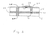
- Figure 3 shows a cross-section of a portion of die 5 after the application of passivation layer 25 over via 20 and bond pad 15.
- atomic layer deposition (ALD) of a suitable dielectric layer such as silicon oxide or thermal oxide is used to ensure pinhole free coverage and because of ALD's ability to control dielectric thickness and related via capacitance.
- an electrically conductive material 30 is then deposited in the vias, using, for instance, chemical vapor deposition (CVD) applied tungsten material to create an electrically conductive path through die 5.
- CVD chemical vapor deposition
- the unique ability to vary the via formation, dielectric application and conductive via fill processes to control via diameter, dielectric thickness and via conductor diameter also allow the formation of various in situ passive components such as capacitors and resistors at and within the via sites and layer.
- predetermined vias 20 and bond pads 15 are exposed through passivation layer 25 on each die 5 on the wafer using conventional photolithographic techniques.
- Conductive metalization interconnects 35 are formed to interconnect desired filled vias and/or bond pads on the die using industry standard techniques
- the inactive surface of the wafer optionally may be back-thinned (not shown) using mechanical or chemical techniques as are well known it the art such as grinding and/or remote atmospheric plasma etching.
- Further testing to identify functional die or die arrays is preferably performed prior to segmenting of the wafer into individual die or die arrays.
- Die 5 are segmented from wafer 1 prior to interconnection and stacking.
- segmented die preferably two to four die, are bonded together with an adhesive 40 and are electrically interconnected at predetermined vias and/or bond pads.
- Alternative preferred embodiments include using a Z-conductive epoxy such as ZTP8090FP available from AI Tech or a solder reflow technique to interconnect top layer vias and bond pads to lower layer bond pads or vias to form "ministacks" of die. If solder is used for interconnection, a suitable epoxy such as Epotek 353 from Epoxy Technology, is used for the bonding of the layers and the stack is reflowed to form the electrical connections.
- a Z conductive epoxy desirably provides both the necessary adhesive and electrical connections for the layers.
- micro-heat pipes may be inserted into the stack where in-stack power dissipation or stack thermal management is a concern.
- a user may selectively process heterogeneous or homogenous integrated circuit die to form modular, scalable, building blocks of circuits.
- each layer may be designed to form a building block of a desired circuit (e.g. op amp, ADC) that, in turn will be assembled into a final circuit of desired complexity.
- the ministack formed at this step may result in the final, desired circuit.
- a further alternative preferred embodiment includes circuit design and die layout specifically providing for efficient bond pad and via locations and for the design of partial circuit "unit cell” layers, that can be assembled as layers to form complete circuits where the vias provide all unit cell interconnections necessary to realize full circuit functionality.
- the ministacks can be bonded and electrically interconnected together to form a stacked electronic module of greater circuit density.
Landscapes
- Internal Circuitry In Semiconductor Integrated Circuit Devices (AREA)
Priority Applications (1)
| Application Number | Priority Date | Filing Date | Title |
|---|---|---|---|
| EP04006259A EP1577948A1 (de) | 2004-03-16 | 2004-03-16 | Mikroelektrisches Stapelmodul mit vertikalen Kontaktlöchern |
Applications Claiming Priority (1)
| Application Number | Priority Date | Filing Date | Title |
|---|---|---|---|
| EP04006259A EP1577948A1 (de) | 2004-03-16 | 2004-03-16 | Mikroelektrisches Stapelmodul mit vertikalen Kontaktlöchern |
Publications (1)
| Publication Number | Publication Date |
|---|---|
| EP1577948A1 true EP1577948A1 (de) | 2005-09-21 |
Family
ID=34833613
Family Applications (1)
| Application Number | Title | Priority Date | Filing Date |
|---|---|---|---|
| EP04006259A Withdrawn EP1577948A1 (de) | 2004-03-16 | 2004-03-16 | Mikroelektrisches Stapelmodul mit vertikalen Kontaktlöchern |
Country Status (1)
| Country | Link |
|---|---|
| EP (1) | EP1577948A1 (de) |
Cited By (2)
| Publication number | Priority date | Publication date | Assignee | Title |
|---|---|---|---|---|
| EP1763079A1 (de) * | 2005-09-07 | 2007-03-14 | Irvine Sensors Corporation | Stapelbare Halbleiterchip-Schicht mit vorgefertigten Graben-Durchkontaktierungen |
| US7947601B2 (en) | 2009-03-24 | 2011-05-24 | Micron Technology, Inc. | Semiconductor devices and methods for forming patterned radiation blocking on a semiconductor device |
Citations (4)
| Publication number | Priority date | Publication date | Assignee | Title |
|---|---|---|---|---|
| EP1267401A2 (de) * | 2001-06-14 | 2002-12-18 | Shinko Electric Industries Co. Ltd. | Halbleiter und seine Herstellung |
| US20030085460A1 (en) * | 1996-10-29 | 2003-05-08 | Oleg Siniaguine | Integrated circuits and methods for their fabrication |
| US6566232B1 (en) * | 1999-10-22 | 2003-05-20 | Seiko Epson Corporation | Method of fabricating semiconductor device |
| US6577013B1 (en) * | 2000-09-05 | 2003-06-10 | Amkor Technology, Inc. | Chip size semiconductor packages with stacked dies |
-
2004
- 2004-03-16 EP EP04006259A patent/EP1577948A1/de not_active Withdrawn
Patent Citations (4)
| Publication number | Priority date | Publication date | Assignee | Title |
|---|---|---|---|---|
| US20030085460A1 (en) * | 1996-10-29 | 2003-05-08 | Oleg Siniaguine | Integrated circuits and methods for their fabrication |
| US6566232B1 (en) * | 1999-10-22 | 2003-05-20 | Seiko Epson Corporation | Method of fabricating semiconductor device |
| US6577013B1 (en) * | 2000-09-05 | 2003-06-10 | Amkor Technology, Inc. | Chip size semiconductor packages with stacked dies |
| EP1267401A2 (de) * | 2001-06-14 | 2002-12-18 | Shinko Electric Industries Co. Ltd. | Halbleiter und seine Herstellung |
Cited By (7)
| Publication number | Priority date | Publication date | Assignee | Title |
|---|---|---|---|---|
| EP1763079A1 (de) * | 2005-09-07 | 2007-03-14 | Irvine Sensors Corporation | Stapelbare Halbleiterchip-Schicht mit vorgefertigten Graben-Durchkontaktierungen |
| US7947601B2 (en) | 2009-03-24 | 2011-05-24 | Micron Technology, Inc. | Semiconductor devices and methods for forming patterned radiation blocking on a semiconductor device |
| US8497186B2 (en) | 2009-03-24 | 2013-07-30 | Micron Technology, Inc. | Semiconductor devices and methods for forming patterned radiation blocking on a semiconductor device |
| US9064984B2 (en) | 2009-03-24 | 2015-06-23 | Micron Technology, Inc. | Semiconductor devices and methods for forming patterned radiation blocking on a semiconductor device |
| US9741762B2 (en) | 2009-03-24 | 2017-08-22 | Micron Technology, Inc. | Semiconductor devices and methods for forming patterned radiation blocking on a semiconductor device |
| US10374001B2 (en) | 2009-03-24 | 2019-08-06 | Micron Technology, Inc. | Semiconductor devices and methods for forming patterned radiation blocking on a semiconductor device |
| US10629647B2 (en) | 2009-03-24 | 2020-04-21 | Micron Technology, Inc. | Semiconductor devices and methods for forming patterned radiation blocking on a semiconductor device |
Similar Documents
| Publication | Publication Date | Title |
|---|---|---|
| US6943442B2 (en) | Electronic parts packaging structure having mutually connected electronic parts that are buried in a insulating film | |
| US9793192B2 (en) | Formation of through via before contact processing | |
| US7943473B2 (en) | Minimum cost method for forming high density passive capacitors for replacement of discrete board capacitors using a minimum cost 3D wafer-to-wafer modular integration scheme | |
| CN102157487B (zh) | 用于集成电路的电感器及方法 | |
| US7919844B2 (en) | Tier structure with tier frame having a feedthrough structure | |
| CN1314117C (zh) | 集成电路封装结构及集成电路封装方法 | |
| US20100291735A1 (en) | Stackable semiconductor chip layer comprising prefabricated trench interconnect vias | |
| US6908785B2 (en) | Multi-chip package (MCP) with a conductive bar and method for manufacturing the same | |
| KR20220084107A (ko) | 마이크로전자 디바이스 조립체 및 패키지 및 관련 방법 및 시스템 | |
| US20090296310A1 (en) | Chip capacitor precursors, packaged semiconductors, and assembly method for converting the precursors to capacitors | |
| JP2006522461A (ja) | 3次元デバイスの製造方法 | |
| JP2005093980A (ja) | 積み重ねが可能な層、ミニスタック、および積層型電子モジュール | |
| US20240355803A1 (en) | Semiconductor packages and methods for forming the same | |
| US20110140281A1 (en) | Substrate for electronic device, stack for electronic device, electronic device, and method for manufacturing the same | |
| US9184113B1 (en) | Methods of forming coaxial feedthroughs for 3D integrated circuits | |
| US8907459B2 (en) | Three-dimensional semiconductor integrated circuit device and method of fabricating the same | |
| CN101410972A (zh) | 用于半导体载体的低欧姆衬底通孔互连 | |
| US20040113222A1 (en) | Stacked microelectronic module with vertical interconnect vias | |
| US7067352B1 (en) | Vertical integrated package apparatus and method | |
| EP1577948A1 (de) | Mikroelektrisches Stapelmodul mit vertikalen Kontaktlöchern | |
| TWI832249B (zh) | 電容結構、半導體結構及其製造方法 | |
| EP1763079A1 (de) | Stapelbare Halbleiterchip-Schicht mit vorgefertigten Graben-Durchkontaktierungen | |
| US20240282723A1 (en) | Integrated circuit (ic) package including an inductive device formed in a conductive routing region | |
| US20260005134A1 (en) | Inductor structures in hybrid bonded devices |
Legal Events
| Date | Code | Title | Description |
|---|---|---|---|
| PUAI | Public reference made under article 153(3) epc to a published international application that has entered the european phase |
Free format text: ORIGINAL CODE: 0009012 |
|
| AK | Designated contracting states |
Kind code of ref document: A1 Designated state(s): AT BE BG CH CY CZ DE DK EE ES FI FR GB GR HU IE IT LI LU MC NL PL PT RO SE SI SK TR |
|
| AX | Request for extension of the european patent |
Extension state: AL LT LV MK |
|
| 17P | Request for examination filed |
Effective date: 20060221 |
|
| AKX | Designation fees paid |
Designated state(s): FR GB |
|
| REG | Reference to a national code |
Ref country code: DE Ref legal event code: 8566 |
|
| 17Q | First examination report despatched |
Effective date: 20090720 |
|
| STAA | Information on the status of an ep patent application or granted ep patent |
Free format text: STATUS: THE APPLICATION IS DEEMED TO BE WITHDRAWN |
|
| 18D | Application deemed to be withdrawn |
Effective date: 20091001 |