EP1227516A2 - Thin film semiconductor device, production process and production apparatus - Google Patents
Thin film semiconductor device, production process and production apparatus Download PDFInfo
- Publication number
- EP1227516A2 EP1227516A2 EP01104444A EP01104444A EP1227516A2 EP 1227516 A2 EP1227516 A2 EP 1227516A2 EP 01104444 A EP01104444 A EP 01104444A EP 01104444 A EP01104444 A EP 01104444A EP 1227516 A2 EP1227516 A2 EP 1227516A2
- Authority
- EP
- European Patent Office
- Prior art keywords
- film
- semiconductor
- semiconductor device
- thin film
- channel region
- Prior art date
- Legal status (The legal status is an assumption and is not a legal conclusion. Google has not performed a legal analysis and makes no representation as to the accuracy of the status listed.)
- Withdrawn
Links
Images


Classifications
-
- B—PERFORMING OPERATIONS; TRANSPORTING
- B23—MACHINE TOOLS; METAL-WORKING NOT OTHERWISE PROVIDED FOR
- B23K—SOLDERING OR UNSOLDERING; WELDING; CLADDING OR PLATING BY SOLDERING OR WELDING; CUTTING BY APPLYING HEAT LOCALLY, e.g. FLAME CUTTING; WORKING BY LASER BEAM
- B23K26/00—Working by laser beam, e.g. welding, cutting or boring
- B23K26/02—Positioning or observing the workpiece, e.g. with respect to the point of impact; Aligning, aiming or focusing the laser beam
- B23K26/06—Shaping the laser beam, e.g. by masks or multi-focusing
- B23K26/062—Shaping the laser beam, e.g. by masks or multi-focusing by direct control of the laser beam
- B23K26/0622—Shaping the laser beam, e.g. by masks or multi-focusing by direct control of the laser beam by shaping pulses
-
- H—ELECTRICITY
- H01—ELECTRIC ELEMENTS
- H01L—SEMICONDUCTOR DEVICES NOT COVERED BY CLASS H10
- H01L21/00—Processes or apparatus adapted for the manufacture or treatment of semiconductor or solid state devices or of parts thereof
- H01L21/02—Manufacture or treatment of semiconductor devices or of parts thereof
- H01L21/02104—Forming layers
- H01L21/02365—Forming inorganic semiconducting materials on a substrate
- H01L21/02656—Special treatments
- H01L21/02664—Aftertreatments
- H01L21/02667—Crystallisation or recrystallisation of non-monocrystalline semiconductor materials, e.g. regrowth
- H01L21/02675—Crystallisation or recrystallisation of non-monocrystalline semiconductor materials, e.g. regrowth using laser beams
- H01L21/02686—Pulsed laser beam
-
- H—ELECTRICITY
- H10—SEMICONDUCTOR DEVICES; ELECTRIC SOLID-STATE DEVICES NOT OTHERWISE PROVIDED FOR
- H10D—INORGANIC ELECTRIC SEMICONDUCTOR DEVICES
- H10D30/00—Field-effect transistors [FET]
- H10D30/60—Insulated-gate field-effect transistors [IGFET]
- H10D30/67—Thin-film transistors [TFT]
- H10D30/6729—Thin-film transistors [TFT] characterised by the electrodes
- H10D30/673—Thin-film transistors [TFT] characterised by the electrodes characterised by the shapes, relative sizes or dispositions of the gate electrodes
- H10D30/6731—Top-gate only TFTs
-
- H—ELECTRICITY
- H10—SEMICONDUCTOR DEVICES; ELECTRIC SOLID-STATE DEVICES NOT OTHERWISE PROVIDED FOR
- H10D—INORGANIC ELECTRIC SEMICONDUCTOR DEVICES
- H10D30/00—Field-effect transistors [FET]
- H10D30/60—Insulated-gate field-effect transistors [IGFET]
- H10D30/67—Thin-film transistors [TFT]
- H10D30/674—Thin-film transistors [TFT] characterised by the active materials
- H10D30/6741—Group IV materials, e.g. germanium or silicon carbide
- H10D30/6743—Silicon
- H10D30/6745—Polycrystalline or microcrystalline silicon
-
- H—ELECTRICITY
- H10—SEMICONDUCTOR DEVICES; ELECTRIC SOLID-STATE DEVICES NOT OTHERWISE PROVIDED FOR
- H10D—INORGANIC ELECTRIC SEMICONDUCTOR DEVICES
- H10D62/00—Semiconductor bodies, or regions thereof, of devices having potential barriers
- H10D62/40—Crystalline structures
-
- H—ELECTRICITY
- H10—SEMICONDUCTOR DEVICES; ELECTRIC SOLID-STATE DEVICES NOT OTHERWISE PROVIDED FOR
- H10D—INORGANIC ELECTRIC SEMICONDUCTOR DEVICES
- H10D86/00—Integrated devices formed in or on insulating or conducting substrates, e.g. formed in silicon-on-insulator [SOI] substrates or on stainless steel or glass substrates
- H10D86/01—Manufacture or treatment
- H10D86/021—Manufacture or treatment of multiple TFTs
- H10D86/0221—Manufacture or treatment of multiple TFTs comprising manufacture, treatment or patterning of TFT semiconductor bodies
- H10D86/0223—Manufacture or treatment of multiple TFTs comprising manufacture, treatment or patterning of TFT semiconductor bodies comprising crystallisation of amorphous, microcrystalline or polycrystalline semiconductor materials
- H10D86/0227—Manufacture or treatment of multiple TFTs comprising manufacture, treatment or patterning of TFT semiconductor bodies comprising crystallisation of amorphous, microcrystalline or polycrystalline semiconductor materials using structural arrangements to control crystal growth, e.g. placement of grain filters
-
- H—ELECTRICITY
- H10—SEMICONDUCTOR DEVICES; ELECTRIC SOLID-STATE DEVICES NOT OTHERWISE PROVIDED FOR
- H10D—INORGANIC ELECTRIC SEMICONDUCTOR DEVICES
- H10D86/00—Integrated devices formed in or on insulating or conducting substrates, e.g. formed in silicon-on-insulator [SOI] substrates or on stainless steel or glass substrates
- H10D86/01—Manufacture or treatment
- H10D86/021—Manufacture or treatment of multiple TFTs
- H10D86/0221—Manufacture or treatment of multiple TFTs comprising manufacture, treatment or patterning of TFT semiconductor bodies
- H10D86/0223—Manufacture or treatment of multiple TFTs comprising manufacture, treatment or patterning of TFT semiconductor bodies comprising crystallisation of amorphous, microcrystalline or polycrystalline semiconductor materials
- H10D86/0229—Manufacture or treatment of multiple TFTs comprising manufacture, treatment or patterning of TFT semiconductor bodies comprising crystallisation of amorphous, microcrystalline or polycrystalline semiconductor materials characterised by control of the annealing or irradiation parameters
-
- H—ELECTRICITY
- H10—SEMICONDUCTOR DEVICES; ELECTRIC SOLID-STATE DEVICES NOT OTHERWISE PROVIDED FOR
- H10D—INORGANIC ELECTRIC SEMICONDUCTOR DEVICES
- H10D86/00—Integrated devices formed in or on insulating or conducting substrates, e.g. formed in silicon-on-insulator [SOI] substrates or on stainless steel or glass substrates
- H10D86/01—Manufacture or treatment
- H10D86/021—Manufacture or treatment of multiple TFTs
- H10D86/0251—Manufacture or treatment of multiple TFTs characterised by increasing the uniformity of device parameters
-
- H—ELECTRICITY
- H01—ELECTRIC ELEMENTS
- H01L—SEMICONDUCTOR DEVICES NOT COVERED BY CLASS H10
- H01L21/00—Processes or apparatus adapted for the manufacture or treatment of semiconductor or solid state devices or of parts thereof
- H01L21/02—Manufacture or treatment of semiconductor devices or of parts thereof
- H01L21/02104—Forming layers
- H01L21/02365—Forming inorganic semiconducting materials on a substrate
- H01L21/02656—Special treatments
- H01L21/02664—Aftertreatments
- H01L21/02667—Crystallisation or recrystallisation of non-monocrystalline semiconductor materials, e.g. regrowth
- H01L21/02691—Scanning of a beam
Definitions
- the present invention relates to a thin film semiconductor device having a polycrystalline semiconductor film, and a process and apparatus for producing a polycrystalline semiconductor film.
- the thin film semiconductor device of the present invention is useful for image display devices.
- Fig.12 shows the most general process for crystallizing with an excimer pulse laser of the prior art.
- the whole substrate is crystallized by irradiating a non-crystal silicon film 102 ,which was formed on a substrate 100 through an base film 101, with a laser beam 105 from a linear excimer laser having a width L of several millimeters on the substrate and moving the laser exposure position at intervals of 1 to several pulses.
- crystal nuclei are formed at random upon laser exposure.
- the average distance between the formed crystal nuclei is 0.5 ⁇ m or less under ordinary laser annealing conditions. Therefore, the obtained polycrystalline silicon film 103 has a grain size of 0.5 ⁇ m or less and is not uniform in size.
- an international patent publication WO9745827 discloses the following process. That is, when the width L of the laser beam 105 shown in Fig.12 is reduced to 0.5 ⁇ m or less and the position of the laser beam 105 having this shape is moved 0.5 ⁇ m or less each time to irradiate pulses, crystal grows in one direction with the initially formed crystal grains as seeds.
- the above one direction is a transverse direction, that is, a direction perpendicular to the thickness direction of the grown film.
- the obtained crystals have a grain size of 1 ⁇ m or less and are greatly nonuniform in grain size.
- the orientation of grains is out of order, the density of defects is large, and the roughness of the film surface is large. Therefore, it is impossible to grow polycrystalline silicon having a large grain size or to control the grain size or the position of the grain boundary accurately. Therefore, the grain boundary is included in the channel at random. Consequently, it is difficult to improve the characteristic properties, reliability and uniformity of TFT devices.
- the beam Since the beam must be converged to a size of 1 ⁇ m or less in the technology disclosed by the above international patent publication WO9745827, the energy of the laser is lost and the optical system of an irradiation laser become complicated. As the moving distance between laser pulses is 1 ⁇ m or less, it takes a long time to crystallize the whole substrate and it is difficult to improve throughput and reduce costs. Particularly, this process cannot be applied to a large-area substrate. Further, very small distance movement is easily influenced by vibration and involves a yield problem.
- a thin film semiconductor device which has an insulating substrate, a first semiconductor film which is a polycrystalline semiconductor film, a gate electrode formed on the first semiconductor film through a gate. insulating film, first charge transmitting and receiving means and second charge transmitting and receiving means formed on the first semiconductor film at a predetermined interval therebetween, and a channel region formed between the first and second charge transmitting and receiving means, wherein the main orientation of the first semiconductor film constituting the channel region is ⁇ 110 ⁇ with respect to the main surface of the insulating substrate or the gate insulating film.
- An MIS type thin film semiconductor device may vary in structure as follows.
- a thin film semiconductor device which has an insulating substrate, a first semiconductor film which is a polycrystalline semiconductor film, a gate electrode formed on the first semiconductor film through a gate insulating film, first charge transmitting and receiving mean and second charge transmitting and receiving means formed on the first semiconductor film at a predetermined interval therebetween, and a channel region formed between the first and second charge transmitting and receiving means, wherein the main orientation of the first semiconductor film constituting the channel region is ⁇ 110 ⁇ with respect to the main surface of the insulating substrate or the gate insulating film; and the first semiconductor film is essentially composed of crystal grains having an axis in a longitudinal direction of 45° or less with respect to a direction for connecting the first and second charge transmitting and receiving means in the channel region.
- This thin film semiconductor device is a more practical embodiment of the present invention.
- the first semiconductor film comprises a small inclination grain boundary having an angle of 75° or less with respect to a direction for connecting the first and second charge transmitting and receiving means.
- a thin film semiconductor device which has an insulating substrate, a first semiconductor film which is a polycrystalline semiconductor film, a gate electrode formed on the first semiconductor film through a gate insulating film, first charge transmitting and receiving mean and second charge transmitting and receiving means formed on the first semiconductor film at a predetermined interval therebetween, and a channel region formed between the first and second charge transmitting and receiving means, wherein the main orientation of the first semiconductor film constituting the channel region is ⁇ 110 ⁇ with respect to the main surface of the insulating substrate or the gate insulating film; and the channel region of the first semiconductor film has crystal grains for connecting the first charge transmitting and receiving means and the second charge transmitting and receiving means.
- the third aspect of the present invention is more preferred. That is, the channel region of the first semiconductor film is composed of crystal grains having such a length in a longitudinal direction as to connect the first charge transmitting and receiving means and the second charge transmitting and receiving means. Therefore, a thin film semiconductor device having higher reliability can be provided.
- a thin film semiconductor device which has an insulating substrate, a first semiconductor film which is a polycrystalline semiconductor film, a gate electrode formed on the first semiconductor film through a gate insulating film, first charge transmitting and receiving mean and second charge transmitting and receiving means formed on the first semiconductor film at a predetermined interval therebetween, and a channel region formed between the first and second charge transmitting and receiving means, wherein the main orientation of the first semiconductor film constituting the channel region is ⁇ 110 ⁇ with respect to the main surface of the insulating substrate or the gate insulating film; and the main orientation of the surface of the first semiconductor film substantially perpendicular to a direction for connecting the first and second charge transmitting and receiving means is ⁇ 100 ⁇ .
- the channel region of the first semiconductor film is composed of crystal grains having a length in a longitudinal direction for connecting the first charge transmitting and receiving means and the second charge transmitting and receiving means, and the main orientation of the polycrystalline film is ⁇ 100 ⁇ , thereby making it possible to provide a thin film semiconductor device having extremely high reliability.
- each crystal grain has the same properties as a monocrystal though the first semiconductor film is polycrystal.
- a thin film semiconductor device which has at least two semiconductor device portions on an insulating substrate, a second semiconductor layer and an insulating film layer selectively formed on a partial region of the insulating substrate, the laminate consisting of the second semiconductor layer and the insulating film layer being in contact with a first semiconductor layer, the second semiconductor layer being not existent between a first semiconductor device and a second semiconductor device, a gate electrode formed on the first semiconductor layer through a gate insulating film, first charge transmitting and receiving means and second charge transmitting and receiving means formed on the first semiconductor film at a predetermined interval therebetween, and a channel region formed between the first and second charge transmitting and receiving means.
- the main orientation of the first semiconductor film constituting the channel region is more preferably ⁇ 110 ⁇ with respect to the main surface of the insulating non-crystalline substrate or the gate insulating film.
- This thin film semiconductor device has the second semiconductor layer below a desired semiconductor device portion and the semiconductor device portion has the first aspect of the present invention. Further, in the present invention, the second semiconductor layer may be existent below the desired semiconductor device portion and the semiconductor device portion may have any one of the second to fourth aspects of the present invention. It is needless to say that the present invention can be carried out using any one of the semiconductor device portions disclosed in this specification.
- a thin film semiconductor device which has at least two semiconductor device portions on an insulating substrate, a second thin film which is selectively formed on a first thin film having a first heat conductivity and which has a second heat conductivity higher than the first heat conductivity, the second thin film being not in contact with a semiconductor layer and arranged between a first semiconductor device portion and a second semiconductor device portion, and the semiconductor device portions being the thin film semiconductor device of any one of the first to fourth aspects of the present invention.
- a thin film semiconductor device which has at least two semiconductor device portions on an insulating substrate, a second thin film which is selectively formed on a first thin film having a first heat conductivity and which has a second heat conductivity lower than the first heat conductivity, the second thin film being in contact with a semiconductor layer and not arranged between a first semiconductor device portion and a second semiconductor device portion, and the semiconductor device portions being the thin film semiconductor device of any one of the first to fourth aspects.
- a semiconductor film production process according to the major aspects of the present invention will be described hereinbelow.
- a polycrystalline semiconductor film of interest can be obtained by using the following process.
- a process for producing a polycrystalline semiconductor film by carrying out separately the step of growing crystal nuclei in a semiconductor layer formed on an insulating substrate and the step of melt recrystallizing a semiconductor thin film by irradiating a laser beam to grow crystal grains.
- a process for producing a polycrystalline semiconductor film wherein a non-crystalline semiconductor film formed on the insulating substrate is melt recrystallized by irradiating a laser beam to grow crystal grains.
- a process for producing a polycrystalline semiconductor film wherein the wavelength of the laser beam is selected from a range of 240 nm to 600 nm and the absorption coefficient for the wavelength of the non-crystalline semiconductor film is larger than the absorption coefficient of the polycrystalline semiconductor film.
- a process for producing a polycrystalline semiconductor film wherein the crystal nuclei of the polycrystalline silicon film formed on the insulating film are formed by melt recrystallization by the irradiation of a laser beam.
- the crystal nuclei of the polycrystalline silicon film on the insulating substrate are preferably grown by catalytic chemical vapor deposition.
- the production apparatus of the present invention comprises means for modulating the pulse width of a laser beam, the time-dependent shape of laser beam intensity and the interval of laser beam pulses, means for shaping the irradiation range of the profile of the laser beam irradiated from an oscillation source to a predetermined form and focusing it on an object to be irradiated, and means of moving the insulating substrate at a predetermined speed and pitch in synchronism with the irradiation of the laser beam.
- the charge transmitting and receiving means generally means a source or drain region.
- a region thicker than the channel region is formed in part of a drain or source region constituting a semiconductor layer. Thereby, an extremely useful polycrystalline semiconductor film can be obtained.
- the pulse width of the above laser beam is 100 ns to 1 ms and the energy density is 200 mJ/cm 2 to 10 J/cm 2 .
- the intensity distribution of the laser beam has such a distribution pattern that intensity is uniform in the width of the beam, or monotonously increases or decreases from one direction to the other.
- an MIS type field effect transistor having a gate electrode formed on a first semiconductor layer which is a polycrystalline semiconductor film formed on an insulating substrate through a gate insulating film, a channel region formed on the semiconductor layer and a source region and a drain region formed on both sides of the channel region, wherein a semiconductor layer which is a polycrystalline semiconductor film used in the channel of a semiconductor in which the main orientation of crystal grains constituting the channel region with respect to the surface of the substrate or the gate insulating film is ⁇ 110 ⁇ and the main orientation of the surface perpendicular to a direction for connecting the source and drain regions is ⁇ 100 ⁇ .
- the first feature is that a small inclination angle grain boundary having an angle of 75° or less is located between the source and drain regions of the channel region.
- the second feature is that the surface roughness of the channel region is smaller than 20 nm and the internal tensile stress of the channel region is 10 9 dyn/cm 2 or more.
- the third feature is that the density of metal elements contained in the semiconductor layer is 10 19 cm -3 or less and the density of crystal defects contained in the channel region is 10 17 cm -3 or less.
- a preferred example of the thin film semiconductor device. of the present invention is a thin film semiconductor device which has a low-melting point glass substrate as the above insulating substrate.
- the insulating substrate is typified by a non-crystalline substrate such as a glass substrate, particularly a low-melting point glass substrate.
- the present invention provides the following thin film semiconductor devices:
- the grain size of the semiconductor crystals of the channel region may be larger than the grain size of the crystal grains of the charge transmitting and receiving means, that is, source and drain regions.
- the present invention also provides the following polycrystalline semiconductor thin film production processes:
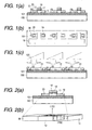
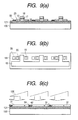
- Figs. 1(a) to 1(c) are diagrams for explaining a thin film semiconductor device according to Embodiment 1 of the present invention.
- Figs. 1(a) to 1(c) show the thin film semiconductor device having three polycrystalline silicon thin film transistors.
- Fig. 1(a) is a sectional view and
- Fig. 1(b) is a plan view of the thin film semiconductor device.
- reference numeral 100 denotes an insulating substrate, 101 underlying layer film, 18 gate electrode and 17 gate insulating film.
- a glass substrate is frequently used as the insulating substrate.
- a silicon dioxide (SiO 2 ) film is generally used as the above underlying layer film.
- Each silicon semiconductor layer comprises a channel region 12, a source region 20, a drain region 19 and a projecting crystal nucleus region 30.
- the channel region 12 is composed of a polycrystalline silicon film having a large grain size and the crystal nucleus region 30 is generally composed of a polycrystalline silicon film having a small grain size.
- the gate electrodes 18 are connected to one another.
- the gate electrode may be formed independently.
- the channel region 12 having a large grain size is obtained by a crystallization method as shown in Fig. 1(c).
- An amorphous silicon film or polycrystalline silicon film is irradiated with an inclined linear laser beam having an intensity distribution as shown in Fig. 1(c).
- Reference numeral 105 in Fig. 1(c) denotes a typical inclined intensity distribution of this laser light.
- the pulse width of the laser light is desirably selected from a range of 100 ns to 1 ms.
- the optimum laser conditions for obtaining a silicon semiconductor layer film having a thickness of 300 nm or less and a grain size of for example 5 ⁇ m which is larger than the length of the channel are a pulse width of 10 ms and a power of 1 w.
- crystallization starts from the crystal nucleus region 30 where the silicon film is thicker than the silicon film therearound. That is, crystal growth begins from a low-temperature region. Crystals grow in a direction shown by arrows in Fig. 1(c) and a polycrystalline silicon film 31 having a larger grain size than the channel region is formed.
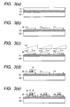
- Figs. 3(a) to 3(e) are sectional views showing the production process of the thin film semiconductor device of this embodiment.
- a base layer which is a silicon dioxide film 101 and an amorphous or polycrystalline silicon film 110 are formed on a non-crystalline substrate 100 made from glass or the like (Fig. 3(a)).
- This amorphous silicon film or polycrystalline silicon film 110 is processed into three regions by etching using a general photoresist. At this point, the crystal nucleus region 30 is formed (Fig. 3(b)).
- the thus prepared substrate is irradiated with laser light having the above-mentioned inclined luminous or light intensity (Fig. 3(c)). In this case, laser light is adjusted to have inclined luminous intensity according to the region of each semiconductor device.
- the gate insulating film 17 and the gate electrode 18 are formed (Fig. 3(d)).
- a source and drain are formed by general ion implantation. Impurities such as phosphorus and boron are frequently used (Fig. 3(e)).
- the step of melt recrystallizing the semiconductor thin film by the irradiation of a laser beam to grow grains from the above crystal nuclei can be carried out separately.
- the wavelength of a laser beam suitable to selectively grow crystal grains efficiently is desirably selected from a range of 240 to 600 nm.
- the reason for this is that the absorption coefficient of the amorphous silicon film at a wavelength of 500 nm is about 5 times larger than the absorption coefficient of the polycrystalline silicon film. Therefore, it is easy to selectively melt recrystallize other semiconductor layer regions with crystal nuclei composed of a polycrystalline silicon film as a seed.
- the crystal nucleus region composed of a polycrystalline silicon film having a small grain size on the insulating substrate can be formed by melt recrystallization with the irradiation of a general excimer pulse.laser beam.
- Figs. 2(a) and 2(b) schematically show the crystalline state of the semiconductor layer, particularly the channel region.
- Fig. 2(a) is a sectional view of one transistor portion and.
- Fig. 2(b) is a perspective view of the semiconductor layer.
- the corresponding region in Fig. 2(a) and Fig. 2(b) is shown by dotted lines.
- the same reference numerals denote the same elements as in Figs. 1(a) to 1(c). This embodiment is the most preferred embodiment of the present invention.
- the main orientation of a polycrystalline substance at least in the channel region 12 is ⁇ 110 ⁇ with respect to the surface of the gate insulating film and the substrate.
- the polycrystalline substance is a polycrystalline silicon film having a main orientation of the surface almost perpendicular to a direction for connecting the source region 20 and the drain region 19 such as of ⁇ 100 ⁇ .
- a small inclination angle grain boundary having a rotation angle of 70° or less is located between a plurality of crystal grains constituting the channel region 12.
- the surface roughness of the channel region 12 is smaller than 20 nm, the internal tensile stress is 10 9 dyn/cm 2 or more, and the density of the contained crystal defects is 10 17 cm -3 or less.
- the density of metal elements contained in the whole semiconductor layer including the channel region 12 is 10 19 cm -3 or less.
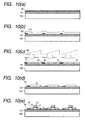
- Fig. 4 shows an example of production apparatus used in the embodiment of the present invention.
- This apparatus is suitable for the formation of a polycrystalline semiconductor film by melt recrystallizing a semiconductor thin film by irradiating the non-crystalline or polycrystalline semiconductor thin film formed on the insulating substrate 205 shown in Figs. 2(a) and 2(b) with a laser beam.
- This apparatus has a CW laser unit 200, means of modulating the pulse width, time-dependent shape and interval of the laser beam (201, 202, 203), optical system for focusing a laser beam from an oscillation source and moving means capable of moving the laser beam relative to an object to be irradiated.
- the modulation means has an EO modulator 201, polarizing plate 202 and driver 203.
- the optical system comprises a beam shaping unit 204 for shaping the profile of the laser beam irradiated from the oscillation source to an appropriate form by means of an optical system consisting of a plurality of lenses or diffraction optical element, a mirror 208 having a scanning function and focusing lens system 207 for focusing the laser beam.
- the moving means is capable of moving the insulating substrate 205 at a predetermined pitch in synchronism with the irradiation of the laser beam.
- Fig. 5(a) and Fig. 5(b) show the pulse width, time-dependent shape and pulse interval of the laser beam.
- Fig. 5(a) shows the waveform of voltage applied to the EO modulator 201
- Fig. 5(b) shows the waveform of beam intensity through a polarizer.
- the rise time, pulse width, fall time and pulse interval of beam intensity can be controlled by voltage from the outside.
- Figs. 5(a) and 5(b) show two pulses having different widths and an inclined pulse to be controlled..
- Fig. 6(a) and Fig. 6(b) show the shapes of laser beams. These perspective views show the shapes of a laser beam which has been shaped to a desired form by the beam shaping unit 204 and focused on a sample by the focusing lens.
- Fig. 6(a) shows a distribution pattern that intensity monotonously increases from one direction to the other and
- Fig. 6(b) shows uniform intens ity in the width of a beam.
- a desired region can be crystallized.
- the alignment pattern on the insulating substrate can be detected by a level difference of the semiconductor layer film or a level difference in the crystal nucleus region 30 in Figs. 1(a) to 1(c). Stated more specifically, the laser beam can be aligned with the substrate by an interferometer.
- a high-quality polycrystalline semiconductor film whose grain boundary, grain size and crystallization direction can be controlled and whose film roughness and crystal defects formed by crystallization have been reduced can be formed on the insulating substrate made from glass or the like.
- a production process and apparatus for forming a low-cost and high-quality polycrystalline semiconductor film, which can reduce the number of production steps, can be applied to a large-area substrate, and have a high throughput are realized.
- the field effect mobility can be controlled to about 300 cm 2 /V ⁇ s or more and variations in threshold voltage can be suppressed to ⁇ 0.2 V or less.
- a thin film semiconductor device which operates with high performance and high reliability and has excellent uniformity among devices can be obtained.
- a polycrystalline silicon film is used as a semiconductor film before the irradiation of a laser beam.
- an amorphous silicon film is used, the same effect is obtained.
- an inclined laser beam is used.
- a uniform beam is used, the same effect is obtained.
- crystals are grown with the crystal nucleus region 30 as a starting point. By optimizing the shape of a laser beam, the same effect is obtained in a structure containing no crystal nuclei 30 on the projection.
- the initial semiconductor film is a polycrystalline silicon film containing crystal nuclei and can be obtained by melt recrystallization by the irradiation of an excimer laser beam. The same effect is obtained when the above polycrystalline silicon film is formed at a low temperature by CAT-CVD (Catalytic-Chemical Vapor Deposition).
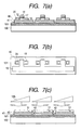
- Figs. 7(a) to 7(c) are diagrams for explaining a semiconductor device according to Embodiment 2 of the present invention.
- a second semiconductor layer is formed below the semiconductor layer constituting a channel from the viewpoint of crystal growth.
- Figs. 7(a) to 7(c) show three polycrystalline silicon thin film transistors mounted.
- Fig. 7(a) is a sectional view and
- Fig. 7(b) is a plan view of the semiconductor device.
- Fig. 7(c) is a sectional view for explaining a laser beam irradiation method.
- reference numeral 100 denotes an insulating substrate, 101 underlying layer film, 18 gate electrode and 17 gate insulating film.
- a glass substrate is frequently used as the insulating substrate.
- a silicon dioxide film is generally used as the underlying layer film.
- the first semiconductor layer has a channel region 12, source region 20 and drain region 19.
- the channel.region 12 is composed of a polycrystalline silicon film having a large grain size.
- a second semiconductor layer 41 is selectively inserted between the silicon semiconductor layer and the underlying layer film 101 with an insulating film 40. The second semiconductor layer 41 is not formed in a region between a plurality of semiconductor devices.
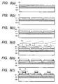
- Figs. 8(a) to 8(f) are sectional views showing a process for producing the thin film semiconductor device of this embodiment.
- a base layer which is the silicon dioxide film 101, an amorphous silicon layer which is the second semiconductor layer 41 and a silicon dioxide layer 40 are formed on a non-crystalline substrate 100 made from glass or the like (Fig. 8(a)).
- the above layers 40 and 41 are processed into three regions of predetermined thin film semiconductor devices by etching (Fig. 8(b)).
- An amorphous silicon film or polycrystalline silicon film 110 is formed on the above layers (Fig. 8(c)).
- the thus prepared substrate is irradiated with laser light 105 having the above-mentioned inclined luminous intensity (Fig. 8(d)).
- a region devoid of the second semiconductor film 40 is a crystal nucleus region.
- the gate insulating film 17 and the gate electrode 18 are formed on the first semiconductor. thin film. A source and a drain are formed by a commonly used method (Fig. 8(f)).
- the channel region 12 having a large grain size is obtained by a crystallization method shown in Fig. 7(c).
- the amorphous silicon film or polycrystalline silicon film is irradiated with an inclined linear laser beam having an intensity distribution shown in Fig. 7(c).
- the pulse width of the laser is desirably selected from a range of 100 ns to 1 ms.
- the optimum laser conditions for obtaining a silicon semiconductor layer film having thickness of 100 nm or less and a grain size of 5 ⁇ m which is larger than the length of the channel are a pulse width of 10 ms and a power of 1 w.
- crystallization starts from a region devoid of the second silicon semiconductor layer below the silicon semiconductor layer.
- the reason for this is that the laser beam passing through the first silicon semiconductor film reaches the second silicon semiconductor film when the laser beam is irradiated.
- the laser beam is absorbed in the second silicon semiconductor film and the temperature of the semiconductor layer rises.
- This temperature rise functions as a heat sink to suppress quenching.
- this heat sink is not formed in the layer underlying the first silicon semiconductor layer, the temperature is low and the crystallization start time is early. Therefore, crystallization starts from the region devoid of the second semiconductor layer below the first silicon semiconductor layer and the region becomes the crystal nucleus region 42..
- the wavelength of a laser beam suitable for selectively growing crystal grains at a high efficiency is desirably selected from a range of 240 to 600 nm.
- the step of melt recrystallizing the semiconductor thin film by the irradiation of a laser beam to grow grains from the crystal nuclei can be carried out separately.
- the crystal nucleus region composed of a polycrystalline silicon film having a small grain size on the insulating substrate can be formed by melt recrystallization with the irradiation of a laser beam from an excimer pulse laser of the prior art.
- Figs. 2(a) and 2(b) show the crystal state of the semiconductor layer, particularly the channel region.
- the semiconductor layer is composed of a polycrystalline silicon film in which at least the main orientation of the channel region is ⁇ 110 ⁇ with respect to the surface of the gate insulating film and the main orientation of the surface almost perpendicular to a direction for connecting the above source region 20 and the drain region 19 is ⁇ 100 ⁇ .
- a small inclination angle grain boundary having a rotation angle of 75° or less is formed between a plurality of crystal grains constituting the channel region 12.
- the surface roughness of the channel region 12 is smaller than 20 nm, the internal tensile stress thereof is 10 9 dyn/cm 2 or more, and the density of crystal defects contained therein is 10 17 cm -3 or less.
- the density of metal elements contained in the whole semiconductor layer including the channel region 12 is 10 19 cm -3 or less.
- the alignment pattern on the insulating substrate can be detected by a level difference between the second semiconductor layer film 41 and the insulating film 40 or a level difference in the crystal nucleus region 42 in Fig. 8.
- a high-quality polycrystalline semiconductor film whose grain boundary, grain size and crystal orientation can be controlled and whose film roughness and crystal defects formed by crystallization have been reduced can be formed on the insulating substrate made from glass or the like.
- a production process and apparatus for forming a low-cost and high-quality polycrystalline semiconductor film, which can reduce the number of production steps, can be applied to a large-area substrate, and have a high throughput are realized.
- the field effect . mobility can be controlled to be about 300 cm 2 /V ⁇ s or more and variations in threshold voltage can be suppressed to ⁇ 0.2 V or less.
- a semiconductor device which operates with high performance and high reliability and is excellent in uniformity among devices can be obtained.
- Figs. 9(a) to 9(c) are diagrams for explaining a semiconductor device according to Embodiment 3 of the present invention.
- a member which facilitates the partial radiation of heat during crystal growth is used.
- Figs. 9(a) to 9(c) show a semiconductor device having three polycrystalline silicon thin film transistors formed thereon.
- Fig. 9(a) is a sectional view and
- Fig. 9(b) is a plan view of the semiconductor device.
- reference numeral 100 denotes an insulating substrate, 101 underlying layer film, 19 gate electrode and 17 gate insulating film.
- the semiconductor layer is composed of a channel region 12, source region 20 and drain region 19, and the channel region 12 is composed of a polycrystalline silicon film having a large grain size.
- An insulating film 50 is selectively formed on the underlying layer film 101 between a plurality of semiconductor devices. The heat conductivity of the insulating film 50 is higher than the heat conductivity of the underlying layer film 101 and the insulating substrate 100.
- Figs. 10(a) to 10(e) are sectional views showing the production process of the thin film semiconductor device of this embodiment.
- a base layer which is a silicon dioxide film 101 and a Si 3 N 4 layer as the insulating film 50 having a higher heat conductivity than the underlying layer film 101 are formed on the non-crystalline substrate 100 made from glass or the like (Fig. 10(a)).
- This insulating film 50 provide is for the area of each thin film semiconductor device.
- the region where this insulating film 50 is provided is a crystal nucleus region.
- An amorphous silicon film or polycrystalline silicon film 110 is formed on the thus prepared substrate (Fig. 10(b)).
- the thus prepared substrate is irradiated with laser light 105 having the above inclined luminous intensity (Fig. 10(c)).
- the first semiconductor thin film is processed to a desired shape (Fig. 10(d)).
- the gate insulating film 17 and the gate electrode 18 are formed on this first semiconductor thin film.
- a source and a drain are formed by a general method (Fig. 10(e)).
- the channel region 12 having a large grain size is obtained by a crystallization method shown in Fig. 9(c).
- the amorphous silicon film or polycrystalline silicon film is irradiated with an inclined linear laser beam having an intensity distribution shown in Fig. 9(c).
- the pulse width of the laser is desirably selected from a range of 100 ns to 1 ms.
- the optimum laser conditions.for obtaining a silicon semiconductor layer film having thickness of 100 nm or less and a grain size of 5 ⁇ m which is larger than the length of the channel are a pulse width of 10 ⁇ s and a power of 1 w.
- the semiconductor region having the insulating film 50 therebeneath has a larger amount of heat dissipated downward than other semiconductor film regions as the heat conductivity of the insulating film 50 is higher than the heat conductivity of the amorphous silicon film or polycrystalline silicon film 110 with the result that that semiconductor region becomes a crystal nucleus region due to an early reduction in temperature and an early crystallization start time.
- the step of melt recrystallizing the semiconductor thin film by irradiating a laser beam to grow grains from the crystal nuclei can be carried out separately.
- the crystal nucleus region composed of a polycrystalline silicon film having a small grain size on the insulating substrate can be formed by melt recrystallization by the irradiation of a laser beam from an excimer pulse laser of the prior art.
- the insulating film 50 is processed to a rectangular shape.
- a silicon nitride film is suitable for use as the insulating film 50.
- Figs. 2(a) and 2(b) show the crystal state of the semiconductor layer, particularly the channel region.
- the semiconductor layer is composed of a polycrystalline silicon film in which at least the main orientation of the channel region is ⁇ 110 ⁇ with respect to the surface of the gate insulating film and the main orientation of the surface almost perpendicular to a direction for connecting the above source region 20 and the drain region 19 is ⁇ 100 ⁇ .
- a small inclination angle grain boundary having a rotation angle of 70° or less is formed between a plurality of crystal grains constituting the channel region 12.
- the surface roughness of the channel region 12 is smaller than 20 nm, the internal tensile stress thereof is 10 9 dyn/cm 2 or more, the density of crystal defects contained therein is 10 17 m -3 or less, and the density of metal elements contained in the whole semiconductor layer including the channel region 12 is 10 19 cm -3 or less.
- the alignment pattern on the insulating substrate can be detected by the level difference of the insulating film 51 in Figs. 11(a) to 11(c).
- a high-quality polycrystalline semiconductor film whose grain boundary, grain size and crystal orientation can be controlled and whose film roughness and crystal defects formed by crystallization have been reduced can be formed on the insulating substrate made from glass or the like.
- a production process and apparatus for forming a low-cost and high-quality polycrystalline semiconductor film, which can reduce the number of production steps, can be applied to a large-area substrate, and have a high throughput are realized.
- the field effect mobility can be controlled to be about 300 cm 2 /V ⁇ s or more, variations in threshold voltage can be suppressed to ⁇ 0.2 V or less, and a semiconductor device which operates with high performance and high reliability and is excellent in uniformity among devices can be obtained.
- Figs. 11(a) to 11(c) are diagrams for explaining a semiconductor device according to Embodiment 4 of the present invention.
- Fig. 11 (a) is a sectional view of a semiconductor device having three polycrystalline silicon thin film transistors formed thereon and
- Fig. 11(b) is a plan view thereof.
- reference numeral 100 denotes an insulating substrate, 101 underlying layer film, 51 insulating film, 18 gate electrode and 17 gate insulating film.
- the semiconductor layer comprises a channel region 12, source region 20 and drain region 19, and the channel region 12 is composed of a polycrystalline silicon film having a large grain size.
- the insulating film 51 is selectively inserted between the silicon semiconductor layer and the underlying layer film 101.
- the heat conductivity of the insulating film 51 is made lower than the heat conductivity of the amorphous silicon film or polycrystalline silicon film 31.
- the channel region 12 having a large grain size is obtained by a crystallization method shown in Fig. 11(c).
- the amorphous silicon film or polycrystalline silicon film is irradiated with an inclined linear laser beam having an intensity distribution shown in Fig. 11(c).
- the pulse width of the laser is desirably selected from a range of 100 ns to 1 ms.
- the optimum laser conditions for obtaining a silicon semiconductor layer film having thickness of 100 nm or less and a grain size of 5 ⁇ m which is larger than the length of the channel are a pulse width of 10 ⁇ s and a power of 1 w.
- crystallization starts from a region where the insulating film 51 is not formed below the silicon semiconductor layer.
- the semiconductor region having the insulating film 51 therebeneath has a smaller amount of heat dissipated downward than other semiconductor film regions as the heat conductivity of the insulating film 51 is lower than the heat conductivity of the amorphous silicon film or polycrystalline silicon film 31 with the result that that semiconductor region becomes a crystal nucleus region 42 due to an early reduction in temperature and an early crystallization start time.
- the step of melt recrystallizing the semiconductor thin film by irradiating a laser beam to grow grains from the crystal nuclei can be carried out separately.
- the crystal nucleus region composed of a polycrystalline silicon film having a small grain size on the insulating substrate can be formed by melt recrystallization by the irradiation of a laser beam from an excimer pulse laser of the prior art.
- An insulating film having a small density and a small dielectric constant or a porous silicon oxide film is suitable for use as the insulating film 51.
- Figs. 2(a) and 2(b) show the crystal state of the semiconductor layer, particularly the channel region.
- the semiconductor layer is composed of a polycrystalline silicon film in which at least the main orientation of the channel region is ⁇ 110 ⁇ with respect to the surface of the gate insulating film . and the main orientation of the surface almost perpendicular to a direction for connecting the above source region 20 and the drain region 19 is ⁇ 100 ⁇ .
- a small inclination angle grain boundary having a rotation angle of 70° or less is. formed between a plurality of crystal grains constituting the channel region 12.
- the surface roughness of the channel region 12 is smaller than 20 nm, the internal tensile stress thereof is 10 9 dyn/cm -2 or more, the density of crystal defects contained therein is 10 17 m -3 or less, and the density of metal elements contained in the whole semiconductor layer including the channel region 12 is 10 19 cm -3 or less.
- the alignment pattern on the insulating substrate can be detected by the level difference of the insulating film 50 in Figs. 11(a) to 11(c).
- a high-quality polycrystalline semiconductor film whose grain boundary, grain size and crystal orientation can be controlled and whose film roughness and crystal defects formed by crystallization have been reduced can be formed on the insulating substrate made from glass or the like.
- a production process and apparatus for forming a low-cost and high-quality polycrystalline semiconductor film, which can reduce the number of production steps, can be applied to a large-area substrate, and have a high throughput are realized.
- the field effect mobility can be controlled to be about 300 cm 2 /V ⁇ s or more, variations in threshold voltage can be suppressed to ⁇ 0.2 V or less, and a semiconductor device which operates with high performance and high reliability and is excellent in uniformity among devices can be obtained.
- a semiconductor device having on an insulating substrate made from glass or the like a high-quality polycrystalline semiconductor film whose grain boundary, grain size and crystal orientation can be controlled and whose film roughness and crystal defects formed by crystallization have been reduced.
- a production process and apparatus for forming a low-cost and high-quality polycrystalline semiconductor film which can reduce the number of production steps, can be applied to a large-area substrate, and have a high throughput.
- a production process and apparatus for forming on an inexpensive insulating substrate made from glass or the like a high-quality polycrystalline semiconductor film which operates with high performance and high reliability and is excellent in uniformity among devices, as well as a semiconductor device comprising the above polycrystalline semiconductor film.
- a thin film semiconductor device can be formed on a non-crystalline substrate. Further, there is provided a process for producing a polycrystalline semiconductor thin film, which can be used for the above device. Still further, there is provided a production apparatus useful for the above production process.
Landscapes
- Physics & Mathematics (AREA)
- Optics & Photonics (AREA)
- Engineering & Computer Science (AREA)
- General Physics & Mathematics (AREA)
- Crystallography & Structural Chemistry (AREA)
- Condensed Matter Physics & Semiconductors (AREA)
- Chemical & Material Sciences (AREA)
- Manufacturing & Machinery (AREA)
- Computer Hardware Design (AREA)
- Microelectronics & Electronic Packaging (AREA)
- Power Engineering (AREA)
- Plasma & Fusion (AREA)
- Mechanical Engineering (AREA)
- Recrystallisation Techniques (AREA)
- Thin Film Transistor (AREA)
Applications Claiming Priority (3)
| Application Number | Priority Date | Filing Date | Title |
|---|---|---|---|
| JP2001019570 | 2001-01-29 | ||
| JP2001019570A JP4744700B2 (ja) | 2001-01-29 | 2001-01-29 | 薄膜半導体装置及び薄膜半導体装置を含む画像表示装置 |
| US09/791,853 US6756614B2 (en) | 2001-01-29 | 2001-02-26 | Thin film semiconductor device, polycrystalline semiconductor thin film production process and production apparatus |
Publications (1)
| Publication Number | Publication Date |
|---|---|
| EP1227516A2 true EP1227516A2 (en) | 2002-07-31 |
Family
ID=26608416
Family Applications (1)
| Application Number | Title | Priority Date | Filing Date |
|---|---|---|---|
| EP01104444A Withdrawn EP1227516A2 (en) | 2001-01-29 | 2001-02-27 | Thin film semiconductor device, production process and production apparatus |
Country Status (5)
| Country | Link |
|---|---|
| US (5) | US6756614B2 (enExample) |
| EP (1) | EP1227516A2 (enExample) |
| JP (1) | JP4744700B2 (enExample) |
| KR (3) | KR100779319B1 (enExample) |
| TW (1) | TW480730B (enExample) |
Cited By (2)
| Publication number | Priority date | Publication date | Assignee | Title |
|---|---|---|---|---|
| FR2844920A1 (fr) * | 2002-09-24 | 2004-03-26 | Corning Inc | Transistor a couche mince de silicium et son procede de fabrication |
| EP1901347A3 (en) * | 2006-09-15 | 2012-07-18 | Sharp Kabushiki Kaisha | Method for crystallizing semiconductor film and semiconductor film crystallized by the method |
Families Citing this family (91)
| Publication number | Priority date | Publication date | Assignee | Title |
|---|---|---|---|---|
| US5854803A (en) * | 1995-01-12 | 1998-12-29 | Semiconductor Energy Laboratory Co., Ltd. | Laser illumination system |
| US6555449B1 (en) | 1996-05-28 | 2003-04-29 | Trustees Of Columbia University In The City Of New York | Methods for producing uniform large-grained and grain boundary location manipulated polycrystalline thin film semiconductors using sequential lateral solidfication |
| US6830993B1 (en) | 2000-03-21 | 2004-12-14 | The Trustees Of Columbia University In The City Of New York | Surface planarization of thin silicon films during and after processing by the sequential lateral solidification method |
| MXPA02005590A (es) | 2000-10-10 | 2002-09-30 | Univ Columbia | Metodo y aparato para procesar capas de metal delgadas. |
| JP4744700B2 (ja) * | 2001-01-29 | 2011-08-10 | 株式会社日立製作所 | 薄膜半導体装置及び薄膜半導体装置を含む画像表示装置 |
| US20020117718A1 (en) * | 2001-02-28 | 2002-08-29 | Apostolos Voutsas | Method of forming predominantly <100> polycrystalline silicon thin film transistors |
| JP3903761B2 (ja) | 2001-10-10 | 2007-04-11 | 株式会社日立製作所 | レ−ザアニ−ル方法およびレ−ザアニ−ル装置 |
| US7050878B2 (en) | 2001-11-22 | 2006-05-23 | Semiconductor Energy Laboratory Co., Ltd. | Semiconductror fabricating apparatus |
| US7133737B2 (en) | 2001-11-30 | 2006-11-07 | Semiconductor Energy Laboratory Co., Ltd. | Program for controlling laser apparatus and recording medium for recording program for controlling laser apparatus and capable of being read out by computer |
| KR100967824B1 (ko) | 2001-11-30 | 2010-07-05 | 가부시키가이샤 한도오따이 에네루기 켄큐쇼 | 반도체장치의 제작방법 |
| JP2003168645A (ja) * | 2001-12-03 | 2003-06-13 | Hitachi Ltd | 半導体薄膜装置、その製造方法及び画像表示装置 |
| US7214573B2 (en) * | 2001-12-11 | 2007-05-08 | Semiconductor Energy Laboratory Co., Ltd. | Method of manufacturing a semiconductor device that includes patterning sub-islands |
| JP4011344B2 (ja) * | 2001-12-28 | 2007-11-21 | 株式会社半導体エネルギー研究所 | 半導体装置の作製方法 |
| EP1326273B1 (en) | 2001-12-28 | 2012-01-18 | Semiconductor Energy Laboratory Co., Ltd. | Semiconductor device |
| US6933527B2 (en) | 2001-12-28 | 2005-08-23 | Semiconductor Energy Laboratory Co., Ltd. | Semiconductor device and semiconductor device production system |
| US6841797B2 (en) * | 2002-01-17 | 2005-01-11 | Semiconductor Energy Laboratory Co., Ltd. | Semiconductor device formed over a surface with a drepession portion and a projection portion |
| US6847050B2 (en) | 2002-03-15 | 2005-01-25 | Semiconductor Energy Laboratory Co., Ltd. | Semiconductor element and semiconductor device comprising the same |
| JP2003282438A (ja) * | 2002-03-27 | 2003-10-03 | Seiko Epson Corp | 半導体装置の製造方法及び半導体装置、電気光学装置、電子機器 |
| JP3873811B2 (ja) * | 2002-05-15 | 2007-01-31 | 日本電気株式会社 | 半導体装置の製造方法 |
| JP2003332350A (ja) | 2002-05-17 | 2003-11-21 | Hitachi Ltd | 薄膜半導体装置 |
| TWI378307B (en) | 2002-08-19 | 2012-12-01 | Univ Columbia | Process and system for laser crystallization processing of film regions on a substrate to minimize edge areas, and structure of such film regions |
| AU2003258289A1 (en) | 2002-08-19 | 2004-03-03 | The Trustees Of Columbia University In The City Of New York | A single-shot semiconductor processing system and method having various irradiation patterns |
| JP2004087535A (ja) * | 2002-08-22 | 2004-03-18 | Sony Corp | 結晶質半導体材料の製造方法および半導体装置の製造方法 |
| JP4474108B2 (ja) | 2002-09-02 | 2010-06-02 | 株式会社 日立ディスプレイズ | 表示装置とその製造方法および製造装置 |
| JP2004103628A (ja) * | 2002-09-05 | 2004-04-02 | Hitachi Ltd | レーザアニール装置及びtft基板のレーザアニール方法 |
| US7405114B2 (en) * | 2002-10-16 | 2008-07-29 | Semiconductor Energy Laboratory Co., Ltd. | Laser irradiation apparatus and method of manufacturing semiconductor device |
| US7473621B2 (en) * | 2002-11-27 | 2009-01-06 | Canon Kabushiki Kaisha | Producing method for crystalline thin film |
| JP5164378B2 (ja) | 2003-02-19 | 2013-03-21 | ザ トラスティーズ オブ コロンビア ユニヴァーシティ イン ザ シティ オブ ニューヨーク | 逐次的横方向結晶化技術を用いて結晶化させた複数の半導体薄膜フィルムを処理するシステム及びプロセス |
| JP4116465B2 (ja) | 2003-02-20 | 2008-07-09 | 株式会社日立製作所 | パネル型表示装置とその製造方法および製造装置 |
| JP4583004B2 (ja) * | 2003-05-21 | 2010-11-17 | 株式会社 日立ディスプレイズ | アクティブ・マトリクス基板の製造方法 |
| JP2004363241A (ja) * | 2003-06-03 | 2004-12-24 | Advanced Lcd Technologies Development Center Co Ltd | 結晶化半導体層の形成方法及び形成装置ならびに半導体装置の製造方法 |
| TWI344706B (en) * | 2003-06-04 | 2011-07-01 | Myung Cheol Yoo | Method of fabricating vertical structure compound semiconductor devices |
| JP2005045209A (ja) * | 2003-07-09 | 2005-02-17 | Mitsubishi Electric Corp | レーザアニール方法 |
| WO2005029546A2 (en) | 2003-09-16 | 2005-03-31 | The Trustees Of Columbia University In The City Of New York | Method and system for providing a continuous motion sequential lateral solidification for reducing or eliminating artifacts, and a mask for facilitating such artifact reduction/elimination |
| WO2005029551A2 (en) | 2003-09-16 | 2005-03-31 | The Trustees Of Columbia University In The City Of New York | Processes and systems for laser crystallization processing of film regions on a substrate utilizing a line-type beam, and structures of such film regions |
| US7318866B2 (en) | 2003-09-16 | 2008-01-15 | The Trustees Of Columbia University In The City Of New York | Systems and methods for inducing crystallization of thin films using multiple optical paths |
| US7164152B2 (en) | 2003-09-16 | 2007-01-16 | The Trustees Of Columbia University In The City Of New York | Laser-irradiated thin films having variable thickness |
| WO2005029548A2 (en) * | 2003-09-16 | 2005-03-31 | The Trustees Of Columbia University In The City Of New York | System and process for providing multiple beam sequential lateral solidification |
| WO2005029549A2 (en) | 2003-09-16 | 2005-03-31 | The Trustees Of Columbia University In The City Of New York | Method and system for facilitating bi-directional growth |
| US7364952B2 (en) * | 2003-09-16 | 2008-04-29 | The Trustees Of Columbia University In The City Of New York | Systems and methods for processing thin films |
| WO2005029547A2 (en) | 2003-09-16 | 2005-03-31 | The Trustees Of Columbia University In The City Of New York | Enhancing the width of polycrystalline grains with mask |
| WO2005034193A2 (en) | 2003-09-19 | 2005-04-14 | The Trustees Of Columbia University In The City Ofnew York | Single scan irradiation for crystallization of thin films |
| JP4413569B2 (ja) * | 2003-09-25 | 2010-02-10 | 株式会社 日立ディスプレイズ | 表示パネルの製造方法及び表示パネル |
| JP2005217209A (ja) * | 2004-01-30 | 2005-08-11 | Hitachi Ltd | レーザアニール方法およびレーザアニール装置 |
| WO2005104780A2 (en) * | 2004-04-28 | 2005-11-10 | Verticle, Inc | Vertical structure semiconductor devices |
| TWI433343B (zh) * | 2004-06-22 | 2014-04-01 | 維帝克股份有限公司 | 具有改良光輸出的垂直構造半導體裝置 |
| JP2006024735A (ja) * | 2004-07-08 | 2006-01-26 | Seiko Instruments Inc | 半導体膜の結晶化方法、及び、表示装置の製造方法 |
| TWI389334B (zh) * | 2004-11-15 | 2013-03-11 | Verticle Inc | 製造及分離半導體裝置之方法 |
| US7645337B2 (en) | 2004-11-18 | 2010-01-12 | The Trustees Of Columbia University In The City Of New York | Systems and methods for creating crystallographic-orientation controlled poly-silicon films |
| JP2006278532A (ja) * | 2005-03-28 | 2006-10-12 | Toshiba Corp | 熱処理方法及び半導体装置の製造方法 |
| US8221544B2 (en) | 2005-04-06 | 2012-07-17 | The Trustees Of Columbia University In The City Of New York | Line scan sequential lateral solidification of thin films |
| TWI389316B (zh) * | 2005-09-08 | 2013-03-11 | Sharp Kk | 薄膜電晶體、半導體裝置、顯示器、結晶化方法及製造薄膜電晶體方法 |
| JP4855745B2 (ja) | 2005-09-27 | 2012-01-18 | 株式会社 日立ディスプレイズ | 表示装置の製造方法 |
| JP5128767B2 (ja) * | 2005-11-14 | 2013-01-23 | 株式会社ジャパンディスプレイイースト | 表示装置とその製造方法 |
| US7829909B2 (en) * | 2005-11-15 | 2010-11-09 | Verticle, Inc. | Light emitting diodes and fabrication methods thereof |
| JP2007142027A (ja) * | 2005-11-16 | 2007-06-07 | Hitachi Displays Ltd | 表示装置の製造方法 |
| JP2007142167A (ja) * | 2005-11-18 | 2007-06-07 | Hitachi Displays Ltd | 表示装置およびその製造方法 |
| US20070117287A1 (en) * | 2005-11-23 | 2007-05-24 | Semiconductor Energy Laboratory Co., Ltd. | Laser irradiation apparatus |
| WO2007067541A2 (en) | 2005-12-05 | 2007-06-14 | The Trustees Of Columbia University In The City Of New York | Systems and methods for processing a film, and thin films |
| JP2008004666A (ja) * | 2006-06-21 | 2008-01-10 | Ftl:Kk | 3次元半導体デバイスの製造方法 |
| JP2008053396A (ja) * | 2006-08-24 | 2008-03-06 | Hitachi Displays Ltd | 表示装置の製造方法 |
| TWI479660B (zh) * | 2006-08-31 | 2015-04-01 | Semiconductor Energy Lab | 薄膜電晶體,其製造方法,及半導體裝置 |
| JP5005302B2 (ja) | 2006-09-19 | 2012-08-22 | 株式会社ジャパンディスプレイイースト | 表示装置の製造方法 |
| JP2008085053A (ja) * | 2006-09-27 | 2008-04-10 | Hitachi Displays Ltd | 表示装置の製造方法および表示装置 |
| KR101397567B1 (ko) * | 2007-01-24 | 2014-05-22 | 가부시키가이샤 한도오따이 에네루기 켄큐쇼 | 반도체막의 결정화 방법 및 반도체장치의 제작방법 |
| JP4411331B2 (ja) * | 2007-03-19 | 2010-02-10 | 信越化学工業株式会社 | 磁気記録媒体用シリコン基板およびその製造方法 |
| US8441018B2 (en) | 2007-08-16 | 2013-05-14 | The Trustees Of Columbia University In The City Of New York | Direct bandgap substrates and methods of making and using |
| JP2009070861A (ja) * | 2007-09-11 | 2009-04-02 | Hitachi Displays Ltd | 表示装置 |
| TW200942935A (en) | 2007-09-21 | 2009-10-16 | Univ Columbia | Collections of laterally crystallized semiconductor islands for use in thin film transistors and systems and methods for making same |
| WO2009042784A1 (en) | 2007-09-25 | 2009-04-02 | The Trustees Of Columbia University In The City Of New York | Methods of producing high uniformity in thin film transistor devices fabricated on laterally crystallized thin films |
| WO2009067688A1 (en) | 2007-11-21 | 2009-05-28 | The Trustees Of Columbia University In The City Of New York | Systems and methods for preparing epitaxially textured polycrystalline films |
| EP2212913A4 (en) | 2007-11-21 | 2013-10-30 | Univ Columbia | SYSTEMS AND METHOD FOR PRODUCING EPITACTIC STRUCTURED THICK FILMS |
| US8012861B2 (en) | 2007-11-21 | 2011-09-06 | The Trustees Of Columbia University In The City Of New York | Systems and methods for preparing epitaxially textured polycrystalline films |
| WO2009111340A2 (en) | 2008-02-29 | 2009-09-11 | The Trustees Of Columbia University In The City Of New York | Flash lamp annealing crystallization for large area thin films |
| AU2008352028B2 (en) * | 2008-03-06 | 2014-01-09 | Amit Goyal | Semiconductor-based, large-area, flexible, electronic devices on {110}less than100greater than oriented substrates |
| KR20110094022A (ko) | 2008-11-14 | 2011-08-19 | 더 트러스티이스 오브 콜롬비아 유니버시티 인 더 시티 오브 뉴욕 | 박막 결정화를 위한 시스템 및 방법 |
| EP2239084A1 (en) * | 2009-04-07 | 2010-10-13 | Excico France | Method of and apparatus for irradiating a semiconductor material surface by laser energy |
| TW201037769A (en) * | 2009-04-09 | 2010-10-16 | Chunghwa Picture Tubes Ltd | Thin film transistor and manufacturing method thereof |
| FR2946335B1 (fr) * | 2009-06-05 | 2011-09-02 | Saint Gobain | Procede de depot de couche mince et produit obtenu. |
| US9087696B2 (en) | 2009-11-03 | 2015-07-21 | The Trustees Of Columbia University In The City Of New York | Systems and methods for non-periodic pulse partial melt film processing |
| US8440581B2 (en) | 2009-11-24 | 2013-05-14 | The Trustees Of Columbia University In The City Of New York | Systems and methods for non-periodic pulse sequential lateral solidification |
| US9646831B2 (en) | 2009-11-03 | 2017-05-09 | The Trustees Of Columbia University In The City Of New York | Advanced excimer laser annealing for thin films |
| WO2013031198A1 (ja) | 2011-08-30 | 2013-03-07 | パナソニック株式会社 | 薄膜形成基板の製造方法、薄膜素子基板の製造方法、薄膜基板及び薄膜素子基板 |
| US9111803B2 (en) | 2011-10-03 | 2015-08-18 | Joled Inc. | Thin-film device, thin-film device array, and method of manufacturing thin-film device |
| CN113056821B (zh) * | 2018-11-20 | 2025-03-25 | 美光科技公司 | 具有半导体氧化物沟道材料的集成组合件和形成集成组合件的方法 |
| KR102688603B1 (ko) | 2019-07-30 | 2024-07-25 | 삼성디스플레이 주식회사 | 레이저 결정화 장치 및 이를 이용한 폴리실리콘층을 갖는 기판 제조방법 |
| EP4010930A4 (en) | 2019-08-09 | 2023-03-01 | Micron Technology, Inc. | Transistor and methods of forming transistors |
| US11024736B2 (en) | 2019-08-09 | 2021-06-01 | Micron Technology, Inc. | Transistor and methods of forming integrated circuitry |
| US10964811B2 (en) | 2019-08-09 | 2021-03-30 | Micron Technology, Inc. | Transistor and methods of forming transistors |
| KR20210070417A (ko) | 2019-12-04 | 2021-06-15 | 삼성디스플레이 주식회사 | 표시 장치 |
| US11637175B2 (en) * | 2020-12-09 | 2023-04-25 | Micron Technology, Inc. | Vertical transistors |
Family Cites Families (27)
| Publication number | Priority date | Publication date | Assignee | Title |
|---|---|---|---|---|
| US40981A (en) * | 1863-12-15 | Improvement in lever-jacks | ||
| JPS5717174A (en) * | 1980-07-03 | 1982-01-28 | Hitachi Ltd | Semiconductor device |
| JPS6091622A (ja) * | 1983-10-26 | 1985-05-23 | Hitachi Ltd | 半導体基板の製造方法 |
| JPS6450569A (en) * | 1987-08-21 | 1989-02-27 | Nec Corp | Manufacture of polycrystalline silicon thin film transistor |
| JPS6459807A (en) * | 1987-08-29 | 1989-03-07 | Ricoh Kk | Material for thin-film transistor |
| JPH0368167A (ja) * | 1989-08-07 | 1991-03-25 | Hitachi Ltd | 半導体装置の製造方法およびそれによって得られる半導体装置 |
| NZ234877A (en) | 1989-08-28 | 1994-01-26 | Squibb & Sons Inc | Faceplate, for an ostomy device, having a convex upper surface portion |
| US5405454A (en) * | 1992-03-19 | 1995-04-11 | Matsushita Electric Industrial Co., Ltd. | Electrically insulated silicon structure and producing method therefor |
| US5889298A (en) * | 1993-04-30 | 1999-03-30 | Texas Instruments Incorporated | Vertical JFET field effect transistor |
| US5818076A (en) * | 1993-05-26 | 1998-10-06 | Semiconductor Energy Laboratory Co., Ltd. | Transistor and semiconductor device |
| US6730549B1 (en) * | 1993-06-25 | 2004-05-04 | Semiconductor Energy Laboratory Co., Ltd. | Semiconductor device and method for its preparation |
| US6884698B1 (en) * | 1994-02-23 | 2005-04-26 | Semiconductor Energy Laboratory Co., Ltd. | Method for manufacturing semiconductor device with crystallization of amorphous silicon |
| TW305063B (enExample) * | 1995-02-02 | 1997-05-11 | Handotai Energy Kenkyusho Kk | |
| US6524977B1 (en) * | 1995-07-25 | 2003-02-25 | Semiconductor Energy Laboratory Co., Ltd. | Method of laser annealing using linear beam having quasi-trapezoidal energy profile for increased depth of focus |
| JP3301054B2 (ja) * | 1996-02-13 | 2002-07-15 | 株式会社半導体エネルギー研究所 | レーザー照射装置及びレーザー照射方法 |
| JP3204986B2 (ja) | 1996-05-28 | 2001-09-04 | ザ トラスティース オブ コロンビア ユニヴァーシティ イン ザ シティ オブ ニューヨーク | 基板上の半導体膜領域の結晶化処理及びこの方法により製造されたデバイス |
| JP2716036B2 (ja) * | 1996-10-18 | 1998-02-18 | 株式会社日立製作所 | 薄膜半導体装置の製造方法 |
| JP4017706B2 (ja) * | 1997-07-14 | 2007-12-05 | 株式会社半導体エネルギー研究所 | 半導体装置 |
| JP4103156B2 (ja) * | 1997-09-03 | 2008-06-18 | 旭硝子株式会社 | 多結晶半導体薄膜、その形成方法、多結晶半導体tft、およびtft基板 |
| TW408351B (en) * | 1997-10-17 | 2000-10-11 | Semiconductor Energy Lab | Semiconductor device and method of manufacturing the same |
| JP2000174282A (ja) * | 1998-12-03 | 2000-06-23 | Semiconductor Energy Lab Co Ltd | 半導体装置 |
| JP2001053020A (ja) * | 1999-08-06 | 2001-02-23 | Sony Corp | 半導体薄膜の結晶化方法及び薄膜半導体装置の製造方法 |
| US6573531B1 (en) * | 1999-09-03 | 2003-06-03 | The Trustees Of Columbia University In The City Of New York | Systems and methods using sequential lateral solidification for producing single or polycrystalline silicon thin films at low temperatures |
| US6872607B2 (en) * | 2000-03-21 | 2005-03-29 | Semiconductor Energy Laboratory Co., Ltd. | Method of manufacturing a semiconductor device |
| US6451631B1 (en) * | 2000-08-10 | 2002-09-17 | Hitachi America, Ltd. | Thin film crystal growth by laser annealing |
| US6737672B2 (en) * | 2000-08-25 | 2004-05-18 | Fujitsu Limited | Semiconductor device, manufacturing method thereof, and semiconductor manufacturing apparatus |
| JP4744700B2 (ja) * | 2001-01-29 | 2011-08-10 | 株式会社日立製作所 | 薄膜半導体装置及び薄膜半導体装置を含む画像表示装置 |
-
2001
- 2001-01-29 JP JP2001019570A patent/JP4744700B2/ja not_active Expired - Fee Related
- 2001-02-26 US US09/791,853 patent/US6756614B2/en not_active Expired - Lifetime
- 2001-02-27 TW TW090104427A patent/TW480730B/zh not_active IP Right Cessation
- 2001-02-27 EP EP01104444A patent/EP1227516A2/en not_active Withdrawn
- 2001-02-28 KR KR1020010010416A patent/KR100779319B1/ko not_active Expired - Fee Related
-
2003
- 2003-09-26 US US10/670,356 patent/US7115454B2/en not_active Expired - Lifetime
-
2004
- 2004-06-08 US US10/862,399 patent/US7172932B2/en not_active Expired - Fee Related
-
2006
- 2006-02-28 KR KR1020060019457A patent/KR100779318B1/ko not_active Expired - Fee Related
- 2006-02-28 KR KR1020060019461A patent/KR100821813B1/ko not_active Expired - Fee Related
- 2006-10-31 US US11/589,800 patent/US7556993B2/en not_active Expired - Fee Related
-
2009
- 2009-07-07 US US12/498,692 patent/US7859016B2/en not_active Expired - Fee Related
Cited By (3)
| Publication number | Priority date | Publication date | Assignee | Title |
|---|---|---|---|---|
| FR2844920A1 (fr) * | 2002-09-24 | 2004-03-26 | Corning Inc | Transistor a couche mince de silicium et son procede de fabrication |
| WO2004042827A1 (en) * | 2002-09-24 | 2004-05-21 | Corning Incorporated | A silicon thin film transistor, a method of manufacture, & a display screen |
| EP1901347A3 (en) * | 2006-09-15 | 2012-07-18 | Sharp Kabushiki Kaisha | Method for crystallizing semiconductor film and semiconductor film crystallized by the method |
Also Published As
| Publication number | Publication date |
|---|---|
| KR100779319B1 (ko) | 2007-11-23 |
| US7172932B2 (en) | 2007-02-06 |
| US7556993B2 (en) | 2009-07-07 |
| KR20020063472A (ko) | 2002-08-03 |
| US6756614B2 (en) | 2004-06-29 |
| KR100821813B1 (ko) | 2008-04-11 |
| JP4744700B2 (ja) | 2011-08-10 |
| US20040224453A1 (en) | 2004-11-11 |
| KR100779318B1 (ko) | 2007-11-23 |
| US7859016B2 (en) | 2010-12-28 |
| US20070105263A1 (en) | 2007-05-10 |
| KR20060031656A (ko) | 2006-04-12 |
| KR20060031655A (ko) | 2006-04-12 |
| US20020119609A1 (en) | 2002-08-29 |
| US20090269892A1 (en) | 2009-10-29 |
| TW480730B (en) | 2002-03-21 |
| JP2002222959A (ja) | 2002-08-09 |
| US20040063337A1 (en) | 2004-04-01 |
| US7115454B2 (en) | 2006-10-03 |
Similar Documents
| Publication | Publication Date | Title |
|---|---|---|
| US6756614B2 (en) | Thin film semiconductor device, polycrystalline semiconductor thin film production process and production apparatus | |
| US6737672B2 (en) | Semiconductor device, manufacturing method thereof, and semiconductor manufacturing apparatus | |
| KR100510934B1 (ko) | 박막 트랜지스터 및 그 제조 방법 | |
| JP2003022969A (ja) | マスクを利用したシリコンの結晶化方法 | |
| JP2004119919A (ja) | 半導体薄膜および半導体薄膜の製造方法 | |
| JPH0823105A (ja) | 表示用半導体チップの製造方法 | |
| US7569439B2 (en) | Thin film semiconductor device, production process and information displays | |
| US20040099209A1 (en) | Laser annealing apparatus | |
| US20050287773A1 (en) | Laser beam projection mask, and laser beam machining method and laser beam machine using same | |
| JP4410926B2 (ja) | レーザアニーリング方法 | |
| US20060141683A1 (en) | Production method for thin-film semiconductor | |
| KR100296111B1 (ko) | 실리콘박막을결정화하는방법과이를이용한박막트랜지스터제조방법 | |
| JP4763740B2 (ja) | 薄膜半導体装置及び薄膜半導体装置を用いた画像表示装置 | |
| JP5091730B2 (ja) | 薄膜半導体装置を用いた画像表示装置の製造方法 | |
| JP2007042980A (ja) | 結晶質半導体膜およびその製造方法 |
Legal Events
| Date | Code | Title | Description |
|---|---|---|---|
| PUAI | Public reference made under article 153(3) epc to a published international application that has entered the european phase |
Free format text: ORIGINAL CODE: 0009012 |
|
| AK | Designated contracting states |
Kind code of ref document: A2 Designated state(s): AT BE CH CY DE DK ES FI FR GB GR IE IT LI LU MC NL PT SE TR |
|
| AX | Request for extension of the european patent |
Free format text: AL;LT;LV;MK;RO;SI |
|
| RIC1 | Information provided on ipc code assigned before grant |
Ipc: H01L 21/77 20060101ALI20120112BHEP Ipc: H01L 27/12 20060101ALI20120112BHEP Ipc: H01L 29/786 20060101ALI20120112BHEP Ipc: H01L 29/04 20060101ALI20120112BHEP Ipc: B23K 26/06 20060101ALI20120112BHEP Ipc: H01L 21/336 20060101ALI20120112BHEP Ipc: H01L 21/84 20060101AFI20120112BHEP Ipc: H01L 21/02 20060101ALI20120112BHEP |
|
| STAA | Information on the status of an ep patent application or granted ep patent |
Free format text: STATUS: THE APPLICATION IS DEEMED TO BE WITHDRAWN |
|
| 18D | Application deemed to be withdrawn |
Effective date: 20150901 |