EP1128215B1 - Semiconductor wafer with alignment mark sets and method of measuring alignment accuracy - Google Patents
Semiconductor wafer with alignment mark sets and method of measuring alignment accuracy Download PDFInfo
- Publication number
- EP1128215B1 EP1128215B1 EP01103594A EP01103594A EP1128215B1 EP 1128215 B1 EP1128215 B1 EP 1128215B1 EP 01103594 A EP01103594 A EP 01103594A EP 01103594 A EP01103594 A EP 01103594A EP 1128215 B1 EP1128215 B1 EP 1128215B1
- Authority
- EP
- European Patent Office
- Prior art keywords
- alignment
- marks
- central axis
- mark
- alignment mark
- Prior art date
- Legal status (The legal status is an assumption and is not a legal conclusion. Google has not performed a legal analysis and makes no representation as to the accuracy of the status listed.)
- Expired - Lifetime
Links
Images


Classifications
-
- H—ELECTRICITY
- H01—ELECTRIC ELEMENTS
- H01L—SEMICONDUCTOR DEVICES NOT COVERED BY CLASS H10
- H01L21/00—Processes or apparatus adapted for the manufacture or treatment of semiconductor or solid state devices or of parts thereof
- H01L21/02—Manufacture or treatment of semiconductor devices or of parts thereof
- H01L21/027—Making masks on semiconductor bodies for further photolithographic processing not provided for in group H01L21/18 or H01L21/34
-
- G—PHYSICS
- G03—PHOTOGRAPHY; CINEMATOGRAPHY; ANALOGOUS TECHNIQUES USING WAVES OTHER THAN OPTICAL WAVES; ELECTROGRAPHY; HOLOGRAPHY
- G03F—PHOTOMECHANICAL PRODUCTION OF TEXTURED OR PATTERNED SURFACES, e.g. FOR PRINTING, FOR PROCESSING OF SEMICONDUCTOR DEVICES; MATERIALS THEREFOR; ORIGINALS THEREFOR; APPARATUS SPECIALLY ADAPTED THEREFOR
- G03F7/00—Photomechanical, e.g. photolithographic, production of textured or patterned surfaces, e.g. printing surfaces; Materials therefor, e.g. comprising photoresists; Apparatus specially adapted therefor
- G03F7/70—Microphotolithographic exposure; Apparatus therefor
- G03F7/70483—Information management; Active and passive control; Testing; Wafer monitoring, e.g. pattern monitoring
- G03F7/70605—Workpiece metrology
- G03F7/70616—Monitoring the printed patterns
- G03F7/70633—Overlay, i.e. relative alignment between patterns printed by separate exposures in different layers, or in the same layer in multiple exposures or stitching
-
- G—PHYSICS
- G03—PHOTOGRAPHY; CINEMATOGRAPHY; ANALOGOUS TECHNIQUES USING WAVES OTHER THAN OPTICAL WAVES; ELECTROGRAPHY; HOLOGRAPHY
- G03F—PHOTOMECHANICAL PRODUCTION OF TEXTURED OR PATTERNED SURFACES, e.g. FOR PRINTING, FOR PROCESSING OF SEMICONDUCTOR DEVICES; MATERIALS THEREFOR; ORIGINALS THEREFOR; APPARATUS SPECIALLY ADAPTED THEREFOR
- G03F9/00—Registration or positioning of originals, masks, frames, photographic sheets or textured or patterned surfaces, e.g. automatically
- G03F9/70—Registration or positioning of originals, masks, frames, photographic sheets or textured or patterned surfaces, e.g. automatically for microlithography
- G03F9/7073—Alignment marks and their environment
- G03F9/7076—Mark details, e.g. phase grating mark, temporary mark
Definitions
- the present invention relates to alignment marks and more particularly, to an alignment mark set comprising alignment marks that are formed in an exposure area and used to measure the alignment or overlay accuracy of patterns in the lithographic process for semiconductor device fabrication, and a method of measuring alignment accuracy of patterns using alignment mark sets.
- semiconductor devices comprise a lot of layers that form electronic elements, wiring lines, contacts, and so forth, which are stacked to each other along with interlayer dielectric layers. These stacked layers constitute an integrated circuit. Thus, to fabricate semiconductor devices, the stacked layers need to be patterned to form desired electronic elements, wiring lines, and so forth using well-known lithography and etching techniques.
- the pattern of a resist layer which is formed on a layer to be etched or patterned (i.e., a target layer), needs to be aligned on a desired lower pattern located below the target layer with high accuracy.
- circuits and elements provided in a recent semiconductor device have been increasingly miniaturized and therefore, the need to raise the overlay accuracy (i.e., alignment accuracy) of patterns has been becoming stronger.
- alignment marks have been usually formed along with a pattern for desired circuits and/or elements, thereby measuring the alignment accuracy using the alignment marks.
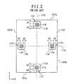
- Figs. 1 and 2 show an example of the conventional alignment marks of this sort, which is formed on a semiconductor substrate or wafer.
- the conventional alignment mark 100 shown in Figs. 1 and 2 which has been usually used for this purpose, comprises two mark elements 118 and 119.
- the inner element 119 is located in the outer element 118.
- Each of the elements 118 and 119 is square in plan shape.
- the mark 100 is formed in the following way.
- a first layer 122 is formed on the surface of a semiconductor substrate or wafer 121 and then, a patterned resist layer (not shown) is formed on the first layer 122.
- the patterned resist layer is formed by the lithography technique.
- the first layer 122 is selectively etched, thereby forming a first or lower circuit pattern (not shown) and the outer square element 118 of the alignment mark 100 in the layer 122.
- the element 118 is a square hole or opening of the layer 122.
- a second layer 123 is formed on the first layer 122 thus patterned so as to contact the bottom and side faces of the outer element 118 (i.e., the hole of the first layer 122). Then, a resist layer (not shown) is formed on the second layer 123 thus formed, and is patterned by the lithography technique, thereby forming a second or upper circuit pattern (not shown) and the inner square element 119 of the alignment mark 100 on the second layer 123 in the hole 118 of the first layer 122.
- the inner element 119 of the mark 100 is a square part of the resist layer and located in the hole or outer element 118.
- the patterned resist layer thus formed is used as a mask in the next etching process for patterning the underlying second layer 123.
- the alignment mark 110 comprising the outer and inner elements 118 and 119 thus formed is used to measure the alignment accuracy between the first circuit pattern formed by the first layer 122 and the second circuit pattern of the resist layer. In this case, the relative positional relationship between the outer and inner elements 118 and 119 is measured.
- the distance d1 between the inner side face 118a of the outer element 118 and the facing side face 119a of the inner element 119 is measured.
- the distance d2 between the opposite inner side face 118b of the outer element 118 and the facing side face 119b of the inner element 119 is measured. If the values of the distances d1 and d2 are equal, it is judged that the first or lower circuit pattern is overlaid with the second or upper circuit pattern correctly (i.e., with desired alignment accuracy) . Sometimes, it is judged whether or not the value of the difference (d1 - d2 ) between the distances d1 and d2 is within a specific range. In any of these cases, no subsequent process is applied unless it is judged that the first or lower circuit pattern is overlaid with the second or upper circuit pattern with desired alignment accuracy.
- Fig. 3 shows the layout or arrangement of the conventional alignment marks in an exposure area on a semiconductor wafer.
- four alignment marks 110, 111, 112, and 113 are provided in one of the rectangular one-shot exposure areas 107 arranged on a semiconductor wafer 10.
- Each of the marks 110, 111, 112, and 113 has the same structure as the conventional mark 100 shown in Figs. 1 and 2 .
- each of the marks 110, 111, 112, and 113 comprises the square outer and inner mark elements 118 and 119.
- the set of the four alignment marks 110, 111, 112, and 113 may be termed the "conventional alignment mark set".
- the two marks 110 and 112 are located on the longitudinal, central axis 115 of the area 107, where the direction along the axis 115 is defined as the Y direction. Since the marks 110 and 112 are on the axis 115, they are positioned at the middle of the short sides 107a and 107c of the area 107. The mark 110 is close to the upper short side 107a while the mark 112 is close to the lower short side 107c.
- the other marks 111 and 113 are located on the lateral, central axis 114 of the area 107, where the direction along the axis 114 is defined as the X direction.
- the marks 111 and 113 are on the axis 114, they are positioned at the middle of the long sides 107b and 107d of the area 107.
- the mark 111 is close to the right long side 107b while the mark 113 is close to the left long side 107d.
- a desired circuit or element pattern (not shown) is typically located among the four marks 110, 111, 112, and 113 in the area 107.
- the alignment marks 111 and 113 located on the lateral axis 114 are used. Specifically, the distances d1 and d2 between the outer and inner elements 118 and 119 along the X direction is measured for each of the marks 111 and 113. Then, the difference (d1 - d2 ) of the distances d1 and d2 is calculated. Thus, the alignment accuracy along the X direction is determined by the value of the difference (d1 - d2 ) thus calculated.
- the alignment accuracy along the Y direction is measured using the alignment marks 110 and 112 located on the longitudinal axis 115. Specifically, the distances d3 and d4 between the outer and inner elements 118 and 119 along the Y direction is measured for each of the marks 110 and 112. Then, the difference ( d3 - d4 ) of the distances d3 and d4 is calculated. Thus, the alignment accuracy along the Y direction is determined by the value of the difference ( d3 - d4 ) thus calculated.
- a lot of the rectangular exposure areas 107 shown in Fig. 3 each of which includes the conventional alignment mark set comprising the four marks 110, 111, 112, and 113, are regularly arranged on the semiconductor wafer 121, as shown in Fig. 4 .
- the exposure areas 107 are arranged in a matrix array on the wafer 121. Needless to say, the alignment accuracy is measured in each of the areas 107 using the marks 110, 111, 112, and 113.
- the conventional alignment mark set comprising the four marks 110, 111, 112, and 113
- some of the marks 110, 111, 112, and 113 are located close to each other.
- the mark 111 in one of the areas 107 and the mark 113 in another of the areas 107, which are surrounded by an ellipse 116 are close to each other.
- the mark 112 in one of the areas 107 and the mark 110 in another of the areas 107, which are surrounded by an ellipse 117 are close to each other.
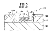
- the inner elements 119 of the marks 110, 111, 112, and 113 do not have desired contours or edges, which is explained in detail below with reference to Fig. 5 .
- the outer side face 119b tends to be tilted, as shown in Fig. 5 .
- the reason why the outer side face 119b is made oblique is not known clearly; however, it is thought in the following way.
- the exposing light irradiated to the resist layer for the inner element 119 of the mark 111 is affected by the next mark 113 to the mark 111.
- the resist layer is not exposed to the light as desired.
- the top corner of the side face 119 is broken or deformed in the development process of the resist layer.
- the contour or outline of the side face 119b is unable to be detected or observed correctly.
- the distance d2 between the side face 119b and the opposing inner face 118b of the outer element 118 tends to be measured d2' .
- the alignment accuracy thus observed tends to include some divergence or error of [( d1 - d2' )/2], which degrades the measurement accuracy.
- Document JP 9-232202 A discloses a semiconductor wafer comprising a regular matrix array arrangement of adjacent exposure areas, each of the exposure areas comprising:
- an object of the present invention is to provide an alignment mark set that facilitates the formation of a desired contour of each alignment mark, and a method of measuring alignment of patterns using the set.
- Another object of the present invention is to provide an alignment mark set that suppresses the degradation of measurement accuracy for alignment of patterns, and a method of measuring alignment of patterns using the set.
- Still another object of the present invention is to provide an alignment mark set that ensures high measurement accuracy, and a method of measuring alignment of patterns using the set.
- a semiconductor wafer according to claim 1 is provided.
- the first alignment mark is formed in the exposure area in such a way as to be located near the first axis of the area and apart from the second axis thereof.
- the second alignment mark is formed in the exposure area in such a way as to be located near the second axis of the area and apart from the first axis thereof.
- the alignment mark sets of the semiconductor wafer according to the first aspect are arranged to be adjacent to each other in a plane on use, each of the first and second alignment marks in one of the set is not located close to the first and second alignment marks in another of the sets. Accordingly, even if exposing light is irradiated to all the exposure areas thus arranged, none of the first and second alignment marks in one of the sets are affected by the first and second marks in another of the sets.
- each of the first and second marks is square.
- the first and third marks are apart from the periphery on opposite sides at equal distances while the second and fourth marks are apart from the periphery on opposite sides at equal distances. More preferably, the first and third marks are apart from the periphery at equal distances of 100 ⁇ m or greater while the second and fourth marks are apart from the periphery at equal distances of 100 ⁇ m or greater.
- a method of measuring alignment of patterns according to claim 5 is provided.
- unopposed sides of the first and third marks located on opposite sides to each other with respect to the periphery of the area and unopposed sides of the second and fourth marks located on opposite sides to each other with respect to the periphery of the area are used for measuring.
- each of the first and second marks is square.
- a lot of rectangular exposure areas 7 are regularly formed or defined on a semiconductor wafer 21; in other words, the areas 7 are arranged in a matrix array on the wafer 21.
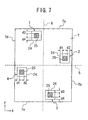
- an alignment mark set according is formed, which comprises four alignment marks 1, 2, 3, and 4, as shown in Fig. 6 .
- the four alignment marks 1, 2, 3, and 4 are arranged in such a manner as shown in Fig. 6 .
- the two marks 1 and 3 are located near the longitudinal, central axis 6 of the rectangular exposure area 7, where the direction along the axis 6 is defined as the Y direction.
- the mark 1 is near the upper short side 7a of the area 7 while the mark 3 is near the lower short side 7c thereof.
- the mark 1 is shifted (i.e., offset) from the axis 6 toward the left-hand side in Fig. 6 by a distance h1.
- the mark 3 is shifted (i.e., offset) from the axis 6 toward the right-hand side in Fig. 6 by the same distance h1.
- the distance h1 is measured from the axis 6 to the center of the mark 1 or 3.
- the remaining two marks 2 and 4 are located near the lateral, central axis 5 of the rectangular exposure area 7, where the direction along the axis 5 is defined as the X direction.
- the mark 2 is near the right long side 7b of the area 7 while the mark 4 is near the left long side 7d thereof.
- the mark 2 is shifted (i.e., offset) from the axis 5 upward in Fig. 6 by a distance h2.
- the mark 4 is shifted (i.e., offset) from the axis 5 downward in Fig. 6 by the same distance h2.
- the distance h2 is measured from the axis 5 to the center of the mark 2 or 4.
- the mark 1 comprises a square outer element 24 and a square inner element 25.
- the inner element 25 is entirely located in the outer element 24 so as to be concentric with the outer element 24.
- Each of the four sides of the inner element 25 (the length of which is L2 ) is parallel to a corresponding one of the four sides of the outer element 24 (the length of which is L1 ), where L1 > L2.
- the offset distance h1 of the mark 1 or 3 is determined in such a way as to be larger than half of the side length L1 of the mark 1 or 3, i.e., h1 > [( L1 )/2].
- the marks 1 and 3 are located apart from the longitudinal, central axis 6.
- the offset distance h2 of the mark 2 or 4 is determined in such a way as to be larger than half of the side length L1 of the mark 2 or 4, i.e., h2 > [( L1 )/2].
- the marks 2 and 4 are located apart from the lateral, central axis 5.
- Fig. 9 shows a cross-sectional view showing the structure of the mark 1, which is taken along a line like the line II-II in Fig. 1 .
- the other marks 2, 3, and 4 have the same cross-section as shown in Fig. 9 .
- the mark 1 is formed in the following way.
- a first layer 22 is formed on the surface of the semiconductor wafer 21.
- a resist layer (not shown) is formed on the first layer 22 and is patterned to have a specific shape by the lithography technique.
- the underlying first layer 22 is selectively etched, thereby forming a first or lower circuit pattern (not shown) and the outer square element 24 of the alignment mark 1 in the layer 22.
- the element 24 is a square hole formed in the layer 22.
- a second layer 23 is formed on the first layer 22 thus patterned so as to contact the bottom and side faces of the element 24 (i.e., the hole of the first layer 22).
- a resist layer (not shown) is formed on the second layer 23 and is patterned by the lithography technique, thereby forming a second or upper circuit pattern (not shown) and the inner square element 25 of the alignment mark 1 on the layer 23 in the hole 24 of the layer 22.
- the inner element 25 is a square part of the resist layer and located in the hole or outer element 24.
- the patterned resist layer thus formed is used as a mask in the next etching process for the second layer 23.
- the alignment mark set comprising the marks 1, 2, 3, and 4 of the semiconductor wafer according to the embodiment is used to measure the alignment accuracy between the first circuit pattern formed by the first layer 22 and the second circuit pattern formed by the patterned resist layer. In this case, the relative positional relationship between the inner and outer elements 25 and 24 is measured.
- the distance d1 between the inner side face 24a of the outer element 24 and the facing side face 25a of the inner element 25 is measured.
- the distance d2 between the opposite inner side face 24b of the outer element 24 and the facing side face 25b of the inner element 24 is measured. If the values of the distances d1 and d2 are equal, it is judged that the first or lower circuit pattern is overlaid with the second or upper circuit pattern correctly (i.e., with desired alignment accuracy) . Sometimes, it is judged whether or not the value difference (d1 - d2 ) between the distances d1 and d2 is within a specific range. Thus, the alignment accuracy in the X direction is obtained.
- the distance d3 between the inner side face of the outer element 24 and the facing side face of the inner element 25 is measured.
- the distance d4 between the opposite inner side face of the outer element 24 and the facing side face of the inner element 25 is measured. If the values of the distances d3 and d4 are equal, it is judged that the first or lower circuit pattern is overlaid with the second or upper circuit pattern correctly (i.e., with desired alignment accuracy). Sometimes, it is judged whether or not the value difference (d3 - d4 ) between the distances d3 and d4 is within a specific range. Thus, the alignment accuracy in the Y direction is obtained.
- the distances d1, d2, d3, and d4 are measured by the known laser-scanning method or image-processing method with a known suitable apparatus.
- the two marks 1 and 3 are respectively located in the vicinity of the short sides 7a and 7c of the rectangular exposure area 7 in such a way as to be shifted by the same distance h1 in the opposite directions with respect to the longitudinal, central axis 6.
- the remaining two marks 2 and 4 are respectively located in the vicinity of the long sides 7b and 7d of the area 7 in such a way as to be shifted by the same distance h2 in the opposite directions with respect to the lateral, central axis 5.
- Fig. 10 shows an alignment mark set according to a first example , which comprises four square alignment marks 31, 32, 33, and 34. This alignment mark set is formed in each of the rectangular exposure areas 7 arranged in a matrix array on the wafer 21, which has been referred in the first embodiment.
- the alignment marks 31, 32, 33, and 34 are formed in the following way:
- both the marks 31 and 33 are located on the longitudinal central axis 6 of the rectangular exposure area 7. In other words, these two marks 31 and 33 have no offset. Also, the mark 31 is apart from the upper short side 7a of the area 7 at a distance k1 while the mark 33 is apart from the lower short side 7c thereof at the same distance k1. The distance k1 is measured from the short side 7a or 7c to the opposing side of the mark 31 or 33. The marks 31 and 33 are apart from each other at a distance k3 along the axis 6, which is measured between the opposing sides of the marks 31 and 33 in the Y direction.
- the distance k1 is equal to or more than 50 ⁇ m. More preferably, the distance k1 is equal to or more than 100 ⁇ m.
- the distance k3 between the opposing sides of the marks 31 and 33 is set to be 100 ⁇ m or more.
- both the marks 32 and 34 are located on the lateral, central axis 5 of the rectangular exposure area 7.
- the marks 32 and 34 have no offset.
- the mark 32 is apart from the right long side 7b of the area 7 at a distance k2 while the mark 34 is apart from the left long side 7c thereof at the same distance k2.
- the distance k2 is measured from the long side 7b or 7d of the area 7 to the opposing side of the mark 32 or 34.
- the marks 32 and 34 are apart from each other at a distance k4 along the axis 5, which is measured between the opposing sides of the marks 32 and 34 in the X direction.
- the distance k2 is equal to or more than 50 ⁇ m.
- the distance k2 is equal to or more than 100 ⁇ m.
- the distance k4 between the opposing sides of the marks 32 and 34 is set to be 100 ⁇ m or more.
- the four marks 31, 32, 33, and 34 are arranged in the area 7 in such a manner as above, they are located at the shifted positions toward the center of the area 7 (i.e., the intersection of the axes 5 and 6) compared with the conventional alignment mark set comprising the marks 110, 111, 112, and 113 and the alignment mark set comprising the marks 1, 2, 3, and 4 of the embodiment.
- All the marks 31, 32, 33, and 34 are the same in shape and structure as the marks 1, 2, 3, and 4 of the first embodiment.
- the alignment mark set comprising the marks 31, 32, 33, and 34 according to the first example is used to measure the alignment accuracy between the first circuit pattern formed by the first layer 22 and the second circuit pattern. In this case, the relative positional relationship between the elements 24 and 25 is measured.
- the distances d1 between the outer and inner elements 24 and 25 of the marks 32 and 34 are measured while the distances d2 between the outer and inner elements 24 and 25 of the marks 31 and 33 are measured.
- the alignment accuracy in the Y direction is obtained.
- the distances d3 between the outer and inner elements 24 and 25 of the marks 31 and 33 are measured while the distances d4 between the inner and outer elements 24 and 25 are measured.
- the alignment accuracy in the X direction is obtained.
- the first or lower circuit pattern is overlaid with the second or upper circuit pattern correctly (i.e., with desired alignment accuracy).
- the marks 31 and 33 are respectively located on the axis 6 at the positions shifted toward the center of the exposure area 7 in such a way as to be at the same distance k1 from the short sides 7a and 7c of the area 7.
- the marks 32 and 34 are respectively located on the axis 5 at the positions shifted toward the center of the area 7 in such a way as to be at the same distance k2 from the long sides 7b and 7d thereof.
- the marks 32 and 34 surrounded by the ellipse 38 are shifted in opposite directions along the common short side of the adjoining areas 7. This means that the marks 32 and 34 are sufficiently apart from each other; in other words, none of these marks 32 and 34 apply any bad effect to each other due to the exposing light.
- Fig. 12 shows an alignment mark set used in a method of measuring alignment accuracy according to a second example .
- This set is formed in each of the rectangular exposure areas 7 arranged in a matrix array on the wafer 21, which has been referred in the embodiment.
- This set comprises four alignment marks 41, 42, 43, and 44.
- both the marks 41 and 43 are located on the longitudinal, central axis 6 of the rectangular exposure area 7.
- the marks 41 and 43 have no offset with respect to the axis 6.
- the mark 41 is close to the upper short side 7a of the area 7 at a distance while the mark 43 is close to the lower short side 7c thereof at the same distance.
- both the marks 42 and 44 are located on the lateral, central axis 5 of the area 7.
- the marks 42 and 44 have no offset with respect to the axis 5.
- the mark 42 is close to the right long side 7b of the area 7 at a distance while the mark 44 is apart from the left long side 7c thereof at the same distance.
- All the marks 41, 42, 43, and 44 are the same in shape and structure as the marks 1, 2, 3, and 4 of the first embodiment.
- the marks 41 and 43 aligned on the axis 6 are used. Specifically, the distance d1 between the inner side face of the outer element 24 of the mark 41 and the facing side face 25d of the inner element 25 thereof is measured. At the same time, the distance d2 between the opposite inner side face of the outer element 24 of the mark 41 and the facing side face 25b of the inner element 25 thereof is measured. Similarly, the distance d1 between the inner side face of the outer element 24 of the mark 43 and the facing side face 25d of the inner element 25 thereof is measured. At the same time, the distance d2 between the opposite inner side face of the outer element 24 of the mark 43 and the facing side face 25b of the inner element 25 thereof is measured.
- the marks 42 and 44 aligned on the axis 5 are used. Specifically, the distance d3 between the inner side face of the outer element 24 of the mark 42 and the facing side face 25a of the inner element 25 thereof is measured. At the same time, the distance d4 between the opposite inner side face of the outer element 24 of the mark 42 and the facing side face 25c of the inner element 25 thereof is measured. Similarly, the distance d3 between the inner side face of the outer element 24 of the mark 44 and the facing side face 25d of the inner element 25 thereof is measured. At the same time, the distance d4 between the opposite inner side face of the outer element 24 of the mark 44 and the facing side face 25b of the inner element 25 thereof is measured.
- the marks 41 and 43 are aligned in the Y direction and close to each other while the marks 42 and 44 are aligned in the X direction and close to each other.
- breaking or deformation occurs at the side face 25a of the inner element 25 of the mark 41, at the side face 25c of the inner element 25 of the mark 43, at the side face 25b of the inner element 25 of the mark 42, and at the side face 25d of the inner element 25 of the mark 44.
- the broken or deformed faces 25a and 25c of the marks 41 and 43 are not used (i.e., the faces 25b and 25d of the marks 41 and 43 are used) to measure the Y-direction accuracy.
- the broken or deformed faces 25b and 25d of the marks 42 and 44 are not used (i.e., the faces 25a and 25c of the marks 42 and 44 are used) to measure the X-direction accuracy.
- the alignment can be measured with higher accuracy than the conventional method.
- the alignment mark set is approximately the same in structure as the conventional mark set.
- any alignment mark set (including the sets according to the embodiment and first example) may be used for the method of the second example.
- the inner and outer elements 25 and 24 of every alignment mark in the exposure area 7 are square. This is to facilitate the alignment measuring operation with a measuring apparatus.
- the invention is not limited to these cases. It is needless to say that the elements 25 and 24 may have any other shape according to the necessity.
- the alignment mark set comprises four alignment marks in each exposure area. This is to facilitate the alignment measuring operation with a measuring apparatus and to simplify the pattern for the alignment mark set.
- the invention is not limited to this case. Needless to say, the set may comprise five or more alignment marks in each exposure area.
Applications Claiming Priority (2)
| Application Number | Priority Date | Filing Date | Title |
|---|---|---|---|
| JP2000042562A JP3677426B2 (ja) | 2000-02-21 | 2000-02-21 | 位置合わせ精度計測マーク |
| JP2000042562 | 2000-02-21 |
Publications (3)
| Publication Number | Publication Date |
|---|---|
| EP1128215A2 EP1128215A2 (en) | 2001-08-29 |
| EP1128215A3 EP1128215A3 (en) | 2003-07-16 |
| EP1128215B1 true EP1128215B1 (en) | 2011-04-13 |
Family
ID=18565620
Family Applications (1)
| Application Number | Title | Priority Date | Filing Date |
|---|---|---|---|
| EP01103594A Expired - Lifetime EP1128215B1 (en) | 2000-02-21 | 2001-02-21 | Semiconductor wafer with alignment mark sets and method of measuring alignment accuracy |
Country Status (6)
| Country | Link |
|---|---|
| US (1) | US6498401B2 (ja) |
| EP (1) | EP1128215B1 (ja) |
| JP (1) | JP3677426B2 (ja) |
| KR (1) | KR100381881B1 (ja) |
| DE (1) | DE60144405D1 (ja) |
| TW (1) | TW480586B (ja) |
Families Citing this family (14)
| Publication number | Priority date | Publication date | Assignee | Title |
|---|---|---|---|---|
| JP3348783B2 (ja) * | 1999-07-28 | 2002-11-20 | 日本電気株式会社 | 重ね合わせ用マーク及び半導体装置 |
| US6875624B2 (en) * | 2002-05-08 | 2005-04-05 | Taiwan Semiconductor Manufacturing Co. Ltd. | Combined E-beam and optical exposure semiconductor lithography |
| KR100546698B1 (ko) * | 2003-07-04 | 2006-01-26 | 앰코 테크놀로지 코리아 주식회사 | 반도체 패키지의 서브스트레이트 |
| JP3962713B2 (ja) * | 2003-09-30 | 2007-08-22 | キヤノン株式会社 | アライメントマークの形成方法、およびデバイスが構成される基板 |
| US7888011B2 (en) * | 2004-10-18 | 2011-02-15 | U.S. Genomics, Inc. | Methods for isolation of nucleic acids from prokaryotic spores |
| JP4610447B2 (ja) * | 2005-08-31 | 2011-01-12 | Okiセミコンダクタ株式会社 | 半導体装置とその製造方法及び検査方法 |
| CN102566255A (zh) * | 2010-12-27 | 2012-07-11 | 北大方正集团有限公司 | 一种用于曝光机对准的光罩及光罩对准标记制作方法 |
| CN102799062A (zh) * | 2012-08-29 | 2012-11-28 | 上海宏力半导体制造有限公司 | 一种掩膜版、晶圆和测机方法 |
| US8901756B2 (en) * | 2012-12-21 | 2014-12-02 | Spansion Llc | Chip positioning in multi-chip package |
| US9442391B2 (en) * | 2013-03-12 | 2016-09-13 | Taiwan Semiconductor Manufacturing Co., Ltd. | Overlay sampling methodology |
| US9595419B1 (en) * | 2013-11-27 | 2017-03-14 | Multibeam Corporation | Alignment and registration targets for multiple-column charged particle beam lithography and inspection |
| JP2016092082A (ja) * | 2014-10-30 | 2016-05-23 | キヤノン株式会社 | リソグラフィ装置、リソグラフィ方法、および物品の製造方法 |
| CN111627952B (zh) * | 2020-06-19 | 2022-04-08 | 武汉华星光电技术有限公司 | 显示面板及其制备方法、显示装置 |
| CN114171500B (zh) * | 2021-12-07 | 2024-04-09 | 成都海威华芯科技有限公司 | 一种版图定位标记绘制方法、基于其制备的芯片及晶圆 |
Citations (3)
| Publication number | Priority date | Publication date | Assignee | Title |
|---|---|---|---|---|
| JPH0228918A (ja) * | 1988-07-19 | 1990-01-31 | Fujitsu Ltd | レチクルの位置精度検出パターン形成方法 |
| US5578423A (en) * | 1993-10-15 | 1996-11-26 | Hyundai Electronics Industries Co., Ltd. | Method for the preparation of a pattern overlay accuracy-measuring mark |
| GB2316768A (en) * | 1996-08-29 | 1998-03-04 | Nec Corp | Alignment mask |
Family Cites Families (16)
| Publication number | Priority date | Publication date | Assignee | Title |
|---|---|---|---|---|
| US5262822A (en) * | 1984-11-09 | 1993-11-16 | Canon Kabushiki Kaisha | Exposure method and apparatus |
| JPH0495956A (ja) * | 1990-08-08 | 1992-03-27 | Kawasaki Steel Corp | リソグラフィマスク及びマスクパターン転写方法 |
| US5654553A (en) * | 1993-06-10 | 1997-08-05 | Nikon Corporation | Projection exposure apparatus having an alignment sensor for aligning a mask image with a substrate |
| US5446521A (en) * | 1993-06-30 | 1995-08-29 | Intel Corporation | Phase-shifted opaquing ring |
| JP3372685B2 (ja) * | 1994-12-15 | 2003-02-04 | キヤノン株式会社 | 半導体露光装置 |
| JPH08316122A (ja) * | 1995-05-18 | 1996-11-29 | Nikon Corp | 露光方法 |
| JP3624919B2 (ja) * | 1995-08-04 | 2005-03-02 | 株式会社ニコン | 露光方法 |
| JP3292022B2 (ja) * | 1996-01-17 | 2002-06-17 | キヤノン株式会社 | 位置検出装置及びそれを用いた半導体素子の製造方法 |
| JPH09232202A (ja) * | 1996-02-20 | 1997-09-05 | Mitsubishi Electric Corp | 投影露光装置におけるアライメント方法 |
| JPH09251945A (ja) * | 1996-03-15 | 1997-09-22 | Sony Corp | 重ね合わせ精度管理用パターンおよびこれを用いた重ね合わせ精度管理方法 |
| JP2904269B2 (ja) * | 1996-07-23 | 1999-06-14 | 日本電気株式会社 | アライメントマークおよびアライメント方法 |
| JPH1050589A (ja) * | 1996-08-01 | 1998-02-20 | Nikon Corp | アライメント方法 |
| JPH10284396A (ja) * | 1997-04-03 | 1998-10-23 | Nikon Corp | アライメント方法及び重ね合わせ精度計測方法 |
| JPH11162810A (ja) * | 1997-11-26 | 1999-06-18 | Mitsubishi Electric Corp | 電子ビーム露光用アラインメントマーク |
| JP4301584B2 (ja) * | 1998-01-14 | 2009-07-22 | 株式会社ルネサステクノロジ | レチクル、それを用いた露光装置、露光方法および半導体装置の製造方法 |
| KR19990070018A (ko) * | 1998-02-16 | 1999-09-06 | 구본준 | 반도체 소자의 오정렬 측정 패턴 |
-
2000
- 2000-02-21 JP JP2000042562A patent/JP3677426B2/ja not_active Expired - Fee Related
-
2001
- 2001-02-20 US US09/788,759 patent/US6498401B2/en not_active Expired - Lifetime
- 2001-02-21 DE DE60144405T patent/DE60144405D1/de not_active Expired - Lifetime
- 2001-02-21 KR KR10-2001-0008625A patent/KR100381881B1/ko not_active IP Right Cessation
- 2001-02-21 EP EP01103594A patent/EP1128215B1/en not_active Expired - Lifetime
- 2001-02-21 TW TW090103998A patent/TW480586B/zh not_active IP Right Cessation
Patent Citations (3)
| Publication number | Priority date | Publication date | Assignee | Title |
|---|---|---|---|---|
| JPH0228918A (ja) * | 1988-07-19 | 1990-01-31 | Fujitsu Ltd | レチクルの位置精度検出パターン形成方法 |
| US5578423A (en) * | 1993-10-15 | 1996-11-26 | Hyundai Electronics Industries Co., Ltd. | Method for the preparation of a pattern overlay accuracy-measuring mark |
| GB2316768A (en) * | 1996-08-29 | 1998-03-04 | Nec Corp | Alignment mask |
Also Published As
| Publication number | Publication date |
|---|---|
| KR100381881B1 (ko) | 2003-04-26 |
| TW480586B (en) | 2002-03-21 |
| JP3677426B2 (ja) | 2005-08-03 |
| EP1128215A2 (en) | 2001-08-29 |
| KR20010083217A (ko) | 2001-08-31 |
| DE60144405D1 (de) | 2011-05-26 |
| US20010021548A1 (en) | 2001-09-13 |
| EP1128215A3 (en) | 2003-07-16 |
| US6498401B2 (en) | 2002-12-24 |
| JP2001230195A (ja) | 2001-08-24 |
Similar Documents
| Publication | Publication Date | Title |
|---|---|---|
| US5733690A (en) | Reticle for fabricating semiconductor device | |
| EP0370834B1 (en) | Method of manufacturing a semiconductor device | |
| EP0061536B1 (en) | Method of manufacturing a semiconductor device having improved alignment marks and alignment marks for said method | |
| US7190823B2 (en) | Overlay vernier pattern for measuring multi-layer overlay alignment accuracy and method for measuring the same | |
| EP1128215B1 (en) | Semiconductor wafer with alignment mark sets and method of measuring alignment accuracy | |
| US6218200B1 (en) | Multi-layer registration control for photolithography processes | |
| US6645823B2 (en) | Reticle and method of fabricating semiconductor device | |
| KR100519252B1 (ko) | 오버레이 마크, 오버레이 마크 형성방법 및 오버레이측정방법 | |
| KR100315911B1 (ko) | 액정 표시 장치 패널, 그 제조 방법 및 정렬 방법 | |
| JP2669391B2 (ja) | 半導体装置 | |
| US6878506B2 (en) | Method for manufacturing semiconductor device | |
| US7136520B2 (en) | Method of checking alignment accuracy of patterns on stacked semiconductor layers | |
| JP2001092109A (ja) | フォトマスクおよび半導体装置およびフォトマスクを用いた露光方法 | |
| JP2000077312A (ja) | 半導体装置 | |
| US8031329B2 (en) | Overlay mark, and fabrication and application of the same | |
| TWI817438B (zh) | 重疊標記 | |
| JPH0831404B2 (ja) | 半導体装置の製造方法 | |
| JPH1174189A (ja) | マスクの位置ずれ検出用マーク | |
| KR960014961B1 (ko) | 반도체 장치의 제조 방법 | |
| CN116960110A (zh) | 重叠标记 | |
| KR100197981B1 (ko) | 반도체소자의 마스크 정렬 측정방법 | |
| KR20040003936A (ko) | 반도체 소자의 얼라인 마크 | |
| US20040137649A1 (en) | Method of fabricating semiconductor device comprising superposition inspection step | |
| KR20070071657A (ko) | 반도체 소자의 오버레이 버니어 형성 방법 | |
| KR20080061031A (ko) | 오버레이 마크 및 그 마크를 이용한 마스크정렬 측정방법 |
Legal Events
| Date | Code | Title | Description |
|---|---|---|---|
| PUAI | Public reference made under article 153(3) epc to a published international application that has entered the european phase |
Free format text: ORIGINAL CODE: 0009012 |
|
| AK | Designated contracting states |
Kind code of ref document: A2 Designated state(s): AT BE CH CY DE DK ES FI FR GB GR IE IT LI LU MC NL PT SE TR |
|
| AX | Request for extension of the european patent |
Free format text: AL;LT;LV;MK;RO;SI |
|
| RAP1 | Party data changed (applicant data changed or rights of an application transferred) |
Owner name: NEC ELECTRONICS CORPORATION |
|
| PUAL | Search report despatched |
Free format text: ORIGINAL CODE: 0009013 |
|
| AK | Designated contracting states |
Designated state(s): AT BE CH CY DE DK ES FI FR GB GR IE IT LI LU MC NL PT SE TR |
|
| AX | Request for extension of the european patent |
Extension state: AL LT LV MK RO SI |
|
| 17P | Request for examination filed |
Effective date: 20030606 |
|
| 17Q | First examination report despatched |
Effective date: 20031001 |
|
| AKX | Designation fees paid |
Designated state(s): DE GB |
|
| 17Q | First examination report despatched |
Effective date: 20031001 |
|
| RAP1 | Party data changed (applicant data changed or rights of an application transferred) |
Owner name: RENESAS ELECTRONICS CORPORATION |
|
| GRAP | Despatch of communication of intention to grant a patent |
Free format text: ORIGINAL CODE: EPIDOSNIGR1 |
|
| RTI1 | Title (correction) |
Free format text: SEMICONDUCTOR WAFER WITH ALIGNMENT MARK SETS AND METHOD OF MEASURING ALIGNMENT ACCURACY |
|
| GRAS | Grant fee paid |
Free format text: ORIGINAL CODE: EPIDOSNIGR3 |
|
| GRAA | (expected) grant |
Free format text: ORIGINAL CODE: 0009210 |
|
| AK | Designated contracting states |
Kind code of ref document: B1 Designated state(s): DE GB |
|
| REG | Reference to a national code |
Ref country code: GB Ref legal event code: FG4D |
|
| REF | Corresponds to: |
Ref document number: 60144405 Country of ref document: DE Date of ref document: 20110526 Kind code of ref document: P |
|
| REG | Reference to a national code |
Ref country code: DE Ref legal event code: R096 Ref document number: 60144405 Country of ref document: DE Effective date: 20110526 |
|
| PLBE | No opposition filed within time limit |
Free format text: ORIGINAL CODE: 0009261 |
|
| STAA | Information on the status of an ep patent application or granted ep patent |
Free format text: STATUS: NO OPPOSITION FILED WITHIN TIME LIMIT |
|
| 26N | No opposition filed |
Effective date: 20120116 |
|
| REG | Reference to a national code |
Ref country code: DE Ref legal event code: R097 Ref document number: 60144405 Country of ref document: DE Effective date: 20120116 |
|
| GBPC | Gb: european patent ceased through non-payment of renewal fee |
Effective date: 20120221 |
|
| PG25 | Lapsed in a contracting state [announced via postgrant information from national office to epo] |
Ref country code: GB Free format text: LAPSE BECAUSE OF NON-PAYMENT OF DUE FEES Effective date: 20120221 |
|
| PGFP | Annual fee paid to national office [announced via postgrant information from national office to epo] |
Ref country code: DE Payment date: 20160216 Year of fee payment: 16 |
|
| REG | Reference to a national code |
Ref country code: DE Ref legal event code: R119 Ref document number: 60144405 Country of ref document: DE |
|
| PG25 | Lapsed in a contracting state [announced via postgrant information from national office to epo] |
Ref country code: DE Free format text: LAPSE BECAUSE OF NON-PAYMENT OF DUE FEES Effective date: 20170901 |