EP1048483A1 - Vorrichtung mit einem halbleiterelement - Google Patents
Vorrichtung mit einem halbleiterelement Download PDFInfo
- Publication number
- EP1048483A1 EP1048483A1 EP97949194A EP97949194A EP1048483A1 EP 1048483 A1 EP1048483 A1 EP 1048483A1 EP 97949194 A EP97949194 A EP 97949194A EP 97949194 A EP97949194 A EP 97949194A EP 1048483 A1 EP1048483 A1 EP 1048483A1
- Authority
- EP
- European Patent Office
- Prior art keywords
- substrate
- chip
- card
- semiconductor chip
- semiconductor device
- Prior art date
- Legal status (The legal status is an assumption and is not a legal conclusion. Google has not performed a legal analysis and makes no representation as to the accuracy of the status listed.)
- Granted
Links
Images
Classifications
-
- G—PHYSICS
- G06—COMPUTING; CALCULATING OR COUNTING
- G06K—GRAPHICAL DATA READING; PRESENTATION OF DATA; RECORD CARRIERS; HANDLING RECORD CARRIERS
- G06K19/00—Record carriers for use with machines and with at least a part designed to carry digital markings
- G06K19/06—Record carriers for use with machines and with at least a part designed to carry digital markings characterised by the kind of the digital marking, e.g. shape, nature, code
- G06K19/067—Record carriers with conductive marks, printed circuits or semiconductor circuit elements, e.g. credit or identity cards also with resonating or responding marks without active components
- G06K19/07—Record carriers with conductive marks, printed circuits or semiconductor circuit elements, e.g. credit or identity cards also with resonating or responding marks without active components with integrated circuit chips
- G06K19/077—Constructional details, e.g. mounting of circuits in the carrier
- G06K19/0772—Physical layout of the record carrier
- G06K19/07728—Physical layout of the record carrier the record carrier comprising means for protection against impact or bending, e.g. protective shells or stress-absorbing layers around the integrated circuit
-
- G—PHYSICS
- G06—COMPUTING; CALCULATING OR COUNTING
- G06K—GRAPHICAL DATA READING; PRESENTATION OF DATA; RECORD CARRIERS; HANDLING RECORD CARRIERS
- G06K19/00—Record carriers for use with machines and with at least a part designed to carry digital markings
- G06K19/06—Record carriers for use with machines and with at least a part designed to carry digital markings characterised by the kind of the digital marking, e.g. shape, nature, code
- G06K19/067—Record carriers with conductive marks, printed circuits or semiconductor circuit elements, e.g. credit or identity cards also with resonating or responding marks without active components
- G06K19/07—Record carriers with conductive marks, printed circuits or semiconductor circuit elements, e.g. credit or identity cards also with resonating or responding marks without active components with integrated circuit chips
- G06K19/077—Constructional details, e.g. mounting of circuits in the carrier
- G06K19/07749—Constructional details, e.g. mounting of circuits in the carrier the record carrier being capable of non-contact communication, e.g. constructional details of the antenna of a non-contact smart card
-
- H—ELECTRICITY
- H01—ELECTRIC ELEMENTS
- H01L—SEMICONDUCTOR DEVICES NOT COVERED BY CLASS H10
- H01L23/00—Details of semiconductor or other solid state devices
- H01L23/48—Arrangements for conducting electric current to or from the solid state body in operation, e.g. leads, terminal arrangements ; Selection of materials therefor
- H01L23/488—Arrangements for conducting electric current to or from the solid state body in operation, e.g. leads, terminal arrangements ; Selection of materials therefor consisting of soldered or bonded constructions
- H01L23/498—Leads, i.e. metallisations or lead-frames on insulating substrates, e.g. chip carriers
- H01L23/49855—Leads, i.e. metallisations or lead-frames on insulating substrates, e.g. chip carriers for flat-cards, e.g. credit cards
-
- H—ELECTRICITY
- H01—ELECTRIC ELEMENTS
- H01L—SEMICONDUCTOR DEVICES NOT COVERED BY CLASS H10
- H01L2224/00—Indexing scheme for arrangements for connecting or disconnecting semiconductor or solid-state bodies and methods related thereto as covered by H01L24/00
- H01L2224/01—Means for bonding being attached to, or being formed on, the surface to be connected, e.g. chip-to-package, die-attach, "first-level" interconnects; Manufacturing methods related thereto
- H01L2224/10—Bump connectors; Manufacturing methods related thereto
- H01L2224/15—Structure, shape, material or disposition of the bump connectors after the connecting process
- H01L2224/16—Structure, shape, material or disposition of the bump connectors after the connecting process of an individual bump connector
-
- H—ELECTRICITY
- H01—ELECTRIC ELEMENTS
- H01L—SEMICONDUCTOR DEVICES NOT COVERED BY CLASS H10
- H01L2224/00—Indexing scheme for arrangements for connecting or disconnecting semiconductor or solid-state bodies and methods related thereto as covered by H01L24/00
- H01L2224/01—Means for bonding being attached to, or being formed on, the surface to be connected, e.g. chip-to-package, die-attach, "first-level" interconnects; Manufacturing methods related thereto
- H01L2224/42—Wire connectors; Manufacturing methods related thereto
- H01L2224/47—Structure, shape, material or disposition of the wire connectors after the connecting process
- H01L2224/48—Structure, shape, material or disposition of the wire connectors after the connecting process of an individual wire connector
- H01L2224/4805—Shape
- H01L2224/4809—Loop shape
- H01L2224/48091—Arched
-
- H—ELECTRICITY
- H01—ELECTRIC ELEMENTS
- H01L—SEMICONDUCTOR DEVICES NOT COVERED BY CLASS H10
- H01L2224/00—Indexing scheme for arrangements for connecting or disconnecting semiconductor or solid-state bodies and methods related thereto as covered by H01L24/00
- H01L2224/73—Means for bonding being of different types provided for in two or more of groups H01L2224/10, H01L2224/18, H01L2224/26, H01L2224/34, H01L2224/42, H01L2224/50, H01L2224/63, H01L2224/71
- H01L2224/732—Location after the connecting process
- H01L2224/73201—Location after the connecting process on the same surface
- H01L2224/73203—Bump and layer connectors
- H01L2224/73204—Bump and layer connectors the bump connector being embedded into the layer connector
-
- H—ELECTRICITY
- H01—ELECTRIC ELEMENTS
- H01L—SEMICONDUCTOR DEVICES NOT COVERED BY CLASS H10
- H01L24/00—Arrangements for connecting or disconnecting semiconductor or solid-state bodies; Methods or apparatus related thereto
- H01L24/01—Means for bonding being attached to, or being formed on, the surface to be connected, e.g. chip-to-package, die-attach, "first-level" interconnects; Manufacturing methods related thereto
- H01L24/42—Wire connectors; Manufacturing methods related thereto
- H01L24/47—Structure, shape, material or disposition of the wire connectors after the connecting process
- H01L24/48—Structure, shape, material or disposition of the wire connectors after the connecting process of an individual wire connector
-
- H—ELECTRICITY
- H01—ELECTRIC ELEMENTS
- H01L—SEMICONDUCTOR DEVICES NOT COVERED BY CLASS H10
- H01L2924/00—Indexing scheme for arrangements or methods for connecting or disconnecting semiconductor or solid-state bodies as covered by H01L24/00
- H01L2924/0001—Technical content checked by a classifier
- H01L2924/00013—Fully indexed content
-
- H—ELECTRICITY
- H01—ELECTRIC ELEMENTS
- H01L—SEMICONDUCTOR DEVICES NOT COVERED BY CLASS H10
- H01L2924/00—Indexing scheme for arrangements or methods for connecting or disconnecting semiconductor or solid-state bodies as covered by H01L24/00
- H01L2924/0001—Technical content checked by a classifier
- H01L2924/00014—Technical content checked by a classifier the subject-matter covered by the group, the symbol of which is combined with the symbol of this group, being disclosed without further technical details
-
- H—ELECTRICITY
- H01—ELECTRIC ELEMENTS
- H01L—SEMICONDUCTOR DEVICES NOT COVERED BY CLASS H10
- H01L2924/00—Indexing scheme for arrangements or methods for connecting or disconnecting semiconductor or solid-state bodies as covered by H01L24/00
- H01L2924/01—Chemical elements
- H01L2924/01019—Potassium [K]
-
- H—ELECTRICITY
- H01—ELECTRIC ELEMENTS
- H01L—SEMICONDUCTOR DEVICES NOT COVERED BY CLASS H10
- H01L2924/00—Indexing scheme for arrangements or methods for connecting or disconnecting semiconductor or solid-state bodies as covered by H01L24/00
- H01L2924/01—Chemical elements
- H01L2924/01078—Platinum [Pt]
-
- H—ELECTRICITY
- H01—ELECTRIC ELEMENTS
- H01L—SEMICONDUCTOR DEVICES NOT COVERED BY CLASS H10
- H01L2924/00—Indexing scheme for arrangements or methods for connecting or disconnecting semiconductor or solid-state bodies as covered by H01L24/00
- H01L2924/01—Chemical elements
- H01L2924/01079—Gold [Au]
-
- H—ELECTRICITY
- H01—ELECTRIC ELEMENTS
- H01L—SEMICONDUCTOR DEVICES NOT COVERED BY CLASS H10
- H01L2924/00—Indexing scheme for arrangements or methods for connecting or disconnecting semiconductor or solid-state bodies as covered by H01L24/00
- H01L2924/06—Polymers
- H01L2924/078—Adhesive characteristics other than chemical
- H01L2924/0781—Adhesive characteristics other than chemical being an ohmic electrical conductor
- H01L2924/07811—Extrinsic, i.e. with electrical conductive fillers
-
- H—ELECTRICITY
- H01—ELECTRIC ELEMENTS
- H01L—SEMICONDUCTOR DEVICES NOT COVERED BY CLASS H10
- H01L2924/00—Indexing scheme for arrangements or methods for connecting or disconnecting semiconductor or solid-state bodies as covered by H01L24/00
- H01L2924/10—Details of semiconductor or other solid state devices to be connected
- H01L2924/11—Device type
- H01L2924/12—Passive devices, e.g. 2 terminal devices
- H01L2924/1204—Optical Diode
- H01L2924/12042—LASER
-
- H—ELECTRICITY
- H01—ELECTRIC ELEMENTS
- H01L—SEMICONDUCTOR DEVICES NOT COVERED BY CLASS H10
- H01L2924/00—Indexing scheme for arrangements or methods for connecting or disconnecting semiconductor or solid-state bodies as covered by H01L24/00
- H01L2924/15—Details of package parts other than the semiconductor or other solid state devices to be connected
- H01L2924/161—Cap
- H01L2924/1615—Shape
- H01L2924/16195—Flat cap [not enclosing an internal cavity]
-
- H—ELECTRICITY
- H01—ELECTRIC ELEMENTS
- H01L—SEMICONDUCTOR DEVICES NOT COVERED BY CLASS H10
- H01L2924/00—Indexing scheme for arrangements or methods for connecting or disconnecting semiconductor or solid-state bodies as covered by H01L24/00
- H01L2924/15—Details of package parts other than the semiconductor or other solid state devices to be connected
- H01L2924/181—Encapsulation
-
- H—ELECTRICITY
- H01—ELECTRIC ELEMENTS
- H01L—SEMICONDUCTOR DEVICES NOT COVERED BY CLASS H10
- H01L2924/00—Indexing scheme for arrangements or methods for connecting or disconnecting semiconductor or solid-state bodies as covered by H01L24/00
- H01L2924/19—Details of hybrid assemblies other than the semiconductor or other solid state devices to be connected
- H01L2924/1901—Structure
- H01L2924/1904—Component type
- H01L2924/19041—Component type being a capacitor
-
- H—ELECTRICITY
- H01—ELECTRIC ELEMENTS
- H01L—SEMICONDUCTOR DEVICES NOT COVERED BY CLASS H10
- H01L2924/00—Indexing scheme for arrangements or methods for connecting or disconnecting semiconductor or solid-state bodies as covered by H01L24/00
- H01L2924/30—Technical effects
- H01L2924/301—Electrical effects
- H01L2924/30107—Inductance
-
- H—ELECTRICITY
- H01—ELECTRIC ELEMENTS
- H01L—SEMICONDUCTOR DEVICES NOT COVERED BY CLASS H10
- H01L2924/00—Indexing scheme for arrangements or methods for connecting or disconnecting semiconductor or solid-state bodies as covered by H01L24/00
- H01L2924/30—Technical effects
- H01L2924/301—Electrical effects
- H01L2924/3011—Impedance
-
- H—ELECTRICITY
- H01—ELECTRIC ELEMENTS
- H01L—SEMICONDUCTOR DEVICES NOT COVERED BY CLASS H10
- H01L2924/00—Indexing scheme for arrangements or methods for connecting or disconnecting semiconductor or solid-state bodies as covered by H01L24/00
- H01L2924/30—Technical effects
- H01L2924/301—Electrical effects
- H01L2924/3025—Electromagnetic shielding
-
- H—ELECTRICITY
- H01—ELECTRIC ELEMENTS
- H01L—SEMICONDUCTOR DEVICES NOT COVERED BY CLASS H10
- H01L2924/00—Indexing scheme for arrangements or methods for connecting or disconnecting semiconductor or solid-state bodies as covered by H01L24/00
- H01L2924/30—Technical effects
- H01L2924/35—Mechanical effects
- H01L2924/351—Thermal stress
- H01L2924/3511—Warping
Definitions
- the present invention relates to a thin semiconductor device, especially a highly reliable IC card having flexibility.
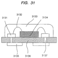
- Fig. 31 shows a sectional structure of a conventional contact-type IC card chip module. Bonding pads 3131 formed on a module substrate 3136 are connected to external terminals of a semiconductor chip 3134 through bonding wires 3132. These components are molded with a molding resin 3133. The bonding pads 3131 are connected through via holes 3137 formed in the module substrate 3136, which is a hard substrate, to contact electrodes 3135 which are for output and input of signals to and from the exterior and for the supply of electric power to an IC card.
- Fig. 34 shows a process for manufacturing an IC card which includes the IC card chip module shown in Fig. 31.
- the manufacturing process comprises an upper-side photoresist films forming step for patterning the bonding pads 3131, etc. on an upper side of the module substrate 3136, a lower-side photoresist films forming step for patterning the contact electrodes 3135, etc., a conductive film etching step using a photoresist film as a mask, a step of forming via holes 3137 in the module substrate (a glass epoxy substrate) 3136, a step of plating the interior of each via hole 3137, a step of cutting a plurality of semiconductor chips 3134 (pellets) formed separately on a semiconductor wafer, a step of bonding each of the thus-cut semiconductor chips 3134 onto the module substrate 3136, a step of bonding electrode on the semiconductor chip and the bonding pads 3131 with each other through wires 3132, a step of molding the semiconductor chip and bonding pads with resin to afford a molded chip
- Fig. 6 is a sectional view of a conventional non-contact type IC card.
- a semiconductor chip 62 and ceramic capacitors 61, 64 are mounted on a hard substrate 66. These are connected together through bonding wires and are molded with an epoxy resin 63.
- the ceramic capacitor 64 is connected to a winding coil 67 which is for output and input of signals and for the reception of energy. These components are mounted between two overcoating substrates 65 which are softer than the substrate 66.
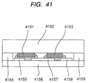
- Fig. 41 is a sectional view of an IC card in which a thin capacitor chip 4151 and a thin IC chip 4153 are mounted on a neutral surface. External terminals of the thin capacitor chip 4151 and the thin IC chip 4153 are connected, using an electrically conductive adhesive, to electrodes 4155, 4157, and 4158 which are screen-printed on a flexible substrate 4156. Further, spacers 4154 and 4159 are disposed in regions where the thin capacitor chip and the thin IC chip are not present, and an upper cover 4152 is provided opposedly to the substrate 4156 so as to cover those components.
- the IC card of the structure shown in Fig. 41 is advantageous in that the manufacturing cost is low and that the card is highly resistive to a bending stress because a thin IC chip is disposed on the neutral surface.
- the thin capacitor chip and the thin IC chip were broken easily under the action of a local compressive force (point pressure) with a ball-point pen or a pencil and that the use of the IC card is limited.
- a card-like semiconductor device having a thin, flexible IC chip 0.1 to 110 microns in thickness, wherein a reinforcing plate harder than a card substrate is provided on at least one side of the IC chip for reinforcement against a local stress. Since a local stress to be imposed on the IC chip is dispersed by the reinforcing plate, the IC chip becomes difficult to be broken.
- the reinforcing plate there may be used a metallic or resinous plate.
- the use of a metallic plate permits the formation of a thinner film than in the use of a resinous plate.
- a suitable thickness of the reinforcing plate is in the range of 1 to 110 microns. With such a degree of thickness, the reinforcing plate can be bent following a bending stress.
- the reinforcing plate may be provided on both sides of the IC chip.
- a semiconductor device of a higher reliability can be obtained by using a shade film which intercepts light (electromagnetic wave) traveling to the IC chip.
- the shade film there may be used a conductive paste.
- the shade film can be formed simultaneously with the formation of electrode or coil by printing onto a card substrate using a conductive paste.
- the reinforcing plate can be used as a shade film.
- the master and slave IC chips are connected with each other.
- the master IC chip has a function of exchanging data with the exterior, while the plural slave IC chips have a function of storing data of the same contents and issuing an "abnormal" signal upon destruction of any chip. Even in the event of destruction of any of the slave IC chips, it is possible to read out the stored data.
- Printed coil may be formed on one side or both sides of the card substrate. It may be formed on only one side in case of being used in close proximity to the IC card reader. By forming coils on both sides of the card substrate, it becomes possible to detect a weaker radio wave.
- spacers having apertures are disposed in the IC chip region and between the first and second substrates, it is possible to further improve the reliability. With such spacers, even when a stress is applied in the thickness direction of the IC card, it is possible to diminish the stress onto the IC chip. In case of a thin IC chip (50 microns or less), the spacers may be omitted.
- a semiconductor device which is an IC card
- a thin (300 microns or less) contact type IC card With a coil also provided, there is provided a multi-purpose IC card for both contact and non-contact use.
- a contact type IC card By forming a plurality of holes in a peripheral portion of an IC chip, there can be provided a contact type IC card.
- a once-write type memory as a memory provided within an IC chip, it is possible to provide an economical and safe semiconductor device. This is because the use of a once-write type memory permits reduction of the memory cell area to about half of that of E 2 PROM and further because re-write is impossible.
- a semiconductor device wherein printed electrode patterns formed on a surface of a first substrate are face-down bonded opposedly to external terminals of an IC chip, and a second substrate is disposed so as to cover the printed electrode patterns on the first substrate and also cover an upper surface of the IC chip, if a hole is formed in part of the second substrate and another substrate having electrodes on both surface and back thereof is embedded into the said hole, there can be provided a semiconductor device superior in both economy and reliability.
- an IC chip and an IC card or an IC card controlling device are electrically connected to a capacitor chip of a large capacitance, there can be provided a highly reliable IC card without loss of the storing and controlling function of the IC chip even if the supply of an electric energy to the IC chip is interrupted irregularly.
- the reinforcing plate according to the present invention there can be provided a highly reliable card-like semiconductor device which is highly resistive to a point pressure even in the use of a thin IC card having a thickness of about 100 to 250 microns.
- By printing coil patterns on both sides of a substrate it is possible to reduce the area occupied by coil.
- By using a shade film having electric conductivity it is possible to prevent a malfunction of a thin IC card caused by light, ultraviolet ray, or static electricity.
- a proximity type IC card it suffices to form a coil pattern on one side, whereby an IC card can be provided at low cost.
- an IC card By providing a thin IC chip on a neutral surface with use of a printed coil and an anisotropic conductive adhesive, it is possible to provide a less expensive, contact type IC card. Further, by forming a polyimide film on a chip surface, an IC card can be fabricated in a high yield.
- the card-like semiconductor device is employable not only as a member's card or an employee card but also as a tag to be attached to goods, electronic money, license, telephone card, railroad ticket, gift certificate, book-card, or amusement park ticket.
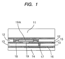
- Fig. 1 is a sectional view of a principal portion of an IC card according to the present invention.
- the numeral 11 denotes an upper cover
- numeral 12 denotes a spacer
- numeral 13 denotes a thin substrate
- numeral 14 denotes a back cover
- numeral 15 denotes a surface-side coil
- numeral 16 denotes a back-side coil
- numeral 17 denotes a through hole
- numeral 18 denotes a thin substrate electrode
- numeral 19 denotes a conductive adhesive
- numeral 19A denotes an IC chip.
- the IC chip 19A is about 50 ⁇ m thick and is flexible.
- the coils 15 and 16 are formed on both sides of the thin substrate 13 (about 50 ⁇ m thick) by printing, using a conductive paste. Both coils are connected together through the through hole 17.
- the IC chip 19A is connected to the coil 15 and the electrode 18 using the conductive adhesive 19.
- the IC chip 19A is laminated to both upper cover 11 and back cover 14 in a sandwiched fashion and the spacers 12 are placed around the IC chip to ensure the surface flatness.
- An antenna of a non-contact IC card is formed by both surface-side and back-side coils. Since the IC chip 19A is disposed on a neutral surface, the upper cover 11 is formed thicker than the back cover 14. In this embodiment the total thickness of the thin substrate 13, back cover 14 and coils 15, 16 is set approximately equal to the thickness of the upper cover.
- the chip used may range in thickness from 0.1 to 110 microns.
- the thickness of the IC card can be adjusted by selecting a suitable thickness of the upper cover and that of the back cover. It is desirable that the IC chip 19A be disposed on a neutral surface of the IC card, but in practical use a 30% error of the IC card thickness from a neutral surface of the card is allowed.
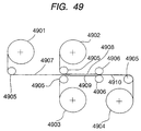
- numeral 4901 denotes a roll on which is wound a thin substrate sheet with IC chips mounted thereon
- numeral 4907 denotes the thin substrate sheet with IC chips mounted thereon
- numeral 4902 denotes a roll with an upper cover sheet wound thereon
- numeral 4908 denotes the upper cover sheet
- numeral 4903 denotes a roll with a lower cover sheet wound thereon
- numeral 4909 denotes the lower cover sheet
- numeral 4910 denotes an IC card sheet which comprises the substrate sheet with IC chips mounted thereon and the upper and lower cover sheets bonded thereto
- numeral 4904 denotes a roll with the IC card sheet wound thereon
- numeral 4905 denotes a guide roller
- numeral 4906 denotes a pressure roller for laminating the upper and lower sheets to the substrate sheet.
- the upper cover sheet 4908 and the lower cover sheet 4909 are laminated to the substrate sheet 4907 in a sandwiching fashion.
- the IC card sheet thus obtained as a laminate is then cut into a predetermined size, whereby IC cards can be obtained.
- the adhesive may be applied to the upper and lower cover sheets.
- Fig. 2 is a plan view of an IC card according to the present invention.
- a printed coil 23 and an IC chip 22 are mounted on a card substrate 21.
- MPU microprocessor unit
- TR high-frequency circuit
- FC flexible condenser
- An emboss area shown in the same figure indicates an area in which, for example, an ID number of a person who holds the IC card is displayed. It is effective for the reinforcing plate to be disposed in the area where the MPU is present. If the reinforcing plate is disposed so as to also cover the area where the TR and FC are present, it is possible to improve the reliability of the IC card.
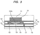
- Fig. 3 is a sectional view of a principal portion of a card-like semiconductor device provided with a reinforcing plate.
- the same reference numerals as in Fig. 1 represent the same portions as in Fig. 1.
- An upper surface of an IC chip 19A is backed with a reinforcing plate 31 which is higher in Young's modulus than the base material of the card. It is preferable that the size of the reinforcing plate 31 be larger than that of the IC chip, but in practical use the size of the reinforcing plate 31 may be equal to or somewhat (several %) smaller than that of the IC chip.
- the thickness of the reinforcing plate 31 may be set in the range of 10 to 1,000 percent of the thickness of the IC chip 19A. Preferably, the thickness of the reinforcing plate 31 is several ten microns.
- Fig. 4 is a sectional view showing how to mount a reinforcing plate to a cover substrate.
- a reinforcing plate 42 e.g., a stainless steel plate
- a cover substrate 41 e.g., a PET substrate
- a spacer 43 having about the same thickness as the thickness of the reinforcing plate 42 is affixed to the cover substrate 41 around the reinforcing plate.
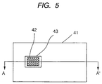
- Fig. 5 is a plan view of the cover substrate having the reinforcing plate and Fig. 4(c) is a sectional view taken on line A-A' in Fig. 5.
- An IC chip is disposed in a plane area where the reinforcing plate is provided.
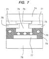
- Fig. 7 is a sectional view of a principal portion, showing a connection between an external terminal of an IC chip and an electrode of a thin substrate in a card-like semiconductor device according to the present invention.
- An insulating film 71 and a polyimide film 75 are formed around an electrode 73 which is present on a main surface of an IC chip 74.
- a gold film 72 (an external terminal of the IC chip) is formed by plating on the surface of the electrode 73.
- the gold film 72 is connected to an electrode 77 formed on a thin substrate 78.
- the gold film 72 and the electrode 77 are electrically connected with each other through fine conductive particles 76 of 1 to 20 microns contained in the anisotropic conductive adhesive.
- a projecting height of the gold film 72 from the polyimide film 75 be larger than the diameter of the conductive particles 76.
- the Young's modulus of the polyimide film 75 be lower than that of the insulating film 71, whereby it is possible to prevent a local stress from being attacked against the IC chip 74 by the conductive particles 76.
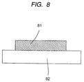
- a semiconductor chip 81 whose back side has concaves and convexes of 0.1 to 3 microns may be mounted on a card substrate 82.
- Such concaves and convexes are formed when the back of a wafer with plural semiconductor chips formed thereon is made into a thin film by spin etching.
- the IC chip which has been made into a thin film by spin etching is strong against bending and load.
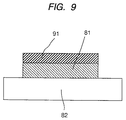
- a damage layer 91 resulting from a mechanical grinding performed to thin the semiconductor substrate.
- the said damage layer causes cracks, with the result that the IC card becomes low in mechanical strength.
- the damage layer is removed by a chemical treatment.
- chemicals there may be used fluoronitric acid, potassium hydroxide, ammonia water, and hydrazine.
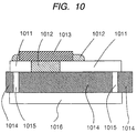
- Fig. 10 is a sectional view of a principal portion, showing a case where a plane layout area of the back coil (back pattern) shown in Fig. 1 was extended to a plane layout area of an IC chip.
- An external terminal of a thin IC chip 1013 is connected to a surface electrode pattern 1011 with a conductive adhesive 1012.
- the surface electrode pattern 1011 is formed on a flexible substrate 1014 by screen printing for example and is connected to a back pattern 1016 via through holes 1015. It is preferable that the size of the back pattern 1016 be equal to or larger than the size of the chip 1013.
- the back pattern is employable as a shade film by using a light shielding material.
- the surface pattern 1011 and the back pattern 1016 may be combined together to form printed coils.
- the back pattern can be used as a reinforcing plate against a point pressure.
- the IC chip With a sheet bonded or laminated to an upper or lower surface of the thin IC chip 1013, the IC chip is disposed on a neutral surface of an IC card.
- the neutral surface as referred to herein tolerates a displacement of 30% of the card substrate thickness from an ideal neutral surface position in the accuracy of the manufacturing process.
- Fig. 11 shows a plane structure of an IC card according to the present invention.
- this IC card is of a configuration having three thin film chips mounted thereon, no limitation is made thereto. It is optional whether the number of chip is to be one or a plural number. Further, IC chips may be laminated together.
- a thin microprocessor chip 1121, a thin transceiver chip 1127, and a thin capacitor chip 1126 are mounted on an IC card substrate 1122. These components may be constituted by a single chip.
- Surface patterns 1124 are connected to back patterns 1125 via through holes 1123. Thus, efficient coil patterns of a small area are formed.
- the coil shape various shapes of patterns are formed according to system design conditions, provided a common point is to form both surface and back patterns. Where required, part of the back pattern is placed right under the back of an IC chip to protect the IC chip electrically, mechanically and chemically from ultraviolet ray, static electricity, electromagnetic wave, chemicals, and sunlight.
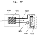
- Fig. 12 is a plan view of a principal portion of a card-like semiconductor device according to the present invention.
- a back protective pattern 1231 is formed on the lower surface side of an IC chip 1232 so as to be opposed to a main surface of the IC chip.
- An upper-side pattern 1233 of coil is connected to a back pattern 1235 through a through hole 1236 and is again exposed as a pattern to the upper side through a through hole 1234.
- the back protective pattern 1231 and the back pattern 1235 can be formed in a single process.
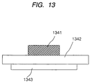
- Fig. 13 is a sectional view of a principal portion where the back protective pattern in the semiconductor device shown in Fig. 12 is formed.
- a back protective pattern 1343 is formed on the underside of a substrate 1342 and the size thereof is larger than that of an IC chip 1341.
- the back protective pattern 1343 is employable as a shade film or as a protective sheet against a point pressure.
- Fig. 14 shows a manufacturing process for a card-like semiconductor device according to the present invention.
- a flexible substrate 1451 a PET substrate 50 ⁇ m thick
- a conductive paste to form a conductive pattern 1452 having a thickness of about 20 ⁇ m.
- the conductive pattern 1452 may be formed separately as a back coil portion and a back protective layer portion.
- through holes 1453 for connection between the back coil portion and a surface coil are formed with a punch.
- a conductive pattern 1454 including the surface coil is printed on the surface of the substrate 1451 with use of silver paste.
- the silver paste is buried into the through holes 1453 by thixotropy to afford connecting plugs 1455 (Fig. 14(c)).
- a thin IC chip 1456 is bonded onto the upper surface of the substrate with upper and lower patterns formed thereon (Fig. 14(d)).
- a card-like semiconductor device (Fig. 15).
- the spacer 1561 is for diminishing the difference in height among a thin IC chip 1564, conductive adhesive 1565, and conductive paste 1562.
- conductive patterns 1567 which include a back coil portion and a back protective layer portion, using a conductive paste.
- Numeral 1569 denotes a through hole.
- Fig. 16 is a sectional view of a principal portion of such a semiconductor device.
- a surface pattern 1672 and a back pattern 1674 which are formed on the surface and the back, respectively, of a first substrate 1671, are connected together via through holes 1673.
- a second substrate 1676, a third substrate 1677, and a fourth substrate 1678 are also formed with patterns on the respective surfaces and backs. These substrates are connected together in a stacked state, for example in such a manner that the first and second substrates are connected with each other using a conductive adhesive 1675.
- On the third substrate is mounted a thin IC chip 1679.
- a proximity type IC card does not require a coil having large inductance.
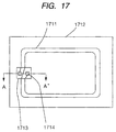
- a coil 1711 constituted by a single line may be provided on only one surface side of a substrate 1712 of the IC card. This coil is connected to electrodes 1714 of a thin IC chip 1713.
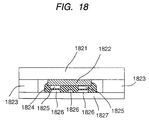
- Fig. 18 is a sectional view taken on line A-A' in Fig. 17.
- the numeral 1822 denotes a thin, flexible IC chip of 0.1 to 110 microns
- numeral 1827 denotes a thin substrate
- numeral 1824 denotes an anisotropic conductive adhesive
- numeral 1826 denotes a substrate-side electrode
- numeral 1825 denotes an IC chip-side electrode (external terminal)
- numeral 1823 denotes a spacer
- numeral 1821 denotes a cover.
- the IC chip 1822 is disposed on a neutral surface. Although a lower cover is not provided in this figure, there may be used a lower cover for making the IC card thickness into a predetermined thickness.
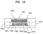
- Fig. 19 shows an example in which, in the IC card of Fig. 18, a reinforcing plate 1931 is disposed in close contact with the back of the IC chip.
- the numeral 1922 denotes a thin, flexible IC chip of 0.1 to 110 microns
- numeral 1927 denotes a thin substrate
- numeral 1924 denotes an anisotropic conductive adhesive
- numeral 1926 denotes a substrate-side electrode
- numeral 1925 denotes a IC chip-side electrode (an external terminal)
- numeral 1923 denotes a spacer
- numeral 1921 denotes a cover.
- the IC chip 1922 is disposed on a neutral surface.
- a reinforcing layer 1931 formed of a material higher in Young's modulus than the cover 1921 is buried into the same cover. With this reinforcing layer, cracking of the thin chip caused by a point pressure or a concentrated load is suppressed, whereby it is possible to improve the reliability.
- a lower cover is not provided in this figure, there may be used a lower cover to adjust the IC card thickness into a predetermined thickness.
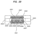
- Fig. 20 shows a structure in which an IC chip is sandwiched between reinforcing layers 2031 and 2041.
- the numeral 2022 denotes a thin, flexible IC chip of 0.1 to 110 microns
- numeral 2027 denotes a thin substrate
- numeral 2024 denotes an anisotropic conductive adhesive
- numeral 2026 denotes a substrate-side electrode
- numeral 2025 denotes an IC chip-side electrode (an external terminal)
- numeral 2023 denotes a spacer
- numeral 2021 denotes a cover.
- the IC chip 2022 is disposed on a neutral surface. This configuration permits the mechanical strength to be further enhanced.
- Buried in the cover 2021 is a reinforcing layer 2031 which is formed of a material higher in Young's modulus than the cover. According to this structure it is possible to provide a non-contact IC card of a low cost in which the thin chip is difficult to be cracked by a point pressure or a concentrated load. Further, there is attained a sufficiently high mechanical strength because of a buried reinforcing layer 2041 which is formed of a material higher in Young's modulus than the thin substrate 2027.
- reinforcing layers can be provided on both upper and lower sides of an IC chip.
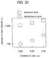
- Fig. 21 shows data on the strength of a point pressure measured with tungsten placed near a thin IC chip, tungsten having a high Young's modulus. From the same figure it is seen that the mechanical strength against a point pressure is improved.
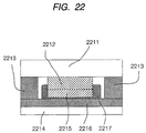
- Fig. 22 shows an example in which a reinforcing plate having about the same size as an IC chip is used.
- a thin IC chip 2215 is backed with a reinforcing plate 2212 of about the same size (within several %) as the IC chip, the reinforcing plate 2212 being formed of a material higher in Young's modulus than a cover sheet 2211.
- a conductive adhesive 2217 an external terminal of the IC chip 2215 is connected to an electrode formed on a thin substrate 2216, which external terminal and electrode are not shown.
- the IC chip 2215 and the reinforcing plate 2212, together with a spacer 2213 disposed around them, are laminated in a sandwiched fashion to both a lower sheet 2214 and a cover sheet 2211. In this way there can be obtained an IC card having a high compressive strength.
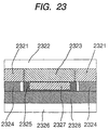
- Fig. 23 shows an example in which separate spacers 2321 and 2324 are disposed for a reinforcing plate 2323 and an IC chip 2327, respectively.
- the structure illustrated in the same figure permits easy planarization of an IC card.
- the numeral 2322 denotes an upper cover sheet
- numeral 2325 denotes an anisotropic conductive adhesive
- numeral 2326 denotes a lower cover
- numeral 2328 denotes a thin substrate.
- the upper cover sheet 2322 has a larger size than the IC chip 2327 which is thin, and is disposed so as to cover the IC chip.
- the IC chip is laminated together with the substrate 2328, lower cover 2326, and spacer 2324 to afford a thin IC card highly resistive to a point pressure and having a flat surface and a thickness of 100 to 760 microns.
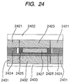
- Fig. 24 shows an example in which an IC chip 2427 is sandwiched in between two reinforcing plates 2423 and 2432 and spacers 2421, 2431, and 2424 are disposed for the reinforcing plates and the IC chip.
- the numeral 2422 denotes one cover sheet
- numeral 2433 denotes the other cover sheet
- numeral 2425 denotes an anisotropic conductive adhesive
- numeral 2428 denotes a thin substrate.
- the reinforcing plates 2423 and 2432 are formed of a material higher in Young's modulus than the cover sheets 2433 and 2422 and can withstand a bad environment against a mechanical stress.
- the thin IC chip itself is stably bonded to the thin substrate 2428 with the conductive adhesive 2425.
- the surface of the resulting IC card is planarized by the spacers 2421, 2424, and 2431. Even when a bending stress is applied to the IC card, it is possible to diminish the stress imposed on the IC chip. Since spacers are used for each of the reinforcing plates and the IC chip, the constituent layers may be formed separately and then laminated together, which is suitable for mass production.
- the spacers can be omitted by adjusting the thickness of the adhesive.
- Fig. 25 shows an example in which a reinforcing plate 2542 and a spacer 2541 are added to the structure shown in Fig. 22.
- the numeral 2511 denotes one cover sheet
- numeral 2543 denotes the other cover sheet
- numeral 2512 denotes an IC chip
- numeral 2523 denotes a reinforcing plate attached to the back of the IC chip
- numeral 2513 denotes a spacer
- numeral 2516 denotes a thin substrate
- numeral 2517 denotes an anisotropic conductive adhesive.
- the reinforcing plate 2542 is formed of a material higher in Young's modulus than an upper sheet 2511 and a lower sheet 2543.
- the surface of the IC card is planarized by the spacers 2541 and 2513.
- the thin IC chip 2512 is backed with the reinforcing plate 2523 formed of a material having a high Young's modulus and is mounted on the substrate 2516 which is flexible and thinner than the thin IC chip 2512. This structure permits a stable production of a highly reliable IC card which is strong against a point pressure.
- Fig. 26 shows an example of a plane structure of the IC cards illustrated in Figs. 22 to 25.
- a microprocessor chip 2651, a transceiver chip 2654, and a capacitor chip 2655, which have been made as thin as 50 ⁇ m or so, are mounted on an IC card substrate 2652. These are electrically connected with one another.
- the transceiver chip 2654 is connected to a conductive pattern 2657 (including a coil portion) which is formed on the surface side of a thin substrate by screen printing.
- the conductive pattern 2657 is connected through a through hole 2653 to a conductive pattern 2656 which is formed on the back side of the thin substrate.
- the back-side conductive pattern is illustrated using a straight line, it may be formed in a coil shape, whereby it is possible to handle a feebler signal and also possible to extend the distance of a remote operation.
- Figs. 27(a) to (c) are sectional views showing a process of mounting (backing by metal) reinforcing plates to a cover sheet
- Fig. 27(d) is a plan view of the sheet after the mounting of the reinforcing plates.
- the numeral 2761 denotes a cover sheet, for which PET is employable
- numeral 2762 denotes a reinforcing plate, for which tungsten or stainless steel are employable
- numeral 2763 denotes a sheet-like spacer.
- a thin sheet 2761 is provided (Fig. 27(a)).
- reinforcing plates (several millimeters square) are attached to the thin sheet (Fig. 27(b)).
- the thickness of each reinforcing plate is in the range from 1 to 110 microns and is preferably about the same as the thickness of a thin IC chip.
- a spacer sheet 2763 having apertures formed correspondingly to the positions of the reinforcing plates is affixed to the thin sheet 2761.
- Fig. 27(d) is a plan view of the sheet shown in Fig. 27(c). In this way a cover sheet with reinforcing plates can be fabricated easily.
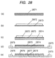
- Figs. 28(a) to (e) illustrate how to fabricate an IC chip provided with the reinforcing plate 2212 shown in Fig. 22.
- a wafer 2871 having a large number of IC chips formed thereon is provided (Fig. 28(a)).
- a support sheet 2872 is affixed to the main surface side of the wafer and the back of the wafer is removed by a spin etching system to make a wafer 2873 as thin as 1 to 110 microns (Fig. 28(b)).
- a metal plate 2874 of about the same size as the wafer is affixed to the back of the thinned wafer (Fig. 28(c)).
- the wafer with the metal plate is affixed to a dicing tape having frames 2875 and the support sheet is removed (Fig. 28(d)).
- dicing grooves 2876 As shown in Fig. 28(e), there is completed a thin chip 2877 having a thin backing metal 2878. In this way thin metal-backed chips can be mass-produced efficiently.
- the numeral 5001 denotes a conductive pattern
- numeral 5002 denotes a card substrate
- numeral 5003 denotes a thin chip
- numeral 5004 denotes a reinforcing plate
- numeral 5005 denotes a cover sheet
- numeral 5006 denotes an adhesive.
- conductive patterns 5001 are formed on a card substrate 5002 (Fig. 50(a)).
- external terminals formed on one side of a thin chip and conductive patterns are connected together using an anisotropic conductive adhesive (not shown) (Fig. 50(b)).
- a reinforcing plate 5004 is mounted on the opposite side of the thin chip (Fig. 50(c)).
- the thin chip and the reinforcing plate are fixed together using a bubble separation film.
- a cover sheet 5005 is bonded to the card substrate 5002 using an adhesive 5006 (Fig. 50(d)). According to this method there can be attained the simplification of structure and the reduction of manufacturing cost.
- the cover sheet is provided on only one side of the card substrate, it may also be provided on the opposite side of the card substrate where required (for example, for disposing the thin chip on a neutral surface of a card-like semiconductor device or for protecting one of conductive patterns if formed on both sides of the card substrate).
- the semiconductor device of the illustrated structure can be mass-produced by the method shown in Fig. 49, using the substrate sheet with the thin chip and the reinforcing plate mounted thereon, as well as the cover sheet, or using the substrate sheet with the thin chip mounted thereon and the cover sheet with the reinforcing plate mounted thereon.
- Fig. 29 shows a semiconductor device wherein a conductive pattern 2914 formed on a thin substrate 2915 is exposed.
- the numeral 2912 denotes an upper cover sheet
- numeral 2911 denotes an aperture formed in the upper cover sheet
- numeral 2913 denotes an adhesive
- numeral 2916 denotes a semiconductor chip.
- the upper cover sheet 2912 has an aperture 2911 to which the conductive pattern is exposed, and is bonded to the underlying thin substrate 2915 with an adhesive 2913.
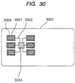
- Fig. 30 is a plan view showing an example of a semiconductor device having the structure illustrated in Fig. 29 in which the conductive pattern is exposed.
- the numeral 3021 denotes an aperture formed in a cover sheet
- numeral 3025 denotes a conductive pattern area exposed to the aperture
- numeral 3024 denotes a semiconductor chip
- numeral 3022 denotes a conductive pattern which constitutes a wiring for connection between the conductive pattern area 3025 and a semiconductor chip 3024
- numeral 3023 denotes an IC card.
- Apertures 3021 are formed in the cover sheet so that exposed conductive pattern areas 3025 can contact the opening portions respectively from the exterior.
- Wiring patterns 3022 are connected to the semiconductor chip 3024 through electrodes. This structure can afford a contact type IC card.
- Fig. 32 shows an example of a connection structure between external terminals of a semiconductor chip and electrode portions of conductive patterns formed on a thin substrate.
- Each pad 3242 (external terminal) formed on the surface of a semiconductor chip 3241 is connected to a substrate pattern 3245 formed on the surface of a thin substrate 3246, using an adhesive 3244 (an anisotropic conductive adhesive) which contains conductive particles 3243.
- the semiconductor chip 3241 is covered with a cover sheet 3247.
- the conductive particles are formed using gold and have a size of 5 to 10 microns. The use of an anisotropic conductive adhesive makes wire bonding unnecessary and permits reduction in thickness and in the number of manufacturing steps.
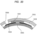
- Fig. 33 is a sectional view of a principal portion of the semiconductor device shown in Fig. 29 which is in a bent state.
- the numeral 3351 denotes a semiconductor chip
- numeral 3352 denotes a cover sheet
- numeral 3353 denotes an adhesive
- numeral 3354 denotes a conductive pattern
- numeral 3355 denotes a thin substrate
- numeral 3356 denotes an aperture.
- the semiconductor chip 3351 is connected to the conductive pattern 3354 and is covered with the cover sheet 3352 having the aperture 3356.
- the thickness of the semiconductor device is set at 300 microns or less it is possible to provide a contact type IC card capable of being bent.
- the card substrate is provided with a magnetic tape, it is possible to provide an IC card which also serves as the conventional magnetic card. Moreover, by constituting this semiconductor chip as a once-write type memory, the memory size become about half of E2PROM and it is easy to ensure security.
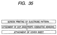
- Fig. 35 is a flow chart showing an IC card fabricating method according to the present invention.
- the formation of upper- and lower-side photoresist patterns in the flow of Fig. 34 can be done by electrode pattern screen printing.
- the conventional two steps of pellet bonding and wire bonding can be substituted by a single step of chip bonding which uses an anisotropic conductive film.
- the conventional steps of transfer molding, card substrate milling, adhesive spreading, and attachment of molded chip can be done in a cover sheet attachment step involving sandwiching an IC chip, the manufacturing process is simplified and it is possible to fabricate an IC card at a low cost.
- Fig. 36 shows an example in which the structure of an aperture in the semiconductor device shown in Fig. 29 is improved. More specifically, a substrate comprising a contact electrode 3681 and an electrode 3683 connected together through a through conductor 3682 is buried in an aperture 3611 and is connected to a conductive pattern 3614 using an anisotropic conductive adhesive for example. According to this structure it is possible to improve the flatness of the contact portion and contact reliability.
- the numeral 3612 denotes a cover sheet
- numeral 3613 denotes an adhesive
- numeral 3615 denotes a thin substrate
- numeral 3616 denotes a semiconductor chip.
- Fig. 37 is a plan view of a semiconductor device provided with a first thin chip 3711 and a second thin chip 3714 both for storing the same information.
- numeral 3712 denotes an IC card
- numeral 3713 denotes a conductive pattern including a coil. Since the same information is stored plural places, it is possible to enhance the possibility of data recovery even in the event of destruction of the IC card.
- a conventional IC card is shown in Fig. 38.
- the numeral 3821 denotes an IC chip containing memory
- numeral 3822 denotes an IC card
- numeral 3823 denotes a coil.
- this structure there is used only one chip, so in the event of destruction by cracking for example, recovery is very difficult and a large amount of money or a large volume of important data such as secret key are lost, with consequent strong likelihood of the social credit being lost.
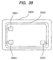
- Fig. 39 shows a semiconductor device provided with a first thin chip 3931, a second thin chip 3934, and a third thin chip 3935, each having memory capable of storing the same contents.
- the numeral 3932 denotes a card-like semiconductor device and numeral 3933 denotes a conductive pattern. Since it is rarely the case that three chips are destroyed at a time, there can be ensured a higher reliability than in the semiconductor device shown in Fig. 37.
- Fig. 40 shows a modification of the semiconductor device illustrated in Fig. 37.
- the numeral 4042 denotes a first thin chip
- numerals 4041 and 4044 denote external electrodes of the first thin chip
- numeral 4045 denotes an IC card
- numeral 4046 denotes a conductive pattern
- numeral 4048 denotes a second thin chip
- numerals 4047 and 4049 denote external electrodes of the second thin chip.
- a conductive pattern 4046 including a coil printed on one side only of a thin substrate (not shown).
- a loop having one end connected to a first electrode 4041 of the first thin chip 4042 and an opposite end connected to a second electrode 4044 of the first thin chip and a loop having one end connected to a first electrode 4047 of the second thin chip 4048 and an opposite end connected to a second electrode 4049 of the second thin chip. Since one-side printing will do for both loops, it is possible to improve the economy.
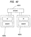
- Fig. 42 illustrates the architecture of thin chips and antenna (coils) used in the semiconductor device shown in Fig. 37.
- Two thin chips 4262 and 4263 are connected to an antenna 4261.
- the thin chips are each provided with an RF (radio frequency) circuit (a high-frequency circuit) and memory.
- the same contents are stored in the memories, so in the event of destruction of one memory, there will occur an impedance variation in the antenna. This impedance variation may be used to detect an alarm. Consequently, it is possible to detect destruction of the semiconductor chip and let information be re-stored in another memory means (another IC card).
- Fig. 43 is a modification of the architecture shown in Fig. 42.
- An RF circuit chip 4372 is connected to an antenna 4371.
- this RF circuit as a master, there are included two slave memories 4373 and 4374. Even in the event of destruction of any one chip, it is possible to read the memory contents. Further, by utilizing the point that the status in destruction is different, it is possible to derive an alarm signal from the antenna.
- the RF circuit is made separate and independent, it is possible to select suitable memories out of various memories, thus permitting fabrication of IC cards according to applications.
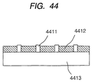
- Fig. 44 is a sectional view showing external terminal portions of a thin chip 4413.
- the numeral 4411 denotes a gold-plated bump and numeral 4412 denotes a polyimide resin.
- the gold-plated bumps 4411 are formed on the surface of the thin chip 4413, with polyimide resin 4412 being filled in between adjacent bumps.
- the presence of the polyimide resin on the surface of the thin chip is advantageous in that it is possible to diminish the occurrence of flaws on the thin chip surface caused by particles at the time of bonding the chip to a card substrate using an anisotropic conductive film.
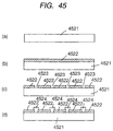
- Figs. 45(a) to (d) illustrate a conventional external terminal manufacturing process which can be applied for obtaining the above structure.
- a polyimide film as an example.
- a semiconductor wafer 4521 with a semiconductor device formed on the surface thereof is provided (Fig. 45(a)).
- the wafer surface is coated with a polyimide film 4522 (Fig. 45(b)).
- the polyimide film thus coated on the wafer surface is then subjected to a photoresist step to form apertures 4523 for electrode portions (Fig. 45(c)).
- gold-plated portions 4524 are formed in the apertures, as shown in Fig. 45(d).
- the conventional process requires the photoresist step, which is uneconomical.
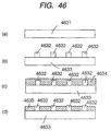
- a wafer 4631 with a semiconductor device already formed thereon is provided (Fig. 46(a)).
- gold-plated bumps 4632 are formed on a surface-treated wafer 4633 (Fig. 46(b)).
- the wafer 4633 is coated with a polyimide resin film 4634 throughout the whole surface thereof (Fig. 46(c)).
- the surface of the polyimide resin film is subjected to an ashing treatment to expose the surfaces of the gold-plated bumps, allowing the polyimide resin film 4635 present in the gold bump-free area to remain (Fig. 46(d)).
- the photoresist step for the polyimide film is not needed, permitting a low-cost production.
- plastic seal there has been used a polyimide film for reducing a stress applied to wiring on the surface of an IC chip and for preventing migration thereby. Therefore, the use of a polyimide film has not always been necessary.
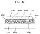
- Fig. 47 is a sectional view showing a connection between conductive patterns 4745 formed on a thin substrate 4746 and external terminals 4742 of a thin chip 4743.
- the numeral 4744 denotes a polyimide resin film
- numeral 4741 denotes an anisotropic conductive adhesive
- numeral 4747 denotes conductive particles contained in the anisotropic conductive adhesive.
- the conductive pattern electrodes 4745 formed on the thin substrate 4746 fine conductive particles are pressed down strongly to a buried extent for securing the connection. Since the polyimide resin film 4744 is formed between gold-plated bumps (external terminals) 4742, there can be ensured a stable connection without damaging the surface of the thin chip 4743 even when attacked by hard conductive particles 4747 contained in the anisotropic conductive adhesive 4741.
- Fig. 48 is a plan view showing a layout example of gold-plated bumps 4852 on a wafer 4851. Generally, bumps are formed in a peripheral area of a semiconductor chip.
- a card-like semiconductor device illustrated in this figure by sending and receiving signals to and from a card reader, is applicable as electronic money, member's card, credit, electronic key, resident card, health insurance card, license, commutation ticket, electronic ticket, or electronic slip.
- an employee card having memory in which are stored the name of the company, assigned post, name of the person, and employee number.
- this employee card is read by a card reader disposed on a reception desk of each work section and is collated with information stored separately (in a computer for management), whereby it is possible to check whether the person carrying the employee card is the very person.
- a ticket acquired in exchange for a charge is read by a card reader disposed in an entrance gate and, on the basis of the read information, a check is made to see if the ticket is proper or not, then if the ticket is proper, the gate is opened to permit entrance.
- a card-like semiconductor device provided with a reinforcing plate is strong against not only a bending stress but also a local stress, so is employable even under a mechanically severe environment.
- the present invention is applicable to electronic money, member's card, credit, electronic key, resident card, health insurance card, license, commutation ticket, electronic ticket, or electronic slip.
Landscapes
- Engineering & Computer Science (AREA)
- Computer Hardware Design (AREA)
- Microelectronics & Electronic Packaging (AREA)
- Physics & Mathematics (AREA)
- General Physics & Mathematics (AREA)
- Theoretical Computer Science (AREA)
- Condensed Matter Physics & Semiconductors (AREA)
- Power Engineering (AREA)
- Credit Cards Or The Like (AREA)
Applications Claiming Priority (1)
| Application Number | Priority Date | Filing Date | Title |
|---|---|---|---|
| PCT/JP1997/004738 WO1999032304A1 (en) | 1997-12-22 | 1997-12-22 | Semiconductor device |
Publications (3)
| Publication Number | Publication Date |
|---|---|
| EP1048483A1 true EP1048483A1 (de) | 2000-11-02 |
| EP1048483A4 EP1048483A4 (de) | 2002-08-07 |
| EP1048483B1 EP1048483B1 (de) | 2007-07-11 |
Family
ID=14181708
Family Applications (1)
| Application Number | Title | Priority Date | Filing Date |
|---|---|---|---|
| EP97949194A Expired - Lifetime EP1048483B1 (de) | 1997-12-22 | 1997-12-22 | Kartenförmige vorrichtung mit einem halbleiterelement |
Country Status (6)
| Country | Link |
|---|---|
| US (1) | US6440773B1 (de) |
| EP (1) | EP1048483B1 (de) |
| JP (1) | JP3936840B2 (de) |
| AU (1) | AU4118099A (de) |
| DE (1) | DE69737914T2 (de) |
| WO (1) | WO1999032304A1 (de) |
Cited By (6)
| Publication number | Priority date | Publication date | Assignee | Title |
|---|---|---|---|---|
| EP1093081A1 (de) * | 1999-10-14 | 2001-04-18 | Nippon Telegraph and Telephone Corporation | Integrierter Schaltungschip und Verfahren zu ihrer Herstellung, und Chipkarte und Verfahren zu ihrer Herstellung |
| EP1324261A1 (de) * | 2001-12-28 | 2003-07-02 | Dai Nippon Printing Co., Ltd. | Datenträger zur kontaktlosen Datenübertragung und Methode zu dessen Herstellung |
| EP1362369A2 (de) * | 2000-12-21 | 2003-11-19 | Giesecke & Devrient GmbH | Elektrisch leitfähige verbindung zwischen einem chip und einem koppelelement sowie sicherheitselement mit einer solchen verbindung |
| EP1385120A1 (de) * | 2002-06-21 | 2004-01-28 | Hitachi, Ltd. | Tragbares Informationsverarbeitungsgerät |
| EP1739597A2 (de) | 2005-06-22 | 2007-01-03 | Hitachi, Ltd. | Verfahren zur Herstellung von Hochfrequenz-IC-Etikett und Antenne |
| WO2009026998A2 (de) * | 2007-08-27 | 2009-03-05 | Att Technology Gmbh | Verbindung eines mit anschlussflächen und bumps versehenen chips mit einem mit metallischen leiterbahnen versehenen substrat |
Families Citing this family (32)
| Publication number | Priority date | Publication date | Assignee | Title |
|---|---|---|---|---|
| JP4239352B2 (ja) * | 2000-03-28 | 2009-03-18 | 株式会社日立製作所 | 電子装置の製造方法 |
| JP4513182B2 (ja) * | 2000-07-19 | 2010-07-28 | ソニー株式会社 | カード状情報記録媒体 |
| JP2002140670A (ja) * | 2000-10-31 | 2002-05-17 | Sankyo Seiki Mfg Co Ltd | 非接触式ic媒体及び非接触式icチップを用いたリード・ライトシステム |
| US7086600B2 (en) * | 2001-02-02 | 2006-08-08 | Renesas Technology Corporation | Electronic device and method of manufacturing the same |
| US6770544B2 (en) * | 2001-02-21 | 2004-08-03 | Nec Machinery Corporation | Substrate cutting method |
| JP2006507569A (ja) * | 2002-09-17 | 2006-03-02 | アクサルト ソシエテ アノニム | ハイブリッドカード |
| JP2004185208A (ja) * | 2002-12-02 | 2004-07-02 | Sony Corp | Icカード |
| CN1697187B (zh) * | 2003-12-19 | 2011-05-04 | 株式会社半导体能源研究所 | 半导体集成电路、半导体器件和半导体集成电路的制造方法 |
| US7566010B2 (en) * | 2003-12-26 | 2009-07-28 | Semiconductor Energy Laboratory Co., Ltd. | Securities, chip mounting product, and manufacturing method thereof |
| DE202004003554U1 (de) * | 2004-03-04 | 2004-06-03 | Novacard Informationssysteme Gmbh | Chipkarte |
| JP2006171836A (ja) * | 2004-12-13 | 2006-06-29 | Brother Ind Ltd | タグラベル作成装置及び無線タグラベル |
| WO2006064781A1 (ja) * | 2004-12-13 | 2006-06-22 | Brother Kogyo Kabushiki Kaisha | タグラベル作成装置、無線タグラベル及びカートリッジ、タグテープ及びロール、質問器、無線タグ回路素子 |
| US20060255160A1 (en) * | 2005-05-13 | 2006-11-16 | Otto Winkler | Memory card, the fabrication thereof and a mobile phone apparatus having a memory card |
| JP2007109216A (ja) * | 2005-09-13 | 2007-04-26 | Semiconductor Energy Lab Co Ltd | 半導体装置 |
| KR100714310B1 (ko) * | 2006-02-23 | 2007-05-02 | 삼성전자주식회사 | 변압기 또는 안테나를 구비하는 반도체 패키지들 |
| US7433555B2 (en) * | 2006-05-22 | 2008-10-07 | Visera Technologies Company Ltd | Optoelectronic device chip having a composite spacer structure and method making same |
| CN101490839B (zh) * | 2006-07-10 | 2011-02-23 | Nxp股份有限公司 | 集成电路、发射机应答器、制造集成电路的方法和制造发射机应答器的方法 |
| JP4835991B2 (ja) * | 2006-09-27 | 2011-12-14 | ブラザー工業株式会社 | ラベル用テープロール、ラベル作成用カートリッジ、ラベル作成装置、無線タグラベル |
| US8072084B2 (en) * | 2007-09-14 | 2011-12-06 | Qimonda Ag | Integrated circuit, circuit system, and method of manufacturing |
| JP2009301099A (ja) * | 2008-06-10 | 2009-12-24 | Toppan Forms Co Ltd | Rf−idメディア |
| US11423278B1 (en) * | 2010-06-11 | 2022-08-23 | Impinj, Inc. | RFID integrated circuits with large contact pads |
| DE102010025774A1 (de) * | 2010-07-01 | 2012-01-05 | Giesecke & Devrient Gmbh | Verfahren zur Herstellung eines Inlays für einen tragbaren Datenträger und Inlay |
| DE102011080344B4 (de) * | 2011-08-03 | 2021-11-18 | Rainer Kronberger | Leiterplatte mit integriertem RFID Transponder |
| DE102011115315A1 (de) * | 2011-09-29 | 2013-04-04 | Infineon Technologies Ag | Chipkarten-Modul für eine Chipkarte |
| KR101376089B1 (ko) * | 2011-12-30 | 2014-03-20 | (주)멜파스 | 접촉 감지 장치 및 접촉 감지 장치 제조 방법 |
| JP5894481B2 (ja) * | 2012-03-26 | 2016-03-30 | 日立マクセル株式会社 | 非接触icカード |
| US20140042230A1 (en) * | 2012-08-09 | 2014-02-13 | Infineon Technologies Ag | Chip card module with separate antenna and chip card inlay using same |
| DE102012018928A1 (de) * | 2012-09-25 | 2014-03-27 | Infineon Technologies Ag | Halbleitergehäuse für Chipkarten |
| DE102013105575A1 (de) * | 2013-05-30 | 2014-12-04 | Infineon Technologies Ag | Chipkartenmodul, Chipkarte, und Verfahren zum Herstellen eines Chipkartenmoduls |
| DE102013105729A1 (de) * | 2013-06-04 | 2014-12-04 | Infineon Technologies Ag | Chipkartenmodul und Verfahren zur Herstellung eines Chipkartenmoduls |
| DE102016106698A1 (de) * | 2016-04-12 | 2017-10-12 | Infineon Technologies Ag | Chipkarte und Verfahren zum Herstellen einer Chipkarte |
| JP7487401B2 (ja) * | 2021-02-17 | 2024-05-20 | 富士通フロンテック株式会社 | Rfidタグ |
Family Cites Families (23)
| Publication number | Priority date | Publication date | Assignee | Title |
|---|---|---|---|---|
| US4257156A (en) * | 1979-03-09 | 1981-03-24 | General Electric Company | Method for thermo-compression diffusion bonding each side of a substrateless semiconductor device wafer to respective structured copper strain buffers |
| JPS61192875U (de) * | 1985-05-24 | 1986-12-01 | ||
| JPS6241578U (de) * | 1985-08-31 | 1987-03-12 | ||
| JPS6374696A (ja) * | 1986-09-19 | 1988-04-05 | 株式会社日立製作所 | Icカ−ド |
| JPS6394894A (ja) * | 1986-10-09 | 1988-04-25 | 日立マクセル株式会社 | 半導体装置 |
| JPS6430535U (de) * | 1987-08-17 | 1989-02-23 | ||
| JPH0174180U (de) * | 1987-11-09 | 1989-05-19 | ||
| US5250600A (en) * | 1992-05-28 | 1993-10-05 | Johnson Matthey Inc. | Low temperature flexible die attach adhesive and articles using same |
| JPH06302572A (ja) * | 1993-04-12 | 1994-10-28 | Hitachi Ltd | 半導体装置の製造方法及びテープ貼付剥離装置 |
| JPH079784A (ja) * | 1993-06-14 | 1995-01-13 | Sony Corp | Icカード |
| JP2698827B2 (ja) * | 1993-11-05 | 1998-01-19 | カシオ計算機株式会社 | バンプ電極を備えた半導体装置の製造方法 |
| US5480842A (en) * | 1994-04-11 | 1996-01-02 | At&T Corp. | Method for fabricating thin, strong, and flexible die for smart cards |
| JPH0864946A (ja) * | 1994-08-24 | 1996-03-08 | Hitachi Ltd | 回路基板装置の製造方法 |
| US5733814A (en) * | 1995-04-03 | 1998-03-31 | Aptek Industries, Inc. | Flexible electronic card and method |
| US6268237B1 (en) * | 1995-04-03 | 2001-07-31 | Aptek Industries, Inc. | Stress-free silicon wafer and a die or chip made therefrom and method |
| JPH08306668A (ja) * | 1995-05-09 | 1996-11-22 | Sony Corp | アッシング方法 |
| JPH08310172A (ja) * | 1995-05-23 | 1996-11-26 | Hitachi Ltd | 半導体装置 |
| JPH09286188A (ja) * | 1996-04-23 | 1997-11-04 | Matsushita Electric Works Ltd | 非接触型icカード |
| US5956605A (en) * | 1996-09-20 | 1999-09-21 | Micron Technology, Inc. | Use of nitrides for flip-chip encapsulation |
| JP3297372B2 (ja) * | 1997-06-17 | 2002-07-02 | シャープ株式会社 | 反射型液晶表示装置の製造方法 |
| US6063647A (en) * | 1997-12-08 | 2000-05-16 | 3M Innovative Properties Company | Method for making circuit elements for a z-axis interconnect |
| US6162703A (en) * | 1998-02-23 | 2000-12-19 | Micron Technology, Inc. | Packaging die preparation |
| US6251705B1 (en) * | 1999-10-22 | 2001-06-26 | Agere Systems Inc. | Low profile integrated circuit packages |
-
1997
- 1997-12-22 WO PCT/JP1997/004738 patent/WO1999032304A1/ja active IP Right Grant
- 1997-12-22 US US09/582,101 patent/US6440773B1/en not_active Expired - Lifetime
- 1997-12-22 DE DE69737914T patent/DE69737914T2/de not_active Expired - Lifetime
- 1997-12-22 EP EP97949194A patent/EP1048483B1/de not_active Expired - Lifetime
- 1997-12-22 AU AU41180/99A patent/AU4118099A/en not_active Abandoned
- 1997-12-22 JP JP2000525266A patent/JP3936840B2/ja not_active Expired - Fee Related
Non-Patent Citations (2)
| Title |
|---|
| No further relevant documents disclosed * |
| See also references of WO9932304A1 * |
Cited By (15)
| Publication number | Priority date | Publication date | Assignee | Title |
|---|---|---|---|---|
| EP1093081A1 (de) * | 1999-10-14 | 2001-04-18 | Nippon Telegraph and Telephone Corporation | Integrierter Schaltungschip und Verfahren zu ihrer Herstellung, und Chipkarte und Verfahren zu ihrer Herstellung |
| EP1362369A2 (de) * | 2000-12-21 | 2003-11-19 | Giesecke & Devrient GmbH | Elektrisch leitfähige verbindung zwischen einem chip und einem koppelelement sowie sicherheitselement mit einer solchen verbindung |
| EP3179508A1 (de) * | 2000-12-21 | 2017-06-14 | Giesecke & Devrient GmbH | Elektrisch leitfähige verbindung zwischen einem chip und einemkoppelelement sowie sicherheitselement, sicherheitspapier und wert-dokument mit einer solchen verbindung |
| US7018844B2 (en) | 2001-12-28 | 2006-03-28 | Dai Nippon Printing Co., Ltd. | Non-contact data carrier and method of fabricating the same |
| EP1324261A1 (de) * | 2001-12-28 | 2003-07-02 | Dai Nippon Printing Co., Ltd. | Datenträger zur kontaktlosen Datenübertragung und Methode zu dessen Herstellung |
| US6774470B2 (en) | 2001-12-28 | 2004-08-10 | Dai Nippon Printing Co., Ltd. | Non-contact data carrier and method of fabricating the same |
| EP1385120A1 (de) * | 2002-06-21 | 2004-01-28 | Hitachi, Ltd. | Tragbares Informationsverarbeitungsgerät |
| US6840448B2 (en) | 2002-06-21 | 2005-01-11 | Hitachi, Ltd. | Portable information processing apparatus |
| EP1739597A2 (de) | 2005-06-22 | 2007-01-03 | Hitachi, Ltd. | Verfahren zur Herstellung von Hochfrequenz-IC-Etikett und Antenne |
| EP1739597A3 (de) * | 2005-06-22 | 2007-03-28 | Hitachi, Ltd. | Verfahren zur Herstellung von Hochfrequenz-IC-Etikett und Antenne |
| CN100483454C (zh) * | 2005-06-22 | 2009-04-29 | 株式会社日立制作所 | 无线ic标签和天线的制造方法 |
| US8004411B2 (en) | 2005-06-22 | 2011-08-23 | Hitachi, Ltd. | Method for manufacturing radio frequency IC tag and antenna |
| CN101308549B (zh) * | 2005-06-22 | 2012-07-04 | 株式会社日立制作所 | 无线ic标签和天线的制造方法 |
| WO2009026998A2 (de) * | 2007-08-27 | 2009-03-05 | Att Technology Gmbh | Verbindung eines mit anschlussflächen und bumps versehenen chips mit einem mit metallischen leiterbahnen versehenen substrat |
| WO2009026998A3 (de) * | 2007-08-27 | 2009-04-23 | Att Technology Gmbh | Verbindung eines mit anschlussflächen und bumps versehenen chips mit einem mit metallischen leiterbahnen versehenen substrat |
Also Published As
| Publication number | Publication date |
|---|---|
| AU4118099A (en) | 1999-07-12 |
| EP1048483B1 (de) | 2007-07-11 |
| DE69737914T2 (de) | 2008-02-07 |
| DE69737914D1 (de) | 2007-08-23 |
| WO1999032304A1 (en) | 1999-07-01 |
| EP1048483A4 (de) | 2002-08-07 |
| US6440773B1 (en) | 2002-08-27 |
| JP3936840B2 (ja) | 2007-06-27 |
Similar Documents
| Publication | Publication Date | Title |
|---|---|---|
| EP1048483B1 (de) | Kartenförmige vorrichtung mit einem halbleiterelement | |
| EP1148440B1 (de) | Gegenstand mit halbleiterchip | |
| TWI264785B (en) | Wireless IC tag | |
| US6910636B2 (en) | IC card and manufacturing method thereof | |
| US20060043198A1 (en) | RFID device with combined reactive coupler | |
| WO2007034764A1 (ja) | 非接触型情報記憶媒体とその製造方法 | |
| JP2000137779A (ja) | 非接触情報媒体とその製造方法 | |
| JP2004078991A (ja) | 半導体装置およびその製造方法 | |
| JP2001034725A (ja) | 非接触icモジュール及びその製造方法、並びに、非接触情報媒体 | |
| JP2007193598A (ja) | Icカード | |
| JP4770049B2 (ja) | 非接触型icカードおよびその製造方法 | |
| JP4306352B2 (ja) | 接触型非接触型ハイブリットicモジュールとそれを使用した接触型非接触型ハイブリットicカード | |
| TW424204B (en) | Semiconductor device | |
| JP5172762B2 (ja) | アンテナ回路、icインレット、icタグ、およびアンテナ回路の容量調整方法 | |
| WO1997042598A1 (en) | Smart card formed with two joined sheets | |
| JP2000276567A (ja) | 非接触icカード | |
| JP4589375B2 (ja) | 半導体装置 | |
| JP3986641B2 (ja) | 非接触型icモジュールの製造方法および非接触型icカードの製造方法 | |
| JP2001056850A (ja) | 非接触交信機能付きicモジュールと接触型非接触型共用icカード | |
| JP2002197433A (ja) | Icカード及びその製造方法 | |
| JP2002279381A (ja) | 非接触型icカードおよびその製造方法 | |
| JP2004220305A (ja) | 複合型icカード | |
| JP2001067450A (ja) | 接触型非接触型共用icモジュールとそれを使用した接触型非接触型共用icカード | |
| JP2004046903A (ja) | 半導体装置およびその製造方法 |
Legal Events
| Date | Code | Title | Description |
|---|---|---|---|
| PUAI | Public reference made under article 153(3) epc to a published international application that has entered the european phase |
Free format text: ORIGINAL CODE: 0009012 |
|
| 17P | Request for examination filed |
Effective date: 20000711 |
|
| AK | Designated contracting states |
Kind code of ref document: A1 Designated state(s): DE FR GB |
|
| A4 | Supplementary search report drawn up and despatched |
Effective date: 20020620 |
|
| AK | Designated contracting states |
Kind code of ref document: A4 Designated state(s): DE FR GB |
|
| 17Q | First examination report despatched |
Effective date: 20050217 |
|
| RIC1 | Information provided on ipc code assigned before grant |
Ipc: G06K 19/07 20060101ALI20061030BHEP Ipc: B42D 15/10 20060101AFI20061030BHEP |
|
| RTI1 | Title (correction) |
Free format text: CARD-LIKE SEMICONDUCTOR DEVICE |
|
| GRAP | Despatch of communication of intention to grant a patent |
Free format text: ORIGINAL CODE: EPIDOSNIGR1 |
|
| GRAS | Grant fee paid |
Free format text: ORIGINAL CODE: EPIDOSNIGR3 |
|
| GRAA | (expected) grant |
Free format text: ORIGINAL CODE: 0009210 |
|
| AK | Designated contracting states |
Kind code of ref document: B1 Designated state(s): DE FR GB |
|
| REG | Reference to a national code |
Ref country code: GB Ref legal event code: FG4D |
|
| REF | Corresponds to: |
Ref document number: 69737914 Country of ref document: DE Date of ref document: 20070823 Kind code of ref document: P |
|
| ET | Fr: translation filed | ||
| PLBE | No opposition filed within time limit |
Free format text: ORIGINAL CODE: 0009261 |
|
| STAA | Information on the status of an ep patent application or granted ep patent |
Free format text: STATUS: NO OPPOSITION FILED WITHIN TIME LIMIT |
|
| 26N | No opposition filed |
Effective date: 20080414 |
|
| PGFP | Annual fee paid to national office [announced via postgrant information from national office to epo] |
Ref country code: DE Payment date: 20131218 Year of fee payment: 17 Ref country code: GB Payment date: 20131218 Year of fee payment: 17 |
|
| PGFP | Annual fee paid to national office [announced via postgrant information from national office to epo] |
Ref country code: FR Payment date: 20131209 Year of fee payment: 17 |
|
| REG | Reference to a national code |
Ref country code: DE Ref legal event code: R119 Ref document number: 69737914 Country of ref document: DE |
|
| GBPC | Gb: european patent ceased through non-payment of renewal fee |
Effective date: 20141222 |
|
| REG | Reference to a national code |
Ref country code: FR Ref legal event code: ST Effective date: 20150831 |
|
| PG25 | Lapsed in a contracting state [announced via postgrant information from national office to epo] |
Ref country code: GB Free format text: LAPSE BECAUSE OF NON-PAYMENT OF DUE FEES Effective date: 20141222 Ref country code: DE Free format text: LAPSE BECAUSE OF NON-PAYMENT OF DUE FEES Effective date: 20150701 |
|
| PG25 | Lapsed in a contracting state [announced via postgrant information from national office to epo] |
Ref country code: FR Free format text: LAPSE BECAUSE OF NON-PAYMENT OF DUE FEES Effective date: 20141231 |
