EP0966034B1 - Verfahren zur Herstellung eines Silizium-auf-Isolator-Substrats - Google Patents
Verfahren zur Herstellung eines Silizium-auf-Isolator-Substrats Download PDFInfo
- Publication number
- EP0966034B1 EP0966034B1 EP99304716A EP99304716A EP0966034B1 EP 0966034 B1 EP0966034 B1 EP 0966034B1 EP 99304716 A EP99304716 A EP 99304716A EP 99304716 A EP99304716 A EP 99304716A EP 0966034 B1 EP0966034 B1 EP 0966034B1
- Authority
- EP
- European Patent Office
- Prior art keywords
- layer
- manufacturing
- soi
- hydrogen
- wafer
- Prior art date
- Legal status (The legal status is an assumption and is not a legal conclusion. Google has not performed a legal analysis and makes no representation as to the accuracy of the status listed.)
- Expired - Lifetime
Links
Images


Classifications
-
- H—ELECTRICITY
- H10—SEMICONDUCTOR DEVICES; ELECTRIC SOLID-STATE DEVICES NOT OTHERWISE PROVIDED FOR
- H10P—GENERIC PROCESSES OR APPARATUS FOR THE MANUFACTURE OR TREATMENT OF DEVICES COVERED BY CLASS H10
- H10P10/00—Bonding of wafers, substrates or parts of devices
-
- H—ELECTRICITY
- H10—SEMICONDUCTOR DEVICES; ELECTRIC SOLID-STATE DEVICES NOT OTHERWISE PROVIDED FOR
- H10P—GENERIC PROCESSES OR APPARATUS FOR THE MANUFACTURE OR TREATMENT OF DEVICES COVERED BY CLASS H10
- H10P90/00—Preparation of wafers not covered by a single main group of this subclass, e.g. wafer reinforcement
- H10P90/19—Preparing inhomogeneous wafers
- H10P90/1904—Preparing vertically inhomogeneous wafers
- H10P90/1906—Preparing SOI wafers
- H10P90/1908—Preparing SOI wafers using silicon implanted buried insulating layers, e.g. oxide layers [SIMOX]
-
- H—ELECTRICITY
- H10—SEMICONDUCTOR DEVICES; ELECTRIC SOLID-STATE DEVICES NOT OTHERWISE PROVIDED FOR
- H10W—GENERIC PACKAGES, INTERCONNECTIONS, CONNECTORS OR OTHER CONSTRUCTIONAL DETAILS OF DEVICES COVERED BY CLASS H10
- H10W10/00—Isolation regions in semiconductor bodies between components of integrated devices
- H10W10/10—Isolation regions comprising dielectric materials
- H10W10/181—Semiconductor-on-insulator [SOI] isolation regions, e.g. buried oxide regions of SOI wafers
Definitions
- the present invention relates to a semiconductor substrate and a method to manufacture a semiconductor substrate, and more specifically to a method to manufacture an SOI (Silicon On Insulator) substrate which has a single-crystal silicon layer on an insulating layer and an SOI substrate manufactured by the method.
- SOI Silicon On Insulator
- the present invention relates in particular to an SOI substrate which is manufactured by a method referred to as SIMOX (Separation by Implanted Oxygen) method.
- SOI silicon on insulator
- an SOI structure wherein an SOI layer is disposed on a support substrate by way of an insulating layer makes it possible to shorten a time for a device processing step since an element disposed on the insulating layer can be separated in a simpler process than an element formed on a bulk silicon wafer.
- the SOI substrate is expected not only to enhance performance of ICs but also to lower total manufacturing cost thereof including a wafer cost and a processing cost as compared with those of MOSFET ICs.
- the oxygen ion implantation method is a method which was reported first by K. Izumi and is now referred to as SIMOX ( K. Izumi, M. Doken and H. Ariyoshi: Electron Lett. 14, p. 593 (1978 )).
- This method implants oxygen ions into a silicon wafer 103 on the order of 10 17 to 10 18 /cm 2 as shown in Fig. 11A (Fig. 11B ) and then forms an oxide layer 105 by annealing it at a high temperature on the order of 1320°C in an argon-oxygen atmosphere ( Fig. 11C ).
- the implanted oxygen ions couple with silicon around a depth corresponding to a projection range (R p ) of the implanted ions, thereby forming a silicon oxide layer to obtain an SOI substrate 107.
- SIMOX wafer An SOI substrate manufactured by utilizing the SIMOX will be referred to as an "SIMOX wafer" hereinafter.
- Completely depletion-mode MOSFET manufactured by utilizing the SOI substrate is expected to have faster speed and consume power at a lower rate as a driving power is enhanced.
- the SOI structure wherein an insulating layer is disposed under an element allows the element to be separated in a simpler process than an element formed on a bulk silicon wafer, thereby shortening a time for a device processing step.
- the SOI structure is expected not only to enhance performance of ICs but also lower total manufacturing cost thereof including wafer costs and processing costs as compared with those of MOSFET ICs disposed on bulk silicon wafers.
- a CZ wafer is generally used as a silicon substrate to manufacture an SIMOX wafer.
- the CZ wafer is a single-crystal silicon substrate which is manufactured by a Czochrlski method.
- the CZ wafer contains grown-in defects such as COPs (Crystal Originated Particles) and FPD (Flow Pattern Defect) which are peculiar to a bulk wafer.
- COPs Crystal Originated Particles
- FPD Flow Pattern Defect
- the COPs H. Yamamoto, Problems Posed on Large Diameter Silicon Wafers, 23rd Ultraclean Technology College (Aug. 1996 )
- FPD T. Abe, Extended Abst. Electrochem. Soc. Spring Meeting Vol. 95-1, pp. 596 (May, 1995 )
- COPs H. Yamamoto, Problems Posed on Large Diameter Silicon Wafers, 23rd Ultraclean Technology College (Aug. 1996 )
- FPD T. Abe, Extended Abst. Electrochem. Soc. Spring Meeting Vol. 95-1, pp. 596 (May, 1995 )
- the defects such as the COPs conventionally influenced little on device characteristics since a device was manufactured with a sufficient margin for the grown-in defects.
- European Patent Application EP-A-0817248 is acknowledged as an example of the prior art in which annealing is used as a means of reducing stacking faults in a SIMOX wafer.
- a SIMOX wafer prepared by implanting oxygen ions into the main surface of a single crystal silicon substrate and a heat treatment is then applied in an oxygenated argon atmosphere to form the buried insulative oxide film layer.
- a high temperature annealing step is performed in argon and oxygen to anneal out the stacking faults. After this, the thermal oxide, formed on the main surface, is removed by using a wet etchant solution.
- Other prior art examples of post implantation annealing include United States Patent US 5,310,689 , and European Patent Application EP-A-0697713 .
- the inventors of the present invention have sought to provide a semiconductor substrate having very few defects and a method of manufacturing such a semiconductor substrate.
- the preferred embodiments of the present invention provide a method of manufacturing an SOI substrate having an SOI layer which contains no or a reduced number of defects such as COP, FPD and OSF peculiar to a bulk silicon wafer, and an SOI substrate comprising a buried oxide film which has an excellent quality.
- an SOI substrate comprising the steps of:
- a protective layer is formed on a main surface of the single-crystal silicon substrate after the single-crystal silicon substrate has been prepared by hydrogen annealing and before the ion-implantation layer is formed, and ions are implanted from the side of the protective layer.
- the above-mentioned method of manufacturing an SOI substrate comprises a step of cleaning the prepared single-crystal silicon substrate before forming the ion-implantation layer.
- the above-mentioned method of manufacturing an SOI includes a step wherein the single-crystal silicon substrate is heat-treated in an oxidizing atmosphere after the buried insulating film has been formed.
- Embodiments of the present invention disclosed hereunder realize a process comprised of heat-treating the Si substrate in a reducing atmosphere containing hydrogen, forming an ion-implantation layer in the layer in which COPs and so forth have been decreased or in a portion below the layer, heat-treating the resultant structure to form buried oxidized Si layer, which makes it possible to exclude or decrease the defects peculiar to bulk Si such as a CZ wafer.
- the present invention can enable the yield of the product to be improved. It is said that while a wafer having a larger diameter will be desired in future, the larger the desired diameter is, the harder the pulling up of single crystalline bulk silicon with high quality is, so that the quality of such a bulk wafer will be deteriorated. Accordingly, in the process of SIMOX wafer it will be required more and more to heat-treat the silicon substrate in the reducing atmosphere containing hydrogen before the oxygen ion implantation step in the process of SIMOX wafer.
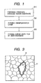
- a single-crystal silicon substrate which has been heat-treated in a reducing atmosphere containing hydrogen (hereinafter referred to as "hydrogen-annealed") is prepared (S1).
- An ion-implantation layer is formed by implanting oxygen ions into the single-crystal silicon substrate (S2).
- a buried oxide (BOX) layer is formed in the single-crystal silicon substrate by heat-treating the single-crystal silicon substrate in desired conditions (S3).
- An SIMOX wafer according to the present invention is obtained in this way.
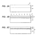
- a single-crystal silicon substrate 21 having a surface layer 22 which has been heat-treated in a reducing atmosphere containing hydrogen is prepared as shown in Fig. 2A .
- the surface layer is a less defective layer in which the grown-in defects such as COPs peculiar to a bulk wafer and defects such as OSF are remarkably reduced (the surface layer 22 may hereinafter be referred to as "less defective layer 22").
- the above-mentioned surface layer in single-crystal substrate 21 is a layer the number of COP or FPD or OSF in which is smaller than that in another portion of the same substrate.
- the surface layer 22 which has been hydrogen-annealed is clearly divided from another region 23 in Fig.
- a reference numeral 63 in Figs. 6A through 6D , a reference numeral 83 in Figs. 8A through 8F , a reference numeral 93 in Figs. 9A through 9E and a reference numeral 123 in Figs. 10A through 10D also represent regions, like the region 23 shown in Figs. 2A through 2C , which are other than surface layers formed on substrates.
- an ion-implantation layer 24 is formed as shown in Fig. 2B by implanting oxygen ions.
- a buried oxide film (BOX) layer 25 is formed by performing a desired heat-treatment ( Fig. 2C ).
- An SOI substrate 27 which has a single-crystal silicon layer (SOI layer) 26 on the BOX layer 25 is obtained in this way.
- the present invention makes it possible to obtain a high quality SIMOX wafer which has no defects such as COPs on a surface and in an interior of the SOI layer 26 or contains such defects in a number remarkably smaller than that of defects in an ordinary bulk wafer.
- the defects such as COP, FPD and OSF peculiar to the bulk wafer are inherent in a CZ wafer which is ordinarily used to manufacture an SIMOX wafer. Though the causes for these defects have not been clarified yet, it has been reported that each of the defects is strongly correlated to a concentration of oxygen contained in a wafer, and the defects such as COP and OSF are liable to be produced at high oxygen concentrations (for example, in "Problems on Silicon Crystal Wafers" (Realize Co., Ltd.) p. 55).
- the OSF oxidation induced stacking faults
- the OSF is produced from a fine defect which is introduced as a nucleus of crystal wafer during its growth and made visible at an oxidation step.
- a ring-like OSF may be observed, for example, when a wafer surface is subjected to wet oxidation.
- the COP and FPD which are observable without a heat-treatment are considered as defects attributable to the same cause and, though both these defects are not defined strictly, it is the case that the COP means an etch pit which is detectable with a fine particle detector or a foreign matter detector utilizing light scattering after wetting a wafer in SC-1 (NH 4 OH/H 2 O 2 ) solution which is one of element solution of an RCA cleaning solution, and that FPD means an etch pit which is observed through an optical microscope after wetting a wafer in a Secco solution (K 2 Cr 2 O 7 /HF/H 2 O) for about 30 minutes.
- SC-1 NH 4 OH/H 2 O 2
- FPD means an etch pit which is observed through an optical microscope after wetting a wafer in a Secco solution (K 2 Cr 2 O 7 /HF/H 2 O) for about 30 minutes.
- the present invention forms the SOI layer 26 itself so as to have no or a remarkably reduced number of defects such as COP since it forms the surface layer 22 in which the defects such as COP described above disappear or are reduced by annealing the surface of the silicon substrate with hydrogen and then forms the BOX layer 25 by implanting oxygen ions into the silicon substrate.
- reference numerals 31 and 32 represent the COP and a silicon atom which are schematically shown respectively.
- Reference numeral 33 represents an oxide film.
- an oxide film 33 of several nanometer thick exists on an inside wall of the COP 31.
- the oxide film 33 is removed by a reducing function of hydrogen, and a defective portion is gradually buried due to rearrangement of Si atoms and the COP 31 finally disappears ( Denshi-Zairyou(Electronic Materials), June, pp. 22 - 26 (1998 ).
- Japanese Patent Application Laid-Open No. 10-41241 discloses a hydrogen-annealing which is effected after forming the BOX layer 105.
- a temperature for the hydrogen-annealing is within a range between 800°C and 1000°C which is not lower than a temperature at which oxygen between lattices of the SOI layer 106 is reduced and not higher than a temperature at which reduction does not proceed to an oxide film on an interface of the BOX layer 105.
- Fig. 4 is an enlarged view of a region 114 shown in Fig. 11B .
- oxygen ions are distributed within a rather broad range around a center (49 in Fig. 4 ) of a projection range R p .
- oxygen existing in regions at which oxygen concentrations are low collected around the center 49 of the projection range R p at which oxygen concentration is high, thereby contracting the distribution smaller than that before the heat-treatment.
- Densities of slashes in Fig. 4 schematically represent concentrations of oxygen.
- Fig. 4 shows oxygen concentrations which are lowered from the center 49 of the projection range R p .
- COPs 41 exist in the vicinities of the ion-implantation layer 104, however, oxygen ions are collected around not only the center 49 of the projection range R p but also the COPs 41. Accordingly, COPs 51 are grown larger than those before forming a BOX layer 55 ( Fig. 5 ). This growth is considered due to a fact that the COPs have oxide films on their inside walls as described above and make their internal oxygen concentrations higher than those in surroundings.
- the COPs 51 grow large in the vicinities of the BOX layer 55 in particular, thereby being hardly removable.
- Japanese Patent Application Laid-Open No. 64-72633 and No. 8-46161 disclose a heat-treatment which is performed to form the BOX layer 105 not in an argon-oxygen mixture gas but in a hydrogen gas atmosphere after implanting oxygen ions into the silicon substrate.
- oxygen which can contribute to the formation of the BOX layer 105 is also reduced and finally removed when the wafer is hydrogen-annealed as an attempt to vanish COPs existing in the vicinities of an interface of the BOX layer 105.
- oxygen to be used for forming the BOX layer is lost as the COPs disappear, whereby the BOX layer may be thin.
- a silicon substrate is hydrogen-annealed before oxygen ions are implanted into the silicon substrate.
- an MCZ silicon wafer is preferably usable as a silicon substrate to be hydrogen-annealed. It has been reported that the MCZ method is capable for manufacturing a wafer while suppressing enlargement of COPs contained in silicon more effectively than the CZ method (Denshi-Zairyou(Electronic Materials), June (1998), p. 22). By annealing the MCZ silicon wafer with hydrogen, it is possible to form a less defective layer 22 which has a quality higher than that of a less defective layer obtained by annealing the CZ wafer with hydrogen.
- the lowering of the oxygen concentrations improves a quality of a surface layer of the wafer, thereby permitting forming a surface layer 22 which has a smaller number of defects such as COPs and OSFs (the surface layer may hereafter be referred to as "less defective layer").
- the CZ silicon wafer contains COPs at a density of 10 5 to 10 7 /cm 3 and an 8-inch CZ wafer, for example contains COPs in a number of 400 to 500 COPs per unit wafer in the vicinity of its surface.
- the CZ silicon wafer is hydrogen-annealed, however, the number of COPs is remarkably reduced to 10 or so in the vicinity of the surface. That is, a substantially defectless layer (DZ layer; Denuded Zone) is formed.
- DZ layer Denuded Zone
- the expression "the number per unit wafer” means herein the number of COPs or the like per area to be occupied by a wafer. In case of the 8-inch wafer, the number per unit wafer is the number of COPs in an area of about 324 cm 2 .
- the less defective layer 22 formed by the hydrogen-annealing so as to have thickness on the order of 500 to 5000 mm.
- An oxygen concentration in the less defective layer 22 is not higher than 1 ⁇ 10 18 atoms/cm 3 , preferably not higher than 5 ⁇ 10 17 atoms/cm 3 , more preferably not higher than 1 ⁇ 10 17 atoms/cm 3 .
- the COP density per unit volume in the less defective layer 22 is not higher than 5 ⁇ 10 6 /cm 3 , preferably not higher than 1 ⁇ 10 6 /cm 3 , more preferably not higher than 1 ⁇ 10 5 /cm 3 . It is desirable in particular that a COP density in a depth region from an outermost surface of the surface layer 22 to a projection range of the implanted ions is within the range specified above.
- the number of COPs per unit wafer in the less defective layer 22 is not larger than 500, preferably not larger than 100, more preferably not larger than 50, further more preferably not larger than 10. It is desirable in particular that the number of COPs per unit wafer on the surface of the wafer is not larger than 100 specified above. Since COPs are distributed on a surface of a wafer
- the number per unit wafer means "the number per wafer area” and in case of the 8-inch wafer, for example, it is the number of COPs per about 324 cm 2 .
- the number per unit area of a wafer surface is not larger than 1.6/cm 2 , preferably not larger than 0.5/cm 2 , and more preferably not larger than 0.05/cm 2 .
- the number of FPDs per unit area of the less defective layer 22 is not larger than 5 ⁇ 10 2 /cm 2 , more preferably not larger than 1 ⁇ 10 2 /cm 2 .
- a density of OSFs per unit area is not higher than 100/cm 2 , preferably not higher than 50/cm 2 , more preferably not higher than 10/cm 2 .
- the reducing atmosphere containing hydrogen which is to be used for heat-treatment to form the less defective layer 22 may be composed of a 100% gas of hydrogen, a mixture gas of hydrogen and rare gas (such as Ar, He, Ne, Xe or Kr) or a mixture gas of hydrogen and nitrogen.
- a mixture gas of hydrogen and rare gas such as Ar, He, Ne, Xe or Kr
- a mixture gas of hydrogen and nitrogen such as Ar, He, Ne, Xe or Kr
- the hydrogen-annealing at a temperature which is not lower than 500°C and not higher than a melting point of the silicon substrate, preferably not lower than 800°C and not higher than the melting point of the silicon substrate, more preferably not lower than 1000°C and not higher than the melting point of the silicon substrate.
- the hydrogen-annealing at a temperature of higher than 1000°C and less than the melting point of the silicon brings about a large advantageous effect of decreasing steeply COPs and so forth.
- the melting point of silicon is approximately 1412°C.
- the annealing temperature is set at a level which is not lower than 800°C and not higher than 1350°C. More preferably, the annealing temperature is higher than 1000°C and not higher than 1350°C.
- a pressure of the atmosphere containing hydrogen for the hydrogen-annealing may be at an atmospheric level, a reduced level or an enhanced level, it is preferable that atmosphere is kept at the atmospheric level (1 ⁇ 10 5 Pa) or a level which is not higher than the atmospheric level and not lower than 1 ⁇ 10 4 Pa. It is also preferable to perform the hydrogen-annealing at a lightly reduced level of the atmospheric pressure -100 mm Hg. Defects such as the COPs caused by outward diffusion of oxygen can be reduced effectively by performing the hydrogen-annealing at a reduced pressure though the effect is dependent on a structure of a furnace used for the heat-treatment.
- An ordinary vertical type heat-treatment furnace or a horizontal type heat-treatment furnace may be used for the hydrogen-annealing.
- the furnace may use an electrical resistance heater, a high-frequency heater or the like.
- the hydrogen-annealing may be carried out by utilizing radiation from a lamp which is used for RTA (Rapid Thermal Annealing).
- a lamp which is used for RTA Rapid Thermal Annealing
- an infrared light annealing apparatus using a halogen lamp or an arc lamp, a flash lamp annealing apparatus using a xenon flash lamp or the like may be used as a rapid annealing apparatus.
- a lamp used for heating in particular makes it possible to carry out the hydrogen-annealing in a short time.
- the hydrogen-annealing can be carried out for several seconds to tens of hours, preferably several seconds to several hours.
- a silicon oxide layer on the silicon substrate 21 by oxidizing a surface of the surface layer 22 so that oxygen ions are implanted from the side of the silicon oxide layer.
- Thermal oxidizing such as the following concrete means is employed as the above-mentioned oxidizing:
- a protective layer may be formed by depositing a silicon oxide film or a silicon nitrogen film on the surface layer 22 by a CVD method such as a heat CVD method or a plasma CVD method.
- the protective layer has thickness of several nanometers to several micrometers.
- the ion-implantation layer 24 is located inside the less defective layer 22 in Figs. 2A through 2C , the ion-implantation layer 24 may be located on an interface between the surface layer 22 and the region 23 so far as a single-crystal silicon layer functioning as the SOI layer 26 is a less defective layer.
- the region 23 occupies all portions of the silicon substrate which are other than a region (a surface layer 22) which is made into a less defective layer by the hydrogen-annealing. It is desirable to implant ions so that the projection range R p (implantation depth) of the ions is located inside the surface layer 22 shown in Fig. 2A .
- an entire range, an upper surface or a bottom surface of the silicon substrate is formed as the less defective layer 22.
- An ion-implantation layer 124 may be formed, for example, as shown in Figs. 10A through 10D .
- An embodiment of the present invention will be exemplified briefly with reference to Figs. 10A through 10D .
- a substrate 121 composed of a single-crystal Si wafer is prepared as an Si substrate and at least a main surface of the substrate is heat-treated in an atmosphere containing hydrogen, thereby forming a surface layer 122 which has a reduced number of defects due to bulk.
- the surface layer 122 is traced as if it is clearly separated from the rest portion of the substrate 121 with a border, the surface layer 122 gradually changes actually.
- an insulating layer 128 functioning as a protective layer may be formed on the surface layer 122 as occasion demands ( Fig. 10A ).
- oxygen ions are implanted from the side of the main surface, i.e., the surface layer 122, of the substrate 121.
- the ion-implantation layer 124 is formed in the vicinity of an interface between a low region 123 of the substrate 121 and the surface layer 128 or inside the surface layer 122.
- an implantation energy and an implanting rate are adjusted so that interface between the heat-treated surface layer 122 and the low region 123 is included in a silicon oxide layer when the ion-implantation layer 124 becomes a silicon oxide layer after a heat-treatment and ions are implanted in the adjusted conditions of the implantation energy and implanting rate ( Fig. 10B ).
- the substrate 121 is heat-treated as shown in Fig. 10C .
- a silicon oxide layer (buried silicon oxide layer) 125 is thus formed under the single-crystal silicon layer 122 which is located on a side of the main surface of the substrate 121.
- a semiconductor substrate (SIMOX wafer) is obtained as shown in Fig. 10D .
- the surface oxide film 128 may not be removed till a stage immediately before a device processing step in order to prevent the surface from being contaminated.
- the single-crystal silicon layer 122 thus obtained is flattened and uniformly thinned by way of the silicon oxide layer 125, thereby being formed so as to have a large area over the entire range of the wafer.
- the semiconductor substrate thus obtained is usable preferably to manufacture an insulated electronic element.
- the semiconductor substrate may be heat-treated once again in a reducing atmosphere containing hydrogen as occasion demands. Surface roughness is smoothed by these heat-treatments. The heat-treatment produces no slight scratches on the surface since it can smooth the surface without touch polishing which has a mechanical polishing function stronger than a chemical etching function.
- oxygen ions can be implanted at an accelerating voltage within a range from 1 keV to 10 MeV
- thickness of an ion-implantation layer changes dependently on levels of accelerating voltages and it is preferable to select an accelerating voltage on the order of several tens keV to 500 keV.
- An implantation radiation dose is 1.0 ⁇ 10 16 /cm 2 to 1.0 ⁇ 10 19 /cm 2 , more preferably within a range from 5.0 ⁇ 10 16 /cm 2 to 5.0 ⁇ 10 18 /cm 2 .
- oxygen ions are implanted at a temperature within a range from -200°C to 700°C, preferably within a range from 0°C to 700°C, more preferably within a range from a room temperature to 700°C.
- a temperature of the substrate during the ion-implantation is 550°C through 650°C so as to obtain a suitable buried oxide film with small electric current leak.
- oxygen ions into a silicon substrate it is ordinary to select only oxygen ions (O + ) out of various kinds of ions emitted from an ion source with a mass separating apparatus, accelerate the selected O + ions at a desired accelerating voltage and implant the ions into a silicon substrate with an ion beam obtained by the acceleration.
- O + oxygen ions
- To implant the ions into an entire surface of the substrate ions are implanted while scanning the silicon substrate with the ion beam. Needless to say, this method is not limitative of the present invention.
- This method is configured not to project an ion beam but to irradiate a large area at a time, thereby permitting to shorten a time required for implanting oxygen ions but reducing a manufacturing cost of a semiconductor substrate.
- this method is capable of implanting nitrogen ions in place of oxygen ions when a silicon nitride layer is required in place of a silicon oxide layer as an insulating layer for an SOI substrate.
- ions are implanted at a plurality of steps while changing an implantation radiation dose and/or an implantation energy (an accelerating voltage).
- an implantation energy is to be changed, it is preferably to select an implantation energy level for a second step which is lower than that at a first step.
- ions are to be implanted at a plurality of steps, it is possible to select different kinds of ions to be implanted into a silicon substrate at different steps.
- ions are to be implanted at two steps, it is preferable to implant a first kind of ions and then a second kind of ions which are lighter than the first kind of ions.
- oxygen ions and hydrogen ions are to be selected as the first and second kinds respectively.
- a protective layer is not formed on an uppermost surface of a silicon substrate before forming the ion-implantation layer, it is also preferable to form a protective layer on a surface of a silicon substrate after an ion-implantation layer is formed.
- the protective layer is capable of preventing the surface of the substrate from being roughened by a high temperature heat-treatment at a stage to form the BOX layer.
- a heat-treatment atmosphere to form the BOX layer which is the buried oxide film is an atmosphere consisting mainly of a gas selected from among oxygen, nitrogen, Ar, He, Ne and Xe, more preferably a gas atmosphere prepared by diluting oxygen with an inert gas (for example, a mixture gas atmosphere of argon and oxygen).
- the BOX layer can be formed by heat-treatment in a reducing atmosphere containing hydrogen.
- a heat-treatment temperature to form the BOX layer is a temperature which is not lower than 600°C and not higher than a melting point of silicon, preferably not lower than 800°C and not higher than the melting point of silicon, more preferably not lower than 1000°C and not higher than 1400°C.
- a temperature which is not lower than 800°C and not higher than 1000°C it is preferable to select a temperature which is not lower than 800°C and not higher than 1000°C.
- a heat-treatment time to form the BOX layer is not shorter than 0.5 hour and not longer than 20 hours, preferably not shorter than 2 hours and not longer than 10 hours. Though a heat-treatment time as short as possible is preferable to lower a manufacturing cost, it is desired to specify a heat-treatment time so as to form a uniform and continuous BOX layer.
- the BOX layer can be formed under an atmospheric pressure, a reduced pressure or an enhanced pressure.
- An SOI substrate is obtained by forming the BOX layer and when the SOI layer 26 has a rough surface, it is preferable to smooth the surface of the SOI layer after removing the surface oxide film.
- the surface of the SOI layer is smoothed by chemical-mechanical polishing (CMP) or hydrogen-annealing.
- CMP chemical-mechanical polishing
- abrasive materials for the CMP are polishing grains of a borosilicate glass, titanium dioxide, titanium nitride, aluminium oxide, iron nitrate, cerium oxide, colloidal silica, silicon nitride, silicon carbide, graphite and diamond or abrasive grain liquid consisting of these polishing grains and an oxidizing agent such as H 2 O 2 or KIO 3 and an alkaline solution such as NaOH or KOH.
- the surface of the SOI layer can be smoothed by hydrogen-annealing in an atmosphere consisting a 100% gas of hydrogen or a mixture gas of hydrogen and a rare gas (Ar, Ne or the like).
- the hydrogen-annealing allows boron and phosphorus to be diffused out of the SOI layer, thereby enhancing resistance of the SOI layer.
- a temperature for the hydrogen-annealing is not lower than 800°C and not higher than melting point of silicon, preferably not lower than 800°C and not higher than 1350°C, more preferably not lower than 850°C and not higher than 1250°C.
- the atmosphere containing hydrogen for the hydrogen-annealing may be kept at an atmospheric pressure or a reduced pressure, it is preferable to carry out the annealing at an atmospheric pressure (1 ⁇ 10 5 Pa) or a pressure which is lower than the atmospheric pressure and not lower than 1 ⁇ 10 4 Pa.
- a slightly reduced pressure on the order of the atmospheric pressure -100 mm Hg is more preferable for the hydrogen-annealing.
- the protective layer is removed as occasion demands after the BOX layer 25 is formed.
- the protective layer is removed by polishing, grinding,
- CMP dry etching or wet etching
- an etchant is fluoro-nitride series, enthylenediamine series, KOH series or hydrazine series etchant.
- an etchant is hydrofluoric acid, a mixture liquid of hydrofluoric acid to which at least either of hydrogen peroxide and alcohol is added or a mixture liquid of buffered hydrofluoric acid to which at least either of hydrogen peroxide and alcohol is added).
- the present invention makes it possible to enhance a yield of devices by reducing or vanishing COPs in SOI layers. Under the present circumstances where it is the that wafers which have larger diameters hereafter will make it more difficult to enhance qualities of crystals, it is considered that qualities of bulk wafers are to be lowered.
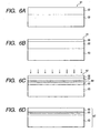
- a silicon substrate 61 is prepared and at least a main surface of the substrate is heat-treated in a reducing atmosphere containing hydrogen.
- the hydrogen-annealing forms a surface layer 62 which is a less defective layer which is free from defects such as COPs or has a remarkably small number of such defects ( Fig. 6A ).
- the protective layer 68 is, for example, a silicon oxide layer which is obtained by thermally oxidizing a surface of the surface layer 62. Needless to say, the protective layer 68 may be formed as occasion demands and omitted.
- An ion-implantation layer 64 is formed by implanting oxygen ions from the side of the main surface of the silicon substrate 61, i.e., from the side of the surface layer 62 ( Fig. 6C ). After adjusting an accelerating voltage and an implantation radiation dose, the ion implantation is performed so as to obtain a desired buried oxide film (BOX) layer.
- BOX buried oxide film
- the ion-implantation layer 64 is changed into a BOX layer 65 as shown in Fig. 6D .
- an SOI layer 66 which contains no defects such as the COPs (or contains the defects in a remarkably small number) can be obtained by removing the protective layer 68.
- the protective layer 68 may not be removed till a step immediately before processing a device to prevent contamination on the surface.
- An SIMOX wafer 67 is completed in this way.
- This wafer is preferably usable to manufacture an insulated electronic element.
- a single-crystal silicon substrate which has been hydrogen-annealed is prepared (S1). After forming a surface protective film on the single-crystal silicon substrate, an ion-implantation layer is formed by implanting oxygen ions into the single-crystal silicon substrate (S2). Then, a BOX layer is formed in the single-crystal silicon substrate by heat-treating the single-crystal silicon substrate in desired conditions (S3). These steps are similar to those in the flowchart shown in Fig. 1 . At the step (S2), the formation of the protective film may be omitted as occasion demands.
- the silicon substrate is cleaned (S4) after the BOX layer is formed in order to form an ion-implantation layer once again (S5). Then, a heat-treatment is carried out as at (S3) to form a BOX layer (S6). An SIMOX wafer is completed in this way (S7).
- S4 When particles exist on a surface of a substrate, the particles function as masks and the ion-implantation layer may not be formed at some regions.
- This embodiment is capable of preventing oxygen ions from being implanted ununiformly since it is configured to clean the surface of the silicon substrate after forming the BOX layer and then implant ions once again.
- the ion implantation step may be repeated at any times as occasion demands. Furthermore, it is preferable to clean the silicon substrate after the step (S1) and before the step (S2).
- the heat-treatment to form the BOX layer may be carried out at a single step after completing the final ion implantation step.
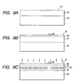
- a silicon substrate 81 hydrogen-annealed and having a surface layer 82 containing a remarkably small number of defects such as COPs is prepared ( Fig. 8A ).
- a protective layer 88 is formed on the surface layer 82 ( Fig. 8B ).
- a reference numeral 89 represents a particle adhering to the silicon substrate.
- the protective layer 88 is preferable to prevent a surface from being roughened by implanting ions but may not be formed as occasion demands.
- An ion-implantation layer 84 is formed as shown in Fig. 8C .
- the particle 89 functions as a mask, thereby producing a region in which the ion-implantation layer is not formed.
- the ion-implantation layer 84 is formed in the surface layer 82 in Fig. 8C , this location is not limitative needless to say.
- the BOX layer 85 is also made discontinuous under an influence due to the particle 89 ( Fig. 8D ).
- the silicon substrate 81 is cleaned to remove the particle 89 (not shown).
- an ion-implantation layer 74 is formed once again ( Fig. 8E ) and a BOX layer 75 is formed by carrying out a desired heat-treatment.
- An SIMOX wafer 87 which has a remarkably smooth SOI layer is completed by heat-treating a surface of an SOI layer 86 in a reducing atmosphere containing hydrogen after removing the surface protective layer 88 ( Fig. 8F ).
- DHF mixture solution of HF and H 2 O
- APM mixture solution containing NH 4 OH and H 2 O 2
- HPM mixture solution containing HCl and H 2 O 2
- SPM mixture solution containing H 2 SO 4 and H 2 O 2
- FPM mixture solution containing HF and H 2 O 2
- BHF mixture solution of NH 4 F, Hf and H 2 O
- Figs. 9A through 9E are schematic sectional views illustrating a third embodiment of the present invention.
- a silicon substrate 91 having a surface layer 92 which has been hydrogen-annealed and a protective layer 98 which is formed on the surface layer 92 is prepared ( Fig. 9A ).
- the protective layer 98 may be omitted as occasion demands.
- An ion-implantation layer 94 is formed by implanting oxygen ions from the side of the surface layer 98 as shown in Fig. 9B .
- a BOX layer 95 is formed by carrying out a desired heat-treatment ( Fig. 9C ).
- a desired heat-treatment Fig. 9C
- the protective layer 98 is removed as occasion demands and then the silicon substrate 91 is subjected to a high temperature heat-treatment, i.e., an ITOX treatment (Internal Thermal Oxidation) in an oxidizing atmosphere.
- a high temperature heat-treatment i.e., an ITOX treatment (Internal Thermal Oxidation) in an oxidizing atmosphere.
- the ITOX treatment not only forms a surface oxide film 99 once again on a surface of the SOI layer 92 but also thickens the internal BOX layer 95, thereby enhancing a reliability of the BOX layer ( Fig. 9D ).
- the removal of the protective layer 98 which is conducted prior to the ITOX treatment may be omitted.
- a protective layer may be formed after the ion-implantation layer 94 is formed.
- an atmosphere containing oxygen concretely an atmosphere consisting of oxygen and an inert gas (Ar, Ne or the like).
- the ITOX treatment can be carried out in an atmosphere kept at an atmospheric level, a reduced pressure or an enhanced pressure.
- An oxygen concentration in the atmosphere may be within a range from 1% to 100%.
- the ITOX treatment it is preferable to carry out the ITOX treatment at a temperature within a range from 1000°C to a level not higher than the melting point of silicon, preferably within a range from 1150°C to a level not higher than the melting point of silicon.
- a temperature not less than 1200°C, more preferably within a range between not less than 1300°C and not more than melting point of silicon.
- the protective layer 99 may not be removed till a step just before processing a device.
- Flatness of the SOI layer 92 can be enhanced by heat-treating it in a reducing atmosphere containing hydrogen after removing the surface oxide film 99.
- CZ wafers Two 8-inch single-crystal silicon substrates (CZ wafers) which were manufactured by the CZ method were prepared as silicon substrates.
- One of the substrates was heat-treated in a reducing atmosphere containing hydrogen. Treatment conditions were an atmosphere consisting 100% of hydrogen, 1200°C and two hours. The other substrate was not heat-treated for comparison.
- Oxygen ions are implanted with an accelerating energy of 180 keV and at a density of 1.5 ⁇ 10 18 cm -2 .
- the substrate was kept at a temperature of 550°C during the ion implantation.
- each substrate was heat-treated in an atmosphere of O 2 (10%)/Ar(90%) at 1350°C for four hours.
- Each substrate was completed as an SIMOX wafer (SOI wafer) of a single-crystal silicon semiconductor layer (SOI layer) 179 nm thick and a buried silicon oxide layer (BOX layer) 400 nm thick.
- SOI wafer SIMOX wafer
- SOI layer single-crystal silicon semiconductor layer
- BOX layer buried silicon oxide layer
- the SOI wafer was treated with an SC-1 cleaning liquid (a mixture liquid of 1.0 wt% of NH 4 OH, 6.0 wt% of H 2 O 2 and water) for ten minutes.
- the number of COPs (on the order of 0.1 to 0.2 pm) on the surface of the SOI wafer was counted using a surface particle detector (for example, SP-1 manufactured by KLA-Tencor Co., Ltd.)
- the inspection indicated 5 COPs per unit wafer for the SOI wafer manufactured using the silicon substrate the CZ wafer of which had been hydrogen-annealed before implantation of oxygen ions. In this way, it was possible to sufficiently reduce in the SOI wafer the number of COPs which are the defects attributable to the CZ-Si substrate.
- the surface particle detector indicated 250 COPs on the surface of the SOI wafer which had not been hydrogen-annealed and 7 COPs on the surface of the SOI wafer which had been hydrogen-annealed before implantation of oxygen ions.
- a protective layer by oxidizing a surface of an Si substrate before implantation of oxygen ions makes it possible to effectively prevent the surface from being roughened by implanting ions.
- a silicon oxide layer as a protective layer by thermally oxidizing a surface of a silicon substrate prior to formation of an ion-implantation layer.
- OSFs may be formed in a wafer and defects existing within a region to form an SOI layer produce influences on a final SOI layer when a silicon oxide layer is formed by thermally oxidizing an ordinary CZ wafer
- the present invention which is configured to oxidize a surface of the surface layer 22 having been hydrogen-annealed is capable of preventing OSFs from being produced. It is considered that this effect is obtained because an oxygen concentration on the surface of the substrate is lowered by annealing the silicon substrate with hydrogen prior to the formation of a protective layer.
- a CZ wafer was not hydrogen-annealed for comparison.
- Surface silicon oxide films 50 nm thick were formed by thermally oxidizing surfaces of surface layers of the silicon substrates subjected to the heat-treatments.
- the oxide films were formed to prevent the surfaces from being roughened by implanting ions. Needless to say, these oxide layers may not be formed as occasion demands.
- O + ions were implanted through the surface silicon oxide films at a density of 2 ⁇ 10 18 cm -2 at 180 keV.
- the ion implantation was conducted at a temperature of 550°C.
- the ion implantation there were formed surface layers which had a small number of defects as well as ion-implantation layers which had concentration peaks in the vicinities of interfaces between the surface layers and the original substrates.
- SOI wafers each consisting of single-crystal silicon semiconductor layer (SOI layer) 150 nm/buried silicon oxide layer 400 nm were completed.
- the SOI wafers were treated with an SC-1 cleaning liquid (a mixture liquid consisting of 1.0 wt% of NH 4 OH, 6.0 wt% of H 2 O 2 and water) for ten minutes.
- the numbers of COPs on surfaces of the SOI wafers was counted with a surface particle detector (for example, SP-1 manufactured by KLA-Tencor Co., Ltd.).
- the number of COPs on the SOI wafers treated in the conditions (1) through (6) was not larger than 20 though the numbers was more or less variable.
- the conditions (3) in particular permitted to obtain an SOI wafer which had three COPs and was substantially free from defects such as COPs.
- a CZ-Si wafer which was heat-treated at 1200°C for two hours in 100% of hydrogen as in (2) in EXAMPLE 2 was prepared.
- O + ions were implanted through a surface silicon oxide layer to 2 ⁇ 10 17 cm -2 at 180 keV.
- the CZ wafer was kept at a temperature of 550°C during the ion implantation.
- a buried silicon oxide film thus formed had a thickness on the order of 100 nm.
- O + ions were implanted once again to 5 ⁇ 10 17 cm -2 at 180 keV and the wafer was subjected to a similar heat-treatment. The cleaning, ion implantation and heat-treatment were repeated until oxygen was implanted in a total amount of 2 ⁇ 10 18 cm -2 .
- the number of COPs on a surface of the SOI layer was measured as in EXAMPLE 1 and the measurement indicates COPs on the order of five per unit wafer, whereby the wafer was substantially free from defects such as COPs and FPDs attributable to the CZ-Si substrate.
- An Si wafer which had a small number of defects on a surface was prepared by heat-treating a CZ-Si wafer in a hydrogen atmosphere as in (2) of EXAMPLE 2.
- a silicon oxide film 20 nm thick was formed by thermal oxidation on a surface of a single-crystal silicon layer (SOI layer) which formed a surface of the wafer.
- SOI layer single-crystal silicon layer
- O + ions were implanted through the surface silicon oxide film to 4 ⁇ 10 17 cm -2 at 180 keV.
- the wafer was kept at a temperature of 550°C during the ion implantation.
- the ion-implantation layer was changed into a buried silicon oxide layer by heat-treating the substrate at 1350°C for four hours in an atmosphere of O 2 (10%)/Ar (90%).
- a wafer consisting of SOI layer 300 nm/buried silicon oxide layer 90 nm was completed in this way.
- the wafer was further heat-treated at 1350°C for four hours in an atmosphere of O 2 (70%)/Ar
- the SOI layer was a portion of a single-crystal silicon layer in which defects were reduced by the heat-treatment in the hydrogen atmosphere, the SOI wafer had defects such as COPs and FPDs on the order of five per unit wafer.
- An Si substrate was prepared by treating an Sb doped n type silicon wafer which had specific resistance of 0.005 ⁇ •cm (100) at 1200°C for two hours in 100% of hydrogen.
- a silicon oxide film 50 nm thick was formed by thermal oxidation on a surface of the substrate.
- O + ions were implanted through the silicon oxide film on the surface of the wafer to 4 ⁇ 10 17 cm -2 at 180 keV.
- the wafer was kept at a temperature of 550°C during the ion implantation.
- the SOI wafer was further heat-treated at 1350°C for four hours in an atmosphere of O 2 (70%)/Ar(90%). By removing the oxide film from the surface of the wafer, an SOI wafer consisting of SOI layer 200 nm/buried oxide film 120 nm was completed.
- the SOI layer of the SOI wafer was substantially free from defects such as COPs and FPDs which were attributable to a CZ-Si substrate.
- a P+ type Cz-Si wafer having specific resistance of 0.01 ⁇ •cm was prepared.
- the wafer was hydrogen-annealed by heat-treating at 1200°C for two hours in 100% of H 2 .
- an SiO 2 layer 50 nm thick was formed by thermal oxidation on a surface of the substrate.
- O + ions were implanted through the surface silicon oxide film to 2 ⁇ 10 18 cm -2 at 180 keV.
- the substrate was kept at a temperature of 550°C during the ion implantation.
- the substrate was heat-treated at 1350°C for four hours in an atmosphere of O 2 (10%)/Ar (90%).
- O 2 (10%)/Ar (90%) By removing the surface silicon oxide film, an SOI wafer consisting of SOI layer 150 nm/buried oxide film 400 nm was completed.
- the SOI layer was substantially free from defects such as COPs and FPDs which were attributable to the CZ-Si substrate.
- the SOI wafer was heat-treated in an atmosphere of 100% of highly pure hydrogen which was purified with a hydrogen refiner using palladium alloy (1100°C, 4 h).
- a boron concentration in the SOI wafer which was 2 ⁇ 10 18 /cm 3 before the heat-treatment was lowered to a level not higher than 5 ⁇ 10 15 /cm 3 after the heat-treatment in the SOI layer.
Landscapes
- Element Separation (AREA)
Claims (17)
- Verfahren zur Herstellung eines SOI-Substrats mit den folgenden Schritten:Vorbereiten eines einkristallinen Siliziumsubstrats, wobei zumindest eine Hauptoberfläche des Substrats Wasserstoff getempert ist, um eine weniger mit Defekten behaftete Schicht zu erzielen; Bilden einer ionenimplantierten Schicht, die sich innerhalb der weniger mit Defekten behafteten Schicht oder auf einer Schnittstelle zwischen der weniger mit Defekten behafteten Schicht und dem Substratbereich, der nicht die weniger mit Defekten behaftete Schicht ist, durch Implantieren von Sauerstoff-Ionen oder Stickstoff-Ionen in das einkristalline Siliziumsubstrat befindet;und Bilden eines vergrabenen Isolationsfilms durch Wärmebehandlung des einkristallinen Siliziumsubstrats, in dem die ionenimplantierte Schicht gebildet wird.
- Verfahren zur Herstellung eines SOI-Substrates nach Anspruch 1, wobei eine Schutzschicht auf der Hauptoberfläche des einkristallinen Siliziumsubstrats gebildet wird nachdem das einkristalline Siliziumsubstrat mittels Wasserstofftempern vorbereitet wurde und bevor die ionenimplantierte Schicht gebildet wird und Ionen von der Schutzschichtseite des Substrats implantiert werden.
- Verfahren zur Herstellung eines SOI-Substrates nach Anspruch 1 oder 2, wobei das vorbereitete einkristalline Siliziumsubstrat eine weniger mit Defekten behaftete Schicht auf seiner Oberfläche aufweist.
- Verfahren zur Herstellung eines SOI-Substrates nach Anspruch 3, wobei die weniger mit Defekten behaftete Schicht eine Schicht ist, die aus Kristallen stammende Partikel "COPs", oder Defekte im Flussverhalten "FDPs", oder durch Oxidation induzierte Stapelfehler "OSFs" in geringerer Anzahl als in anderen Bereichen des einkristallinen Siliziumsubstrats, aufweist.
- Verfahren zur Herstellung eines SOI-Substrates nach Anspruch 1 oder 2, wobei der Schritt des Vorbereitens des einkristallinen Siliziumsubstrats ein Schritt des Wärmebehandelns eines einkristallinen Siliziumsubstrats in einer reduzierenden Stickstoff enthaltenden Atmosphäre ist.
- Verfahren zur Herstellung eines SOI-Substrates nach Anspruch 5, wobei die reduzierende Stickstoff enthaltende Atmosphäre ein 100%iges Wasserstoffgas oder ein Gasgemisch aus Wasserstoff und einem Edelgas oder ein Gasgemisch aus Wasserstoff und Stickstoff ist.
- Verfahren zur Herstellung eines SOI-Substrates nach Anspruch 1 oder 2, wobei der Schritt des Vorbereitens bei einer Temperatur, die nicht niedriger als 800°C und nicht höher als der Schmelzpunkt von Silizium ist, durchgeführt wird.
- Verfahren zur Herstellung eines SOI-Substrates nach Anspruch 1 oder 2, wobei der Schritt des Vorbereitens bei einer Temperatur höher als 1000°C und nicht höher als der Schmelzpunkt von Silizium durchgeführt wird.
- Verfahren zur Herstellung eines SOI-Substrates nach Anspruch 1 oder 2 mit einem Schritt des Säuberns des einkristallinen Siliziumsubstrats vor Bilden der ionenimplantierten Schicht.
- Verfahren zur Herstellung eines SOI-Substrates nach Anspruch 1 oder 2, wobei das einkristalline Siliziumsubstrat ein CZ-Siliziumwafer ist.
- Verfahren zur Herstellung eines SOI-Substrates nach Anspruch 1 oder 2, wobei das einkristalline Siliziumsubstrat ein MCZ-Siliziumwafer ist.
- Verfahren zur Herstellung eines SOI-Substrates nach Anspruch 2, wobei die auf der Hauptoberfläche des einkristallinen Siliziumsubstrats gebildete Schutzschicht eine Siliziumoxidschicht oder eine Siliziumnitridschicht ist.
- Verfahren zur Herstellung eines SOI-Substrates nach Anspruch 1 oder 2, wobei die ionenimplantierte Schicht durch Implantieren der Ionen innerhalb eines Bereichs von 1,0 x 10¹⁶/cm2 bis 1,0 x 10¹⁹/cm2 gebildet wird.
- Verfahren zur Herstellung eines SOI-Substrates nach Anspruch 1 oder 2, wobei die ionenimplantierte Schicht durch einen Plasma-Immersions-Ionenimplantationprozess gebildet wird.
- Verfahren zur Herstellung eines SOI-Substrates nach Anspruch 1 oder 2, wobei das einkristalline Siliziumsubstrat in einer oxidierenden Atmosphäre nach Bilden des vergrabenen Isolationsfilms wärmebehandelt wird.
- Verfahren zur Herstellung eines SOI-Substrates nach Anspruch 1 oder 2, wobei das Siliziumsubstrat einer Oberflächenbehandlung nach Bilden des vergrabenen Isolationsfilms ausgesetzt wird.
- Verfahren zur Herstellung eines SOI-Substrates nach Anspruch 16, wobei die Oberflächenbehandlung Polieren, oder Wasserstofftempern einer Oberfläche des Siliziumsubstrats, oder eine Kombination daraus umfasst.
Applications Claiming Priority (4)
| Application Number | Priority Date | Filing Date | Title |
|---|---|---|---|
| JP17140298 | 1998-06-18 | ||
| JP17140298 | 1998-06-18 | ||
| JP15644299 | 1999-06-03 | ||
| JP15644299A JP3762144B2 (ja) | 1998-06-18 | 1999-06-03 | Soi基板の作製方法 |
Publications (2)
| Publication Number | Publication Date |
|---|---|
| EP0966034A1 EP0966034A1 (de) | 1999-12-22 |
| EP0966034B1 true EP0966034B1 (de) | 2009-11-25 |
Family
ID=26484193
Family Applications (1)
| Application Number | Title | Priority Date | Filing Date |
|---|---|---|---|
| EP99304716A Expired - Lifetime EP0966034B1 (de) | 1998-06-18 | 1999-06-16 | Verfahren zur Herstellung eines Silizium-auf-Isolator-Substrats |
Country Status (7)
| Country | Link |
|---|---|
| US (1) | US6313014B1 (de) |
| EP (1) | EP0966034B1 (de) |
| JP (1) | JP3762144B2 (de) |
| KR (1) | KR100358638B1 (de) |
| CN (1) | CN1155065C (de) |
| DE (1) | DE69941652D1 (de) |
| TW (1) | TW468278B (de) |
Families Citing this family (49)
| Publication number | Priority date | Publication date | Assignee | Title |
|---|---|---|---|---|
| JP3211233B2 (ja) * | 1998-08-31 | 2001-09-25 | 日本電気株式会社 | Soi基板及びその製造方法 |
| US6248642B1 (en) * | 1999-06-24 | 2001-06-19 | Ibis Technology Corporation | SIMOX using controlled water vapor for oxygen implants |
| JP2001144275A (ja) | 1999-08-27 | 2001-05-25 | Shin Etsu Handotai Co Ltd | 貼り合わせsoiウエーハの製造方法および貼り合わせsoiウエーハ |
| KR100730806B1 (ko) * | 1999-10-14 | 2007-06-20 | 신에쯔 한도타이 가부시키가이샤 | Soi웨이퍼의 제조방법 및 soi 웨이퍼 |
| TW587332B (en) | 2000-01-07 | 2004-05-11 | Canon Kk | Semiconductor substrate and process for its production |
| KR100545990B1 (ko) * | 2000-06-02 | 2006-01-25 | 주식회사 실트론 | 실리콘웨이퍼 내의 금속 불순물 제거 방법 |
| JP2002075917A (ja) * | 2000-08-25 | 2002-03-15 | Canon Inc | 試料の分離装置及び分離方法 |
| US6461933B2 (en) * | 2000-12-30 | 2002-10-08 | Texas Instruments Incorporated | SPIMOX/SIMOX combination with ITOX option |
| JP2002289552A (ja) * | 2001-03-28 | 2002-10-04 | Nippon Steel Corp | Simox基板の製造方法およびsimox基板 |
| JP2002289820A (ja) * | 2001-03-28 | 2002-10-04 | Nippon Steel Corp | Simox基板の製造方法およびsimox基板 |
| DE10131249A1 (de) * | 2001-06-28 | 2002-05-23 | Wacker Siltronic Halbleitermat | Verfahren zur Herstellung eines Films oder einer Schicht aus halbleitendem Material |
| US6555451B1 (en) * | 2001-09-28 | 2003-04-29 | The United States Of America As Represented By The Secretary Of The Navy | Method for making shallow diffusion junctions in semiconductors using elemental doping |
| US20030134486A1 (en) * | 2002-01-16 | 2003-07-17 | Zhongze Wang | Semiconductor-on-insulator comprising integrated circuitry |
| US6506654B1 (en) * | 2002-03-26 | 2003-01-14 | Advanced Micro Devices, Inc. | Source-side stacking fault body-tie for partially-depleted SOI MOSFET hysteresis control |
| JP4376490B2 (ja) * | 2002-07-19 | 2009-12-02 | 富士通マイクロエレクトロニクス株式会社 | 半導体装置の製造方法 |
| JP2004119943A (ja) * | 2002-09-30 | 2004-04-15 | Renesas Technology Corp | 半導体ウェハおよびその製造方法 |
| WO2004040633A1 (en) * | 2002-10-25 | 2004-05-13 | Intersurface Dynamics, Inc. | Method for using additives in the caustic etching of silicon for obtaining improved surface characteristics |
| TW200428637A (en) * | 2003-01-23 | 2004-12-16 | Shinetsu Handotai Kk | SOI wafer and production method thereof |
| EP1596437A4 (de) * | 2003-02-19 | 2009-12-02 | Shinetsu Handotai Kk | Verfahren zur herstellung eines soi-wafers und soi-wafer |
| JP4854917B2 (ja) * | 2003-03-18 | 2012-01-18 | 信越半導体株式会社 | Soiウェーハ及びその製造方法 |
| FR2857895B1 (fr) * | 2003-07-23 | 2007-01-26 | Soitec Silicon On Insulator | Procede de preparation de surface epiready sur films minces de sic |
| US6911376B2 (en) * | 2003-10-01 | 2005-06-28 | Wafermasters | Selective heating using flash anneal |
| US7473656B2 (en) * | 2003-10-23 | 2009-01-06 | International Business Machines Corporation | Method for fast and local anneal of anti-ferromagnetic (AF) exchange-biased magnetic stacks |
| EP1676311A1 (de) | 2003-10-24 | 2006-07-05 | Sony Corporation | Verfahren zur herstellung eineshalbleitersubstrats und halbleitersubstrat |
| JP2005210062A (ja) * | 2003-12-26 | 2005-08-04 | Canon Inc | 半導体部材とその製造方法、及び半導体装置 |
| CN100433257C (zh) | 2004-01-15 | 2008-11-12 | 野田优 | 制造单晶薄膜的方法 |
| US7718009B2 (en) * | 2004-08-30 | 2010-05-18 | Applied Materials, Inc. | Cleaning submicron structures on a semiconductor wafer surface |
| DE102005007599B3 (de) * | 2005-02-18 | 2006-05-11 | Infineon Technologies Austria Ag | Verfahren zur Herstellung einer Feldstoppzone |
| US7244659B2 (en) * | 2005-03-10 | 2007-07-17 | Micron Technology, Inc. | Integrated circuits and methods of forming a field effect transistor |
| US20060228492A1 (en) * | 2005-04-07 | 2006-10-12 | Sumco Corporation | Method for manufacturing SIMOX wafer |
| EP1909309A4 (de) * | 2005-07-22 | 2010-10-20 | Sumco Corp | Verfahren zur herstellung eines simox-wafers und durch ein solches verfahren hergestellter simox-wafer |
| JP2007266059A (ja) * | 2006-03-27 | 2007-10-11 | Sumco Corp | Simoxウェーハの製造方法 |
| JP5157075B2 (ja) * | 2006-03-27 | 2013-03-06 | 株式会社Sumco | Simoxウェーハの製造方法 |
| JP2008004821A (ja) * | 2006-06-23 | 2008-01-10 | Sumco Corp | 貼り合わせウェーハの製造方法 |
| US7557002B2 (en) * | 2006-08-18 | 2009-07-07 | Micron Technology, Inc. | Methods of forming transistor devices |
| US7989322B2 (en) | 2007-02-07 | 2011-08-02 | Micron Technology, Inc. | Methods of forming transistors |
| RU2373604C1 (ru) * | 2008-05-27 | 2009-11-20 | Валерий Филиппович Реутов | Способ формирования полной диэлектрической изоляции элементов в полупроводнике |
| JP5700617B2 (ja) | 2008-07-08 | 2015-04-15 | 株式会社半導体エネルギー研究所 | Soi基板の作製方法 |
| US7927975B2 (en) * | 2009-02-04 | 2011-04-19 | Micron Technology, Inc. | Semiconductor material manufacture |
| JP2012104808A (ja) * | 2010-10-14 | 2012-05-31 | Dainippon Screen Mfg Co Ltd | 熱処理装置および熱処理方法 |
| CN102586886A (zh) * | 2012-03-10 | 2012-07-18 | 天津市环欧半导体材料技术有限公司 | 一种用于去除硅晶片表面氧沉积物的硅晶片退火方法 |
| US20140130854A1 (en) * | 2012-11-12 | 2014-05-15 | Samsung Sdi Co., Ltd. | Photoelectric device and the manufacturing method thereof |
| KR102384962B1 (ko) | 2015-11-27 | 2022-04-11 | 에스케이하이닉스 주식회사 | 반도체 메모리 장치 |
| CN111470880A (zh) * | 2019-01-23 | 2020-07-31 | 元创绿能科技股份有限公司 | 具有多孔隙的离子交换膜及其制造方法 |
| JP7319059B2 (ja) | 2019-02-25 | 2023-08-01 | エア・ウォーター株式会社 | ペリクル中間体の製造方法およびペリクルの製造方法 |
| CN110006727A (zh) * | 2019-04-10 | 2019-07-12 | 深圳市锐骏半导体股份有限公司 | 一种离子注入机稳定性的监控方法 |
| CN112490113A (zh) * | 2020-11-12 | 2021-03-12 | 武汉新芯集成电路制造有限公司 | 一种半导体器件的制作方法 |
| CN115394707A (zh) * | 2021-05-24 | 2022-11-25 | 芯恩(青岛)集成电路有限公司 | 一种绝缘体上硅衬底及其制造方法及cmos器件制造方法 |
| CN113421849B (zh) * | 2021-06-09 | 2023-01-03 | 中环领先半导体材料有限公司 | 一种带绝缘埋层的硅衬底的制备工艺 |
Family Cites Families (12)
| Publication number | Priority date | Publication date | Assignee | Title |
|---|---|---|---|---|
| JPS62123098A (ja) | 1985-11-22 | 1987-06-04 | Toshiba Ceramics Co Ltd | シリコン単結晶の製造方法 |
| JPS6472533A (en) | 1987-09-11 | 1989-03-17 | Nippon Telegraph & Telephone | Manufacture of single crystal semiconductor substrate |
| US5310689A (en) | 1990-04-02 | 1994-05-10 | Motorola, Inc. | Method of forming a SIMOX structure |
| EP0553852B1 (de) | 1992-01-30 | 2003-08-20 | Canon Kabushiki Kaisha | Verfahren zur Herstellung eines Halbleitersubstrates |
| US5429955A (en) | 1992-10-26 | 1995-07-04 | Texas Instruments Incorporated | Method for constructing semiconductor-on-insulator |
| US5458755A (en) | 1992-11-09 | 1995-10-17 | Canon Kabushiki Kaisha | Anodization apparatus with supporting device for substrate to be treated |
| JP3036619B2 (ja) | 1994-03-23 | 2000-04-24 | コマツ電子金属株式会社 | Soi基板の製造方法およびsoi基板 |
| JPH0837286A (ja) | 1994-07-21 | 1996-02-06 | Toshiba Microelectron Corp | 半導体基板および半導体基板の製造方法 |
| JPH0846161A (ja) | 1994-07-29 | 1996-02-16 | Mitsubishi Materials Corp | Soi基板及びその製造方法 |
| DE19623791A1 (de) | 1996-06-14 | 1997-12-18 | Linde Ag | Verfahren zur Entfernung von Stickoxiden aus Gasen |
| US5989981A (en) | 1996-07-05 | 1999-11-23 | Nippon Telegraph And Telephone Corporation | Method of manufacturing SOI substrate |
| JPH1041241A (ja) | 1996-07-26 | 1998-02-13 | Sharp Corp | 半導体装置の製造方法 |
-
1999
- 1999-06-03 JP JP15644299A patent/JP3762144B2/ja not_active Expired - Fee Related
- 1999-06-14 US US09/332,102 patent/US6313014B1/en not_active Expired - Lifetime
- 1999-06-15 TW TW088110033A patent/TW468278B/zh not_active IP Right Cessation
- 1999-06-16 EP EP99304716A patent/EP0966034B1/de not_active Expired - Lifetime
- 1999-06-16 DE DE69941652T patent/DE69941652D1/de not_active Expired - Lifetime
- 1999-06-18 CN CNB991110749A patent/CN1155065C/zh not_active Expired - Fee Related
- 1999-06-18 KR KR1019990023076A patent/KR100358638B1/ko not_active Expired - Fee Related
Also Published As
| Publication number | Publication date |
|---|---|
| EP0966034A1 (de) | 1999-12-22 |
| DE69941652D1 (de) | 2010-01-07 |
| TW468278B (en) | 2001-12-11 |
| KR100358638B1 (ko) | 2002-10-25 |
| CN1155065C (zh) | 2004-06-23 |
| KR20000006300A (ko) | 2000-01-25 |
| JP2000077352A (ja) | 2000-03-14 |
| JP3762144B2 (ja) | 2006-04-05 |
| CN1241016A (zh) | 2000-01-12 |
| US6313014B1 (en) | 2001-11-06 |
Similar Documents
| Publication | Publication Date | Title |
|---|---|---|
| EP0966034B1 (de) | Verfahren zur Herstellung eines Silizium-auf-Isolator-Substrats | |
| US6350703B1 (en) | Semiconductor substrate and production method thereof | |
| JP4331593B2 (ja) | 半導体材料からなるフィルムまたは層およびフィルムまたは層の製造方法 | |
| EP1045448B1 (de) | Verfahren zur herstellung von einem soi-wafer mittels trennung durch wasserstoffimplantierung | |
| KR100402155B1 (ko) | 반도체기판의 제조방법, 반도체박막의 제조방법 및 다층구조 | |
| EP0955671B1 (de) | Verfahren zur Wiedergewinnung eines abgetrennten Wafers und zur Wiedergewinnung verwendeter Siliziumwafer | |
| EP1137069A1 (de) | Herstellungsverfahren für geklebten soi-wafer, und geklebter soi-wafer | |
| JP2006216826A (ja) | Soiウェーハの製造方法 | |
| JP4419147B2 (ja) | 貼り合わせウェーハの製造方法 | |
| JPWO2005024925A1 (ja) | Soiウェーハの作製方法 | |
| KR101071509B1 (ko) | 접합 웨이퍼 제조 방법 | |
| JP2009272471A (ja) | 貼り合わせウェーハの製造方法 | |
| JP2002184960A (ja) | Soiウェーハの製造方法及びsoiウェーハ | |
| JP4631347B2 (ja) | 部分soi基板およびその製造方法 | |
| US7582540B2 (en) | Method for manufacturing SOI wafer | |
| JP2004087768A (ja) | Soiウエーハの製造方法 | |
| JPH08236735A (ja) | Soi基板及びその製造方法 | |
| JP2009289948A (ja) | 貼り合わせウェーハの製造方法 | |
| JPH0878646A (ja) | 半導体基板及びその製造方法 | |
| JP5124973B2 (ja) | Soiウェーハの製造方法 | |
| JP2005286282A (ja) | Simox基板の製造方法及び該方法により得られるsimox基板 | |
| JPH1074918A (ja) | Soi基板及びその製造方法 | |
| JP2006032725A (ja) | 半導体ウェーハの酸化膜形成方法 | |
| JP2004087767A (ja) | Soiウエーハの製造方法 | |
| JP2005197525A (ja) | Soiウェーハの作製方法 |
Legal Events
| Date | Code | Title | Description |
|---|---|---|---|
| PUAI | Public reference made under article 153(3) epc to a published international application that has entered the european phase |
Free format text: ORIGINAL CODE: 0009012 |
|
| AK | Designated contracting states |
Kind code of ref document: A1 Designated state(s): DE FR GB IT NL |
|
| AX | Request for extension of the european patent |
Free format text: AL;LT;LV;MK;RO;SI |
|
| 17P | Request for examination filed |
Effective date: 20000508 |
|
| AKX | Designation fees paid |
Free format text: DE FR GB IT NL |
|
| 17Q | First examination report despatched |
Effective date: 20040615 |
|
| 17Q | First examination report despatched |
Effective date: 20040615 |
|
| GRAP | Despatch of communication of intention to grant a patent |
Free format text: ORIGINAL CODE: EPIDOSNIGR1 |
|
| GRAS | Grant fee paid |
Free format text: ORIGINAL CODE: EPIDOSNIGR3 |
|
| GRAA | (expected) grant |
Free format text: ORIGINAL CODE: 0009210 |
|
| AK | Designated contracting states |
Kind code of ref document: B1 Designated state(s): DE FR GB IT NL |
|
| REG | Reference to a national code |
Ref country code: GB Ref legal event code: FG4D |
|
| REF | Corresponds to: |
Ref document number: 69941652 Country of ref document: DE Date of ref document: 20100107 Kind code of ref document: P |
|
| REG | Reference to a national code |
Ref country code: NL Ref legal event code: VDEP Effective date: 20091125 |
|
| PG25 | Lapsed in a contracting state [announced via postgrant information from national office to epo] |
Ref country code: NL Free format text: LAPSE BECAUSE OF FAILURE TO SUBMIT A TRANSLATION OF THE DESCRIPTION OR TO PAY THE FEE WITHIN THE PRESCRIBED TIME-LIMIT Effective date: 20091125 |
|
| PLBE | No opposition filed within time limit |
Free format text: ORIGINAL CODE: 0009261 |
|
| STAA | Information on the status of an ep patent application or granted ep patent |
Free format text: STATUS: NO OPPOSITION FILED WITHIN TIME LIMIT |
|
| 26N | No opposition filed |
Effective date: 20100826 |
|
| REG | Reference to a national code |
Ref country code: FR Ref legal event code: ST Effective date: 20110228 |
|
| PG25 | Lapsed in a contracting state [announced via postgrant information from national office to epo] |
Ref country code: IT Free format text: LAPSE BECAUSE OF FAILURE TO SUBMIT A TRANSLATION OF THE DESCRIPTION OR TO PAY THE FEE WITHIN THE PRESCRIBED TIME-LIMIT Effective date: 20091125 |
|
| PG25 | Lapsed in a contracting state [announced via postgrant information from national office to epo] |
Ref country code: FR Free format text: LAPSE BECAUSE OF NON-PAYMENT OF DUE FEES Effective date: 20100630 |
|
| PGFP | Annual fee paid to national office [announced via postgrant information from national office to epo] |
Ref country code: GB Payment date: 20140610 Year of fee payment: 16 |
|
| PGFP | Annual fee paid to national office [announced via postgrant information from national office to epo] |
Ref country code: DE Payment date: 20140630 Year of fee payment: 16 |
|
| REG | Reference to a national code |
Ref country code: DE Ref legal event code: R119 Ref document number: 69941652 Country of ref document: DE |
|
| GBPC | Gb: european patent ceased through non-payment of renewal fee |
Effective date: 20150616 |
|
| PG25 | Lapsed in a contracting state [announced via postgrant information from national office to epo] |
Ref country code: DE Free format text: LAPSE BECAUSE OF NON-PAYMENT OF DUE FEES Effective date: 20160101 Ref country code: GB Free format text: LAPSE BECAUSE OF NON-PAYMENT OF DUE FEES Effective date: 20150616 |