EP0943925A2 - Elektro-optisches Abtast-Oszilloskop - Google Patents
Elektro-optisches Abtast-Oszilloskop Download PDFInfo
- Publication number
- EP0943925A2 EP0943925A2 EP99302013A EP99302013A EP0943925A2 EP 0943925 A2 EP0943925 A2 EP 0943925A2 EP 99302013 A EP99302013 A EP 99302013A EP 99302013 A EP99302013 A EP 99302013A EP 0943925 A2 EP0943925 A2 EP 0943925A2
- Authority
- EP
- European Patent Office
- Prior art keywords
- sampling
- data
- electro
- receiving light
- signal
- Prior art date
- Legal status (The legal status is an assumption and is not a legal conclusion. Google has not performed a legal analysis and makes no representation as to the accuracy of the status listed.)
- Withdrawn
Links
Images


Classifications
-
- G—PHYSICS
- G01—MEASURING; TESTING
- G01R—MEASURING ELECTRIC VARIABLES; MEASURING MAGNETIC VARIABLES
- G01R13/00—Arrangements for displaying electric variables or waveforms
- G01R13/20—Cathode-ray oscilloscopes
- G01R13/22—Circuits therefor
- G01R13/34—Circuits for representing a single waveform by sampling, e.g. for very high frequencies
- G01R13/347—Circuits for representing a single waveform by sampling, e.g. for very high frequencies using electro-optic elements
Definitions
- This invention relates to electro-optic sampling oscilloscopes that are used for observation of waveforms of measured signals which are detected by electro-optic sampling probes.
- electro-optic sampling oscilloscopes operate using electro-optic sampling probes (where the term of "electro-optic sampling” can be abbreviated by "EOS”) based on the known phenomena as follows:
- Electric fields are produced by measured signals and are connected with electro-optic crystals, on which laser beams are incident. Based on polarization states of the laser beams, it is possible to measure waveforms of the measured signals.
- sampling operations are performed on the measured signals under the condition where the laser beams are made in form of pulses, so it is possible to measure the waveforms with a very high resolution.
- EOS oscilloscopes have a variety of technical features and therefore attract attention to engineers, which is described in pp. 123-129 of the paper entitled “A High-Impedance Probe Based on Electro-Optic Sampling” written by Shinagawa and other members and published as the lectured monographs of the proceedings of 15 th Meeting of the Institute of Lightwave Sensing Technology under the names of the Institute of Applied Physics and Institute of Lightwave Sensing Technology on May of 1995.
- the features of the EOS oscilloscopes are as follows:
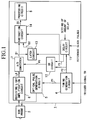
- FIG. 10 is a block diagram showing an example of a configuration of the EOS oscilloscope, which is basically constructed by a main body 1 and a EOS probe 2 for receiving light (beams) corresponding to measured signals.
- a trigger signal TR is a periodically varying signal which synchronizes with clock pulses for driving a measured circuit (not shown) which is subjected to measurement. Therefore, the measured circuit supplies the trigger signal TR to the main body 1.
- a timing generation circuit 4 Based on the trigger signal TR, a timing generation circuit 4 generates a pulse signal P1 for driving an optical pulse generation circuit 5 as well as a pulse signal P2 for driving an analog-to-digital converter (abbreviated by "A/D converter") 7.
- A/D converter analog-to-digital converter
- FIG. 11A is a time chart showing the trigger signal TR consisting of trigger pulses which periodically emerge;
- FIG. 11B is a time chart showing the pulse signal P1;
- FIG. 11C is a time chart showing the pulse signal P2.
- Each of pulses of the pulse signal P1 is delayed from each of the trigger pulses of the trigger signal TR in such a way that a delay time "st" therebetween is gradually increased.
- each of pulses of the pulse signal P2 is delayed from each of the trigger pulses of the trigger signal TR by a prescribed and fixed delay time "dt".
- the optical pulse generation circuit 5 receives the pulse signal P1 to generate optical pulses of laser beams, which are supplied to the EOS probe 2.
- a polarization state thereof changes in response to a signal at a probe contact portion of the measured circuit.
- the optical pulses whose polarization states are changed are converted to electric signals, which are supplied to a receiving light amplification circuit 6.
- the receiving light amplification circuit 6 amplifies output of the EOS probe 2 so as to produce a receiving light signal LS, which is then forwarded to the A/D converter 7.
- the A/D converter 7 performs sampling operations on the receiving light signal LS based on the pulse signal P2, so that the receiving light signal LS is subjected to analog-to-digital conversion.
- a processing circuit 8 performs a display process of measured waveforms based on digital output of the A/D converter 7.
- the aforementioned EOS oscilloscope suffers from a problem due to sampling of signals, as follows:
- the EOS oscilloscope At sampling, external noise is input to the receiving light amplification circuit. Or, the EOS oscilloscope inevitably performs sampling operations on low-frequency noise components such as the noise (e.g., shot noise, heat noise and 1/f noise) caused by the receiving light amplification circuit and the optical noise (e.g., noise components on light beams produced by LEDs). Therefore, performance of the EOS oscilloscope is deteriorated in S/N ratio.
- the noise e.g., shot noise, heat noise and 1/f noise
- the optical noise e.g., noise components on light beams produced by LEDs
- An electro-optic sampling oscilloscope (or EOS oscilloscope) of this invention is designed to perform measurement such that an electro-optic sampling probe (or EOS probe) is brought into contact with a measured circuit.
- Optical pulses are input to the EOS probe, wherein they are varied in polarization states in response to the measured circuit.
- an electric signal output from the EOS probe is amplified to produce a receiving light signal.
- the receiving light signal is subjected to sampling operations using a first pulse signal to produce detection data, while it is also subjected to sampling operations using a second pulse signal to produce noise data.
- the first pulse signal consists of pulses which emerge in synchronization with the optical pulses respectively, while the second pulse signal delays from the first pulse signal by a prescribed delay time.
- the EOS oscilloscope is capable of controlling a frequency band used for amplification as well as the delay time. For example, the delay time is made longer as the frequency band becomes narrower.
- measurement data are produced by subtracting the noise data from the detection data.
- the measurement data are processed so that a measured waveform representing a measurement result is displayed on a screen of the EOS oscilloscope.
- FIG. 1 is a block diagram showing a configuration of an EOS oscilloscope in accordance with an embodiment of the invention, wherein parts identical to those shown in FIG. 10 will be designated by the same reference symbols, hence, the description thereof will be omitted.
- a delay circuit 11 delays a pulse signal P2 (see FIG. 11C and FIG. 2C), output from the timing generation circuit 4, by a prescribed delay time so as to produce a pulse signal P3 (see FIG. 2D).
- the pulse signal P3 delays from the pulse signal P2 by a delay time Td, which is measured by counting a number of reference clock pulses which corresponds to a preset amount of delay.
- An OR circuit 12 performs a logical operation of "OR” on the pulse signals P2 and P3. So, the OR circuit 12 supplies the A/D converter 7 with a result of the logical operation of "OR", namely, a sampling pulse signal PS (see FIG. 2E).
- the A/D converter 7 converts a receiving light signal LS (see FIG. 2B), output from the receiving light amplification circuit 6, on the basis of the pulse signal PS so as to produce digital data D1 (see FIG. 2F).
- a latch circuit 13 latches such an output of the A/D converter 7 at the timing designated by the pulse signal P3. Then, the latch circuit 13 outputs data D2 (see FIG. 2G), which are forwarded to a subtraction circuit 14.
- the subtraction circuit 14 subtracts the output data D1 of the A/D converter 7 from the output data D2 of the latch circuit 13 to produce data D3 (see FIG. 2H), which are forwarded to the processing circuit 8.
- the timing generation circuit 4 sequentially outputs pulses of the pulse signal P1 shown in FIG. 2A, which is supplied to the optical pulse generation circuit 5.
- optical pulse generation circuit 5 Upon receipt of the pulse signal P1, optical pulse generation circuit 5 generates optical pulses using laser beams. So, the optical pulse generation circuit 5 outputs the optical pulses to the EOS probe 2. Every time the optical pulse passes through the EOS probe 2, it changes in polarization state in response to the measured signal.
- the optical pulses which are changed in polarization states are converted to electric signals, which are input to the receiving light amplification circuit 6.
- the receiving light amplification circuit 6 amplifies an output of the EOS probe 2 to produce a receiving light signal LS, which is forwarded to the A/D converter 7.
- FIG. 2B shows an example of a waveform of the receiving light signal LS.
- the timing generation circuit 4 When a prescribed time (e.g., 10 to 50 nanoseconds) elapses after the leading-edge timing of the pulse of the pulse signal P1, the timing generation circuit 4 outputs a pulse of the pulse signal P2 shown in FIG. 2C.
- This pulse P2 is supplied to the A/D converter 7 via the OR circuit 12 as a sampling pulse of the sampling pulse signal PS shown in FIG. 2E.
- the A/D converter 7 Upon receipt of the sampling pulses PS, the A/D converter 7 performs sampling operations on the receiving light signal LS, wherein sampled values are converted to digital data D1 shown in FIG. 2F.
- the pulse signal P2 is also delivered to the delay circuit 11, wherein it is delayed by a constant delay time Td and is then output as the pulse signal P3 shown in FIG. 2D.
- the delay time Td is set in such a way that a pulse P3 is output when the receiving light signal LS decreases to substantially zero level.
- the pulse P3 is supplied to the A/D converter 7 via the OR circuit 12 as a sampling pulse PS (see FIG. 2E). Upon receipt of such a sampling pulse PS corresponding to the pulse P3, the A/D converter 7 performs a sampling operation on the receiving light signal LS so as to convert it to digital data D1.
- the pulse signal P3 is also delivered to the latch circuit 13.
- the latch circuit 13 Upon receipt of the pulse signal P3, the latch circuit 13 latches an output of the A/D converter 7.
- values of the receiving light signal LS which are sampled at timings of pulses of the pulse signal P2 and are subjected to analog-to-digital conversion, are read by the latch circuit 13, which produces data D2 shown in FIG. 2G.
- the data D2 are forwarded to the subtraction circuit 14.
- the data D2 (see FIG. 2G) are produced by performing the sampling operation and analog-to-digital conversion on the receiving light signal LS at the timing of the pulse signal P2, so that the data D2 are output from the latch circuit 13 at the timing of the pulse signal P3.
- the A/D converter 7 outputs the data D1 (see FIG. 2F), which are produced by performing the sampling operation and analog-to-digital conversion on the receiving light signal LS at the timing of the pulse signal P3.
- the receiving light signal LS becomes substantially zero in level at the timing of the pulse signal P3.
- the data which are produced by sampling the receiving light signal LS at the timing of the pulse signal P3 are interpreted as noise data.
- the subtraction circuit 14 subtracts the output of the A/D converter 7 from the output of the latch circuit 13 to produce data D3 shown in FIG. 2H.
- the subtraction circuit 14 outputs the data D3 which are produced by subtracting the noise data from the data D2 corresponding to the receiving light signal LS.
- the data D3 are forwarded to the processing circuit 8, which in turn performs display of the measured signal(s).
- the present embodiment is designed in such a way that data are produced by subtracting the noise from the "sampled" receiving light signal LS, wherein the processing circuit 8 performs a display process based on such data whose noise is substantially eliminated.
- the circuit configuration of FIG. 1 is capable of eliminating low-frequency noise. That is, this circuit configuration is effective for elimination of the low-frequency noise shown in FIG. 2I, particularly, the noise whose level greatly changes in a lapse of time.
- FIG. 3 is a graph showing a relationship between noise frequency and noise reduction ratio with respect to the circuit configuration of FIG. 1.
- a characteristic curve L1 represents variations in decibel (dB) of the noise reduction ratio which is read in connection with a left axis
- a characteristic curve L2 represents variations in real number of the noise reduction ratio which is read in connection with a right axis.
- this graph of FIG. 3 is created and displayed based on values which are calculated with respect to the sample time difference of 125 nanoseconds.
- the position on time axis to latch the noise data i.e., the position of the pulse P3
- the A/D converter 7 should sample signal components in addition to noise components. For this reason, it is necessary to determine the delay time Td of the delay circuit 11 in such a way that the pulse P3 is located in proximity to the pulse P2 as closely as possible but the A/D converter 7 does not sample the signal components in addition to the noise components.
- Measured signal (e.g., EOS correction signal) which is known and which has a small amount of noise is applied to the EOS probe 2, so that measurement is performed while the delay time Td is sequentially changed. Based on the measurement result, it is possible to determine the delay time Td as a time value which has a best result in S/N ratio.
- the known techniques for detection of the S/N ratio and for setting of step changes of the delay time Td For example, the measured waveform is subjected to Fourier transform so that frequency components of the measured waveform are removed to produce a signal, which is then subjected to power measurement (or integration) so that noise is detected.
- intervals between the step changes of the delay time Td are varied by Newton method, for example.
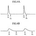
- the receiving light signal LS greatly changes in waveform by the frequency band employed by the receiving light amplification circuit 6.
- Preferable positions on the time axis for the pulses P2 and P3 are respectively shown in FIG. 4A and FIG. 4B. It can be observed from those figures that positions of the pulses P3 greatly change in response to the frequency bands of the receiving light amplification circuit 6.
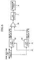
- a control circuit 31 is introduced to control the frequency band of the receiving light amplification circuit 6.
- the control circuit 31 there is provided a table whose content represents a relationship between band control data CF and delay control data CTd, wherein the band control data CF are used to control the frequency band of the receiving light amplification circuit 6 while the delay control data CTd are used to control the delay time of the delay circuit 11.
- the band control data CF are used to control the frequency band of the receiving light amplification circuit 6 while the delay control data CTd are used to control the delay time of the delay circuit 11.
- the present embodiment shown in FIG. 1 is designed such that the output of the receiving light amplification circuit 6 is subjected to analog-to-digital conversion and is then subjected to subtraction of the noise components by the subtraction circuit 14.
- the present embodiment can be modified such that as shown in FIG. 6, the receiving light amplification circuit 6 is followed by two sample-and-hold circuits (abbreviated by S/H circuits) 33, 34 and a subtracter 35.
- the pulse signals P2 and P3 are respectively applied to hold terminals of the S/H circuits 33 and 34.
- the S/H circuit 33 holds detection data of the receiving light signal LS while the S/H circuit 34 holds noise data.
- the subtracter 35 subtracts the noise data from the detection data.
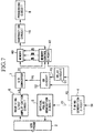
- FIG. 7 is a block diagram showing a circuit configuration for the EOS oscilloscope in accordance with another embodiment of the invention. As compared with the aforementioned circuit configuration of FIG. 1, the circuit configuration of FIG. 7 is made such that the latch circuit 13 is replaced by a memory 40 and a control circuit 41.
- FIG. 8A shows a pulse signal P1 which the timing generation circuit 4 outputs to the optical pulse generation circuit 5.
- FIG. 8B shows a receiving light signal LS which the receiving light amplification circuit 6 outputs.
- FIG. 8C shows a sampling pulse signal PS which the OR circuit 12 outputs to the A/D converter 7.
- FIG. 8D shows data D1 which the A/D converter 7 outputs.
- the above signals and data are identical in timing and waveform (or data values) to those used in the aforementioned EOS oscilloscope of FIG. 1; hence, the description thereof will be omitted.
- FIG. 8E shows an address pulse signal consisting of address output pulses which are created in the memory control circuit 41.
- FIG. 8F shows content of data representing memory addresses AD, each of which is created by the memory control circuit 41 and is then supplied to an address terminal of the memory 40 at a leading-edge timing of the address output pulse.
- FIG. 8G shows a memory read signal MR which the memory control circuit 41 outputs to the memory 40. When the memory read signal MR is output, data are read from an address of the memory 40 designated by the memory address AD and are then supplied to the memory control circuit 41.
- FIG. 8H shows a signal consisting of data load pulses, which are created in the memory control circuit 41. When issuing the data load pulse, the memory control circuit 41 loads the data D1 output from the A/D converter 7.
- FIG. 8I shows a memory write signal MW which is created in the memory control circuit 41.
- the memory control circuit 41 supplies the added data to a data input terminal of the memory 40.
- the added data are written into an address of the memory 40 designated by the memory address AD.
- FIG. 8J shows memory input/output data of the memory 40. As shown in FIG.
- the data D1 output from the A/D converter 7 alternatively designate detection data and noise data
- the memory address AD sequentially designates addresses such as address 1, address 2, ...
- the memory 40 and the memory control circuit 41 cooperate together to perform sequential addition (or accumulation) with respect to the detection data and noise data respectively.
- "MD1" designates previously added data (i.e., added detection data) which are read from address 1 of the memory 40
- "MD2" designates data, which are produced by adding the present detection data (i.e., data D1, see FIG. 8D) to the previously added data read from the address 1 of the memory 40 and which are written into the memory 40.
- MD3 designates previously added data which are read from address 2 of the memory 40
- MD4 designates previously added data (i.e., added noise data) which are read from address 2 of the memory 40
- MD4 designates data, which are produced by adding the present noise data (i.e., data D1, see FIG. 8D) to the previously added data read from the address 2 of the memory and which are written into the memory 40.
- FIG. 9A shows relationships between addresses of the memory 40 and contents of data written into the memory 40
- FIG. 9B shows an EOS waveform which is displayed based on the stored contents of the memory 40.
- first detection data representing a signal magnitude for a leftmost end position of the waveform are written at the address 1 of the memory 1
- first noise data representing a noise magnitude for the leftmost end position of the waveform are written at the address 2 of the memory 1.
- the subtracter 14 subtracts the first noise data "b" from the first detection data "a” to designate magnitude for the waveform of FIG. 9B at its leftmost end position.
- the EOS oscilloscope of FIG. 7 is designed such that the added data (e.g., average data), which are produced with respect to data of each sample point every measurement period, are accumulated in the memory 40. Then, the accumulated data are read from the memory at the prescribed timing, so that the subtraction circuit 14 performs subtraction of noise components.
- the processing circuit 8 works to display measurement results based on outputs of the subtraction circuit 14.
Landscapes
- Physics & Mathematics (AREA)
- General Physics & Mathematics (AREA)
- Tests Of Electronic Circuits (AREA)
- Measurement Of Current Or Voltage (AREA)
Applications Claiming Priority (2)
| Application Number | Priority Date | Filing Date | Title |
|---|---|---|---|
| JP10070872A JPH11271363A (ja) | 1998-03-19 | 1998-03-19 | 電気光学サンプリングオシロスコープ |
| JP7087298 | 1998-03-19 |
Publications (2)
| Publication Number | Publication Date |
|---|---|
| EP0943925A2 true EP0943925A2 (de) | 1999-09-22 |
| EP0943925A3 EP0943925A3 (de) | 2000-05-31 |
Family
ID=13444093
Family Applications (1)
| Application Number | Title | Priority Date | Filing Date |
|---|---|---|---|
| EP99302013A Withdrawn EP0943925A3 (de) | 1998-03-19 | 1999-03-16 | Elektro-optisches Abtast-Oszilloskop |
Country Status (3)
| Country | Link |
|---|---|
| US (1) | US6232765B1 (de) |
| EP (1) | EP0943925A3 (de) |
| JP (1) | JPH11271363A (de) |
Cited By (3)
| Publication number | Priority date | Publication date | Assignee | Title |
|---|---|---|---|---|
| CN104374972A (zh) * | 2014-11-25 | 2015-02-25 | 苏州立瓷电子技术有限公司 | 一种高精度示波器 |
| CN105675985A (zh) * | 2016-01-19 | 2016-06-15 | 中国科学院上海微系统与信息技术研究所 | 一种脉冲波形测试方法 |
| CN113009201A (zh) * | 2021-02-24 | 2021-06-22 | 普源精电科技股份有限公司 | 一种电信号采样装置 |
Families Citing this family (5)
| Publication number | Priority date | Publication date | Assignee | Title |
|---|---|---|---|---|
| US6636056B1 (en) * | 2000-10-20 | 2003-10-21 | Intel Corporation | Apparatus and method for testing integrated circuits |
| CN100439931C (zh) * | 2005-11-29 | 2008-12-03 | 吉林大学 | 可校准电压的电光探测器 |
| KR101679527B1 (ko) | 2013-02-01 | 2016-11-24 | 하마마츠 포토닉스 가부시키가이샤 | 반도체 디바이스 검사 장치 및 반도체 디바이스 검사 방법 |
| CN105675984B (zh) * | 2016-01-19 | 2019-03-29 | 中国科学院上海微系统与信息技术研究所 | 一种脉冲波形测试电路 |
| JP6611387B1 (ja) * | 2018-08-30 | 2019-11-27 | 浜松ホトニクス株式会社 | 半導体試料の検査装置及び検査方法 |
Family Cites Families (20)
| Publication number | Priority date | Publication date | Assignee | Title |
|---|---|---|---|---|
| US3925727A (en) * | 1973-09-28 | 1975-12-09 | Bell Telephone Labor Inc | Optical sampling oscilloscope utilizing organ arrays of optical fibers |
| CH633889A5 (de) * | 1978-11-24 | 1982-12-31 | Bbc Brown Boveri & Cie | Digitalvoltmeter mit elektrooptischer anzeige der wellenform. |
| JPS5693052A (en) * | 1979-12-27 | 1981-07-28 | Iwatsu Electric Co Ltd | Observation system of wave form |
| US4694244A (en) * | 1986-02-21 | 1987-09-15 | Hewlett Packard Company | Apparatus for random repetitive sampling |
| HU205668B (en) * | 1989-02-22 | 1992-05-28 | Miklos Daka | Method and circuit arrangement for high-precision transient examination of high-frequency active and passive circuits |
| JP2607798B2 (ja) | 1991-03-18 | 1997-05-07 | 日本電信電話株式会社 | 集積回路の電圧信号測定方法および測定装置 |
| JP2542754B2 (ja) | 1991-08-05 | 1996-10-09 | 日本電信電話株式会社 | 集積回路の電界測定用プロ―ブ位置決め方法および位置決め装置 |
| JPH0547883A (ja) | 1991-08-12 | 1993-02-26 | Nippon Telegr & Teleph Corp <Ntt> | 集積回路の回路試験装置および回路試験方法 |
| JPH0580083A (ja) | 1991-09-20 | 1993-03-30 | Nippon Telegr & Teleph Corp <Ntt> | 集積回路の試験方法および装置 |
| JP3187505B2 (ja) | 1992-03-02 | 2001-07-11 | 日本電信電話株式会社 | 集積回路の電界測定装置 |
| JP3139644B2 (ja) | 1992-09-11 | 2001-03-05 | 日本電信電話株式会社 | 集積回路の電圧信号測定装置 |
| JP3165873B2 (ja) | 1993-08-06 | 2001-05-14 | 日本電信電話株式会社 | 電気信号測定方法および装置 |
| JPH0755891A (ja) | 1993-08-09 | 1995-03-03 | Nippon Telegr & Teleph Corp <Ntt> | 集積回路の試験方法および試験装置 |
| JPH0843499A (ja) | 1994-08-03 | 1996-02-16 | Nippon Telegr & Teleph Corp <Ntt> | ティップ型回路試験用電界センサおよびその電界検出方法 |
| JP3489701B2 (ja) | 1994-08-04 | 2004-01-26 | 日本電信電話株式会社 | 電気信号測定装置 |
| JPH08152361A (ja) | 1994-11-29 | 1996-06-11 | Nippon Telegr & Teleph Corp <Ntt> | 光信号波形の測定装置 |
| JPH08160110A (ja) | 1994-12-06 | 1996-06-21 | Nippon Telegr & Teleph Corp <Ntt> | 電気信号測定装置 |
| JP3326317B2 (ja) | 1995-12-05 | 2002-09-24 | 横河電機株式会社 | 電圧測定装置 |
| JP3334743B2 (ja) | 1996-01-19 | 2002-10-15 | 日本電信電話株式会社 | 電気信号測定装置 |
| JPH09211035A (ja) | 1996-01-30 | 1997-08-15 | Nippon Telegr & Teleph Corp <Ntt> | 電界測定装置 |
-
1998
- 1998-03-19 JP JP10070872A patent/JPH11271363A/ja active Pending
-
1999
- 1999-03-12 US US09/268,136 patent/US6232765B1/en not_active Expired - Fee Related
- 1999-03-16 EP EP99302013A patent/EP0943925A3/de not_active Withdrawn
Cited By (6)
| Publication number | Priority date | Publication date | Assignee | Title |
|---|---|---|---|---|
| CN104374972A (zh) * | 2014-11-25 | 2015-02-25 | 苏州立瓷电子技术有限公司 | 一种高精度示波器 |
| CN105675985A (zh) * | 2016-01-19 | 2016-06-15 | 中国科学院上海微系统与信息技术研究所 | 一种脉冲波形测试方法 |
| CN105675985B (zh) * | 2016-01-19 | 2019-03-29 | 中国科学院上海微系统与信息技术研究所 | 一种脉冲波形测试方法 |
| CN113009201A (zh) * | 2021-02-24 | 2021-06-22 | 普源精电科技股份有限公司 | 一种电信号采样装置 |
| CN113009201B (zh) * | 2021-02-24 | 2022-08-23 | 普源精电科技股份有限公司 | 一种电信号采样装置 |
| US12480977B2 (en) | 2021-02-24 | 2025-11-25 | Rigol Technologies Co., Ltd. | Electrical signal sampling device |
Also Published As
| Publication number | Publication date |
|---|---|
| EP0943925A3 (de) | 2000-05-31 |
| US6232765B1 (en) | 2001-05-15 |
| JPH11271363A (ja) | 1999-10-08 |
Similar Documents
| Publication | Publication Date | Title |
|---|---|---|
| US8290032B2 (en) | Distortion identification apparatus, test system, recording medium and distortion identification method | |
| US8358682B2 (en) | Signal processing apparatus, test system, distortion detecting apparatus, signal compensation apparatus, analytic signal generating apparatus, recording medium and analytic signal generating method | |
| JPH1144710A (ja) | 方形波試験信号を使用するオシロスコープの自動校正 | |
| US6232765B1 (en) | Electro-optical oscilloscope with improved sampling | |
| US7184908B2 (en) | Calibration method of time measurement apparatus | |
| US7890074B2 (en) | Data acquisition system | |
| JP2654724B2 (ja) | 光受信器の自動マスキング装置及び光受信器の過渡応答歪補償方法 | |
| US11143679B2 (en) | Method and apparatus for processing a measurement signal | |
| US6998834B2 (en) | Real-time time drift adjustment for a TDR step stimulus | |
| GB2213335A (en) | Calibration of time measurement apparatus | |
| JP4156941B2 (ja) | 複数サンプリングデジタイザのチャンネル間スキュー補正装置及び補正方法 | |
| JP3311464B2 (ja) | 信号測定装置 | |
| JPH11108959A (ja) | 電気光学サンプリングオシロスコープ | |
| JP3323121B2 (ja) | 半導体装置の測定方法及び測定装置 | |
| EP0921402A2 (de) | Elektro-optisches Abtast-oszilloskop | |
| JP3839705B2 (ja) | 標本化方法および装置、ならびに、推測方法および装置 | |
| JPH11352156A (ja) | 電気光学サンプリングオシロスコープ | |
| US6087838A (en) | Signal processing circuit for electro-optic probe | |
| JP3406491B2 (ja) | 電気光学サンプリングオシロスコープ | |
| CN120468922B (zh) | 一种基于腔式探头的束团间信号混叠校准方法 | |
| JPH0712852A (ja) | 波形生成機能付き波形測定装置 | |
| JP3244929B2 (ja) | サンプリング装置 | |
| JPH04190163A (ja) | ノイズ除去機能を有するオシロスコープ | |
| CN1281988A (zh) | 一种信号采样方法及信号检测显示系统 | |
| JP3373742B2 (ja) | Ac/dc変換装置及び方法 |
Legal Events
| Date | Code | Title | Description |
|---|---|---|---|
| PUAI | Public reference made under article 153(3) epc to a published international application that has entered the european phase |
Free format text: ORIGINAL CODE: 0009012 |
|
| AK | Designated contracting states |
Kind code of ref document: A2 Designated state(s): DE FR GB |
|
| AX | Request for extension of the european patent |
Free format text: AL;LT;LV;MK;RO;SI |
|
| RIN1 | Information on inventor provided before grant (corrected) |
Inventor name: YAMADA, JUNZO Inventor name: NAGATSUMA, TADAO, Inventor name: SHINAGAWA, MITSURU, Inventor name: ENDOU, YOSHIO Inventor name: BANJOU, NOBUKAZU Inventor name: KIKUCHI, JUN Inventor name: YANAGISAWA, YOSHIKI Inventor name: TAKEUCHI, NOBUAKI |
|
| PUAL | Search report despatched |
Free format text: ORIGINAL CODE: 0009013 |
|
| AK | Designated contracting states |
Kind code of ref document: A3 Designated state(s): AT BE CH CY DE DK ES FI FR GB GR IE IT LI LU MC NL PT SE |
|
| AX | Request for extension of the european patent |
Free format text: AL;LT;LV;MK;RO;SI |
|
| RIC1 | Information provided on ipc code assigned before grant |
Free format text: 7G 01R 13/34 A, 7G 01R 19/25 B |
|
| 17P | Request for examination filed |
Effective date: 20000912 |
|
| AKX | Designation fees paid |
Free format text: DE FR GB |
|
| RAP1 | Party data changed (applicant data changed or rights of an application transferred) |
Owner name: NIPPON TELEGRAPH ANDTELEPHONE CORPORATION Owner name: YOKOGAWA ELECTRIC CORPORATION |
|
| STAA | Information on the status of an ep patent application or granted ep patent |
Free format text: STATUS: THE APPLICATION IS DEEMED TO BE WITHDRAWN |
|
| 18D | Application deemed to be withdrawn |
Effective date: 20060223 |