EP0933808B1 - Verfahren und Vorrichtung zur Harzversiegelung einer Halbleitervorrichtung - Google Patents
Verfahren und Vorrichtung zur Harzversiegelung einer Halbleitervorrichtung Download PDFInfo
- Publication number
- EP0933808B1 EP0933808B1 EP99101128A EP99101128A EP0933808B1 EP 0933808 B1 EP0933808 B1 EP 0933808B1 EP 99101128 A EP99101128 A EP 99101128A EP 99101128 A EP99101128 A EP 99101128A EP 0933808 B1 EP0933808 B1 EP 0933808B1
- Authority
- EP
- European Patent Office
- Prior art keywords
- resin
- sealing
- release film
- semiconductor chip
- underfilled
- Prior art date
- Legal status (The legal status is an assumption and is not a legal conclusion. Google has not performed a legal analysis and makes no representation as to the accuracy of the status listed.)
- Expired - Lifetime
Links
Images



Classifications
-
- H—ELECTRICITY
- H10—SEMICONDUCTOR DEVICES; ELECTRIC SOLID-STATE DEVICES NOT OTHERWISE PROVIDED FOR
- H10W—GENERIC PACKAGES, INTERCONNECTIONS, CONNECTORS OR OTHER CONSTRUCTIONAL DETAILS OF DEVICES COVERED BY CLASS H10
- H10W74/00—Encapsulations, e.g. protective coatings
- H10W74/01—Manufacture or treatment
- H10W74/016—Manufacture or treatment using moulds
- H10W74/017—Auxiliary layers for moulds, e.g. release layers or layers preventing residue
-
- B—PERFORMING OPERATIONS; TRANSPORTING
- B29—WORKING OF PLASTICS; WORKING OF SUBSTANCES IN A PLASTIC STATE IN GENERAL
- B29C—SHAPING OR JOINING OF PLASTICS; SHAPING OF MATERIAL IN A PLASTIC STATE, NOT OTHERWISE PROVIDED FOR; AFTER-TREATMENT OF THE SHAPED PRODUCTS, e.g. REPAIRING
- B29C45/00—Injection moulding, i.e. forcing the required volume of moulding material through a nozzle into a closed mould; Apparatus therefor
- B29C45/14—Injection moulding, i.e. forcing the required volume of moulding material through a nozzle into a closed mould; Apparatus therefor incorporating preformed parts or layers, e.g. injection moulding around inserts or for coating articles
- B29C45/14639—Injection moulding, i.e. forcing the required volume of moulding material through a nozzle into a closed mould; Apparatus therefor incorporating preformed parts or layers, e.g. injection moulding around inserts or for coating articles for obtaining an insulating effect, e.g. for electrical components
- B29C45/14655—Injection moulding, i.e. forcing the required volume of moulding material through a nozzle into a closed mould; Apparatus therefor incorporating preformed parts or layers, e.g. injection moulding around inserts or for coating articles for obtaining an insulating effect, e.g. for electrical components connected to or mounted on a carrier, e.g. lead frame
-
- H—ELECTRICITY
- H10—SEMICONDUCTOR DEVICES; ELECTRIC SOLID-STATE DEVICES NOT OTHERWISE PROVIDED FOR
- H10P—GENERIC PROCESSES OR APPARATUS FOR THE MANUFACTURE OR TREATMENT OF DEVICES COVERED BY CLASS H10
- H10P72/00—Handling or holding of wafers, substrates or devices during manufacture or treatment thereof
- H10P72/04—Apparatus for manufacture or treatment
- H10P72/0441—Apparatus for sealing, encapsulating, glassing, decapsulating or the like
-
- H—ELECTRICITY
- H10—SEMICONDUCTOR DEVICES; ELECTRIC SOLID-STATE DEVICES NOT OTHERWISE PROVIDED FOR
- H10W—GENERIC PACKAGES, INTERCONNECTIONS, CONNECTORS OR OTHER CONSTRUCTIONAL DETAILS OF DEVICES COVERED BY CLASS H10
- H10W70/00—Package substrates; Interposers; Redistribution layers [RDL]
- H10W70/60—Insulating or insulated package substrates; Interposers; Redistribution layers
-
- H—ELECTRICITY
- H10—SEMICONDUCTOR DEVICES; ELECTRIC SOLID-STATE DEVICES NOT OTHERWISE PROVIDED FOR
- H10W—GENERIC PACKAGES, INTERCONNECTIONS, CONNECTORS OR OTHER CONSTRUCTIONAL DETAILS OF DEVICES COVERED BY CLASS H10
- H10W74/00—Encapsulations, e.g. protective coatings
- H10W74/01—Manufacture or treatment
- H10W74/012—Manufacture or treatment of encapsulations on active surfaces of flip-chip devices, e.g. forming underfills
-
- H—ELECTRICITY
- H10—SEMICONDUCTOR DEVICES; ELECTRIC SOLID-STATE DEVICES NOT OTHERWISE PROVIDED FOR
- H10W—GENERIC PACKAGES, INTERCONNECTIONS, CONNECTORS OR OTHER CONSTRUCTIONAL DETAILS OF DEVICES COVERED BY CLASS H10
- H10W74/00—Encapsulations, e.g. protective coatings
- H10W74/10—Encapsulations, e.g. protective coatings characterised by their shape or disposition
- H10W74/15—Encapsulations, e.g. protective coatings characterised by their shape or disposition on active surfaces of flip-chip devices, e.g. underfills
-
- B—PERFORMING OPERATIONS; TRANSPORTING
- B29—WORKING OF PLASTICS; WORKING OF SUBSTANCES IN A PLASTIC STATE IN GENERAL
- B29C—SHAPING OR JOINING OF PLASTICS; SHAPING OF MATERIAL IN A PLASTIC STATE, NOT OTHERWISE PROVIDED FOR; AFTER-TREATMENT OF THE SHAPED PRODUCTS, e.g. REPAIRING
- B29C43/00—Compression moulding, i.e. applying external pressure to flow the moulding material; Apparatus therefor
- B29C43/32—Component parts, details or accessories; Auxiliary operations
- B29C43/58—Measuring, controlling or regulating
- B29C2043/5875—Measuring, controlling or regulating the material feed to the moulds or mould parts, e.g. controlling feed flow, velocity, weight, doses
-
- B—PERFORMING OPERATIONS; TRANSPORTING
- B29—WORKING OF PLASTICS; WORKING OF SUBSTANCES IN A PLASTIC STATE IN GENERAL
- B29C—SHAPING OR JOINING OF PLASTICS; SHAPING OF MATERIAL IN A PLASTIC STATE, NOT OTHERWISE PROVIDED FOR; AFTER-TREATMENT OF THE SHAPED PRODUCTS, e.g. REPAIRING
- B29C45/00—Injection moulding, i.e. forcing the required volume of moulding material through a nozzle into a closed mould; Apparatus therefor
- B29C45/14—Injection moulding, i.e. forcing the required volume of moulding material through a nozzle into a closed mould; Apparatus therefor incorporating preformed parts or layers, e.g. injection moulding around inserts or for coating articles
- B29C45/14639—Injection moulding, i.e. forcing the required volume of moulding material through a nozzle into a closed mould; Apparatus therefor incorporating preformed parts or layers, e.g. injection moulding around inserts or for coating articles for obtaining an insulating effect, e.g. for electrical components
- B29C45/14655—Injection moulding, i.e. forcing the required volume of moulding material through a nozzle into a closed mould; Apparatus therefor incorporating preformed parts or layers, e.g. injection moulding around inserts or for coating articles for obtaining an insulating effect, e.g. for electrical components connected to or mounted on a carrier, e.g. lead frame
- B29C2045/14663—Injection moulding, i.e. forcing the required volume of moulding material through a nozzle into a closed mould; Apparatus therefor incorporating preformed parts or layers, e.g. injection moulding around inserts or for coating articles for obtaining an insulating effect, e.g. for electrical components connected to or mounted on a carrier, e.g. lead frame the mould cavity walls being lined with a film, e.g. release film
-
- B—PERFORMING OPERATIONS; TRANSPORTING
- B29—WORKING OF PLASTICS; WORKING OF SUBSTANCES IN A PLASTIC STATE IN GENERAL
- B29C—SHAPING OR JOINING OF PLASTICS; SHAPING OF MATERIAL IN A PLASTIC STATE, NOT OTHERWISE PROVIDED FOR; AFTER-TREATMENT OF THE SHAPED PRODUCTS, e.g. REPAIRING
- B29C2791/00—Shaping characteristics in general
- B29C2791/004—Shaping under special conditions
- B29C2791/008—Using vibrations during moulding
-
- H—ELECTRICITY
- H10—SEMICONDUCTOR DEVICES; ELECTRIC SOLID-STATE DEVICES NOT OTHERWISE PROVIDED FOR
- H10W—GENERIC PACKAGES, INTERCONNECTIONS, CONNECTORS OR OTHER CONSTRUCTIONAL DETAILS OF DEVICES COVERED BY CLASS H10
- H10W72/00—Interconnections or connectors in packages
- H10W72/071—Connecting or disconnecting
- H10W72/0711—Apparatus therefor
- H10W72/07141—Means for applying energy, e.g. ovens or lasers
-
- H—ELECTRICITY
- H10—SEMICONDUCTOR DEVICES; ELECTRIC SOLID-STATE DEVICES NOT OTHERWISE PROVIDED FOR
- H10W—GENERIC PACKAGES, INTERCONNECTIONS, CONNECTORS OR OTHER CONSTRUCTIONAL DETAILS OF DEVICES COVERED BY CLASS H10
- H10W72/00—Interconnections or connectors in packages
- H10W72/071—Connecting or disconnecting
- H10W72/072—Connecting or disconnecting of bump connectors
-
- H—ELECTRICITY
- H10—SEMICONDUCTOR DEVICES; ELECTRIC SOLID-STATE DEVICES NOT OTHERWISE PROVIDED FOR
- H10W—GENERIC PACKAGES, INTERCONNECTIONS, CONNECTORS OR OTHER CONSTRUCTIONAL DETAILS OF DEVICES COVERED BY CLASS H10
- H10W72/00—Interconnections or connectors in packages
- H10W72/071—Connecting or disconnecting
- H10W72/073—Connecting or disconnecting of die-attach connectors
-
- H—ELECTRICITY
- H10—SEMICONDUCTOR DEVICES; ELECTRIC SOLID-STATE DEVICES NOT OTHERWISE PROVIDED FOR
- H10W—GENERIC PACKAGES, INTERCONNECTIONS, CONNECTORS OR OTHER CONSTRUCTIONAL DETAILS OF DEVICES COVERED BY CLASS H10
- H10W72/00—Interconnections or connectors in packages
- H10W72/851—Dispositions of multiple connectors or interconnections
- H10W72/853—On the same surface
- H10W72/856—Bump connectors and die-attach connectors
-
- H—ELECTRICITY
- H10—SEMICONDUCTOR DEVICES; ELECTRIC SOLID-STATE DEVICES NOT OTHERWISE PROVIDED FOR
- H10W—GENERIC PACKAGES, INTERCONNECTIONS, CONNECTORS OR OTHER CONSTRUCTIONAL DETAILS OF DEVICES COVERED BY CLASS H10
- H10W72/00—Interconnections or connectors in packages
- H10W72/90—Bond pads, in general
-
- H—ELECTRICITY
- H10—SEMICONDUCTOR DEVICES; ELECTRIC SOLID-STATE DEVICES NOT OTHERWISE PROVIDED FOR
- H10W—GENERIC PACKAGES, INTERCONNECTIONS, CONNECTORS OR OTHER CONSTRUCTIONAL DETAILS OF DEVICES COVERED BY CLASS H10
- H10W72/00—Interconnections or connectors in packages
- H10W72/90—Bond pads, in general
- H10W72/941—Dispositions of bond pads
- H10W72/9415—Dispositions of bond pads relative to the surface, e.g. recessed, protruding
-
- H—ELECTRICITY
- H10—SEMICONDUCTOR DEVICES; ELECTRIC SOLID-STATE DEVICES NOT OTHERWISE PROVIDED FOR
- H10W—GENERIC PACKAGES, INTERCONNECTIONS, CONNECTORS OR OTHER CONSTRUCTIONAL DETAILS OF DEVICES COVERED BY CLASS H10
- H10W74/00—Encapsulations, e.g. protective coatings
-
- H—ELECTRICITY
- H10—SEMICONDUCTOR DEVICES; ELECTRIC SOLID-STATE DEVICES NOT OTHERWISE PROVIDED FOR
- H10W—GENERIC PACKAGES, INTERCONNECTIONS, CONNECTORS OR OTHER CONSTRUCTIONAL DETAILS OF DEVICES COVERED BY CLASS H10
- H10W90/00—Package configurations
- H10W90/701—Package configurations characterised by the relative positions of pads or connectors relative to package parts
- H10W90/721—Package configurations characterised by the relative positions of pads or connectors relative to package parts of bump connectors
- H10W90/724—Package configurations characterised by the relative positions of pads or connectors relative to package parts of bump connectors between a chip and a stacked insulating package substrate, interposer or RDL
Definitions
- the present invention relates to a resin sealing method and apparatus for a semiconductor device. More particularly, the invention relates to a resin sealing method and apparatus which are well adaptable for the resin sealing of a semiconductor device having an underfill structure, e.g., a semiconductor device including a flip-chip connected semiconductor chip.
- a semiconductor device having a semiconductor chip mounted by a flip chip method is shown in Fig. 6 .
- a semiconductor chip 12 is flip-chip connected onto a substrate 10, and then a joining portion between the semiconductor chip 12 and the substrate 10 is filled with sealing resin 14, to thereby seal the joining portion by resin.
- the sealing resin 14 functions to protect the joining portion between the semiconductor chip 12 and the substrate 10 and to relieve a thermal stress caused by the thermal coefficient difference of expansion between the substrate 10 and the semiconductor chip 12.
- FIG. 7 A known method of filling the joining portion with resin 14, generally used, is shown in Fig. 7 .
- the substrate 10 is slantly supported, and in this state, sealing resin 14 is allowed to flow into the joining portion between the substrate 10 and the semiconductor chip 12.
- a number of solder bumps 16 are studded on the joining portion between the substrate 10 and the semiconductor chip 12.
- the sealing resin 14 flows through gaps among those bumps 16.
- the substrate 10 is slanted, and the sealing resin 14 flows onto the slanted substrate 10 while expelling air from the joining portion.
- the sealing resin 14 When the sealing resin 14 is allowed to merely flow into the joining portion of the flip-chip connected semiconductor chip 12 to fill out there, the sealing resin 14 imperfectly fills the joining portion between the semiconductor chip 12, and sometimes the substrate 10 and air bubbles are left in the gap portion.
- the width of the joining portion (between the semiconductor chip 12 and the substrate 10) is about 0.1mm, and recently it is reduced from 0.1mm to 0.02 mm to 0.03mm, extremely narrow.
- a number of solder bumps 16 are studded in the joining portion, and those bumps restrict the flow of the sealing resin 14.
- the filler-contained resin is used, the resin flow is further impeded. Therefore, the method of merely flowing the sealing resin 14 into the underfilled portion cannot achieve the reliable sealing.
- a resin hardening time in the potting process is longer than in the transfer molding process. Therefore, also in the work efficiency, the method by merely flowing the sealing resin 14 into the underfilled portion is not preferable.
- the solder bumps are minutely different in height and the semiconductor chips are also minutely different in thickness with the pieces to be molded. Therefore, when the transfer molding is used for sealing flip-chip connected semiconductor chip by resin, the following disadvantages are present: 1) a thin layer of resin will be formed on the outer surface of the semiconductor chip; and 2) the resin excessively presses the molded piece to possibly break the molded piece. Further, the resin material including extremely small silica particles or not including the same must be used since the gaps in the underfilled portion are extremely small. Such a resin material is easy to enter the gaps. Therefore, if the clamping of the molded piece is not properly, the resin will enter the gaps to form resin flash. The same disadvantageous phenomenon occurs also when the semiconductor chip is minutely displaced (when viewed in plan) on the substrate. For this reason, it is almost impossible to resin seal the underfilled portion resulting from the flip-chip connection by the conventional transfer molding process.
- EP-A-0730937 A1 discloses a resin molding machine with a release film in which the release film is fixed to the inner surfaces of the mold cavities.
- the release film serves to facilitate the separation of the molded piece from the inner cavities only. It is, however, not used to delimit the perimeter of the underfilled portion in that it is pressed against side surfaces of the semiconductor chip when the mold is closed.
- WO97/27624 discloses a method and device to encapsulate integrated circuits by pressurized underfill encapsulation.
- the device uses a specific mold to surround a chip of the IC.
- the mold is dimensioned such that the side faces of the chip are free so that the molding resin can flow and adhere to the side faces.
- JP 09 312308 A discloses to apply an ultrasonic vibration to resin flowing in a die to remove voids or poor charge.
- an object of the present invention is to provide a resin sealing method for sealing a semiconductor device with resin which is improved such that a transfer molding process is used for manufacturing a semiconductor device having an underfill structure, e.g. a semicondductor device including a flip-chip connected semiconductor chip, and the use of the transfer molding process provides a reliable underfilling free from air bubbles and produces a reliable semiconductor device, and an efficient underfilling process is provided.
- a transfer molding process is used for manufacturing a semiconductor device having an underfill structure, e.g. a semicondductor device including a flip-chip connected semiconductor chip
- Another object of the invention is to provide a resin sealing apparatus achieving the same improvements as by the resin sealing method.
- the present invention provides a resin sealing method as defined in claim 1 and a resin sealing apparatus as defined in claim 5.
- the resin material may take the form of a cylindrical resin tablet, and the resin tablet is placed which being laid down on the clamping surface of the mold, whereby the resin filling is performed.
- the film when the underfilled portion is closed by the release film, the film is preferably pressed against the side face of the semiconductor chip, through an elastic member elastically deformable when it receives a clamping force for clamping the molded piece.
- a pulsative motion is preferably applied to the sealing resin.
- an elastic member is preferably provided on side surface of the cavity recess, when the molded piece is clamped, the elastic member is elastically deformed by a clamping force produced to press the release film against the side face of the semiconductor chip.
- the resin sealing apparatus further comprises preferably pulsating means for pulsating the sealing resin when the' pressurized sealing resin is fed to the underfilled portion.
- the resin sealing apparatus fills, with sealing resin, a gap portion (underfilled portion) of the jointing portion between the substrate 10 and the semiconductor chip 12 in a piece 40 to be molded (moulded piece), which is carried on a carrier substrate 10 by the flip chip connection, by a transfer molding process using a release film ( Fig. 1 ).
- the "release film” means a film having a heat resistance high enough to endure the heating temperature of a semiconductor mold and such a releasability as to allow the resin to release from the mold, and such a flexibility as to be expandable and deformable in conformity with a configuration of a mold face having a cavity or impression.
- a method in which in the process of resin sealing, the mold face is covered with a release film is called a "resin sealing method using a release film”.
- the release film are ETFE, PTFE, PET, FEP, polyvinylidene chloride, and fluorine-contained glass cloth, and a thickness of the release film is 25 ⁇ m or less.
- the mold face is covered with the release film. Because of this, there is no chance that the resin directly contacts with the mold face. Therefore, a molded piece is easily released from the mold; the mold is simplified; and a resin material most suitable for a product or piece to be molded may be selected while having no regard for the releasability of the molded piece.
- Fig. 1 is a sectional view showing a semiconductor mold in a resin sealing apparatus for sealing a molded piece 40 by resin.
- the left half portion of the illustration with respect to the center line CL shows a state of the molded piece 40 being clamped with the top half 26 and the bottom half 28 of the mold.
- the right half portion with respect to the center line CL shows a state that a gap portion (underfilled portion) of the joining portion of the semiconductor chip 12 and the carrier substrate 10 is filled with sealing resin.
- Molded pieces 40 are respectively disposed on both sides of a pot 42 of the illustrated mold. Sealing resin which is molten within the pot 42 is transferred, under pressure, to the underfilled portion of each molded piece 40 by a plunger 44.
- Reference numeral 46 is a set recess used for setting the molded piece 40 at a predetermined location of the bottom half 28 of the mold.
- Numeral 48 is a molding cull, and numeral 50 is a mold runner communicating with the pot 42.
- Numeral 52 is a heater for heating the bottom half 28, and numeral 54 is an air absorbing hole for attracting a release film 20 that is set on the bottom half 28 onto the parting face of the bottom half 28, by air absorption.
- the top half 26 of the mold includes a cull insert 60 located facing the pot 42, and cavity inserts 62 located so as to be able to clamp the molded piece 40.
- a cavity recess 62a for receiving a semiconductor chip 12 carried on the substrate 10 is formed in the parting face of the cavity insert 62.
- the cavity recess 62a tightly presses the side faces of the semiconductor chip 12 in such a way that the release film 20 is placed between the cavity recess and the side faces of the chip.
- a gap which will serve as an air passage 64, is formed connecting from the inner wall of the set hole of the top half 26 to the side surface of the cavity insert 62.
- the air passage 64 attracts, by air' absorption, a release film 20 that is set on the parting face of the top half 26, onto that parting face.
- Numeral 66 is an air passage which is provided in the side surface of the cull insert 60 in order to attract the release film 20 to the cull portion by air attraction.
- Numeral 62b is an absorption hole for attracting the release film 20 onto the inner surface of the cavity recess 62a by air absorption.
- the parting face of the top half 26 is substantially entirely covered with the release film 20, and the inner surface of the cavity recess 62a of the cavity insert 62 is also covered with the release film 20. Therefore, the dimension of the cavity recess 62a of the cavity insert 62 is so selected that it can receive a semiconductor chip 12 in a state that the cavity recess 62a is covered with the release film 20.
- Numeral 68 indicates ultrasonic vibrators installed in the top half 26 of the mold. Each ultrasonic vibrator 68 is disposed in alignment with the position of a gate 70. The ultrasonic vibrator 68 vibrates resin passing through the gate 70 to reliably fill the underfilled portion with resin. In case where the sealing resin contains filler, the operation of the ultrasonic vibrator 68 is effective for filling the underfilled portion with the resin. No resin enters the ultrasonic vibrator 68 Because of presence of the release film 20, and hence it is stable in its operation.
- Numeral 74 is a heater provided in the base 72 of the top half 26.
- molded pieces 40 are put in the set recess 46 of the bottom half 28.
- a release film 20 is supplied to the parting face between the top half 26 and the bottom half 28 by use of a film supply mechanism.
- the film In supplying a release film 20 to the mold, the film is somewhat lifted above the parting face of the mold; moved to a predetermined position within the mold; and air is sucked through the air absorbing hole 54 and the air passages 64 and 66, those connecting to the film supply mechanism, so that the release film 20 is attractively supported on the parting face.
- the release film 20 to be supplied to the bottom half 28 has a width large enough to range from the pot 42 to the gate-side ends of the molded pieces 40, placed on both sides of the pot.
- the molded pieces 40 are set to the bottom half 28 of the mold, and then the release film 20 is set to the same.
- the opening portion of the pot 42 is closed by the release film 20, and further, a region up to the gate-side ends of the substrates 10 of the molded pieces 40 are covered with the release film 20.
- a resin tablet 80 for underfilling is supplied to the pot 42 of the bottom half 28, and then the molded pieces 40 are clamped with the top half 26 and the bottom half 28.
- the opening portion of the pot 42 is closed with the release film 20; however, it is inserted into the pot 42 when the molded pieces 40 are clamped.
- the release film 20 is easily put into the pot 42 since the release film 20 is satisfactorily expandable and flexible. It is preferable that the resin tablet 80 is horizontally placed since an easy expansion of the release film 20 is allowed.
- the plunger 44 is driven to push up the molten resin, the molten resin flows through the mold runners 50 and the gates 70, and reaches the underfilled portion and fills the underfilled portion.
- the sealing resin to be supplied to the pot 42 takes the form of a tablet. If required, it may take form of granule, powder, or liquid resin, or lapping resin.
- the "lapping resin”, formed with a lapping film, consists of a container containing a predetermined amount of resin, shaped so as to be received by the pot 42, and extended portions extended from both sides of the container. Two sheets of lapping films are laminated to sealingly form the extended portions. When resin pressure is applied to the extended portions, those laminated portions are separated from each other, and the resin flows outside through the space between the separated lapping films, from the container.
- the underfilling is effected which is comparable with that in the above-mentioned embodiment, without setting the release film 20 to the bottom half 28.
- Liquid resin may be used for the resin to be contained in the container of the lapping resin.
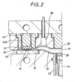
- Fig. 2 is an explanatory diagram showing a state that the underfilled portion of a molded piece 40 is filled with sealing resin.
- a pressure by the sealing resin 14 transferred under pressure from the pot 42 presses the release film 20 against the inner wall of the mold. Therefore, in the process of filling the underfilled portion with the sealing resin 14, there is no chance that the sealing resin 14 contacts with the inner wall of the mold.
- the end of the gate 70 is connected to the opening end of the gap between the semiconductor chip 12 and the substrate 10. With this connection, the sealing resin 14 is fed to the underfilled portion, from the gate 70.
- the sealing resin 14 is injected through the gate 70 into the underfilled portion, to effect the fill-out of this portion.
- the resin sealing method of the embodiment clamps the molded piece 40 by the mold, and injects the sealing resin 14 into the underfilled portion by pressurizing the sealing resin 14 by the plunger 44, whereby the fill-out of the underfilled portion by the sealing resin is effected.
- the resin sealing method can more reliably seal the underfilled portion than the conventional resin sealing method in which the sealing resin is allowed to merely flow into the underfilled portion.
- the resin sealing method using the pressurized resin for the fill-out of the underfilled portion can realize a reliable resin sealing.
- the molded piece 40 is clamped in a state that the release film 20 is placed between the molded piece 40 and the parting face of the mold. Therefore, the release film 20 protects the outer surface of the semiconductor chip 12, and there is no chance that the clamping force will break the semiconductor chip 12.
- the clamping of the molded piece with the insertion of the release film 20 between the molded piece and the mold enhances the sealing performance, and eliminates the formation of the flash of the underfilling material on the outer surface of the semiconductor chip 12.
- the mold piece clamping with the release film insertion enhances the sealing of the underfilled portion. As a result, there is no chance that the flash of the underfilling material is formed on the substrate 10 carrying the semiconductor chip 12.
- the gate 70 may be connected to the underfilled portion by 1) connecting the gate to a proper position on the side of the gate 70 to which the gate is to be connected, or 2) connecting the gate to the entire side (gate end) of the gate 70 to which the gate is to be connected.
- the second gate connecting method is advantageous in that an efficient injection of the sealing resin into the underfilled portion is possible.
- the mold is opened, and the molded pieces sealed with resin are taken out of the mold.
- the underfilling process under the condition of the insertion of the release film 20 provides an easy releasing of the molded pieces. Therefore, only the molded pieces may be taken out by releasing the release film 20 from the molded pieces.
- the mold is opened, molded pieces 40 are set on the bottom half 28 of the mold, and a new release film 20 is set on the parting face between the top half 26 and the bottom half 28. In this way, the molded pieces are successively sealed with resin by the transfer molding process using the release film.
- the resin sealing apparatus described above fills the underfilled portion of the molded piece 40 with resin while applying the resin pressure to the underfilled portion. Therefore, the cavity recess 62a is formed in the parting face of the cavity insert 62 of the top half 26 of the mold, and the underfilled portion is closed by surrounding the underfilled portion by the release film 20.
- Fig. 3 is an explanatory diagram showing another structure of the semiconductor mold for surrounding and closing the underfilled portion of the semiconductor chip by the release film 20.
- the left half with respect to the center line CL shows a state that a molded piece 40 is not yet clamped, while the right half shows a state that the molded piece 40 is clamped.
- a cavity insert 62 for receiving a semiconductor chip 12 is provided.
- This structure is different from the previous structure in that an elastic member 90 of silicone rubber, for example, is additionally located at a portion of the structure where it contacts with the side face of the semiconductor chip 12.
- the elastic member 90 functions as follows: when the molded piece 40 is clamped with the top and bottom halves of the semiconductor mold, the resultant clamping force presses the elastic member 90 inwardly, and in turn the pressed elastic member presses the release film 20 against the side face of the semiconductor chip 12 and further against the upper surface of the substrate 10.
- the right half with respect to the center line CL in Fig. 3 shows a state where the perimeter of the underfilled portion of the molded piece is closed with the release film 20 with the aid of the elastic member 90.
- the molded piece of which the underfilled portion includes extremely small gaps is sealed with sealing resin, it is essential to reliably seal the underfilled portion.
- Such a reliable sealing can be achieved by use of the elastic member 90.
- the Fig. 3 structure additionally uses an air passage 92 formed at a location between the inner surface of the elastic member 90 and the side surface of the cavity insert 62.
- the air passage 92 functions such that when the molded piece 40 is clamped, air pressure is applied to the elastic member 90 through the air passage 92, to thereby reinforce the pressing force by the elastic member 90 and hence to more reliably close the underfilled portion.
- Fig. 4 is an explanatory diagram showing another structure of the semiconductor mold for surrounding and closing the underfilled portion of the semiconductor chip by the release film with the aid of the elastic member 90.
- the left half with respect to the center line CL shows a state that a molded piece 40 is half opened, while the right half shows a state that the molded piece 40 is clamped.
- the cavity recess 62a of the cavity insert 62 includes a side structure formed with a metal pressure member 94 and an elastic member 90 of, for example, silicone rubber.
- the metal pressure member 94 concentrates a pressing force onto in particular the side face of the underfilled portion.
- the elastic member 90 augmentatively assists the holding of the side of the underfilled portion by the metal pressure member 94, and presses the release film 20 onto the upper surface of the substrate 10.
- the Fig. 4 structure also advantageously operates when the molded piece of which the underfilled portion includes extremely small gaps is sealed with sealing resin: it ensures a reliable fill-out of the underfilled portion by the resin, and provides a reliable resin sealing of the molded piece or semiconductor device. Also in this structure, with application of air pressure through the air passage 92, the release film 20 is reliably pressed against the side face of the semiconductor chip 12, thereby enhancing the closing of the underfilled portion.
- a block is mechanically moved by a drive means, e.g., a cylinder, to close the perimeter of the underfilled portion
- air is fed through the absorption hole 62b to close the perimeter of the underfilled portion.
- the four side faces of the semiconductor chip 12 may be all closed.
- the two side faces of the same are closed, but the side face thereof to be connected to the gate 70 and the side face opposite to the former are not closed.
- the resin sealing method and the resin sealing apparatus which are constructed according to the present invention, have been described specifically.
- the perimeter of the underfilled portion of the molded piece 40 is closed with the release film 20, and the underfilled portion is filled with the sealing resin while applying resin pressure to the underfilled portion by the transfer molding process.
- the utilization of the ultrasonic vibrator more ensures a reliable underfilling process.
- a resin pressure produced when the sealing resin is extruded by the plunger 44 is controlled so as to secure a reliable resin sealing.
- the plunger 44 presses the resin to move it to the underfilled portion.
- the operation of the plunger 44 is controlled in a stepwise fashion as shown in Fig. 5 ; the resin is extruded in a pulsative manner by the plunger 44 to fill out the gaps of the underfilled portion.
- the pulsative feeding of the resin is equivalent to the resin feeding using the ultrasonic vibrator. Therefore, also in a case where the resin containing filler is used, a reliable underfilling is secured.
- the plunger 44 In the normal transfer molding process, the plunger 44 is continuously lifted to a given height position. Where the Fig. 5 control is used, the plunger 44 is stepwise lifted, so that the resin is forcibly vibrated. Therefore, the resin enters a region including obstructive objects, e.g., solder bumps 16, to perfectly fill out the spaces therein. Even in case where the gaps of the underfilled portion are extremely small and the filling of the gaps with the resin is difficult, the Fig. 5 resin-pressure control can satisfactorily fill out such small gaps of the underfilled portion. Where the filling of the underfilled portion is performed while pulsating the resin pressure, a velocity of the flow of the resin is large. Because of this, in the case of using the filler contained resin, the filler particles may be uniformly distributed in the resin without any separation of the filler from the resin. Further, large diameter filler particles and small diameter filler particles are distributed uniformly.
- obstructive objects e.g., solder bumps 16
- the lifting velocity of the plunger 44 is about 5 ⁇ m/sec.
- the graph of Fig. 5 shows a case that the plunger 44 is lifted at five steps a distance of about 5 ⁇ m for the period of 1 (one) second.
- the lifting motion of the plunger 44 may be controlled properly.
- control parameters for the servo motor drive system are set at proper values in advance.
- the method for controlling the resin filling process using the plunger 44 in Fig. 5 may be used in combination with the method using the ultrasonic vibrator or one of those control methods may be used.
- the plunger 44 may be controlled such that it is moved in the normal manner for feeding the sealing resin 14 in the range from the pot 42 to the gate end, and it is moved in the stepwise manner for feeding the sealing resin 14 in the range from the gate end to the underfilled portion.
- the semiconductor device that is sealed with the resin by the resin sealing apparatus described above is as shown in Fig. 6 .
- the sealing resin 14 is not attached to the side faces of the semiconductor chip 12, and only the joining portion between the semiconductor chip 12 and the substrate 10 is filled with the sealing resin 14.
- the resin sealing apparatus as mentioned above is used for resin sealing the semiconductor product of which the side faces of the semiconductor chip 12 are sealed with the sealing resin 14, the following problem arises.
- the resin flows to the side faces of the semiconductor chip 12 earlier than it flows to the underfilled portion.
- the entire semiconductor device inclusive of the underfilled portion is imperfectly sealed with the resin.
- the semiconductor chip 12 is put on the top half of the mold; however, the resin sealing portion may be formed in the bottom half, if required.
- the resin sealing method and the resin sealing apparatus, which are constructed according to the present invention have the following useful effects.
- the perimeter of the underfilled portion of a molded piece is closed by a release film, and the underfilled portion is filled with the resin by the transfer mold process.
- the joining portion between the semiconductor chip and the substrate is completely filled with the resin without any generation of voids. Since the transfer molding process is used, a reliable resin filling is ensured for the molded piece of which the underfilled portion is narrow and for the case where the filler-contained resin is used. This results in a uniform product quality, reliable resin sealing, and efficient sealing work.
Landscapes
- Engineering & Computer Science (AREA)
- Manufacturing & Machinery (AREA)
- Mechanical Engineering (AREA)
- Encapsulation Of And Coatings For Semiconductor Or Solid State Devices (AREA)
- Injection Moulding Of Plastics Or The Like (AREA)
- Moulds For Moulding Plastics Or The Like (AREA)
- Wire Bonding (AREA)
Claims (7)
- Verfahren zur Harzversiegelung zum Versiegeln eines Verbindungsbereichs zwischen einem Substrat (10) und einem Halbleiterchip (12), der auf dem Substrat (10) eines Gießteils (40) angebracht ist, wobei das Verfahren die Schritte aufweist:Verschließen eines Umfangs eines Unterfüllungsabschnitts des Gießteils (40) mit Ausnahme eines Abschnitts, mit dem ein Anguß (70) verbunden ist, welcher in den Unterfüllungsabschnitt übergeht, mit einer Trennschicht (20), wenn das Gießteil (40) mit einer Gießform (26,28) eingespannt wird, wobei, wenn der Unterfüllungsabschnitt durch die Trennschicht (20) verschlossen ist bzw. wird, die Trennschicht (20) gegen die Seitenfläche des Halbleiterchips (12) gedrückt wird, derart, dass nur der Innenbereich des Unterfüllungsabschnitts mit dem Versiegelungsharz (14) gefüllt wird, undZuführen eines Versiegelungsharzes (14) unter Druck zu dem Unterfüllungsabschnitt, um den Unterfüllungsabschnitt in einem Zustand zu füllen, bei dem der Umfang des Unterfüllungsabschnitts verschlossen ist.
- Das Verfahren zur Harzversiegelung gemäß Anspruch 1, wobei, wenn der Unterfüllungsabschnitt von der Trennschicht (20) verschlossen ist, die Trennschicht (20) über ein elastisches Element (90) gegen die Seitenflächen des Halbleiterchips (12) gedrückt wird, welches elastisch verformbar ist, wenn es eine Klemmkraft beim Einspannen des Gießteils (40) empfängt.
- Das Verfahren zur Harzversiegelung gemäß Anspruch 1 oder 2, wobei das Harzmaterial (14) auf der Klemmoberfläche der Form (26,28) in der Form einer zylindrischen Harztablette (80) angeordnet wird, und die Harztablette (80) mit Druck beaufschlagt und aufgeschmolzen wird, um die Harzfüllung durchzuführen.
- Das Verfahren zur Harzversiegelung gemäß einem der Ansprüche 1 bis 3, wobei, wenn der Unterfüllungsabschnitt mit dem Versiegelungsharz (14) gefüllt wird, eine pulsierende Bewegung auf das Versiegelungsharz (14) aufgebracht wird.
- Eine Vorrichtung zur Harzversiegelung einer Halbleitervorrichtung, mit:einer Form, die eine obere Hälfte (26) und eine untere Hälfte (28) aufweist, mit der ein Gießteil (40) mit einem Halbleiterchip (12) auf einem Substrat (10) eingespannt werden kann,Mitteln zum Zuführen von Versiegelungsharz (14) unter Druck zu einem Unterfüllungsabschnitt des Gießteils (40), um den Unterfüllungsabschnitt auszufüllen,einer Trennschicht (20) undeiner Hohlraumausnehmung (62a) zum Verschließen, mittels der Trennschicht (20), der Seitenflächen des Gießteils (40) mit Ausnahme einer Seitenfläche desselben, die das Ende eines Angusses (70) enthält, der in den Unterfüllungsabschnitt übergeht, in einem Zustand, bei dem der Halbleiterchip (12) auf der oberen Hälfte (26) oder der unteren Hälfte (28) liegt und die Trennschicht (20) gegen die Seitenfläche des Halbleiterchips (12) so gedrückt wird, dass nur das Innere des Unterfüllungsabschnitts mit dem Versiegelungsharz (14) gefüllt wird.
- Die Vorrichtung zur Harzversiegelung gemäß Anspruch 5, wobei ein elastisches Element (90) an einer Seitenfläche der Hohlraumausnehmung (62a) vorgesehen ist, derart, dass, wenn das Gießteil (40) eingespannt wird, das elastische Element (90) durch die Einklemmkraft elastisch verformt wird und die Trennschicht (20) gegen die Seitenfläche des Halbleiterchips (12) drückt.
- Die Vorrichtung zur Harzversiegelung gemäß Anspruch 5 oder 6, ferner mit Pulsierungsmitteln zum Pulsieren des Versiegelungsharzes (14) wenn das mit Druck beaufschlagte Versiegelungsharz (14) dem Unterfüllungsabschnitt zugeführt wird.
Applications Claiming Priority (4)
| Application Number | Priority Date | Filing Date | Title |
|---|---|---|---|
| JP1138298 | 1998-01-23 | ||
| JP1138298 | 1998-01-23 | ||
| JP10345318A JP3017485B2 (ja) | 1998-01-23 | 1998-12-04 | 半導体装置の樹脂封止方法及び樹脂封止装置 |
| JP34531898 | 1998-12-04 |
Publications (3)
| Publication Number | Publication Date |
|---|---|
| EP0933808A2 EP0933808A2 (de) | 1999-08-04 |
| EP0933808A3 EP0933808A3 (de) | 2000-03-22 |
| EP0933808B1 true EP0933808B1 (de) | 2008-11-19 |
Family
ID=26346800
Family Applications (1)
| Application Number | Title | Priority Date | Filing Date |
|---|---|---|---|
| EP99101128A Expired - Lifetime EP0933808B1 (de) | 1998-01-23 | 1999-01-21 | Verfahren und Vorrichtung zur Harzversiegelung einer Halbleitervorrichtung |
Country Status (7)
| Country | Link |
|---|---|
| US (2) | US6261501B1 (de) |
| EP (1) | EP0933808B1 (de) |
| JP (1) | JP3017485B2 (de) |
| KR (1) | KR100335675B1 (de) |
| DE (1) | DE69939915D1 (de) |
| SG (1) | SG96180A1 (de) |
| TW (1) | TW500656B (de) |
Families Citing this family (49)
| Publication number | Priority date | Publication date | Assignee | Title |
|---|---|---|---|---|
| JP3017485B2 (ja) * | 1998-01-23 | 2000-03-06 | アピックヤマダ株式会社 | 半導体装置の樹脂封止方法及び樹脂封止装置 |
| JP3490606B2 (ja) * | 1998-03-20 | 2004-01-26 | 富士通株式会社 | 半導体装置製造用金型 |
| JP3494586B2 (ja) * | 1999-03-26 | 2004-02-09 | アピックヤマダ株式会社 | 樹脂封止装置及び樹脂封止方法 |
| JP4077118B2 (ja) * | 1999-06-25 | 2008-04-16 | 富士通株式会社 | 半導体装置の製造方法および半導体装置製造用金型 |
| US20020089836A1 (en) * | 1999-10-26 | 2002-07-11 | Kenzo Ishida | Injection molded underfill package and method of assembly |
| JP3581814B2 (ja) * | 2000-01-19 | 2004-10-27 | Towa株式会社 | 樹脂封止方法及び樹脂封止装置 |
| JP3423912B2 (ja) * | 2000-02-10 | 2003-07-07 | Towa株式会社 | 電子部品、電子部品の樹脂封止方法、及び樹脂封止装置 |
| US6855385B2 (en) * | 2000-05-31 | 2005-02-15 | Ttm Advanced Circuits, Inc. | PCB support plate for PCB via fill |
| CN1444839A (zh) * | 2000-05-31 | 2003-09-24 | Ttm先进电路公司 | 填充方法 |
| US6800232B2 (en) * | 2000-05-31 | 2004-10-05 | Ttm Advanced Circuits, Inc. | PCB support plate method for PCB via fill |
| AU2001264968A1 (en) * | 2000-05-31 | 2001-12-11 | Honeywell International, Inc. | Filling device |
| US6506332B2 (en) * | 2000-05-31 | 2003-01-14 | Honeywell International Inc. | Filling method |
| JP2002009096A (ja) * | 2000-06-20 | 2002-01-11 | Apic Yamada Corp | 樹脂封止方法及び樹脂封止装置 |
| US6537482B1 (en) * | 2000-08-08 | 2003-03-25 | Micron Technology, Inc. | Underfill and encapsulation of carrier substrate-mounted flip-chip components using stereolithography |
| US6439869B1 (en) * | 2000-08-16 | 2002-08-27 | Micron Technology, Inc. | Apparatus for molding semiconductor components |
| US6770236B2 (en) | 2000-08-22 | 2004-08-03 | Apic Yamada Corp. | Method of resin molding |
| CN1221076C (zh) * | 2001-02-06 | 2005-09-28 | 松下电器产业株式会社 | 弹性表面波装置及其制造方法及电子电路装置 |
| EP1282162A3 (de) * | 2001-08-03 | 2005-02-02 | Matsushita Electric Industrial Co., Ltd. | Verfahren und Apparat zum Herstellen von Halbleiterpackungen |
| US7595017B2 (en) * | 2002-01-31 | 2009-09-29 | Stmicroelectronics, Inc. | Method for using a pre-formed film in a transfer molding process for an integrated circuit |
| US6855578B2 (en) * | 2002-08-16 | 2005-02-15 | Texas Instruments Incorporated | Vibration-assisted method for underfilling flip-chip electronic devices |
| US6989122B1 (en) * | 2002-10-17 | 2006-01-24 | National Semiconductor Corporation | Techniques for manufacturing flash-free contacts on a semiconductor package |
| JP4243177B2 (ja) * | 2003-12-22 | 2009-03-25 | 株式会社ルネサステクノロジ | 半導体装置の製造方法 |
| JP4373237B2 (ja) * | 2004-02-13 | 2009-11-25 | Towa株式会社 | 半導体チップの樹脂封止成形方法および樹脂封止成形用金型 |
| NL1028904C2 (nl) * | 2005-04-29 | 2006-10-31 | Fico Bv | Pers met plaatvormige gesteldelen, en werkwijze voor het bedrijven van een dergelijke platenpers. |
| US7147447B1 (en) * | 2005-07-27 | 2006-12-12 | Texas Instruments Incorporated | Plastic semiconductor package having improved control of dimensions |
| JP2007109831A (ja) * | 2005-10-13 | 2007-04-26 | Towa Corp | 電子部品の樹脂封止成形方法 |
| JP4979288B2 (ja) * | 2006-07-19 | 2012-07-18 | ソニーケミカル&インフォメーションデバイス株式会社 | 熱圧着ヘッドを用いた実装方法 |
| US10074553B2 (en) * | 2007-12-03 | 2018-09-11 | STATS ChipPAC Pte. Ltd. | Wafer level package integration and method |
| US9460951B2 (en) * | 2007-12-03 | 2016-10-04 | STATS ChipPAC Pte. Ltd. | Semiconductor device and method of wafer level package integration |
| US7829004B2 (en) * | 2008-07-15 | 2010-11-09 | Asm Technology Singapore Pte Ltd | Transfer molding method and system for electronic devices |
| US20110133362A1 (en) * | 2008-08-28 | 2011-06-09 | Mitsui Chemicals, Inc. | Mold release film for manufacturing semiconductor resin package and semiconductor resin package manufacturing method using same |
| JP5715747B2 (ja) * | 2008-09-30 | 2015-05-13 | セミコンダクター・コンポーネンツ・インダストリーズ・リミテッド・ライアビリティ・カンパニー | 回路装置およびその製造方法 |
| WO2010103934A1 (ja) * | 2009-03-12 | 2010-09-16 | ナミックス株式会社 | アンダーフィル材、及び、電子部品の実装方法 |
| US8427269B1 (en) * | 2009-06-29 | 2013-04-23 | VI Chip, Inc. | Encapsulation method and apparatus for electronic modules |
| US8540506B2 (en) | 2010-08-16 | 2013-09-24 | Taiwan Semiconductor Manufacturing Company, Ltd. | Semiconductor molding chamber |
| US20120076888A1 (en) * | 2010-09-28 | 2012-03-29 | Cheng Uei Precision Industry Co., Ltd. | Mould with the contact prepressing and positioning function |
| JP5771865B2 (ja) * | 2011-05-23 | 2015-09-02 | アピックヤマダ株式会社 | モールド金型 |
| US8552567B2 (en) | 2011-07-27 | 2013-10-08 | Micron Technology, Inc. | Semiconductor die assemblies, semiconductor devices including same, and methods of fabrication |
| US8937309B2 (en) | 2011-08-08 | 2015-01-20 | Micron Technology, Inc. | Semiconductor die assemblies, semiconductor devices including same, and methods of fabrication |
| SG191479A1 (en) | 2011-12-27 | 2013-07-31 | Apic Yamada Corp | Method for resin molding and resin molding apparatus |
| JP6096081B2 (ja) * | 2013-08-06 | 2017-03-15 | アピックヤマダ株式会社 | 樹脂封止金型、樹脂封止方法、および樹脂封止金型のクリーニング方法 |
| KR101544269B1 (ko) | 2013-09-30 | 2015-08-12 | 세메스 주식회사 | 웨이퍼 레벨 몰딩 장치 |
| KR101585322B1 (ko) * | 2014-03-11 | 2016-01-13 | 세메스 주식회사 | 반도체 소자 몰딩 장치 |
| NL2013978B1 (en) * | 2014-12-15 | 2016-10-11 | Besi Netherlands Bv | Device and method for controlled moulding and degating of a carrier with electronic components and moulded product. |
| US10541223B2 (en) * | 2017-05-05 | 2020-01-21 | Kulicke And Soffa Industries, Inc. | Methods of operating a wire bonding machine to improve clamping of a substrate, and wire bonding machines |
| JP6845903B1 (ja) * | 2019-09-18 | 2021-03-24 | Towa株式会社 | 成形型、樹脂成形装置及び樹脂成形品の製造方法 |
| US11621181B2 (en) * | 2020-05-05 | 2023-04-04 | Asmpt Singapore Pte. Ltd. | Dual-sided molding for encapsulating electronic devices |
| JP7360374B2 (ja) * | 2020-11-04 | 2023-10-12 | Towa株式会社 | 樹脂成形装置及び樹脂成形品の製造方法 |
| KR102583316B1 (ko) * | 2022-11-10 | 2023-10-04 | 주식회사 서연이화 | 표피 일체형 내장재 제조 장치 및 방법 |
Citations (1)
| Publication number | Priority date | Publication date | Assignee | Title |
|---|---|---|---|---|
| WO1997027624A1 (en) * | 1996-01-24 | 1997-07-31 | Cornell Research Foundation, Inc. | Pressurized underfill encapsulation of integrated circuits |
Family Cites Families (28)
| Publication number | Priority date | Publication date | Assignee | Title |
|---|---|---|---|---|
| US4143456A (en) * | 1976-06-28 | 1979-03-13 | Citizen Watch Commpany Ltd. | Semiconductor device insulation method |
| JPS6458617A (en) * | 1987-08-18 | 1989-03-06 | Michio Osada | Method and apparatus for continuous and automatic formation of resin sealed package |
| JPH01299008A (ja) * | 1988-05-27 | 1989-12-01 | Mitsubishi Electric Corp | モールド装置 |
| US5203076A (en) * | 1991-12-23 | 1993-04-20 | Motorola, Inc. | Vacuum infiltration of underfill material for flip-chip devices |
| US5218234A (en) * | 1991-12-23 | 1993-06-08 | Motorola, Inc. | Semiconductor device with controlled spread polymeric underfill |
| US5249101A (en) * | 1992-07-06 | 1993-09-28 | International Business Machines Corporation | Chip carrier with protective coating for circuitized surface |
| NL9400119A (nl) * | 1994-01-27 | 1995-09-01 | 3P Licensing Bv | Werkwijze voor het met een hardende kunststof omhullen van een electronische component, electronische componenten met kunststofomhulling verkregen door middel van deze werkwijze en matrijs voor het uitvoeren der werkwijze. |
| US5674343A (en) * | 1994-04-19 | 1997-10-07 | Nitto Denko Corporation | Method for manufacturing a semiconductor |
| TW302527B (de) * | 1994-11-17 | 1997-04-11 | Hitachi Ltd | |
| JP3241553B2 (ja) * | 1994-11-21 | 2001-12-25 | アピックヤマダ株式会社 | リリースフィルムを用いる樹脂モールド装置 |
| EP0730937B1 (de) * | 1994-11-21 | 1998-02-18 | Apic Yamada Corporation | Harzformmaschine mit Trennfolie |
| JP3214789B2 (ja) * | 1994-11-24 | 2001-10-02 | アピックヤマダ株式会社 | 樹脂モールド装置及び樹脂モールド方法 |
| MY114536A (en) * | 1994-11-24 | 2002-11-30 | Apic Yamada Corp | A resin molding machine and a method of resin molding |
| JP3246848B2 (ja) * | 1995-02-22 | 2002-01-15 | アピックヤマダ株式会社 | 汎用ゲート位置樹脂モールド装置および樹脂モールド方法 |
| JP3516764B2 (ja) * | 1995-03-08 | 2004-04-05 | アピックヤマダ株式会社 | リリースフィルムを用いる樹脂モールド装置及び樹脂モールド方法 |
| EP0742586A3 (de) * | 1995-05-02 | 1998-03-11 | Texas Instruments Incorporated | Verbesserungen in oder in Beziehung auf integrierte Schaltungen |
| US5949132A (en) * | 1995-05-02 | 1999-09-07 | Texas Instruments Incorporated | Dambarless leadframe for molded component encapsulation |
| US5710071A (en) * | 1995-12-04 | 1998-01-20 | Motorola, Inc. | Process for underfilling a flip-chip semiconductor device |
| JPH09201846A (ja) * | 1996-01-25 | 1997-08-05 | Apic Yamada Kk | リリースフィルムを用いる樹脂モールド方法及び樹脂モールド装置並びにこれに用いる樹脂タブレット |
| JPH09312308A (ja) * | 1996-05-21 | 1997-12-02 | Oki Electric Ind Co Ltd | 半導体装置の製造方法及びその製造装置 |
| US6048483A (en) * | 1996-07-23 | 2000-04-11 | Apic Yamada Corporation | Resin sealing method for chip-size packages |
| JP3282988B2 (ja) * | 1997-05-01 | 2002-05-20 | アピックヤマダ株式会社 | 樹脂モールド方法及び樹脂モールド装置 |
| JP3017470B2 (ja) * | 1997-07-11 | 2000-03-06 | アピックヤマダ株式会社 | 樹脂モールド方法及び樹脂モールド装置 |
| US6081997A (en) * | 1997-08-14 | 2000-07-04 | Lsi Logic Corporation | System and method for packaging an integrated circuit using encapsulant injection |
| JPH1177733A (ja) * | 1997-09-01 | 1999-03-23 | Apic Yamada Kk | 樹脂モールド方法及び樹脂モールド装置 |
| US6000294A (en) * | 1997-11-15 | 1999-12-14 | Eaton Corporation | System and method for fluid assisted shifting of mechanical transmissions |
| JP3017485B2 (ja) * | 1998-01-23 | 2000-03-06 | アピックヤマダ株式会社 | 半導体装置の樹脂封止方法及び樹脂封止装置 |
| JP2000176967A (ja) * | 1998-12-14 | 2000-06-27 | Apic Yamada Corp | 樹脂封止装置 |
-
1998
- 1998-12-04 JP JP10345318A patent/JP3017485B2/ja not_active Expired - Lifetime
-
1999
- 1999-01-21 DE DE69939915T patent/DE69939915D1/de not_active Expired - Fee Related
- 1999-01-21 EP EP99101128A patent/EP0933808B1/de not_active Expired - Lifetime
- 1999-01-21 TW TW088100879A patent/TW500656B/zh not_active IP Right Cessation
- 1999-01-22 SG SG9900145A patent/SG96180A1/en unknown
- 1999-01-22 US US09/235,403 patent/US6261501B1/en not_active Expired - Lifetime
- 1999-01-22 KR KR1019990001895A patent/KR100335675B1/ko not_active Expired - Lifetime
-
2000
- 2000-08-30 US US09/650,649 patent/US6459159B1/en not_active Expired - Fee Related
Patent Citations (1)
| Publication number | Priority date | Publication date | Assignee | Title |
|---|---|---|---|---|
| WO1997027624A1 (en) * | 1996-01-24 | 1997-07-31 | Cornell Research Foundation, Inc. | Pressurized underfill encapsulation of integrated circuits |
Also Published As
| Publication number | Publication date |
|---|---|
| DE69939915D1 (de) | 2009-01-02 |
| JP3017485B2 (ja) | 2000-03-06 |
| TW500656B (en) | 2002-09-01 |
| US6459159B1 (en) | 2002-10-01 |
| EP0933808A3 (de) | 2000-03-22 |
| SG96180A1 (en) | 2003-05-23 |
| EP0933808A2 (de) | 1999-08-04 |
| US6261501B1 (en) | 2001-07-17 |
| JPH11274197A (ja) | 1999-10-08 |
| KR19990068067A (ko) | 1999-08-25 |
| KR100335675B1 (ko) | 2002-05-08 |
Similar Documents
| Publication | Publication Date | Title |
|---|---|---|
| US6261501B1 (en) | Resin sealing method for a semiconductor device | |
| EP0730937B1 (de) | Harzformmaschine mit Trennfolie | |
| KR100546191B1 (ko) | 전자 부품의 수지 밀봉 성형 방법 및 상기 방법에이용되는 수지 밀봉 성형 장치 | |
| US20090291532A1 (en) | Method of resin encapsulation molding for electronic part | |
| JP3680005B2 (ja) | 半導体装置の製造方法及び樹脂封止装置 | |
| US20020017738A1 (en) | Resin sealing method and resin sealing apparatus | |
| JP2000277551A (ja) | 樹脂封止装置及び樹脂封止方法 | |
| JP4416218B2 (ja) | 樹脂封止方法及び樹脂封止装置 | |
| TW201632330A (zh) | 電子元件及成型產品載體之控制成型及剝膠之裝置及其方法 | |
| JP2004230707A (ja) | 電子部品の樹脂封止成形方法及び装置 | |
| JP4052939B2 (ja) | 電子部品の樹脂封止成形方法及び装置 | |
| JP2005191064A (ja) | 樹脂封止方法および樹脂封止装置 | |
| JP3581816B2 (ja) | フリップチップの樹脂注入方法 | |
| JP2626971B2 (ja) | 電子部品の樹脂封止成形方法及び金型 | |
| JP2003291147A (ja) | 成型金型および樹脂封止装置 | |
| JP2001168121A (ja) | 電子部品の樹脂封止成形方法 | |
| JP3205320B2 (ja) | 半導体装置の樹脂封止方法、樹脂封止装置 | |
| JP3795684B2 (ja) | 電子部品の樹脂封止成形方法 | |
| JP3241553B2 (ja) | リリースフィルムを用いる樹脂モールド装置 | |
| CN1868048B (zh) | 使用柔性压力元件来密封电子部件的方法和装置 | |
| JP2857075B2 (ja) | 半導体パッケージの製造方法と、これに用いられるフィルムおよび金型 | |
| JP2002118130A (ja) | マトリクスパッケージの樹脂封止方法 | |
| JP2004253412A (ja) | 電子部品の樹脂封止成形方法及び装置 | |
| JPH09252018A (ja) | 電子部品の樹脂封止成形方法 | |
| JP2706914B2 (ja) | 電子部品の樹脂封止成形方法及び金型 |
Legal Events
| Date | Code | Title | Description |
|---|---|---|---|
| PUAI | Public reference made under article 153(3) epc to a published international application that has entered the european phase |
Free format text: ORIGINAL CODE: 0009012 |
|
| AK | Designated contracting states |
Kind code of ref document: A2 Designated state(s): CH DE FR GB IE LI NL |
|
| AX | Request for extension of the european patent |
Free format text: AL;LT;LV;MK;RO;SI |
|
| PUAL | Search report despatched |
Free format text: ORIGINAL CODE: 0009013 |
|
| AK | Designated contracting states |
Kind code of ref document: A3 Designated state(s): AT BE CH CY DE DK ES FI FR GB GR IE IT LI LU MC NL PT SE |
|
| AX | Request for extension of the european patent |
Free format text: AL;LT;LV;MK;RO;SI |
|
| RIC1 | Information provided on ipc code assigned before grant |
Free format text: 7H 01L 21/56 A, 7B 29C 33/68 B, 7B 29C 45/14 B |
|
| 17P | Request for examination filed |
Effective date: 20000523 |
|
| AKX | Designation fees paid |
Free format text: CH DE FR GB IE LI NL |
|
| 17Q | First examination report despatched |
Effective date: 20060202 |
|
| GRAP | Despatch of communication of intention to grant a patent |
Free format text: ORIGINAL CODE: EPIDOSNIGR1 |
|
| GRAS | Grant fee paid |
Free format text: ORIGINAL CODE: EPIDOSNIGR3 |
|
| GRAA | (expected) grant |
Free format text: ORIGINAL CODE: 0009210 |
|
| AK | Designated contracting states |
Kind code of ref document: B1 Designated state(s): CH DE FR GB IE LI NL |
|
| REG | Reference to a national code |
Ref country code: GB Ref legal event code: FG4D |
|
| REG | Reference to a national code |
Ref country code: CH Ref legal event code: EP |
|
| REG | Reference to a national code |
Ref country code: IE Ref legal event code: FG4D |
|
| REF | Corresponds to: |
Ref document number: 69939915 Country of ref document: DE Date of ref document: 20090102 Kind code of ref document: P |
|
| REG | Reference to a national code |
Ref country code: CH Ref legal event code: PL |
|
| PLBE | No opposition filed within time limit |
Free format text: ORIGINAL CODE: 0009261 |
|
| STAA | Information on the status of an ep patent application or granted ep patent |
Free format text: STATUS: NO OPPOSITION FILED WITHIN TIME LIMIT |
|
| 26N | No opposition filed |
Effective date: 20090820 |
|
| GBPC | Gb: european patent ceased through non-payment of renewal fee |
Effective date: 20090219 |
|
| REG | Reference to a national code |
Ref country code: IE Ref legal event code: MM4A |
|
| PG25 | Lapsed in a contracting state [announced via postgrant information from national office to epo] |
Ref country code: LI Free format text: LAPSE BECAUSE OF NON-PAYMENT OF DUE FEES Effective date: 20090131 Ref country code: DE Free format text: LAPSE BECAUSE OF NON-PAYMENT OF DUE FEES Effective date: 20090801 Ref country code: CH Free format text: LAPSE BECAUSE OF NON-PAYMENT OF DUE FEES Effective date: 20090131 |
|
| REG | Reference to a national code |
Ref country code: FR Ref legal event code: ST Effective date: 20091030 |
|
| PG25 | Lapsed in a contracting state [announced via postgrant information from national office to epo] |
Ref country code: IE Free format text: LAPSE BECAUSE OF NON-PAYMENT OF DUE FEES Effective date: 20090121 |
|
| PG25 | Lapsed in a contracting state [announced via postgrant information from national office to epo] |
Ref country code: GB Free format text: LAPSE BECAUSE OF NON-PAYMENT OF DUE FEES Effective date: 20090219 Ref country code: FR Free format text: LAPSE BECAUSE OF NON-PAYMENT OF DUE FEES Effective date: 20090202 |
|
| PGFP | Annual fee paid to national office [announced via postgrant information from national office to epo] |
Ref country code: NL Payment date: 20171213 Year of fee payment: 20 |
|
| REG | Reference to a national code |
Ref country code: NL Ref legal event code: MK Effective date: 20190120 |