EP0844625A2 - Composant électronique multicouche et son procédé de fabrication - Google Patents
Composant électronique multicouche et son procédé de fabrication Download PDFInfo
- Publication number
- EP0844625A2 EP0844625A2 EP97120473A EP97120473A EP0844625A2 EP 0844625 A2 EP0844625 A2 EP 0844625A2 EP 97120473 A EP97120473 A EP 97120473A EP 97120473 A EP97120473 A EP 97120473A EP 0844625 A2 EP0844625 A2 EP 0844625A2
- Authority
- EP
- European Patent Office
- Prior art keywords
- electronic part
- sheets
- multilayer
- multilayer electronic
- conductive
- Prior art date
- Legal status (The legal status is an assumption and is not a legal conclusion. Google has not performed a legal analysis and makes no representation as to the accuracy of the status listed.)
- Granted
Links
- 238000004519 manufacturing process Methods 0.000 title claims description 3
- 239000004020 conductor Substances 0.000 claims abstract description 45
- 230000004907 flux Effects 0.000 claims abstract description 19
- 239000000463 material Substances 0.000 claims abstract description 9
- 238000003475 lamination Methods 0.000 claims abstract description 7
- 239000003990 capacitor Substances 0.000 claims description 22
- 230000000977 initiatory effect Effects 0.000 claims description 8
- 238000000034 method Methods 0.000 claims description 6
- 238000005520 cutting process Methods 0.000 claims description 5
- 230000035515 penetration Effects 0.000 claims description 2
- 239000000758 substrate Substances 0.000 abstract description 2
- PXHVJJICTQNCMI-UHFFFAOYSA-N Nickel Chemical compound [Ni] PXHVJJICTQNCMI-UHFFFAOYSA-N 0.000 description 16
- 239000000843 powder Substances 0.000 description 12
- 238000007598 dipping method Methods 0.000 description 8
- 229910052759 nickel Inorganic materials 0.000 description 8
- BQCADISMDOOEFD-UHFFFAOYSA-N Silver Chemical compound [Ag] BQCADISMDOOEFD-UHFFFAOYSA-N 0.000 description 7
- 239000011521 glass Substances 0.000 description 6
- 229910052751 metal Inorganic materials 0.000 description 6
- 239000002184 metal Substances 0.000 description 6
- 238000005245 sintering Methods 0.000 description 6
- ATJFFYVFTNAWJD-UHFFFAOYSA-N Tin Chemical compound [Sn] ATJFFYVFTNAWJD-UHFFFAOYSA-N 0.000 description 5
- 239000011888 foil Substances 0.000 description 5
- 239000012212 insulator Substances 0.000 description 5
- 229910052709 silver Inorganic materials 0.000 description 5
- 229910052718 tin Inorganic materials 0.000 description 5
- 239000011135 tin Substances 0.000 description 5
- 239000004332 silver Substances 0.000 description 4
- PNEYBMLMFCGWSK-UHFFFAOYSA-N aluminium oxide Inorganic materials [O-2].[O-2].[O-2].[Al+3].[Al+3] PNEYBMLMFCGWSK-UHFFFAOYSA-N 0.000 description 3
- 238000007747 plating Methods 0.000 description 3
- 229910001316 Ag alloy Inorganic materials 0.000 description 2
- RYGMFSIKBFXOCR-UHFFFAOYSA-N Copper Chemical compound [Cu] RYGMFSIKBFXOCR-UHFFFAOYSA-N 0.000 description 2
- 239000000919 ceramic Substances 0.000 description 2
- 229910052802 copper Inorganic materials 0.000 description 2
- 239000010949 copper Substances 0.000 description 2
- 230000007547 defect Effects 0.000 description 2
- 239000006185 dispersion Substances 0.000 description 2
- LQBJWKCYZGMFEV-UHFFFAOYSA-N lead tin Chemical compound [Sn].[Pb] LQBJWKCYZGMFEV-UHFFFAOYSA-N 0.000 description 2
- 239000000203 mixture Substances 0.000 description 2
- 229910052710 silicon Inorganic materials 0.000 description 2
- OYPRJOBELJOOCE-UHFFFAOYSA-N Calcium Chemical compound [Ca] OYPRJOBELJOOCE-UHFFFAOYSA-N 0.000 description 1
- VYPSYNLAJGMNEJ-UHFFFAOYSA-N Silicium dioxide Chemical compound O=[Si]=O VYPSYNLAJGMNEJ-UHFFFAOYSA-N 0.000 description 1
- XUIMIQQOPSSXEZ-UHFFFAOYSA-N Silicon Chemical compound [Si] XUIMIQQOPSSXEZ-UHFFFAOYSA-N 0.000 description 1
- 229910045601 alloy Inorganic materials 0.000 description 1
- 239000000956 alloy Substances 0.000 description 1
- 239000011230 binding agent Substances 0.000 description 1
- 229910052796 boron Inorganic materials 0.000 description 1
- 229910052791 calcium Inorganic materials 0.000 description 1
- 239000011575 calcium Substances 0.000 description 1
- 229910052878 cordierite Inorganic materials 0.000 description 1
- JSKIRARMQDRGJZ-UHFFFAOYSA-N dimagnesium dioxido-bis[(1-oxido-3-oxo-2,4,6,8,9-pentaoxa-1,3-disila-5,7-dialuminabicyclo[3.3.1]nonan-7-yl)oxy]silane Chemical compound [Mg++].[Mg++].[O-][Si]([O-])(O[Al]1O[Al]2O[Si](=O)O[Si]([O-])(O1)O2)O[Al]1O[Al]2O[Si](=O)O[Si]([O-])(O1)O2 JSKIRARMQDRGJZ-UHFFFAOYSA-N 0.000 description 1
- -1 e.g. Substances 0.000 description 1
- 230000000694 effects Effects 0.000 description 1
- 230000002708 enhancing effect Effects 0.000 description 1
- 229910052737 gold Inorganic materials 0.000 description 1
- 238000009413 insulation Methods 0.000 description 1
- 229910052745 lead Inorganic materials 0.000 description 1
- 238000005259 measurement Methods 0.000 description 1
- 239000000615 nonconductor Substances 0.000 description 1
- 230000000149 penetrating effect Effects 0.000 description 1
- 229910052697 platinum Inorganic materials 0.000 description 1
- 230000001603 reducing effect Effects 0.000 description 1
- 239000010703 silicon Substances 0.000 description 1
- 229910052814 silicon oxide Inorganic materials 0.000 description 1
- XUIMIQQOPSSXEZ-NJFSPNSNSA-N silicon-30 atom Chemical compound [30Si] XUIMIQQOPSSXEZ-NJFSPNSNSA-N 0.000 description 1
- 238000005476 soldering Methods 0.000 description 1
- 238000003860 storage Methods 0.000 description 1
- 229910052712 strontium Inorganic materials 0.000 description 1
- CIOAGBVUUVVLOB-UHFFFAOYSA-N strontium atom Chemical compound [Sr] CIOAGBVUUVVLOB-UHFFFAOYSA-N 0.000 description 1
- 229920003002 synthetic resin Polymers 0.000 description 1
- 239000000057 synthetic resin Substances 0.000 description 1
- 229910052720 vanadium Inorganic materials 0.000 description 1
- 229910052727 yttrium Inorganic materials 0.000 description 1
- 229910052725 zinc Inorganic materials 0.000 description 1
- 229910000859 α-Fe Inorganic materials 0.000 description 1
Images


Classifications
-
- H—ELECTRICITY
- H03—ELECTRONIC CIRCUITRY
- H03H—IMPEDANCE NETWORKS, e.g. RESONANT CIRCUITS; RESONATORS
- H03H7/00—Multiple-port networks comprising only passive electrical elements as network components
- H03H7/01—Frequency selective two-port networks
- H03H7/0115—Frequency selective two-port networks comprising only inductors and capacitors
-
- H—ELECTRICITY
- H01—ELECTRIC ELEMENTS
- H01F—MAGNETS; INDUCTANCES; TRANSFORMERS; SELECTION OF MATERIALS FOR THEIR MAGNETIC PROPERTIES
- H01F17/00—Fixed inductances of the signal type
- H01F17/0006—Printed inductances
- H01F17/0013—Printed inductances with stacked layers
-
- H—ELECTRICITY
- H01—ELECTRIC ELEMENTS
- H01F—MAGNETS; INDUCTANCES; TRANSFORMERS; SELECTION OF MATERIALS FOR THEIR MAGNETIC PROPERTIES
- H01F27/00—Details of transformers or inductances, in general
- H01F27/28—Coils; Windings; Conductive connections
- H01F27/29—Terminals; Tapping arrangements for signal inductances
- H01F27/292—Surface mounted devices
-
- H—ELECTRICITY
- H01—ELECTRIC ELEMENTS
- H01F—MAGNETS; INDUCTANCES; TRANSFORMERS; SELECTION OF MATERIALS FOR THEIR MAGNETIC PROPERTIES
- H01F41/00—Apparatus or processes specially adapted for manufacturing or assembling magnets, inductances or transformers; Apparatus or processes specially adapted for manufacturing materials characterised by their magnetic properties
- H01F41/02—Apparatus or processes specially adapted for manufacturing or assembling magnets, inductances or transformers; Apparatus or processes specially adapted for manufacturing materials characterised by their magnetic properties for manufacturing cores, coils, or magnets
- H01F41/04—Apparatus or processes specially adapted for manufacturing or assembling magnets, inductances or transformers; Apparatus or processes specially adapted for manufacturing materials characterised by their magnetic properties for manufacturing cores, coils, or magnets for manufacturing coils
- H01F41/041—Printed circuit coils
- H01F41/043—Printed circuit coils by thick film techniques
-
- H—ELECTRICITY
- H01—ELECTRIC ELEMENTS
- H01F—MAGNETS; INDUCTANCES; TRANSFORMERS; SELECTION OF MATERIALS FOR THEIR MAGNETIC PROPERTIES
- H01F41/00—Apparatus or processes specially adapted for manufacturing or assembling magnets, inductances or transformers; Apparatus or processes specially adapted for manufacturing materials characterised by their magnetic properties
- H01F41/02—Apparatus or processes specially adapted for manufacturing or assembling magnets, inductances or transformers; Apparatus or processes specially adapted for manufacturing materials characterised by their magnetic properties for manufacturing cores, coils, or magnets
- H01F41/04—Apparatus or processes specially adapted for manufacturing or assembling magnets, inductances or transformers; Apparatus or processes specially adapted for manufacturing materials characterised by their magnetic properties for manufacturing cores, coils, or magnets for manufacturing coils
- H01F41/041—Printed circuit coils
- H01F41/046—Printed circuit coils structurally combined with ferromagnetic material
-
- H—ELECTRICITY
- H01—ELECTRIC ELEMENTS
- H01F—MAGNETS; INDUCTANCES; TRANSFORMERS; SELECTION OF MATERIALS FOR THEIR MAGNETIC PROPERTIES
- H01F17/00—Fixed inductances of the signal type
- H01F17/0006—Printed inductances
- H01F17/0013—Printed inductances with stacked layers
- H01F2017/0026—Multilayer LC-filter
-
- H—ELECTRICITY
- H03—ELECTRONIC CIRCUITRY
- H03H—IMPEDANCE NETWORKS, e.g. RESONANT CIRCUITS; RESONATORS
- H03H1/00—Constructional details of impedance networks whose electrical mode of operation is not specified or applicable to more than one type of network
- H03H2001/0021—Constructional details
- H03H2001/0057—Constructional details comprising magnetic material
-
- H—ELECTRICITY
- H03—ELECTRONIC CIRCUITRY
- H03H—IMPEDANCE NETWORKS, e.g. RESONANT CIRCUITS; RESONATORS
- H03H1/00—Constructional details of impedance networks whose electrical mode of operation is not specified or applicable to more than one type of network
- H03H2001/0021—Constructional details
- H03H2001/0085—Multilayer, e.g. LTCC, HTCC, green sheets
-
- Y—GENERAL TAGGING OF NEW TECHNOLOGICAL DEVELOPMENTS; GENERAL TAGGING OF CROSS-SECTIONAL TECHNOLOGIES SPANNING OVER SEVERAL SECTIONS OF THE IPC; TECHNICAL SUBJECTS COVERED BY FORMER USPC CROSS-REFERENCE ART COLLECTIONS [XRACs] AND DIGESTS
- Y10—TECHNICAL SUBJECTS COVERED BY FORMER USPC
- Y10T—TECHNICAL SUBJECTS COVERED BY FORMER US CLASSIFICATION
- Y10T29/00—Metal working
- Y10T29/43—Electric condenser making
- Y10T29/435—Solid dielectric type
-
- Y—GENERAL TAGGING OF NEW TECHNOLOGICAL DEVELOPMENTS; GENERAL TAGGING OF CROSS-SECTIONAL TECHNOLOGIES SPANNING OVER SEVERAL SECTIONS OF THE IPC; TECHNICAL SUBJECTS COVERED BY FORMER USPC CROSS-REFERENCE ART COLLECTIONS [XRACs] AND DIGESTS
- Y10—TECHNICAL SUBJECTS COVERED BY FORMER USPC
- Y10T—TECHNICAL SUBJECTS COVERED BY FORMER US CLASSIFICATION
- Y10T29/00—Metal working
- Y10T29/49—Method of mechanical manufacture
- Y10T29/49002—Electrical device making
- Y10T29/49117—Conductor or circuit manufacturing
- Y10T29/49124—On flat or curved insulated base, e.g., printed circuit, etc.
- Y10T29/49126—Assembling bases
-
- Y—GENERAL TAGGING OF NEW TECHNOLOGICAL DEVELOPMENTS; GENERAL TAGGING OF CROSS-SECTIONAL TECHNOLOGIES SPANNING OVER SEVERAL SECTIONS OF THE IPC; TECHNICAL SUBJECTS COVERED BY FORMER USPC CROSS-REFERENCE ART COLLECTIONS [XRACs] AND DIGESTS
- Y10—TECHNICAL SUBJECTS COVERED BY FORMER USPC
- Y10T—TECHNICAL SUBJECTS COVERED BY FORMER US CLASSIFICATION
- Y10T29/00—Metal working
- Y10T29/49—Method of mechanical manufacture
- Y10T29/49002—Electrical device making
- Y10T29/49117—Conductor or circuit manufacturing
- Y10T29/49124—On flat or curved insulated base, e.g., printed circuit, etc.
- Y10T29/4913—Assembling to base an electrical component, e.g., capacitor, etc.
- Y10T29/49133—Assembling to base an electrical component, e.g., capacitor, etc. with component orienting
- Y10T29/49135—Assembling to base an electrical component, e.g., capacitor, etc. with component orienting and shaping, e.g., cutting or bending, etc.
-
- Y—GENERAL TAGGING OF NEW TECHNOLOGICAL DEVELOPMENTS; GENERAL TAGGING OF CROSS-SECTIONAL TECHNOLOGIES SPANNING OVER SEVERAL SECTIONS OF THE IPC; TECHNICAL SUBJECTS COVERED BY FORMER USPC CROSS-REFERENCE ART COLLECTIONS [XRACs] AND DIGESTS
- Y10—TECHNICAL SUBJECTS COVERED BY FORMER USPC
- Y10T—TECHNICAL SUBJECTS COVERED BY FORMER US CLASSIFICATION
- Y10T29/00—Metal working
- Y10T29/49—Method of mechanical manufacture
- Y10T29/49002—Electrical device making
- Y10T29/49117—Conductor or circuit manufacturing
- Y10T29/49124—On flat or curved insulated base, e.g., printed circuit, etc.
- Y10T29/4913—Assembling to base an electrical component, e.g., capacitor, etc.
- Y10T29/49139—Assembling to base an electrical component, e.g., capacitor, etc. by inserting component lead or terminal into base aperture
- Y10T29/4914—Assembling to base an electrical component, e.g., capacitor, etc. by inserting component lead or terminal into base aperture with deforming of lead or terminal
- Y10T29/49142—Assembling to base an electrical component, e.g., capacitor, etc. by inserting component lead or terminal into base aperture with deforming of lead or terminal including metal fusion
-
- Y—GENERAL TAGGING OF NEW TECHNOLOGICAL DEVELOPMENTS; GENERAL TAGGING OF CROSS-SECTIONAL TECHNOLOGIES SPANNING OVER SEVERAL SECTIONS OF THE IPC; TECHNICAL SUBJECTS COVERED BY FORMER USPC CROSS-REFERENCE ART COLLECTIONS [XRACs] AND DIGESTS
- Y10—TECHNICAL SUBJECTS COVERED BY FORMER USPC
- Y10T—TECHNICAL SUBJECTS COVERED BY FORMER US CLASSIFICATION
- Y10T29/00—Metal working
- Y10T29/49—Method of mechanical manufacture
- Y10T29/49002—Electrical device making
- Y10T29/49117—Conductor or circuit manufacturing
- Y10T29/49124—On flat or curved insulated base, e.g., printed circuit, etc.
- Y10T29/4913—Assembling to base an electrical component, e.g., capacitor, etc.
- Y10T29/49144—Assembling to base an electrical component, e.g., capacitor, etc. by metal fusion
-
- Y—GENERAL TAGGING OF NEW TECHNOLOGICAL DEVELOPMENTS; GENERAL TAGGING OF CROSS-SECTIONAL TECHNOLOGIES SPANNING OVER SEVERAL SECTIONS OF THE IPC; TECHNICAL SUBJECTS COVERED BY FORMER USPC CROSS-REFERENCE ART COLLECTIONS [XRACs] AND DIGESTS
- Y10—TECHNICAL SUBJECTS COVERED BY FORMER USPC
- Y10T—TECHNICAL SUBJECTS COVERED BY FORMER US CLASSIFICATION
- Y10T29/00—Metal working
- Y10T29/49—Method of mechanical manufacture
- Y10T29/49002—Electrical device making
- Y10T29/49117—Conductor or circuit manufacturing
- Y10T29/49124—On flat or curved insulated base, e.g., printed circuit, etc.
- Y10T29/49147—Assembling terminal to base
-
- Y—GENERAL TAGGING OF NEW TECHNOLOGICAL DEVELOPMENTS; GENERAL TAGGING OF CROSS-SECTIONAL TECHNOLOGIES SPANNING OVER SEVERAL SECTIONS OF THE IPC; TECHNICAL SUBJECTS COVERED BY FORMER USPC CROSS-REFERENCE ART COLLECTIONS [XRACs] AND DIGESTS
- Y10—TECHNICAL SUBJECTS COVERED BY FORMER USPC
- Y10T—TECHNICAL SUBJECTS COVERED BY FORMER US CLASSIFICATION
- Y10T29/00—Metal working
- Y10T29/49—Method of mechanical manufacture
- Y10T29/49002—Electrical device making
- Y10T29/49117—Conductor or circuit manufacturing
- Y10T29/49174—Assembling terminal to elongated conductor
- Y10T29/49179—Assembling terminal to elongated conductor by metal fusion bonding
-
- Y—GENERAL TAGGING OF NEW TECHNOLOGICAL DEVELOPMENTS; GENERAL TAGGING OF CROSS-SECTIONAL TECHNOLOGIES SPANNING OVER SEVERAL SECTIONS OF THE IPC; TECHNICAL SUBJECTS COVERED BY FORMER USPC CROSS-REFERENCE ART COLLECTIONS [XRACs] AND DIGESTS
- Y10—TECHNICAL SUBJECTS COVERED BY FORMER USPC
- Y10T—TECHNICAL SUBJECTS COVERED BY FORMER US CLASSIFICATION
- Y10T29/00—Metal working
- Y10T29/49—Method of mechanical manufacture
- Y10T29/49002—Electrical device making
- Y10T29/49117—Conductor or circuit manufacturing
- Y10T29/49204—Contact or terminal manufacturing
- Y10T29/49208—Contact or terminal manufacturing by assembling plural parts
- Y10T29/49222—Contact or terminal manufacturing by assembling plural parts forming array of contacts or terminals
Definitions
- the terminal electrode is formed on only both end surfaces of the multilayer structure and projects to the side surfaces. Accordingly, fluctuations in terminal electrode distance due to the protruded portions from the end surface to the side surface is eliminated. As the result, fluctuations in its property can be reduced.
- the terminal electrode is a component of the conductive layer structure member of the lamination bodies, the multilayer electronic part is free from the projection generated in the dipping method, and is improved in dimensional accuracy. Further, in an automatic machine for mounting the electronic parts on printed boards or the like, they can be arranged in a row in a channel of the machine and can be mounted on the substrate without inclination.
- the fluctuation ratio of the reactance due to the change of the mounting surface is made larger as the change amount of the total of the distance between the mounting surface and the position "a” and the distance between the mounting surface and the position "b” due to the change of the mounting surface become larger.
- the content of the silver powder as conductive powder is in the range of 7.20 vol% to 24.47 vol%, that of the glass powder as insulation powder is in the range of 0.49 vol% to 43.97 vol% and that of the vehicle is in the range of 48.83 vol% to 75.94 vol%.
- the composition after sintering of the conductive sheet became 47.0 vol% of silver and 53.0 vol% of glass as insulator.
- One or more sheets 1A having only the through hole 3 in which a coil leading conductor is filled are stacked between the conductive green sheet 20A and the coil conductor 2.
- the length in the opposite direction of the terminal electrodes 20 of respective parts were compared with each other.
- the average of the length was 0.5286 mm and ⁇ (dispersion) was 0.0072 mm
- the average of the length was 0.5271 and ⁇ (dispersion) was 0.0041 mm. Accordingly, the present invention can remarkably reduce the fluctuation of the dimension.
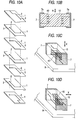
- FIG. 4B A further embodiment of the electronic part according to the present invention is shown in Fig. 4B.
- a multilayer body 24 has therein two or more sets of coil 40 arranged in a row. Both ends of each set of coil 40 are connected to respective terminal electrodes 20 formed on both ends of the multilayer body.
- the effects of improving dimensional accuracy and reducing property fluctuations can be obtained.
- inductors having this constitution necessitate a smaller mounting space than the same number of inductors separately fabricated.
- the structure shown in Fig. 4B can be modified so as to contain one or more built-in capacitors as in the structure shown in Fig. 3C.
- terminal electrode 20A1 and the intermediate terminal electrode 20A2 are served as input and output terminal and the terminal electrode 20A3 is served as a ground terminal so that the part shown in Fig. 8A can be used as an L-type filter.
- Fig. 8C is a sectional view and Fig. 8D shows an equivalent circuit of this embodiment.
- intermediate terminal electrodes 20A5 and 20A6 are provided at both ends of the coil 40 respectively between the terminal electrodes 20A4 and 20A7 which are placed at both ends of the multilayer body 24.
- the dielectric bodies 27 are provided between the intermediate terminal electrodes 20A5 and 20A6 and the terminal electrodes 20A4 and 20A6, respectively.
- the capacitor 28 is formed to compose a ⁇ -type filter circuit.
- Fig. 9A is a sectional view showing still another embodiment according to the present invention
- Fig. 9B shows an equivalent circuit thereof.
- Two pairs of electrodes 33 are provided between the terminal electrode 20A4 and the intermediate terminal electrode 20A5 and between the terminal electrode 20A7 and the intermediate terminal electrode 20A6.
- the electrodes 33 are respectively connected to terminal electrodes 20A4 to 20A7 through the leading conductors 30.
- Fig. 9C is a sectional view showing still another embodiment according to the present invention
- Fig. 9D shows an equivalent circuit thereof.
- an intermediate terminal electrode 20A9 is provided between terminal electrodes 20A8 and 20A10, and coils 40, 40 are provided at both sides of the intermediate terminal electrode 20A9.
- an internal electrode 34 constituting the capacitor 28 is provided so as to opposite to the intermediate terminal electrode 20A9.
- the internal electrode 34 and one of the coils 40 are connected through the leading conductor 29.
- the internal electrode 34 is connected to the other electrode 40 through a penetration conductor portion 32 provided in a non-conductor portion 31, which is formed by penetrating the intermediate terminal electrode 20A9 as a hole.
- a T-type filter as shown in Fig. 9D is structured.
- a magnetic element such as ferrite is used for the sheet 1. Further, the present invention can realize the multilayer body by not only sheet method but also printing method.
Landscapes
- Engineering & Computer Science (AREA)
- Power Engineering (AREA)
- Manufacturing & Machinery (AREA)
- Microelectronics & Electronic Packaging (AREA)
- Coils Or Transformers For Communication (AREA)
- Manufacturing Cores, Coils, And Magnets (AREA)
- Fixed Capacitors And Capacitor Manufacturing Machines (AREA)
- Filters And Equalizers (AREA)
Applications Claiming Priority (9)
| Application Number | Priority Date | Filing Date | Title |
|---|---|---|---|
| JP310310/96 | 1996-11-21 | ||
| JP31031096 | 1996-11-21 | ||
| JP31031096 | 1996-11-21 | ||
| JP117306/97 | 1997-05-07 | ||
| JP11730697 | 1997-05-07 | ||
| JP11730697 | 1997-05-07 | ||
| JP28416497A JP3438859B2 (ja) | 1996-11-21 | 1997-10-17 | 積層型電子部品とその製造方法 |
| JP28416497 | 1997-10-17 | ||
| JP284164/97 | 1997-10-17 |
Publications (3)
| Publication Number | Publication Date |
|---|---|
| EP0844625A2 true EP0844625A2 (fr) | 1998-05-27 |
| EP0844625A3 EP0844625A3 (fr) | 1999-02-10 |
| EP0844625B1 EP0844625B1 (fr) | 2003-03-12 |
Family
ID=27313352
Family Applications (1)
| Application Number | Title | Priority Date | Filing Date |
|---|---|---|---|
| EP97120473A Expired - Lifetime EP0844625B1 (fr) | 1996-11-21 | 1997-11-21 | Composant électronique multicouche et son procédé de fabrication |
Country Status (7)
| Country | Link |
|---|---|
| US (2) | US6147573A (fr) |
| EP (1) | EP0844625B1 (fr) |
| JP (1) | JP3438859B2 (fr) |
| CN (1) | CN1100329C (fr) |
| DE (1) | DE69719680T2 (fr) |
| MY (1) | MY119340A (fr) |
| NO (1) | NO975338L (fr) |
Cited By (10)
| Publication number | Priority date | Publication date | Assignee | Title |
|---|---|---|---|---|
| WO1999009568A1 (fr) * | 1997-08-21 | 1999-02-25 | Dale Electronics, Inc. | Inducteur multicouche a frequence d'autoresonance elevee et procede de fabrication de cet inducteur |
| EP1050959A2 (fr) * | 1999-05-07 | 2000-11-08 | Murata Manufacturing Co., Ltd. | Filtre LC stratifié |
| EP1050960A2 (fr) * | 1999-05-07 | 2000-11-08 | Murata Manufacturing Co., Ltd. | Filtre LC stratifié |
| EP1050958A2 (fr) * | 1999-05-07 | 2000-11-08 | Murata Manufacturing Co., Ltd. | Filtre LC à empilement |
| EP1152438A1 (fr) * | 1999-09-17 | 2001-11-07 | FDK Corporation | Bobine d'inductance multicouche et procede de fabrication de ladite bobine d'inductance |
| FR2809233A1 (fr) * | 2000-05-12 | 2001-11-23 | Murata Manufacturing Co | Composant electronique stratifie |
| EP1160972A2 (fr) * | 2000-05-31 | 2001-12-05 | TDK Corporation | Composants électroniques |
| CN100434919C (zh) * | 2006-04-20 | 2008-11-19 | 上海交通大学 | 用于探测癌细胞的生物磁感应压电传感阵列 |
| EP2720361A4 (fr) * | 2011-06-10 | 2015-09-30 | Murata Manufacturing Co | Convertisseur cc/cc de type multicanaux |
| US9824804B2 (en) | 2015-04-02 | 2017-11-21 | Tdk Corporation | Composite ferrite composition and electronic component |
Families Citing this family (50)
| Publication number | Priority date | Publication date | Assignee | Title |
|---|---|---|---|---|
| MY122218A (en) * | 1998-02-02 | 2006-03-31 | Taiyo Yuden Kk | Multilayer electronic component and manufacturing method therefor |
| WO1999046784A1 (fr) * | 1998-03-13 | 1999-09-16 | Matsushita Electric Industrial Co., Ltd. | Module et procede de fabrication correspondant |
| JP2910758B1 (ja) * | 1998-04-27 | 1999-06-23 | 株式会社村田製作所 | 積層型lc部品 |
| US6345434B1 (en) * | 1998-07-06 | 2002-02-12 | Tdk Corporation | Process of manufacturing an inductor device with stacked coil pattern units |
| US6820320B2 (en) * | 1998-07-06 | 2004-11-23 | Tdk Corporation | Process of making an inductor device |
| JP2001023822A (ja) * | 1999-07-07 | 2001-01-26 | Tdk Corp | 積層フェライトチップインダクタアレイおよびその製造方法 |
| US6512430B2 (en) * | 2000-06-29 | 2003-01-28 | Delphi Technologies, Inc. | Passive low pass filter |
| US6704248B1 (en) * | 2001-05-25 | 2004-03-09 | Lockheed Martin Corporation | High density power module incorporating passive components distributed in a substrate |
| JP3555598B2 (ja) * | 2001-06-27 | 2004-08-18 | 株式会社村田製作所 | 積層型インダクタ |
| JP4608821B2 (ja) * | 2001-06-28 | 2011-01-12 | Tdk株式会社 | 積層フィルタ |
| US20030024111A1 (en) * | 2001-08-02 | 2003-02-06 | Aem, Inc. | Dot penetration method for inter-layer connections of electronic components |
| JP2003051729A (ja) * | 2001-08-06 | 2003-02-21 | Tdk Corp | 積層型フィルタアレイ |
| US6911889B2 (en) * | 2001-08-20 | 2005-06-28 | Steward, Inc. | High frequency filter device and related methods |
| US6582990B2 (en) * | 2001-08-24 | 2003-06-24 | International Rectifier Corporation | Wafer level underfill and interconnect process |
| US20030042044A1 (en) * | 2001-08-30 | 2003-03-06 | Micron Technology, Inc. | Circuit board plane interleave apparatus and method |
| KR100423399B1 (ko) * | 2001-11-05 | 2004-03-18 | 삼성전기주식회사 | 다연 노이즈저감 필터 |
| US6975199B2 (en) * | 2001-12-13 | 2005-12-13 | International Business Machines Corporation | Embedded inductor and method of making |
| US7427904B2 (en) * | 2003-09-12 | 2008-09-23 | Avaya Inc. | Ultra-high-frequency notch filter having an inductance set by selecting a conductor width |
| US6931712B2 (en) * | 2004-01-14 | 2005-08-23 | International Business Machines Corporation | Method of forming a dielectric substrate having a multiturn inductor |
| DE112005001483B4 (de) * | 2004-06-21 | 2017-03-23 | Sekisui Chemical Co., Ltd. | Bindemittelharz-Zusammensetzung, und deren Verwendung als Paste und Grünfolie |
| JP4419728B2 (ja) * | 2004-07-12 | 2010-02-24 | 株式会社村田製作所 | 積層コイルアレイ |
| JP4736526B2 (ja) * | 2005-05-11 | 2011-07-27 | パナソニック株式会社 | コモンモードノイズフィルタ |
| JP2007012825A (ja) * | 2005-06-29 | 2007-01-18 | Ricoh Co Ltd | チップ部品及びその製造方法 |
| KR100663242B1 (ko) | 2005-06-29 | 2007-01-02 | 송만호 | 적층형 칩 타입 파워 인덕터 및 그 제조 방법 |
| CN101331564B (zh) * | 2005-12-23 | 2014-04-09 | 株式会社村田制作所 | 层叠线圈器件及其制造方法 |
| JP2008054287A (ja) * | 2006-07-27 | 2008-03-06 | Murata Mfg Co Ltd | ノイズフィルタアレイ |
| JP4821908B2 (ja) * | 2007-12-26 | 2011-11-24 | 株式会社村田製作所 | 積層型電子部品及びこれを備えた電子部品モジュール |
| CN101981635B (zh) * | 2008-04-08 | 2013-09-25 | 株式会社村田制作所 | 电子元器件 |
| JP2010040882A (ja) * | 2008-08-07 | 2010-02-18 | Murata Mfg Co Ltd | 電子部品 |
| CN102362320B (zh) * | 2009-03-26 | 2014-07-30 | 株式会社村田制作所 | 电子部件及其制造方法 |
| CN103069514A (zh) * | 2010-08-18 | 2013-04-24 | 株式会社村田制作所 | 电子部件及其制造方法 |
| JP5692502B2 (ja) * | 2010-09-09 | 2015-04-01 | Tdk株式会社 | インダクタを含む積層型電子部品 |
| TWM406265U (en) * | 2010-10-02 | 2011-06-21 | Domintech Co Ltd | Inductance IC chip packaging multi-layer substrate |
| JP5387542B2 (ja) * | 2010-11-09 | 2014-01-15 | 株式会社村田製作所 | 積層型lcフィルタ |
| KR101218985B1 (ko) * | 2011-05-31 | 2013-01-04 | 삼성전기주식회사 | 칩형 코일 부품 |
| WO2014061670A1 (fr) * | 2012-10-19 | 2014-04-24 | 株式会社村田製作所 | Dispositif de bobine stratifiée et son procédé de fabrication |
| JP5790702B2 (ja) | 2013-05-10 | 2015-10-07 | Tdk株式会社 | 複合フェライト組成物および電子部品 |
| KR101499719B1 (ko) * | 2013-08-09 | 2015-03-06 | 삼성전기주식회사 | 복합 전자부품 및 그 실장 기판 |
| JP6425375B2 (ja) * | 2013-10-11 | 2018-11-21 | 新光電気工業株式会社 | コイル基板及びその製造方法、インダクタ |
| US20150102891A1 (en) * | 2013-10-16 | 2015-04-16 | Samsung Electro-Mechanics Co., Ltd. | Chip electronic component, board having the same, and packaging unit thereof |
| JP2014239203A (ja) * | 2014-01-31 | 2014-12-18 | 株式会社村田製作所 | 電子部品及び電子部品の実装構造体 |
| JP6413278B2 (ja) * | 2014-03-25 | 2018-10-31 | Tdk株式会社 | チップ電子部品及びその製造方法 |
| JP6380546B2 (ja) * | 2014-09-29 | 2018-08-29 | 株式会社村田製作所 | Lcフィルタ |
| KR101658033B1 (ko) * | 2015-07-10 | 2016-09-30 | 룩씨스 주식회사 | 칩형 전자부품의 하드코팅 제조방법 |
| JP2019193074A (ja) * | 2018-04-24 | 2019-10-31 | Tdk株式会社 | 誘電体共振器および誘電体フィルタ |
| JP7020455B2 (ja) * | 2019-05-24 | 2022-02-16 | 株式会社村田製作所 | 積層型コイル部品 |
| JP7260015B2 (ja) * | 2019-05-24 | 2023-04-18 | 株式会社村田製作所 | 積層型コイル部品及びバイアスティー回路 |
| JP2020194804A (ja) * | 2019-05-24 | 2020-12-03 | 株式会社村田製作所 | 積層型コイル部品 |
| JP7260016B2 (ja) * | 2019-05-24 | 2023-04-18 | 株式会社村田製作所 | 積層型コイル部品 |
| CN115102581B (zh) * | 2022-06-21 | 2024-05-14 | 维沃移动通信有限公司 | 电子设备 |
Citations (3)
| Publication number | Priority date | Publication date | Assignee | Title |
|---|---|---|---|---|
| US5302932A (en) * | 1992-05-12 | 1994-04-12 | Dale Electronics, Inc. | Monolythic multilayer chip inductor and method for making same |
| JPH0855726A (ja) * | 1994-08-10 | 1996-02-27 | Taiyo Yuden Co Ltd | 積層型電子部品及びその製造方法 |
| US5497137A (en) * | 1993-12-17 | 1996-03-05 | Murata Manufacturing Co., Ltd. | Chip type transformer |
Family Cites Families (24)
| Publication number | Priority date | Publication date | Assignee | Title |
|---|---|---|---|---|
| US3812442A (en) * | 1972-02-29 | 1974-05-21 | W Muckelroy | Ceramic inductor |
| US3833872A (en) * | 1972-06-13 | 1974-09-03 | I Marcus | Microminiature monolithic ferroceramic transformer |
| JPS5821807A (ja) * | 1981-07-31 | 1983-02-08 | Tdk Corp | チツプインダクタ及びその製造方法 |
| JPS6261305A (ja) * | 1985-09-11 | 1987-03-18 | Murata Mfg Co Ltd | 積層チツプコイル |
| JPH0752257B2 (ja) * | 1988-08-04 | 1995-06-05 | 株式会社甲南カメラ研究所 | 眼球手術用顕微鏡 |
| JPH0693589B2 (ja) * | 1989-03-23 | 1994-11-16 | 株式会社村田製作所 | Lcフィルター |
| JP3186776B2 (ja) * | 1990-12-29 | 2001-07-11 | ティーディーケイ株式会社 | 電子部品の製造方法 |
| JPH081870B2 (ja) * | 1991-03-29 | 1996-01-10 | 太陽誘電株式会社 | セラミックインダクタの製造方法 |
| US5349743A (en) * | 1991-05-02 | 1994-09-27 | At&T Bell Laboratories | Method of making a multilayer monolithic magnet component |
| JP2958821B2 (ja) * | 1991-07-08 | 1999-10-06 | 株式会社村田製作所 | ソリッドインダクタ |
| JPH05152132A (ja) * | 1991-11-28 | 1993-06-18 | Murata Mfg Co Ltd | 積層型コイル |
| US5476728A (en) * | 1992-03-31 | 1995-12-19 | Tdk Corporation | Composite multilayer parts |
| JPH06216689A (ja) * | 1993-01-19 | 1994-08-05 | Murata Mfg Co Ltd | ディレイライン |
| US5583424A (en) * | 1993-03-15 | 1996-12-10 | Kabushiki Kaisha Toshiba | Magnetic element for power supply and dc-to-dc converter |
| JPH0722243A (ja) * | 1993-07-02 | 1995-01-24 | Murata Mfg Co Ltd | インダクタアレイ |
| US5609704A (en) * | 1993-09-21 | 1997-03-11 | Matsushita Electric Industrial Co., Ltd. | Method for fabricating an electronic part by intaglio printing |
| US5592134A (en) * | 1994-02-09 | 1997-01-07 | Mitsubishi Materials Corporation | EMI filter with a ceramic material having a chemical reaction inhibiting component |
| JPH0846471A (ja) * | 1994-07-29 | 1996-02-16 | Murata Mfg Co Ltd | 積層型lc複合部品 |
| US5647966A (en) * | 1994-10-04 | 1997-07-15 | Matsushita Electric Industrial Co., Ltd. | Method for producing a conductive pattern and method for producing a greensheet lamination body including the same |
| US5821846A (en) * | 1995-05-22 | 1998-10-13 | Steward, Inc. | High current ferrite electromagnetic interference suppressor and associated method |
| US5614757A (en) * | 1995-10-26 | 1997-03-25 | Dale Electronics, Inc. | Monolithic multilayer chip inductor having a no-connect terminal |
| US5948200A (en) * | 1996-07-26 | 1999-09-07 | Taiyo Yuden Co., Ltd. | Method of manufacturing laminated ceramic electronic parts |
| US6038134A (en) * | 1996-08-26 | 2000-03-14 | Johanson Dielectrics, Inc. | Modular capacitor/inductor structure |
| US5880662A (en) * | 1997-08-21 | 1999-03-09 | Dale Electronics, Inc. | High self resonant frequency multilayer inductor and method for making same |
-
1997
- 1997-10-17 JP JP28416497A patent/JP3438859B2/ja not_active Expired - Lifetime
- 1997-11-20 NO NO975338A patent/NO975338L/no not_active Application Discontinuation
- 1997-11-20 MY MYPI97005592A patent/MY119340A/en unknown
- 1997-11-21 US US08/975,458 patent/US6147573A/en not_active Expired - Lifetime
- 1997-11-21 EP EP97120473A patent/EP0844625B1/fr not_active Expired - Lifetime
- 1997-11-21 DE DE69719680T patent/DE69719680T2/de not_active Expired - Lifetime
- 1997-11-21 CN CN97126397A patent/CN1100329C/zh not_active Expired - Lifetime
-
2000
- 2000-02-24 US US09/512,643 patent/US6568054B1/en not_active Expired - Lifetime
Patent Citations (3)
| Publication number | Priority date | Publication date | Assignee | Title |
|---|---|---|---|---|
| US5302932A (en) * | 1992-05-12 | 1994-04-12 | Dale Electronics, Inc. | Monolythic multilayer chip inductor and method for making same |
| US5497137A (en) * | 1993-12-17 | 1996-03-05 | Murata Manufacturing Co., Ltd. | Chip type transformer |
| JPH0855726A (ja) * | 1994-08-10 | 1996-02-27 | Taiyo Yuden Co Ltd | 積層型電子部品及びその製造方法 |
Non-Patent Citations (1)
| Title |
|---|
| PATENT ABSTRACTS OF JAPAN vol. 096, no. 006, 28 June 1996 & JP 08 055726 A (TAIYO YUDEN CO LTD), 27 February 1996 * |
Cited By (16)
| Publication number | Priority date | Publication date | Assignee | Title |
|---|---|---|---|---|
| WO1999009568A1 (fr) * | 1997-08-21 | 1999-02-25 | Dale Electronics, Inc. | Inducteur multicouche a frequence d'autoresonance elevee et procede de fabrication de cet inducteur |
| EP1050958A3 (fr) * | 1999-05-07 | 2002-07-17 | Murata Manufacturing Co., Ltd. | Filtre LC à empilement |
| EP1050959A2 (fr) * | 1999-05-07 | 2000-11-08 | Murata Manufacturing Co., Ltd. | Filtre LC stratifié |
| EP1050960A2 (fr) * | 1999-05-07 | 2000-11-08 | Murata Manufacturing Co., Ltd. | Filtre LC stratifié |
| EP1050958A2 (fr) * | 1999-05-07 | 2000-11-08 | Murata Manufacturing Co., Ltd. | Filtre LC à empilement |
| EP1050960A3 (fr) * | 1999-05-07 | 2002-07-17 | Murata Manufacturing Co., Ltd. | Filtre LC stratifié |
| EP1050959A3 (fr) * | 1999-05-07 | 2002-07-17 | Murata Manufacturing Co., Ltd. | Filtre LC stratifié |
| EP1152438A1 (fr) * | 1999-09-17 | 2001-11-07 | FDK Corporation | Bobine d'inductance multicouche et procede de fabrication de ladite bobine d'inductance |
| EP1152438A4 (fr) * | 1999-09-17 | 2003-05-28 | Fdk Corp | Bobine d'inductance multicouche et procede de fabrication de ladite bobine d'inductance |
| FR2809233A1 (fr) * | 2000-05-12 | 2001-11-23 | Murata Manufacturing Co | Composant electronique stratifie |
| EP1160972A2 (fr) * | 2000-05-31 | 2001-12-05 | TDK Corporation | Composants électroniques |
| EP1160972A3 (fr) * | 2000-05-31 | 2003-09-17 | TDK Corporation | Composants électroniques |
| US6713162B2 (en) | 2000-05-31 | 2004-03-30 | Tdk Corporation | Electronic parts |
| CN100434919C (zh) * | 2006-04-20 | 2008-11-19 | 上海交通大学 | 用于探测癌细胞的生物磁感应压电传感阵列 |
| EP2720361A4 (fr) * | 2011-06-10 | 2015-09-30 | Murata Manufacturing Co | Convertisseur cc/cc de type multicanaux |
| US9824804B2 (en) | 2015-04-02 | 2017-11-21 | Tdk Corporation | Composite ferrite composition and electronic component |
Also Published As
| Publication number | Publication date |
|---|---|
| MY119340A (en) | 2005-05-31 |
| JP3438859B2 (ja) | 2003-08-18 |
| CN1100329C (zh) | 2003-01-29 |
| NO975338L (no) | 1998-05-22 |
| NO975338D0 (no) | 1997-11-20 |
| EP0844625A3 (fr) | 1999-02-10 |
| US6568054B1 (en) | 2003-05-27 |
| DE69719680D1 (de) | 2003-04-17 |
| DE69719680T2 (de) | 2003-08-14 |
| JPH1126241A (ja) | 1999-01-29 |
| US6147573A (en) | 2000-11-14 |
| CN1191376A (zh) | 1998-08-26 |
| EP0844625B1 (fr) | 2003-03-12 |
Similar Documents
| Publication | Publication Date | Title |
|---|---|---|
| EP0844625B1 (fr) | Composant électronique multicouche et son procédé de fabrication | |
| EP0433176B1 (fr) | Circuit hybride multi-couche | |
| EP0551735B1 (fr) | Inducteur de haute précision monté à la surface | |
| EP0134556B1 (fr) | Un élément d'impédance | |
| US6452473B1 (en) | Multilayer inductor and method of manufacturing the same | |
| US4904967A (en) | LC composite component | |
| EP0982742B1 (fr) | Module et procede de fabrication correspondant | |
| US6107907A (en) | High current ferrite electromagnetic interference supressor and associated method | |
| EP0953994A2 (fr) | Bobine multicouche et sa méthode de fabrication | |
| EP1538638A2 (fr) | Méthode de fabrication d'un composant électronique multi-couche et composant multicouche | |
| EP0836277A2 (fr) | Dispositif LC composite | |
| EP0793289A1 (fr) | Séparateur de fréquence multicouche | |
| KR20020077799A (ko) | 적층인덕터 | |
| US8355240B2 (en) | Multilayer capacitor and method for adjusting equivalent series impedance of same | |
| US6675462B1 (en) | Method of manufacturing a multi-laminated inductor | |
| US6249205B1 (en) | Surface mount inductor with flux gap and related fabrication methods | |
| US5436601A (en) | Laminated delay line | |
| JPH0897070A (ja) | セラミックコンデンサ | |
| US6621378B2 (en) | Filter | |
| EP0771013A1 (fr) | Inductance de puce monolithique multicouche ultramince et sa méthode de fabrication | |
| JP3554775B2 (ja) | 積層型コイル部品 | |
| EP1089302A1 (fr) | Bobine d'arrêt de mode commun pour montage en surface et son procédé de fabrication | |
| JP3320096B2 (ja) | 積層型インダクタおよびその製造方法 | |
| US6288626B1 (en) | Common mode choke including parallel conductors and associated methods | |
| JPH11260653A (ja) | 積層型電子部品とその製造方法 |
Legal Events
| Date | Code | Title | Description |
|---|---|---|---|
| PUAI | Public reference made under article 153(3) epc to a published international application that has entered the european phase |
Free format text: ORIGINAL CODE: 0009012 |
|
| AK | Designated contracting states |
Kind code of ref document: A2 Designated state(s): DE FR GB NL SE |
|
| AX | Request for extension of the european patent |
Free format text: AL;LT;LV;MK;RO;SI |
|
| PUAL | Search report despatched |
Free format text: ORIGINAL CODE: 0009013 |
|
| AK | Designated contracting states |
Kind code of ref document: A3 Designated state(s): AT BE CH DE DK ES FI FR GB GR IE IT LI LU MC NL PT SE |
|
| AX | Request for extension of the european patent |
Free format text: AL;LT;LV;MK;RO;SI |
|
| 17P | Request for examination filed |
Effective date: 19990805 |
|
| AKX | Designation fees paid |
Free format text: DE FR GB NL SE |
|
| 17Q | First examination report despatched |
Effective date: 20010511 |
|
| GRAH | Despatch of communication of intention to grant a patent |
Free format text: ORIGINAL CODE: EPIDOS IGRA |
|
| GRAH | Despatch of communication of intention to grant a patent |
Free format text: ORIGINAL CODE: EPIDOS IGRA |
|
| GRAA | (expected) grant |
Free format text: ORIGINAL CODE: 0009210 |
|
| AK | Designated contracting states |
Designated state(s): DE FR GB NL SE |
|
| REG | Reference to a national code |
Ref country code: GB Ref legal event code: FG4D |
|
| REF | Corresponds to: |
Ref document number: 69719680 Country of ref document: DE Date of ref document: 20030417 Kind code of ref document: P |
|
| REG | Reference to a national code |
Ref country code: SE Ref legal event code: TRGR |
|
| ET | Fr: translation filed | ||
| PLBE | No opposition filed within time limit |
Free format text: ORIGINAL CODE: 0009261 |
|
| STAA | Information on the status of an ep patent application or granted ep patent |
Free format text: STATUS: NO OPPOSITION FILED WITHIN TIME LIMIT |
|
| 26N | No opposition filed |
Effective date: 20031215 |
|
| PGFP | Annual fee paid to national office [announced via postgrant information from national office to epo] |
Ref country code: NL Payment date: 20041103 Year of fee payment: 8 |
|
| PGFP | Annual fee paid to national office [announced via postgrant information from national office to epo] |
Ref country code: SE Payment date: 20041105 Year of fee payment: 8 |
|
| PGFP | Annual fee paid to national office [announced via postgrant information from national office to epo] |
Ref country code: FR Payment date: 20041109 Year of fee payment: 8 |
|
| PGFP | Annual fee paid to national office [announced via postgrant information from national office to epo] |
Ref country code: GB Payment date: 20041117 Year of fee payment: 8 |
|
| PG25 | Lapsed in a contracting state [announced via postgrant information from national office to epo] |
Ref country code: GB Free format text: LAPSE BECAUSE OF NON-PAYMENT OF DUE FEES Effective date: 20051121 |
|
| PG25 | Lapsed in a contracting state [announced via postgrant information from national office to epo] |
Ref country code: SE Free format text: LAPSE BECAUSE OF NON-PAYMENT OF DUE FEES Effective date: 20051122 |
|
| PG25 | Lapsed in a contracting state [announced via postgrant information from national office to epo] |
Ref country code: NL Free format text: LAPSE BECAUSE OF NON-PAYMENT OF DUE FEES Effective date: 20060601 |
|
| EUG | Se: european patent has lapsed | ||
| GBPC | Gb: european patent ceased through non-payment of renewal fee |
Effective date: 20051121 |
|
| PG25 | Lapsed in a contracting state [announced via postgrant information from national office to epo] |
Ref country code: FR Free format text: LAPSE BECAUSE OF NON-PAYMENT OF DUE FEES Effective date: 20060731 |
|
| NLV4 | Nl: lapsed or anulled due to non-payment of the annual fee |
Effective date: 20060601 |
|
| REG | Reference to a national code |
Ref country code: FR Ref legal event code: ST Effective date: 20060731 |
|
| PGFP | Annual fee paid to national office [announced via postgrant information from national office to epo] |
Ref country code: DE Payment date: 20161116 Year of fee payment: 20 |
|
| REG | Reference to a national code |
Ref country code: DE Ref legal event code: R071 Ref document number: 69719680 Country of ref document: DE |