EP0843316A2 - Nichtflüchtige Halbleiterspeicheranordnung - Google Patents
Nichtflüchtige Halbleiterspeicheranordnung Download PDFInfo
- Publication number
- EP0843316A2 EP0843316A2 EP97308480A EP97308480A EP0843316A2 EP 0843316 A2 EP0843316 A2 EP 0843316A2 EP 97308480 A EP97308480 A EP 97308480A EP 97308480 A EP97308480 A EP 97308480A EP 0843316 A2 EP0843316 A2 EP 0843316A2
- Authority
- EP
- European Patent Office
- Prior art keywords
- blocks
- word lines
- transistors
- memory cell
- voltage
- Prior art date
- Legal status (The legal status is an assumption and is not a legal conclusion. Google has not performed a legal analysis and makes no representation as to the accuracy of the status listed.)
- Granted
Links
Images

Classifications
-
- G—PHYSICS
- G11—INFORMATION STORAGE
- G11C—STATIC STORES
- G11C8/00—Arrangements for selecting an address in a digital store
- G11C8/16—Multiple access memory array, e.g. addressing one storage element via at least two independent addressing line groups
-
- G—PHYSICS
- G11—INFORMATION STORAGE
- G11C—STATIC STORES
- G11C16/00—Erasable programmable read-only memories
- G11C16/02—Erasable programmable read-only memories electrically programmable
- G11C16/06—Auxiliary circuits, e.g. for writing into memory
- G11C16/08—Address circuits; Decoders; Word-line control circuits
-
- G—PHYSICS
- G11—INFORMATION STORAGE
- G11C—STATIC STORES
- G11C16/00—Erasable programmable read-only memories
- G11C16/02—Erasable programmable read-only memories electrically programmable
- G11C16/06—Auxiliary circuits, e.g. for writing into memory
- G11C16/10—Programming or data input circuits
-
- G—PHYSICS
- G11—INFORMATION STORAGE
- G11C—STATIC STORES
- G11C8/00—Arrangements for selecting an address in a digital store
- G11C8/14—Word line organisation; Word line lay-out
-
- G—PHYSICS
- G11—INFORMATION STORAGE
- G11C—STATIC STORES
- G11C2216/00—Indexing scheme relating to G11C16/00 and subgroups, for features not directly covered by these groups
- G11C2216/12—Reading and writing aspects of erasable programmable read-only memories
- G11C2216/22—Nonvolatile memory in which reading can be carried out from one memory bank or array whilst a word or sector in another bank or array is being erased or programmed simultaneously
-
- G—PHYSICS
- G11—INFORMATION STORAGE
- G11C—STATIC STORES
- G11C2216/00—Indexing scheme relating to G11C16/00 and subgroups, for features not directly covered by these groups
- G11C2216/12—Reading and writing aspects of erasable programmable read-only memories
- G11C2216/24—Nonvolatile memory in which programming can be carried out in one memory bank or array whilst a word or sector in another bank or array is being erased simultaneously
-
- G—PHYSICS
- G11—INFORMATION STORAGE
- G11C—STATIC STORES
- G11C8/00—Arrangements for selecting an address in a digital store
- G11C8/10—Decoders
Definitions
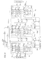
- the above-mentioned semiconductor memory device further includes a storage circuit whose stored content is variable, and a transistor switching voltage output circuit for selectively outputting the transistor ON or OFF voltage in accordance with the content stored in the storage circuit.
- the invention described herein makes possible the advantage of providing a non-volatile semiconductor memory device in which data can be read from one memory cell array block while data is being written in or erased from another memory cell array block on one chip, with the increase in chip layout area being minimized.
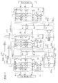
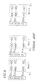
- Figure 3 is a block diagram of the third example according to the present invention.
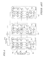
- the gate control voltages G 2 , ..., G K-1 of the MOS transistor groups MOS 2 to MOS K-1 between the other memory cell array blocks BL 2 to BL K reach a voltage V XX level, and each transistor of the MOS transistor groups MOS 2 to MOS K-1 is turned on.
- the word lines are electrically connected to each other between the memory cell array blocks BL 2 to BL K .
- Gate voltages L 3 , ..., L K of the P-channel MOS transistors between the global word lines and the local word lines in the other blocks are set, for example, at 10 volts so as to turn off the P-channel MOS transistors.
- the setting of each gate voltage L 1 , ..., L K is controlled based on the information specifying the blocks to be operated in parallel and the information indicating which operation (i.e., the read, write, or erase operation) is performed in the blocks.
Landscapes
- Engineering & Computer Science (AREA)
- Microelectronics & Electronic Packaging (AREA)
- Read Only Memory (AREA)
- Non-Volatile Memory (AREA)
Applications Claiming Priority (3)
| Application Number | Priority Date | Filing Date | Title |
|---|---|---|---|
| JP302269/96 | 1996-11-14 | ||
| JP30226996 | 1996-11-14 | ||
| JP30226996A JPH10144086A (ja) | 1996-11-14 | 1996-11-14 | 不揮発性半導体記憶装置 |
Publications (3)
| Publication Number | Publication Date |
|---|---|
| EP0843316A2 true EP0843316A2 (de) | 1998-05-20 |
| EP0843316A3 EP0843316A3 (de) | 1999-05-19 |
| EP0843316B1 EP0843316B1 (de) | 2003-12-10 |
Family
ID=17906986
Family Applications (1)
| Application Number | Title | Priority Date | Filing Date |
|---|---|---|---|
| EP97308480A Expired - Lifetime EP0843316B1 (de) | 1996-11-14 | 1997-10-23 | Nichtflüchtige Halbleiterspeicheranordnung |
Country Status (6)
| Country | Link |
|---|---|
| US (1) | US6081450A (de) |
| EP (1) | EP0843316B1 (de) |
| JP (1) | JPH10144086A (de) |
| KR (1) | KR100287131B1 (de) |
| DE (1) | DE69726698T2 (de) |
| TW (1) | TW355844B (de) |
Cited By (7)
| Publication number | Priority date | Publication date | Assignee | Title |
|---|---|---|---|---|
| WO2001069603A2 (en) * | 2000-03-15 | 2001-09-20 | Advanced Micro Devices, Inc. | Multiple bank simultaneous operation for a flash memory |
| EP1143455A2 (de) * | 2000-03-29 | 2001-10-10 | Sharp Kabushiki Kaisha | Nichtflüchtige Halbleiterspeicheranordnung |
| WO2003007306A2 (en) * | 2001-07-11 | 2003-01-23 | Sun Microsystems, Inc. | Method and system for banking register file memory arrays |
| WO2003025937A2 (en) * | 2001-09-17 | 2003-03-27 | Sandisk Corporation | Background operation for memory cells |
| EP1721321A2 (de) * | 2004-02-04 | 2006-11-15 | Atmel Corporation | Nichtflüchtige speichermatrix mit dem merkmal von gleichzeitigem schreiben und löschen |
| EP1727153A1 (de) * | 2005-05-25 | 2006-11-29 | STMicroelectronics S.r.l. | Entladeschaltung für einen wortweise löschbaren Flash-Speicher |
| US7660156B2 (en) | 2001-09-17 | 2010-02-09 | Sandisk Corporation | NAND flash memory with a programming voltage held dynamically in a NAND chain channel region |
Families Citing this family (20)
| Publication number | Priority date | Publication date | Assignee | Title |
|---|---|---|---|---|
| JP3940513B2 (ja) | 1999-01-11 | 2007-07-04 | 株式会社東芝 | 半導体記憶装置 |
| KR100560634B1 (ko) * | 1999-01-13 | 2006-03-16 | 삼성전자주식회사 | 불휘발성 반도체 메모리 장치 |
| EP1052646B1 (de) | 1999-05-11 | 2004-07-14 | Fujitsu Limited | Nichtflüchtige Halbleiterspeicheranordnung, die eine Datenleseoperation während einer Datenschreib/lösch-Operation erlaubt |
| US6163478A (en) * | 1999-10-19 | 2000-12-19 | Advanced Micro Devices, Inc. | Common flash interface implementation for a simultaneous operation flash memory device |
| US6851026B1 (en) * | 2000-07-28 | 2005-02-01 | Micron Technology, Inc. | Synchronous flash memory with concurrent write and read operation |
| KR100368590B1 (ko) * | 2000-04-17 | 2003-01-24 | 삼성전자 주식회사 | 비등분할 메모리 블록을 가진 반도체 메모리 장치 |
| JP3871184B2 (ja) | 2000-06-12 | 2007-01-24 | シャープ株式会社 | 半導体記憶装置 |
| US7184307B2 (en) * | 2001-08-28 | 2007-02-27 | Samsung Electronics Co., Ltd. | Flash memory device capable of preventing program disturbance according to partial programming |
| US20050185465A1 (en) * | 2003-03-11 | 2005-08-25 | Fujitsu Limited | Memory device |
| JP2005116119A (ja) | 2003-10-10 | 2005-04-28 | Toshiba Corp | 不揮発性半導体記憶装置 |
| US7058754B2 (en) * | 2003-12-22 | 2006-06-06 | Silicon Storage Technology, Inc. | Nonvolatile memory device capable of simultaneous erase and program of different blocks |
| KR100610006B1 (ko) * | 2004-05-04 | 2006-08-08 | 삼성전자주식회사 | 호스트 시스템의 다중동작 지원에 적합한 메모리 구조를갖는 반도체 메모리 장치 |
| JP2007128633A (ja) * | 2005-10-07 | 2007-05-24 | Matsushita Electric Ind Co Ltd | 半導体記憶装置及びこれを備えた送受信システム |
| JP2007157331A (ja) * | 2007-03-16 | 2007-06-21 | Ricoh Co Ltd | 複合化フラッシュメモリ及びそれを搭載した携帯用機器 |
| KR20110131208A (ko) * | 2009-02-09 | 2011-12-06 | 램버스 인코포레이티드 | 동기화된 제어를 갖는 다중 플레인의 비휘발성 메모리 |
| WO2012160821A1 (ja) | 2011-05-24 | 2012-11-29 | パナソニック株式会社 | 抵抗変化型不揮発性記憶装置および抵抗変化型不揮発性記憶装置の駆動方法 |
| CN102918600B (zh) | 2011-05-31 | 2014-11-19 | 松下电器产业株式会社 | 电阻变化型非易失性存储装置 |
| KR102586179B1 (ko) * | 2018-10-04 | 2023-10-10 | 에스케이하이닉스 주식회사 | 반도체 장치 |
| CN112634955A (zh) * | 2019-09-24 | 2021-04-09 | 长鑫存储技术有限公司 | Dram存储器 |
| JP2023141465A (ja) * | 2022-03-24 | 2023-10-05 | キオクシア株式会社 | 半導体記憶装置 |
Citations (4)
| Publication number | Priority date | Publication date | Assignee | Title |
|---|---|---|---|---|
| EP0478251A2 (de) * | 1990-09-26 | 1992-04-01 | STMicroelectronics, Inc. | Halbleiterspeicheranordnung mit verriegelten Zwischenverstärkern für Speicherzeilenleitungsauswahl |
| JPH0554682A (ja) * | 1991-08-29 | 1993-03-05 | Mitsubishi Electric Corp | 不揮発性半導体メモリ |
| US5448517A (en) * | 1987-06-29 | 1995-09-05 | Kabushiki Kaisha Toshiba | Electrically programmable nonvolatile semiconductor memory device with NAND cell structure |
| WO1996034391A1 (en) * | 1995-04-28 | 1996-10-31 | Intel Corporation | Nonvolatile memory blocking architecture and redundancy |
Family Cites Families (1)
| Publication number | Priority date | Publication date | Assignee | Title |
|---|---|---|---|---|
| EP0741415A1 (de) * | 1995-05-05 | 1996-11-06 | STMicroelectronics S.r.l. | Flash-EEPROM-Speicher mit kontaktlosen Speicherzellen |
-
1996
- 1996-11-14 JP JP30226996A patent/JPH10144086A/ja active Pending
-
1997
- 1997-10-08 US US08/947,086 patent/US6081450A/en not_active Expired - Lifetime
- 1997-10-13 TW TW086114962A patent/TW355844B/zh not_active IP Right Cessation
- 1997-10-23 EP EP97308480A patent/EP0843316B1/de not_active Expired - Lifetime
- 1997-10-23 DE DE69726698T patent/DE69726698T2/de not_active Expired - Lifetime
- 1997-11-14 KR KR1019970063579A patent/KR100287131B1/ko not_active IP Right Cessation
Patent Citations (4)
| Publication number | Priority date | Publication date | Assignee | Title |
|---|---|---|---|---|
| US5448517A (en) * | 1987-06-29 | 1995-09-05 | Kabushiki Kaisha Toshiba | Electrically programmable nonvolatile semiconductor memory device with NAND cell structure |
| EP0478251A2 (de) * | 1990-09-26 | 1992-04-01 | STMicroelectronics, Inc. | Halbleiterspeicheranordnung mit verriegelten Zwischenverstärkern für Speicherzeilenleitungsauswahl |
| JPH0554682A (ja) * | 1991-08-29 | 1993-03-05 | Mitsubishi Electric Corp | 不揮発性半導体メモリ |
| WO1996034391A1 (en) * | 1995-04-28 | 1996-10-31 | Intel Corporation | Nonvolatile memory blocking architecture and redundancy |
Non-Patent Citations (2)
| Title |
|---|
| KRUECKEBERG J: "ZWEIGETEILTES EEPROM: GLEICHZEITIG AUSLESEN UND BESCHREIBEN" ELEKTRONIK, vol. 39, no. 26, 21 December 1990, pages 56-59, XP000177694 * |
| PATENT ABSTRACTS OF JAPAN vol. 017, no. 369 (P-1572), 12 July 1993 & JP 05 054682 A (MITSUBISHI ELECTRIC CORP), 5 March 1993 * |
Cited By (19)
| Publication number | Priority date | Publication date | Assignee | Title |
|---|---|---|---|---|
| WO2001069603A3 (en) * | 2000-03-15 | 2002-02-21 | Advanced Micro Devices Inc | Multiple bank simultaneous operation for a flash memory |
| WO2001069603A2 (en) * | 2000-03-15 | 2001-09-20 | Advanced Micro Devices, Inc. | Multiple bank simultaneous operation for a flash memory |
| EP1143455A3 (de) * | 2000-03-29 | 2004-02-25 | Sharp Kabushiki Kaisha | Nichtflüchtige Halbleiterspeicheranordnung |
| EP1143455A2 (de) * | 2000-03-29 | 2001-10-10 | Sharp Kabushiki Kaisha | Nichtflüchtige Halbleiterspeicheranordnung |
| US6469928B2 (en) | 2000-03-29 | 2002-10-22 | Sharp Kabushiki Kaisha | Nonvolatile semiconductor memory device with concurrent memory access and data locking |
| WO2003007306A2 (en) * | 2001-07-11 | 2003-01-23 | Sun Microsystems, Inc. | Method and system for banking register file memory arrays |
| WO2003007306A3 (en) * | 2001-07-11 | 2003-11-27 | Sun Microsystems Inc | Method and system for banking register file memory arrays |
| US7660156B2 (en) | 2001-09-17 | 2010-02-09 | Sandisk Corporation | NAND flash memory with a programming voltage held dynamically in a NAND chain channel region |
| WO2003025937A3 (en) * | 2001-09-17 | 2003-11-27 | Sandisk Corp | Background operation for memory cells |
| WO2003025937A2 (en) * | 2001-09-17 | 2003-03-27 | Sandisk Corporation | Background operation for memory cells |
| US6741502B1 (en) | 2001-09-17 | 2004-05-25 | Sandisk Corporation | Background operation for memory cells |
| US6845045B1 (en) | 2001-09-17 | 2005-01-18 | Sandisk Corporation | Background operation for memory cells |
| EP1701355A2 (de) * | 2001-09-17 | 2006-09-13 | SanDisk Corporation | Hintergrundbetrieb für Speicherzellen |
| US7978533B2 (en) | 2001-09-17 | 2011-07-12 | Sandisk Corporation | NAND flash memory with a programming voltage held dynamically in a NAND chain channel region |
| EP1701355A3 (de) * | 2001-09-17 | 2007-02-14 | SanDisk Corporation | Hintergrundbetrieb für Speicherzellen |
| EP1721321A2 (de) * | 2004-02-04 | 2006-11-15 | Atmel Corporation | Nichtflüchtige speichermatrix mit dem merkmal von gleichzeitigem schreiben und löschen |
| EP1721321A4 (de) * | 2004-02-04 | 2007-02-28 | Atmel Corp | Nichtflüchtige speichermatrix mit dem merkmal von gleichzeitigem schreiben und löschen |
| US7580289B2 (en) | 2005-05-25 | 2009-08-25 | Stmicroelectronics, S.R.L. | Discharge circuit for a word-erasable flash memory device |
| EP1727153A1 (de) * | 2005-05-25 | 2006-11-29 | STMicroelectronics S.r.l. | Entladeschaltung für einen wortweise löschbaren Flash-Speicher |
Also Published As
| Publication number | Publication date |
|---|---|
| KR100287131B1 (ko) | 2001-04-16 |
| US6081450A (en) | 2000-06-27 |
| KR19980042858A (ko) | 1998-08-17 |
| JPH10144086A (ja) | 1998-05-29 |
| DE69726698D1 (de) | 2004-01-22 |
| DE69726698T2 (de) | 2004-10-07 |
| EP0843316B1 (de) | 2003-12-10 |
| EP0843316A3 (de) | 1999-05-19 |
| TW355844B (en) | 1999-04-11 |
Similar Documents
| Publication | Publication Date | Title |
|---|---|---|
| US6081450A (en) | Non-volatile semiconductor memory device in which read, write and erase operations can be simultaneously performed in different memory cell array blocks | |
| KR100392301B1 (ko) | 비휘발성 반도체 기억 장치 | |
| US5109361A (en) | Electrically page erasable and programmable read only memory | |
| KR100394756B1 (ko) | 비휘발성 반도체 기억 장치 | |
| US4543647A (en) | Electrically programmable non-volatile semiconductor memory device | |
| US7355903B2 (en) | Semiconductor device including memory cells and current limiter | |
| KR20000064879A (ko) | 비휘발성 메모리구조 | |
| JP4703162B2 (ja) | 不揮発性半導体記憶装置及びその書き込み方法 | |
| US6785182B2 (en) | Nonvolatile semiconductor memory device | |
| JP3165489B2 (ja) | 持久メモリアレイに対するバイアス回路 | |
| KR20040015897A (ko) | 비트라인 커플링과 로딩 효과에 대해 안정적인 소스라인을 갖는 플레쉬 메모리 어레이 | |
| EP0495493B1 (de) | Nichtflüchtige, elektrisch löschbare Halbleiterspeicheranordnungen | |
| US7248503B2 (en) | Semiconductor nonvolatile storage device | |
| US20040196695A1 (en) | Nonvolatile memory device and semiconductor device | |
| US20030189858A1 (en) | Method and apparatus for emulating an electrically erasable programmable read only memory (EEPROM) using non-volatile floating gate memory cells | |
| US7436716B2 (en) | Nonvolatile memory | |
| EP0498336A1 (de) | Verbindung mit gemeinsamer Leitung für ein integriertes Speicher-Array | |
| US6775186B1 (en) | Low voltage sensing circuit for non-volatile memory device | |
| JPH097364A (ja) | 半導体記憶装置 | |
| JPH0785685A (ja) | 半導体装置 | |
| US6385091B1 (en) | Read reference scheme for non-volatile memory | |
| US6195295B1 (en) | Segmented column memory device voltage steering technique | |
| JPH0629499A (ja) | 半導体記憶装置 | |
| JP3362917B2 (ja) | 半導体メモリ装置 | |
| JPH04228192A (ja) | 不揮発性記憶セルアレイの語線に電源電圧とプログラミング電圧を印加する語線駆動回路 |
Legal Events
| Date | Code | Title | Description |
|---|---|---|---|
| PUAI | Public reference made under article 153(3) epc to a published international application that has entered the european phase |
Free format text: ORIGINAL CODE: 0009012 |
|
| AK | Designated contracting states |
Kind code of ref document: A2 Designated state(s): DE FR GB |
|
| PUAL | Search report despatched |
Free format text: ORIGINAL CODE: 0009013 |
|
| AK | Designated contracting states |
Kind code of ref document: A3 Designated state(s): AT BE CH DE DK ES FI FR GB GR IE IT LI LU MC NL PT SE |
|
| 17P | Request for examination filed |
Effective date: 19991117 |
|
| AKX | Designation fees paid |
Free format text: DE FR GB |
|
| 17Q | First examination report despatched |
Effective date: 20020516 |
|
| GRAH | Despatch of communication of intention to grant a patent |
Free format text: ORIGINAL CODE: EPIDOS IGRA |
|
| GRAS | Grant fee paid |
Free format text: ORIGINAL CODE: EPIDOSNIGR3 |
|
| GRAA | (expected) grant |
Free format text: ORIGINAL CODE: 0009210 |
|
| AK | Designated contracting states |
Kind code of ref document: B1 Designated state(s): DE FR GB |
|
| REG | Reference to a national code |
Ref country code: GB Ref legal event code: FG4D |
|
| REF | Corresponds to: |
Ref document number: 69726698 Country of ref document: DE Date of ref document: 20040122 Kind code of ref document: P |
|
| ET | Fr: translation filed | ||
| PLBE | No opposition filed within time limit |
Free format text: ORIGINAL CODE: 0009261 |
|
| STAA | Information on the status of an ep patent application or granted ep patent |
Free format text: STATUS: NO OPPOSITION FILED WITHIN TIME LIMIT |
|
| 26N | No opposition filed |
Effective date: 20040913 |
|
| PGFP | Annual fee paid to national office [announced via postgrant information from national office to epo] |
Ref country code: FR Payment date: 20121018 Year of fee payment: 16 Ref country code: DE Payment date: 20121017 Year of fee payment: 16 |
|
| PGFP | Annual fee paid to national office [announced via postgrant information from national office to epo] |
Ref country code: GB Payment date: 20121017 Year of fee payment: 16 |
|
| GBPC | Gb: european patent ceased through non-payment of renewal fee |
Effective date: 20131023 |
|
| PG25 | Lapsed in a contracting state [announced via postgrant information from national office to epo] |
Ref country code: GB Free format text: LAPSE BECAUSE OF NON-PAYMENT OF DUE FEES Effective date: 20131023 |
|
| REG | Reference to a national code |
Ref country code: DE Ref legal event code: R119 Ref document number: 69726698 Country of ref document: DE Effective date: 20140501 |
|
| REG | Reference to a national code |
Ref country code: FR Ref legal event code: ST Effective date: 20140630 |
|
| PG25 | Lapsed in a contracting state [announced via postgrant information from national office to epo] |
Ref country code: FR Free format text: LAPSE BECAUSE OF NON-PAYMENT OF DUE FEES Effective date: 20131031 Ref country code: DE Free format text: LAPSE BECAUSE OF NON-PAYMENT OF DUE FEES Effective date: 20140501 |