EP0840449A2 - Digitale Wellenformerschaltung, Schaltungsanordnung zur Frequenzvervielfachung, Verfahren und Schaltung zur Aussensynchronisierung - Google Patents
Digitale Wellenformerschaltung, Schaltungsanordnung zur Frequenzvervielfachung, Verfahren und Schaltung zur Aussensynchronisierung Download PDFInfo
- Publication number
- EP0840449A2 EP0840449A2 EP97118804A EP97118804A EP0840449A2 EP 0840449 A2 EP0840449 A2 EP 0840449A2 EP 97118804 A EP97118804 A EP 97118804A EP 97118804 A EP97118804 A EP 97118804A EP 0840449 A2 EP0840449 A2 EP 0840449A2
- Authority
- EP
- European Patent Office
- Prior art keywords
- circuit
- output
- cycle
- signal
- duty
- Prior art date
- Legal status (The legal status is an assumption and is not a legal conclusion. Google has not performed a legal analysis and makes no representation as to the accuracy of the status listed.)
- Withdrawn
Links
Images


Classifications
-
- H—ELECTRICITY
- H03—ELECTRONIC CIRCUITRY
- H03K—PULSE TECHNIQUE
- H03K5/00—Manipulating of pulses not covered by one of the other main groups of this subclass
- H03K5/01—Shaping pulses
- H03K5/04—Shaping pulses by increasing duration; by decreasing duration
- H03K5/05—Shaping pulses by increasing duration; by decreasing duration by the use of clock signals or other time reference signals
-
- H—ELECTRICITY
- H04—ELECTRIC COMMUNICATION TECHNIQUE
- H04L—TRANSMISSION OF DIGITAL INFORMATION, e.g. TELEGRAPHIC COMMUNICATION
- H04L7/00—Arrangements for synchronising receiver with transmitter
- H04L7/02—Speed or phase control by the received code signals, the signals containing no special synchronisation information
-
- H—ELECTRICITY
- H03—ELECTRONIC CIRCUITRY
- H03K—PULSE TECHNIQUE
- H03K5/00—Manipulating of pulses not covered by one of the other main groups of this subclass
- H03K5/00006—Changing the frequency
-
- H—ELECTRICITY
- H03—ELECTRONIC CIRCUITRY
- H03K—PULSE TECHNIQUE
- H03K5/00—Manipulating of pulses not covered by one of the other main groups of this subclass
- H03K5/156—Arrangements in which a continuous pulse train is transformed into a train having a desired pattern
- H03K5/1565—Arrangements in which a continuous pulse train is transformed into a train having a desired pattern the output pulses having a constant duty cycle
Definitions
- the present invention relates to a digital wave shaping circuit, a frequency multiplying circuit, and an external synchronizing method and external synchronizing circuit, which produce digital signals, the phase of which is identical to the phase position of external trigger signals with the frequency thereof identical to the frequency of digital input signals.
- the interruption frequency of semiconductor active elements is definite, and the usable maximum frequency is subject to the limitation thereof.
- the wave forms of digital signals (1) and (2) are identical to each other in the repeating frequency f.
- the ratio of the upside H level period TA and the downside L level period TB is not 1:1 while in the wave form of signal (1) the ratio of period TA and period TB the wave form of signal (1) is 1:1 (duty 50%), the apparent (virtual) frequency f is increased.
- the wave form of input signal is broken from a state of duty 50% (signal (1)) to a state of smaller duty wave form (signal (2)) than the state in a case where an IC of semiconductor active element is caused to receive an input wave form of duty 50% signal (1) and operates at the extremely upper level of its operatable period, a signal of frequency exceeding the operatable period is inputted into the corresponding IC, thereby causing the corresponding IC not to function in response to the frequency of the corresponding input signals.
- digital signals to be handled have a wave form for which the ratio of period TA and period TB is 1:1 (duty 50%).
- digital signals to be handled are shaped to a wave form of duty 50% at all times, it will be possible to handle signals of higher frequencies by using the semiconductor active elements.
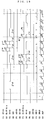
- a synchronizing signal selection circuit (disclosed by Japanese Patent Publication No.95606 of 1986) shown in FIG.22 is constructed as a circuit in which the reference signal So of a frequency "m" times the repeating frequency f ("m" is an integral number including and more than 2) of repeating frequency f of the required synchronizing output signal is received, and "n" sub reference signals Sa, Sb, Sc of different phases ("n” is an integral number including and more than 2) are produced by gradually shifting the phase of the reference signal by delay elements DL1, DL2, wherein, since trigger signal G is received, these sub reference signals are commenced to be frequency-divided by frequency dividers 823, 824, 825, and the frequency-divided signals are logically synthesized in a logic circuit 822, thereby causing the output to be picked up as a synchronizing output signal.
- the jitter is decreased in compliance with the number of the phase divisions, that is, the number "n" of the sub reference signals.
- n sub reference signals Sa, Sb, Sc of different phases from the reference signal So.
- a number of delay elements DL1, DL2,... are connected in series and are produced by carrying out an operation of gradually shifting the phases of the reference signal with the reference signal supplied into the delay elements.
- the jitter is decreased responsive to the number "n" of phase divisions, that is, sub reference signals. Therefore, in a case where a lower frequency (for example, 1MHz or the like) is handled, the number of delay elements to be prepared is 2,000 to 3,000, wherein it is disadvantageous in the economical aspect and in view of heating of the elements.
- an actual wave form shaping circuit which is able to operate waves is constructed with as a few number of semiconductor elements as possible.
- the jitter is decreased responsive to the number "n" of phase divisions, that is, sub reference signals. Therefore, in a case where a lower frequency (for example, 1MHz or the like) is handled, the number of delay elements to be prepared is 2,000 to 3,000, wherein it is disadvantageous in the economical aspect and in view of heating of the elements.
- an external synchronizing circuit which is able to pick up clock signals synchronized with the trigger signals by using as a few number of semiconductor elements as possible.
- an actual external synchronizing circuit which is simple in construction, causes input clock signals to synchronize with external trigger signals and outputs signals in a state where the input digital signals are shaped to wave form of duty 50% and an actual external synchronizing method are proposed.
- an external synchronizing method and external synchronizing circuit are proposed, which automatically cause output clocks to synchronize with external trigger signals even though the external trigger signals are fluctuated.
- the first object of the invention is to provide a wave form shaping circuit which outputs signals after the wave forms of input signals are shaped to those of duty 50% regardless of whether or not the input signals are of duty 50%.
- the invention is constructed as shown below.
- One aspect of the present invention is a digital wave shaping circuit comprising: a timing generation circuit for generating a required timing signal from an input clock signal; a duty determination circuit for determining and instructing the timing position of duty 50% of a clock signal to be outputted, upon receiving the timing signal generated by the timing generation circuit, which is composed of a cycle measurement circuit for measuring the length of one cycle in the first cycle arriving at every interval of integral number times of one cycle of the input clock signal, an operation circuit for calculating the length of one half of one cycle on the basis of the value thereof, an actual measurement circuit for executing measurement of the length in each cycle of input clock signals, and a coincidence circuit for outputting a coincidence output as said timing position of duty 50% when the corresponding measured value becomes coincident with said calculated value; and a width forming circuit for generating and outputting a clock signal having a pulse width corresponding to said duty 50% on the basis of a signal synchronized with the front edge of the input clock signal EXT-CK and the timing position determined and instructed by said duty determination circuit.
- the digital wave shaping circuit of this invention is a circuit which takes out a signal frequency of which is the same as that of the original signal.
- the cycle measurement circuit measures the length of one cycle in the first cycle arriving at every interval of integral number times of one cycle of the input clock signal.
- the operation circuit calculates the value equivalent to the half length of one cycle.
- the measurement of the length is executed in the actual measurement circuit in each cycle of input clock signals, and a coincidence output is outputted from the coincidence circuit when the corresponding measured value becomes coincident with the above-mentioned calculated value. This coincidence output indicates the above-mentioned timing position of duty 50%.
- a pulse is risen up by a signal synchronized with the front edge of input clock signal and is fallen at a timing position, that is, by a coincident signal, which is designated and determined in the duty determination circuit, whereby it is possible to form and output clock signals having a pulse width equivalent to the above-mentioned duty 50%.
- a digital wave shaping circuit comprising: a timing generation circuit for generating, from input clock signals, required timing signals including a signal for instructing the target measurement period to be measured as length of one cycle of the input clock signals with an interval which is integral number times one cycle of the input clock signal, a signal for instructing an actual measurement period for sustaining a measurement operation over the target measurement period, a signal for defining an oscillation reference period commencing from the front edge of an input clock signal and ending before arriving at the front edge of the next input clock; a cycle measurement circuit having a delay line oscillator for oscillating only during the actual measurement period upon receiving a signal of the actual measurement period produced in the timing generation circuit, a counter for counting the number of cycles of oscillation of the corresponding delay line oscillator, and a latch circuit for latching the value of the corresponding counter when said target measurement period ends; an operation circuit for calculating the half value of the count value latched in said cycle measurement circuit by using the count value; an actual measurement circuit having a delay line oscillator
- a digital wave shaping circuit comprising: a timing generation circuit for generating required timing signals from an input clock signal of a fixed cycle; a first and a second duty determination circuits for determining and instructing the timing position of duty 50% of a clock signal to be outputted, upon receiving said timing signal, which operate with at least one cycle overlapped with and with two cycles shifted from each other; wherein said first and second duty determination circuits have a delay line oscillator, a counter for counting the number of cycles of oscillation, an operation circuit for calculating the half value of the counted value, and a coincidence circuit which uses output of the corresponding operation circuit as one input and uses output of said counter as the other input, said first duty determination circuit measures the length of one cycle by causing the delay line oscillator to oscillate and counting the number of cycles of oscillation by the counter in the first cycle arriving at every interval of integral number times of one cycle of the input clock signal, executes measurement of the length from the front edge of each cycle by causing the delay line oscillator to oscillate and
- a first and a second duty determination circuits which are overlapped with each other at least one cycle and operate with two cycles shifted from each other are used, wherein coincidence outputs showing the timing position of the above-mentioned duty 50% are obtained from the respective duty determination circuits.
- width forming circuit a pulse is risen up by a signal synchronized with the front edge of input clock signal and is fallen by the above-mentioned coincidence outputs, whereby it is possible to output clock signals having a pulse width equivalent to duty 50%.
- the first and second duty determination circuits which are overlapped with each other at least one cycle and operate with two cycles shifted from each other are used, wherein coincidence outputs showing the timing position of the above-mentioned duty 50% are obtained from the respective duty determination circuits, the target measurement period and actual measurement period are clearly distinguished, it is possible to securely perform oscillating actions in the target measurement period fully to the width of one cycle.
- a digital wave shaping circuit comprising: a timing generation circuit for generating, from input clock signals, required timing signals including a signal for instructing the target measurement period to be measured as length of the one cycle of the input clock signal with an interval which is integral number times one cycle of the input clock signal, and a signal for instructing an actual measurement period to sustain a measurement operation slightly longer than the target measurement period; a first and a second duty determination circuits for determining and instructing a timing position of duty 50% of a clock signal to be outputted, upon receiving said timing signal, each of which is constructed to have a delay line oscillator, a counter for counting the number of cycles of the oscillation, an operation circuit for calculating the half value of the counted value and a coincidence circuit which uses output of the corresponding operation circuit as one input and uses output of said counter as the other input, and which operate with at least one cycle overlapped with and with two cycles shifted from each other; a first flip flop positioned before said first duty determination circuit, which is set every time in synchron
- output of the above-mentioned pre-positioned flip flops is inputted into the duty determination circuits attached thereto and is inputted in the output side.
- the above-mentioned pre-positioned flip flops are reset to cause the signal to the output side to disappear, thereby adverse influences can be avoided.
- signals indicating the actual measurement periods are securely inputted in the duty determination circuit attached thereto via OR gates. That is, a common delay line oscillator, etc. which constitute one duty determination circuit can be operated without fail by changing them to the actual measurement period or oscillation reference period. Therefore, the construction is further simplified in comparison with a case where two pairs of delay line oscillator, etc. are provided for the actual measurement periods and oscillation reference periods.
- a digital wave shaping circuit comprising: a timing generation circuit for generating, from input clock signals, required timing signals including a signal for instructing the target measurement period to be measured as length of the one cycle of the input clock signal with an interval which is integral number times one cycle of the input clock signal, and a signal for instructing an actual measurement period to sustain a measurement operation slightly longer than the target measurement period; a first and a second duty determination circuits for determining and instructing a timing position of duty 50% of a clock signal to be outputted, upon receiving said timing signal, each of which is constructed to have a delay line oscillator, a counter for counting the number of cycles of the oscillation, an operation circuit for calculating the half value of the counted value and a coincidence circuit which uses output of the corresponding operation circuit as one input and uses output of said counter as the other input, and which operate with at least one cycle overlapped with and with two cycles shifted form each other; a first flip flop positioned before said first duty determination circuit, which is set every time in synchron
- Another aspect of the present invention is a frequency multiplying circuit comprising: a timing generation circuit for generating, from input clock signals, required timing signals including a signal for instructing the target measurement period to be measured as length of the one cycle of an input clock signal with an interval which is integral number times one cycle of the input clock signal, and a signal for instructing an actual measurement period to sustain a measurement operation slightly longer than the target measurement period; and a first duty determination circuit and a second duty determination circuit for determining and instructing a timing position of duty 50% of a clock signal to be outputted, upon receiving said timing signal, which operate with at least one cycle overlapped with and with two cycles shifted from each other; wherein both duty determination circuits respectively include a delay line oscillator, a counter for counting the number of cycles of the oscillation, an operation circuit for calculating 1/4 value, 2/4 value, and 3/4 value of the counted value, and a coincidence circuit which uses said three results of the calculation of the corresponding operation circuit as one input thereof, uses the output of said counter as the other input thereof and outputs
- the length of one cycle is measured.
- the operation circuit calculates the timing value of a one-fourth value, a two-fourth value, and a third-fourth value of the calculated value, that is, the duty of 25%, 50% and 75%.
- the length is measured and, when the corresponding measured value becomes coincident with the above-mentioned calculated three values (1/4, 2/4, and 3/4 of the calculated value), coincidence outputs are outputted from the coincidence circuits. These coincidence outputs show the timing position of the above-mentioned duties 25%, 50% and 75%.
- a pulse is risen up by a signal synchronized with the front edge of the input clock signal and is gradually risen up and fallen at the timing positions indicated and determined by the above-mentioned duty determination circuit, that is, the timing positions of duties 25%, 50% and 75%. Therefore, it is possible to form and output clock signals of a pulse wave form for which the frequency is two times the input signal and the duty thereof is 50%.
- the input clock signals have any optional frequency or cycle length, or the input clock signals are of a wave form, the duty of which is fluctuating, it is possible to obtain multiplied outputs, the wave form of which is duty 50%, as output at all times. That is, clock signals of pulse wave form for which the frequency is two times the input clock signals and the duty is 50% can be outputted at all times. Therefore, it is possible to increase the apparent frequency limit of semiconductor active elements used.
- the first and second duty determination circuits which are overlapped at least one cycle with each other and operate with two cycles shifted from each other are used, and flip flops and OR gates are positioned before each of them. Therefore, at the time of oscillation in the actual measurement period, the output of the above-mentioned pre-positioned flip flops are inputted into the duty determination circuits attached thereto and are inputted in the output side. As the final coincidence output is generated, the above-mentioned pre-positioned flip flops are reset to cause the signals toward the output side to disappear and the influences toward the output side can be avoided. Moreover, signals indicating the actual measurement periods are securely inputted in the duty determination circuits via OR gates. That is, the common delay line circuit, etc. which constitute one duty determination circuit are operated by changing over in the actual measurement period and oscillation reference period. Therefore, the construction is further simplified in comparison with two pairs of delay line oscillators, etc. for the actual measurement period and oscillation reference period.
- the first and second duty determination circuit which is overlapped at least one cycle with each other and operates with two cycles shifted from each other, since coincident signals showing the timing positions duty 25%, 50% and 75% are outputted by turns, the target measurement period and actual measurement period are clearly distinguished, whereby it is possible to securely perform an action of oscillation in the target measurement period to the full width of one cycle.
- the construction is further simple in comparison with a case where two pairs of delay line circuits, etc. for the actual measurement periods and oscillation reference periods.
- Another aspect of the present invention is a n external synchronizing method for synchronizing an input clock signal with an external trigger signal, comprising steps of: producing a number of internal trigger signals synchronized with an external trigger signal according to a cycle of input clock signals until the next external trigger signal arrives; sharing them, with timing shifted from each other, to the first duty determination circuit and the second duty determination circuit; measuring alternately the timing position corresponding to duty 50% of a cycle of input clock signal from the position of the internal trigger signal; causing an output pulse to rise up at the position of the internal trigger signal; and causing the output pulse to fall at the timing position corresponding to said measured duty 50%.
- Another aspect of the present invention is a n external synchronizing circuit comprising: an internal trigger generating circuit which, upon receiving a timing signal from timing generation circuit 301, measures a phase position from an external trigger signal at one cycle T of input clock signal, generates and outputs an internal trigger signal at a phase position corresponding to the phase position, at which the external trigger signal arrives, at each of the next one cycle T; a mode change signal generation circuit for outputting internal trigger signals, sharing them to the first group signals and the second group signals, in each period of the external trigger signals, upon receiving said internal trigger signal; a first flip flop operating upon receiving said first group signals and a second flip flop operating upon receiving said second group signals; a first duty determination circuit which executes oscillation upon receiving the output of said first flip flop, determines the timing position of duty 50% of a clock signal to be outputted, by counting the number of cycles of the oscillation, outputs the coincidence output indicating the timing position, and resets said first flip flop; a second duty determination circuit which executes oscillation upon receiving the output
- a number of internal trigger signals synchronized with the external trigger signals are produced at cycles of input clock signals until the next external trigger signals arrive, and are shared to the first duty determination circuit and the second duty determination circuit with the timing shifted from each other, wherein the timing positions corresponding to duty 50% of the cycle of input clock signals are measured from the position of the internal trigger signals, the output pulse is risen up at the position of the internal trigger signals and the output pulse is fallen at the timing positions corresponding to the above-mentioned measured duty 50%. Since the internal trigger signals are inherently generated at cycles of the input clock signals in addition to the external trigger signals, output pulses can be easily obtained in synchronization with this signal.
- Another aspect of the present invention is a n external synchronizing circuit comprising: an internal trigger generation circuit which, upon receiving a timing signal from a timing generation circuit, measures a phase position from an external trigger signal in one cycle (T) of input clock signal, prepares the reference internal trigger signal at the phase position corresponding to the phase position, at which the external trigger signal arrives, in every next one cycle (T), alternately shares the signal to "A" period of external trigger signal and "B” period of it adjacent to said period, and outputs it as an internal trigger signal; an "A" side mode change signal generation circuit which, upon receiving one of said internal trigger signals, outputs the internal trigger signals in said "A" period sharing the them to the first group signals and second group signals; a first flip flop operating upon receiving said "A" side first group signal (SET-A1) and a second flip flop operating upon receiving said second group signal (SET-A2); a first duty determination circuit which executes oscillation upon receiving the output of said "A" side first flip flop, determines a timing position of a duty
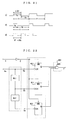
- FIG. 1 is a view showing first preferred embodiment of a digital wave shaping circuit according to the invention.
- FIG.2 is a timing chart showing operations of major parts of the circuit illustrated in FIG. 1.
- FIG.3 is a view showing a second preferred embodiment of the digital wave shaping circuit according to the invention.
- FIG.4 is a timing chart showing operations of major parts of the circuit illustrated in FIG.3.
- FIG.5 is a view showing a third preferred embodiment of the digital wave shaping circuit according to the invention.
- FIG.6 is a timing chart showing operations of major parts of the circuit illustrated in FIG.5.
- FIG.7 is a view showing a preferred embodiment of a frequency multiplying circuit according to the invention.
- FIG.8 is a timing chart showing operations of major parts of the circuit illustrated in FIG.7.
- FIG.9 is a view showing the left half part of a circuit of the first preferred embodiment of an external synchronizing circuit according to the invention.
- FIG.10 is a view showing the right half part of a circuit of the first preferred embodiment of an external synchronizing circuit according to the invention.
- FIG.11 is a timing chart showing operations of major parts of the circuit illustrated in FIG.9 and FIG.10.
- FIG.12 is an enlarged view showing the upper half part of the timing chart of FIG.11.
- FIG.13 is an enlarged view showing the lower half part of the timing chart of FIG.11.
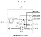
- FIG.14 is a circuitry diagram showing a detailed example of timing generation circuit 302 illustrated in FIG.9.
- FIG.15 is a timing chart showing operations of part of timing generation circuit 302 illustrated in FIG.9 and a mode change signal generation circuit.
- FIG.16 is a timing chart showing operations of part of a duty determination circuit of FIG.18 and a width forming circuit.
- FIG.17 is an enlarged view of the upper half part of the timing chart illustrated in FIG.16.
- FIG.18 is an enlarged view of the lower half part of the timing chart illustrated in FIG.16.
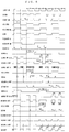
- FIG.19 is a exemplary view showing CKFA and CKFB which are produced by timing generation circuit 301 illustrated in FIG.9, wherein (a) thereof shows a case where they are made coincident with one cycle of input clock, and (b) thereof shows a case where they are made coincident with two cycles of input clock.
- FIG.20 is a view showing another preferred embodiment of the external synchronizing circuit of the invention.
- FIG.21 is a view prepared for description of fluctuations of frequency handled by semiconductor active elements.
- FIG.22 is a view showing the configuration of a phase-dividedpart used for a conventional synchronizing signal selection circuit.
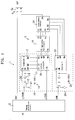
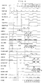
- Digital wave shaping circuit shown in FIG.1 has a timing generation circuit 2 which generates required timing signals CKF, 1/2CKW, 1/2CK, CKW from input clock signals CK, a duty determination circuit 3 which determines and indicates timing positions of an required duty values (herein, duty 50%) of a clock signal to be outputted, upon receiving timing signals 1/2CKW, 1/2CK, CKW generated by the timing generation circuit 2, and a width forming circuit 5 which forms and outputs clock signals (RS-FFQ) having a pulse width equivalent to the above-mentioned duty 50% on the basis of the timing positions determined and indicated by the duty determination circuit 3.
- a timing generation circuit 2 which generates required timing signals CKF, 1/2CKW, 1/2CK, CKW from input clock signals CK
- a duty determination circuit 3 which determines and indicates timing positions of an required duty values (herein, duty 50%) of a clock signal to be outputted, upon receiving timing signals 1/2CKW, 1/2CK, CKW generated by the timing generation circuit 2, and a width forming circuit 5 which forms and outputs clock
- CK is a clock signal inputted into the timing generation circuit 2 in which the duty may fluctuate while the repeating frequency is fixed (Cycle T).
- input clock signal CK is exaggeratedly depicted as a wave form in which the duty is fluctuating.
- Timing generation circuit 2 generates required timing signals CKF, 1/2CKW, 1/2CK, and CKW shown in FIG.2, from the input clock signal CK.
- CKF is a timing signal consisting of short pulses generated at the front edge of the input clock signal CK and is used as input of RS flip flop (hereinafter called RS-FF) 5a which constitutes a width forming circuit 5.
- RS-FF RS flip flop
- 1/2CK is a timing signal for specifying a period T1 (target measurement period) to be measured as a length of one cycle T of the input clock signal CK, and in details, this is a signal which can be obtained by dividing the input clock signal CK to one half. To establish the target measurement period, one cycle period T1 in odd numbers of the signal 1/2CK may be utilized.
- 1/2CKW is a timing signal to establish a period (actual measurement period) T3 to sustain a measurement operation over the above-mentioned target measurement period T1.
- This 1/2CKW is a signal the fall of which is slightly delayed from the above-mentioned 1/2CK, that is, a signal which is risen up simultaneously with the input clock CK, fallen after the fall of 1/2CK, having a slightly longer than one cycle T of the input clock signal CK.
- 1/2CKW can be obtained, for example, by producing a signal in which 1/2CK is slightly delayed in the width of 1/2 cycle thereof, and taking a logic sum of this signal and 1/2CK.
- CKW is a signal for defining an oscillation reference period, which is commenced from the front edge of signal CK and is terminated just before arriving the front edge of the next input clock, whenever every clock signal CK arrives, and is a timing signal for establishing the period (oscillation reference period )T4 for actually measuring the timing position of duty 50%.
- this CKW is risen up simultaneously with commencement of one cycle period T1 of odd numbers of the above-mentioned 1/2CK and termination of one cycle period T2 of even numbers of the above-mentioned 1/2CK, and is in HIGH level until the half of the corresponding period T1 and T2 (the timing position of duty 50%) passes, and thereafter the CKW is fallen before the termination of the corresponding period T1 and before commencement of the corresponding period T2.
- Duty determination circuit 3 is equipped with a cycle measurement circuit 10 which measures the length of one cycle period T1 of odd numbers upon receiving the above-mentioned timing signal 1/2CKW, a operation circuit 19 which calculates the half value of the corresponding one cycle length T1 of odd numbers, that is, the timing position of duty 50%, upon receiving the measurement result, and an actual measurement circuit 20 for actually measuring the timing position of duty 50% with respect to signal CK while CKW is in HIGH level, upon receiving the above-mentioned timing signal CKW.
- a cycle measurement circuit 10 which measures the length of one cycle period T1 of odd numbers upon receiving the above-mentioned timing signal 1/2CKW
- a operation circuit 19 which calculates the half value of the corresponding one cycle length T1 of odd numbers, that is, the timing position of duty 50%, upon receiving the measurement result
- an actual measurement circuit 20 for actually measuring the timing position of duty 50% with respect to signal CK while CKW is in HIGH level, upon receiving the above-mentioned timing signal CKW.
- the cycle measurement circuit 10 consists of a delay line oscillator 11, a counter 17, and a latch circuit 18, wherein the operation circuit 19 receives a parallel output of the latch circuit 18 and the parallel output is received by a coincidence circuit 28.
- Delay line oscillator 11 is composed of an NAND gate 12, one input terminal of which receives the above-mentioned timing signal 1/2CKW, an odd tier C-MOS inverter 13 which is connected to the output terminal of the corresponding NAND gate 12 as a delay element, and a simple reversing inverter 15 inserted into a feedback loop 14 from the output terminal of the corresponding inverter 13 to the other input terminal of the above-mentioned NAND gate.
- ECL inverter As an inverter 13 which is a delay element, ECL inverter, IIL inverter, etc. may be used in addition to the C-MOS inverter.
- the delay line oscillator 11 receives a timing signal 1/2CKW (actual measurement period T3) from the above-mentioned timing generation circuit 2, begins oscillating for measurement at the rise-up of the 1/2 CKW, and stops oscillating at the fall of it. That is, usually, NAND gate 12 is in such a state where one input terminal thereof is in a logic level L with the output thereof at H, and the output of inverter 15 (the other input terminal of NAND gate 12) is H while the output of inverter 13 is L, and the oscillation of the delay line oscillator 11 remains stopped.
- 1/2CKW actual measurement period T3
- NAND gate 12 usually, as one input terminal of NAND gate 12 is changed to logic level H, the status thereof changes, wherein the output of NAND gate 12 becomes L, the output of inverter 13 becomes H, the output of inverter 15 becomes L, the other input terminal of NAND gate 12 becomes H, and the output of NAND gate 12 becomes H, and the oscillation starts. Thereafter, the oscillation of the delay line oscillator 11 comes to a stop when the 1/2 CKW (actual measurement period T3) is fallen.
- the 1/2CKW (actual measurement period T3) is risen tip simultaneously with a rise-up of the above-mentioned timing signal 1/2CK (target measurement period T1), but it is fallen with a delay from a fall of the timing signal 1/2CK.
- this delay line oscillator 11 starts oscillating at a fall of the timing signal 1/2CK obtained by dividing the above-mentioned input clock signal CK to one half (at the commencement of the target measurement period T1) and stops oscillating after the 1/2CK is fallen (after termination of the target measurement period T1). Therefore, the oscillation is sustained during one cycle (target measurement period T1) of each odd number of the timing signal 1/2CK.
- Counter 17 counts a change of output DL-OSC1 of the above-mentioned delay line oscillator 11, that is, an output change generated once per cycle of oscillation, since the clock input terminal CK thereof is connected to the output terminal of the above-mentioned delay line oscillator 11. Furthermore, the above-mentioned timing signal 1/2CKW (actual measurement period T3) is inputted into a clear terminal CL of the counter 17.
- the counter 17 begins counting simultaneously with a rise-up of the above-mentioned timing signal 1/2CK (target measurement period T1) and stops counting after the point of time when the timing signal 1/2CK (target measurement period T1) is fallen as in operation of oscillation and stop of a delay line oscillator 11, whereby the counting of number of cycles of oscillation is sustained during one cycle period of each odd number of the timing signal 1/2CK (target measurement period T1).
- a figure output of the above-mentioned counter 17 is inputted into the latch circuit 18, and the timing signal 1/2CK (target measurement period T1) generated by the above-mentioned timing generation circuit 2 is inputted into the clock input terminal CK.
- this latch circuit 18 latches a count value (number of cycles of oscillation) of the counter 17 on the point of time when the timing signal 1/2CK (target measurement period T1) is fallen, that is, when the target measurement period T1 is terminated.
- the latch circuit 18 latches a count value of the number of cycles of oscillation corresponding to the length of one cycle period of each odd number of the timing signal 1/2CK (target measurement period T1) (one cycle T of the input clock signal CK).
- the operation circuit 19 calculates the half value of count value of the number of cycles of oscillations for one cycle of odd numbers of the timing signal 1/2CK (target measurement period T1) that is, the duty value of 50%, upon receiving the output of the above-mentioned latch circuit 18. This value becomes one input of the coincidence circuit 28.
- Actual measurement circuit 20 has a delay line oscillator 21 constructed to be like the above-mentioned cycle measurement circuit 10 and a second counter 27.
- the delay line oscillator 21 and the second counter 27 receive the above-mentioned timing signal CKW. Therefore, the delay line oscillator 21 sustains oscillation while the CKW is in H level (the oscillation reference period T4).
- the counter 27 counts the number of cycles of oscillation of the delay line oscillator 21 for the period T4 where this oscillation is being carried out.
- the count value passes through the timing position of duty 50% with respect to signal CK halfway of the counting.
- Coincidence circuit 28 uses a calculated value equivalent to duty 50% obtained from the above-mentioned operation circuit 19 as one input and uses the count value obtained from the above-mentioned counter 17 as the other input, wherein both are verified.
- the first duty determination circuit 3 determines the timing position of an required duty value (duty 50%) of a clock signal to be outputted and indicates the timing position to the width forming circuit 5 as a coincidence output.
- Width forming circuit 5 receives the above-mentioned timing signal CKF at a set input terminal S of RS-FF 5a thereof and receives the above-mentioned coincidence output SA at the reset input terminal R thereof. Therefore, the RS-FF 5a of the width forming circuit 5 is set by a timing signal CKF generated at the front edge per cycle of input clock signals CK and is reset by a coincidence output SA generated at the timing position of duty 50%.
- the input clock signal CK may be outputted (RS-FFQ) without fail after being shaped to a clear clock signal having a duty 50% wave form by causing the signal CK to pass through the digital wave shaping circuit 1.
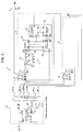
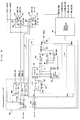
- FIG.3 shows the second embodiment which is provided with two pairs of duty determination circuits 3,4 having the same structure, wherein both the circuits are constructed, as shown as operation cycles C1,C2 in FIG.4, so that they alternately operate with two cycles of input clock signals EXT-CK shifted from each other.
- the first duty determination circuit 3 is called “A” side
- the second duty determination circuit 4 is called “B” side, and they are distinguished by respectively attaching affixes A and B thereto.
- the first duty determination circuit 3 handles, as shown in FIG.4, every four cycles (4T) of input clock signals EXT-CK as one repeating unit (operation cycle C1), measure the length T1A ("A" side target measurement period) of one cycle of the input clock signal EXT-CK at the first cycle (t1) of the front half thereof, and calculate the latter half value (timing position of duty 50%) of the length T of one cycle, using the result of the measurement, wherein on the basis thereof, at the third cycle (t3) and fourth cycle (t4) of the subsequent latter halves respectively, the first duty determination circuit 3 measures the length T5A from the front edge of the input clock signals EXT-CK until becoming coincident with the calculated value (that is, to the timing position of duty 50%), and, when the coincidence is secured, outputs a coincidence output SA indicating the timing position of duty 50%.
- the second duty determination circuit 4 has an operation cycle C2 shifted two cycles from the first duty determination circuit 3. That is, the second duty determination circuit 4 handles every four cycles (4T) of input clock signals EXT-CK shown with t3 through t6 in FIG.4 as one repeating unit (operation cycle C2), measures the length T1B ("B" side target measurement period) of one cycle of input clock signal EXT-CK at the first cycle (t3) of the front half thereof, and calculates the half value (timing position of duty 50%) of the length T of one cycle, using the result of the measurement, wherein on the basis thereof, at the third cycle (t5) and fourth cycle (t6) of the subsequent latter halves respectively, the second duty determination circuit 4 measures the length T5B from the front edge of the input clock signals EXT-CK until becoming coincident with the calculated value (that is, to the timing position of duty 50%), and, when the coincidence is secured, outputs a coincidence output SB indicating the timing position of duty 50%.
- operation cycle C2 shifted two cycles from the first duty determination
- the above-mentioned respective duty determination circuits 3,4 are constructed so that one pair of the delay line oscillator 11, counter 17 and latch circuit 18 concurrently achieves both the functions of the above-mentioned cycle measurement circuit 10 and actual measurement circuit 20, simplifying the construction of the duty determination circuit 3 described with reference to FIG.1. That is, in view of circuits, they are in a form of omitting the above-mentioned actual measurement circuit 20, wherein the operation circuit 19 is connected to the latch circuit 18 while the coincidence circuit 28 uses output of the operation circuit 19 as one input and uses output of the counter 17 as the other input.
- RS-FF 6 is positioned before the first duty determination circuit 3, and the Q output of RS-FF 6 is inputted into the delay line oscillator 11 of the duty determination circuit 3 through OR gate 7 (OR-A) and simultaneously is inputted into one input terminal of the OR gate 5b. And the output of the above-mentioned coincidence circuit 28, that is, the output of the duty determination circuit 3 is inputted into the reset terminal R positioned before the circuit 3.
- This OR gate 5b and RS-FF 6 constitute a width forming circuit 5.
- This RS-FF 6 is set by a short pulse SET-A ((9) in FIG.4) generated at the front edge of input clock signal EXT-CK in a case where QN ((8) in FIG.4) of JK-FF in the timing generation circuit 2 is H, that is, where the "A" side is in the oscillation reference period, and is reset by the above-mentioned coincidence output SA ((15) in FIG.4)(See (11) in FIG.4).
- pulses P1, P2 generated at the output terminal Q of RS-FF 6 at the third cycle t3 and the fourth cycle t4 is caused to appear in the output (OUT) via the OR gate 5b.
- RS-FF 8 and OR gate 9 are positioned before circuit 4, the Q output of RS-FF 8 is inputted into the delay line oscillator 11 of the duty determination circuit 4 through the OR gate 9 (OR-B), and simultaneously is inputted into the other input terminal of the OR gate 5b, wherein the output of the above-mentioned coincidence circuit 28, that is, the output of the duty determination circuit 4 is inputted into the reset terminal R of RS-FF 8 positioned before the circuit 4.
- This RS-FF 8 also constitutes a width forming circuit 5b along with the OR gate 5b.
- This RS-FF 8 is set by a short pulse SET-B ((16) in FIG.4) generated at the front edge of the input clock signal EXT-CK in a case where the Q ((7) in FIG.4) of JK-FF in the timing generation circuit 2 is H, that is, where the "B" side is in the oscillation generation period, and is reset by the above-mentioned coincidence output SB ((21) in FIG.4) (See ((18) in FIG.4).
- pulses P3, P4 generated at the output terminal Q of RS-FF 8 at the fifth cycle t5 and the sixth cycle t6 are caused to appear in the output (OUT) through the OR gate 5b.
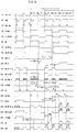
- Timing generation circuit 2 internally produces timing signals SET-AB, 1/2CK, 1/2CK-DL, WC,JK-FF-Q, and JK-FF-QN, and further using them, produces and outputs timing signals SET-A, SET-B, 1/2CKA, 1/2CKB, WC-A, and WC-B.
- SET-AB ((3) in FIG.4) is a timing signal consisting of short pulses generated at the front edge of the input clock signal EXT-CK.
- 1/2CK ((4) in FIG.4) is a timing signal for specifying a period T1 (target measurement period) to be measured as a length of one cycle T of the input clock signal EXT-CK, and concretely is a signal obtained by dividing the input clock signal EXT-CK to one half.
- WC ((6) in FIG.4) is a timing signal for establishing periods T3A, T3B (actual measurement periods) to sustain a measurement operation over the above-mentioned target measurement period T1.
- This WC is a signal, the fall of which is slightly delayed from the above-mentioned 1/2CK, that is, a signal, which is risen up simultaneously with the input clock CK, having a width which is slightly longer than one cycle T of the input clock signal EXT-CK.
- This WC is obtained by producing a signal 1/2CK-DL ((5) in FIG.4) in which 1/2CK is slightly delayed in the width of the 1/2 cycle thereof and taking a logic sum of the signal and 1/2CK.
- JK-FF-Q ((7) in FIG.4) is a signal of Q output of JK-FF in the timing generation circuit 2, and, when the Q output is H, indicates that the "A" side is in the measurement period (while the "B” side is in the oscillation reference period), and when the Q output N of JK-FF in the timing generation circuit 2 is H, JK-FF QN ((8) in FIG.4) indicates that the "B" side is in the measurement period (while the "A” side is in the oscillation reference period).
- SET-A ((9) in FIG.4) is a timing signal consisting of short pulses generated at the front edge of the input clock signal EXT-CK in a case where QN ((8) in F1G.4) of JK-FF in the timing generation circuit 2 is H, that is, where the "A" side is in the oscillation reference period, and will be a set input of the "A" side RS-FF 6.
- SET-B ((16) in FIG.4) is a timing signal consisting of short pulses generated at the front edge of input clock signal EXT-CK in a case where Q ((7) in FIG.4) of JK-FF in the timing generation circuit 2 is H, that is, where the "B" side is in the oscillation reference period and becomes a set input of RS-FF 8 at the "B" side.
- 1/2CKA ((14) in FIG.4) is a signal for establishing the "A" side target measurement period T1A, and is a signal which is taken out from 1/2CK while Q ((7) in FIG.4) of JK-FF in the timing generation circuit 2 is H, that is, while the "A" side is in the measurement period (while the "B” side is in the oscillation reference period).
- 1/2CKB ((20) in FIG.4) is a signal for establishing the "B" side target measurement period T1B and is a signal which is taken out from 1/2CK while QN((8) in FIG.4) of JK-FF in the timing generation circuit 2 is H, that is, while the "B" side is in the measurement period (while the "A” side is in the oscillation period).
- these signals are generated from input clock signal EXT-CK so that target measurement periods T1A, T1B to be measured as a length of the one cycle T are indicated with intervals T6A, T6B spaced, which are an integral number times, herein, three times one cycle T of the input clock signal EXT-CK.
- WC-A and WC-B are timing signals for actual measurement periods T3A, T3B and have a longer pulse than T1.
- input clock signal EXT-CK enters into the timing generation circuit 2.
- the timing generation circuit 2 begins dividing input clock signal EXT-CK to one half, wherein the Q output ((7) in FIG.4) of JK-FF is in H level at the point of time when the first SET-AB of the first cycle t1 is generated ("a" in FIG.4), and thereby the "A" side duty determination circuit 3 is selected and instructed so as to start measurement.
- the timing signal WC-A ((10) in FIG.4) is inputted into delay line oscillator 11 through OR gate 7 to commence the oscillation and is inputted into a clear terminal CL of the counter 17.
- the counter 17 begins counting the number of cycles of oscillation.
- the oscillation of the delay line oscillator 11 is sustained at least until the rise-up of a clock of the second cycle t2 is completed.
- the oscillation of the delay line oscillator 11 is terminated by a fall of WC-A produced until a rise-up of a clock of the third cycle t3, that is, at the time when the actual measurement period T3A slightly elapsed from one cycle T of the input clock CK ends (point "c" in FIG.4).
- the operation circuit 19 calculates one half of the count value of length of one cycle T, that is, the timing position of duty 50%, upon receiving output of the latch circuit 18, and outputs the result of the calculation, wherein the result is inputted into one input terminals B1 to Bn of the coincidence circuit 28.
- RS-FF 6 is set by arrival of SET-A ((9) in FIG.4) ("d" point in FIG.4).
- the set Q output ((11) in FIG.4) of RS-FF 6 is caused to appear in the output OUT through OR gate 5b, and simultaneously is added to the "A" side delay line oscillator 11 through OR gate 7, thereby causing the oscillator 11 to oscillate.
- the set Q output of RS-FF 6 is added to the clear CL of the "A" side counter 17 through the OR gate 7 to cleared the counter 17, causing the counting of the number of cycles of oscillation to commence.
- the output of counter 17 is inputted into the other input terminals A1 to An of the coincidence circuit 28, wherein the count value of the counter 17 is progressively increased, and at the moment ("e" point in FIG.4) when the count value is made coincident with the value (half the length of one cycle T) outputted by the above-mentioned operation circuit 19, a coincidence output SA is generated from the coincidence circuit 28.
- This coincidence output SA is inputted into the reset input terminal QN of RS-FF 6 and resets the flip flop. Therefore, when this coincidence output SA is generated, the set Q output ((11) in FIG.4) of RS-FF 6 is fallen and appears at the OR gate 5b as pulse P1.
- this output pulse P1 is a pulse which is risen up at the front edge of external input clock, that is, the input clock signal EXT-CK having one cycle T and is thereafter fallen at the position of the half (duty 50%) of the length T of one cycle.
- RS-FF 6 is set.
- the set Q output ((11) in FIG.4) of RS-FF 6 is added to the "A" side delay line oscillator 11 through OR gate 7 to cause it to oscillate, and is added to the counter 17 to clear it, causing the counting of the number of cycles of oscillation to commence, while the set Q output appears in the output OUT through OR gate 5b.
- a coincidence output SA is generated again from the coincidence circuit 28. Since RS-FF 6 is reset by this coincidence output SA, the set Q output ((11) in FIG.4) of RS-FF 6 is fallen and is caused to appear at OR gate 5b as pulse P2. As a matter of course, this output P2 is also a pulse which is risen up at the front edge of the external input clock, that is, the input clock signal EXT-CK and is fallen at the position of duty 50%.
- the timing signal WC-B ((17) in FIG.4) is risen up ("h" point in FIG.4), and is added to the "B" side delay line oscillator 11 through OR gate 9, whereby the oscillation is commenced. Simultaneously, the signal WC-B is inputted into a clear terminal CL of the counter 17, the rise-up of which causes the counter 17 to commence the countering of the number of cycles of oscillation.
- the oscillation of the "B" side delay line oscillator 11 is continued at least until a rise-up of the clock of the fourth cycle t4 is completed.
- the oscillation of the "B" side delay line oscillator 11 is terminated by a fall of WC-B produced before the clock of the fifth cycle t5 is risen up, that is, at the moment ("j" point in FIG.4) when the actual measurement period T3B slightly elapsed from one cycle T of the input clock CK ends.
- the "B" side operation circuit 19 calculates the half of the count value of a length T of one cycle, that is, the timing position of duty 50%, upon receiving the output of the latch circuit 18, outputs the result of the calculation, and inputs it into one input terminal B1 to Bn of the coincidence circuit 28.
- RS-FF 8 is set by arrival of SET-B ((16) in FIG.4) ("k" point in FIG.4).
- the set Q output ((18) in FIG.4) of RS-FF 8 is caused to appear in the output OUT through OR gate 5b, and is added to the "B" side delay line oscillator 11 through OR gate 9 to cause the oscillator 11 to oscillate. Furthermore, the set Q output of RS-FF 8 is added to the clear CL of the "B" side counter 17 through OR gate 9 to clear the counter 17, causing the counting of the number of cycles of oscillation to commence.
- the output of the "B" side counter 17 is inputted into the other input terminals A1 to An of the coincidence circuit 28, causing the count value of the counter 17 to be progressively increased, wherein a coincidence output SB is generated from the coincidence circuit 28 at the moment ("q" point in FIG.4) when the count value becomes coincident with the value (half of the length T of one cycle) outputted by the above-mentioned operation circuit 19.
- This coincidence output SB is inputted into the reset input terminal QN of RS-FF 8 and resets the flip flop. Therefore, the set Q output ((18) in FIG.4) of RS-FF 8 is fallen at the point of time when this coincidence output SB is generated, and is caused to appear at the OR gate 5b as pulse P3.
- this output pulse 3 is a pulse which is risen up at the front edge of the external input clock, that is, the input clock signal EXT-CK and is fallen at the position of duty 50%.
- this output pulse P4 is a pulse which is risen up at the front edge of the external input clock, that is, the input clock signal EXT-CK and is fallen at the position of duty 50%.
- an output clock of duty 50% which the is synchronized with the input clock signal EXT-CK can be obtained from OR gate 5b. Since the above-mentioned action and effect can be obtained even though the duty of the input clock CK fluctuates in the vicinity of 50% or further fluctuates, this is very effective for shaping digital wave forms. Therefore, it is possible to extend the operatable period of semiconductor active elements to a very high frequency.
- FIG.5 shows a third embodiment. This embodiment is such that in a circuit illustrated in FIG.3, a presettable D-FF 5c is provided in a width forming circuit 5 with the QN terminal thereof connected to D terminal thereof, SET-A and SET-B signals (that is, SET-AB) are inputted into the preset input terminal PR through OR gate 5d, and simultaneously coincidence output SA, SB are inputted into the clock input terminal CK of D-FF 5c.
- SET-A and SET-B signals that is, SET-AB
- AND gates 31,32 are provided in the line from the coincidence output terminals SA,SB of the coincidence circuit 28 to OR gate 33 in order to prohibit a coincidence output during the measurement, wherein AND is secured with Q output from RS-FF 6,8.
- FIG.6 shows operations of major elements of a circuit illustrated in FIG.5.
- a timing signal WC-A ((10) in FIG.6) is inputted into the delay line oscillator 11 through OR gate 7 at the point of time ("a" in FIG.6) when SET-AB is generated at the first cycle t1 of input clock signal EXT-CK to commence the oscillation, and simultaneously is inputted into the clear terminal CL of the counter 17.
- the counter 17 begins counting the number of cycles of oscillation by the rise-up of the timing signal WC-A.
- the oscillation of the delay line oscillator 11 is continued at least until the clock of the second cycle t2 is completed.
- the operation circuit 19 calculates the half (timing position of duty 50%) of the count value of the length T of one cycle upon receiving the output of the latch circuit 18 and outputs the result of calculation, wherein the result is inputted into one input terminals B1 to Bn of the coincidence circuit 28.
- RS-FF 6 is set by arrival of SET-A ((9) in FIG.6) (point “d” in FIG.6).
- the set Q output ((11) in FIG.6) of RS-FF 6 is inputted into AND gate 31 and is added to the "A" side delay line oscillator 11 through OR gate 7 to cause the oscillator 11 to oscillate.
- the set Q output of TS-FF 6 is added to a clear CL of the "A" side counter 17 through OR gate 7 to clear it, causing the counting of the number of cycles of oscillation to commence.
- the output of the counter 17 is inputted into the other input terminals A1 to An of the coincidence circuit 28, and the count value of the counter 17 is progressively increased, wherein at the moment ("e" point in FIG.6) when the count value thereof becomes coincident with the output value (half of the length T of one cycle) of the above-mentioned operation circuit 19, a coincidence output SA is generated from the coincidence circuit 28.
- This coincidence output SA is inputted into the reset input terminal QN of RS-FF 6 and resets the flip flop.
- this coincidence output SA is generated, the set Q output ((11) in FIG.6) of RS-FF 6 is fallen and becomes an input of AND gate 31 in a form of pulse P1.
- a short pulse AND-A-OUT ((16) in FIG.6) is generated at the front edge of the coincidence output SA from AND gate 31 where this pulse P1 and coincidence output SA are used as two inputs, and becomes a clock input of D-FF 5c through OR gate 33.
- this output pulse P1' is a pulse which is risen up at the front edge of the external input clock, that is, the input clock signal EXT-CK having one cycle T and is thereafter fallen at the position (duty 50%) of the half of the length T of one cycle.
- a short pulse AND-A-OUT ((16) in FIG.6) is generated at the front edge of coincidence output SA from AND gate 31 where this pulse P2 and coincidence output SA are used as two inputs and becomes a clock input of D-FF 5c through OR gate 33.
- D-FF 5c is preset by SET-AB every time. Accordingly, if the above-mentioned short pulse AND-A-OUT ((16) in FIG.6) is added to D-FF 5c as clock input, the Q output of D-FF 5c is fallen at that time, and is caused to appear at the output terminal OUT as pulse 2'.
- this output pulse P2' is a pulse which is risen up at the front edge of the external input clock, that is, the input clock signal EXT-CK and is fallen at the position of duty 50%.
- timing signal WC-B ((18) in FIG.6) is risen up ("h" point in FIC.6) and is added to the "B" side delay line oscillator 11 through OR gate 9, wherein the oscillation thereof is commenced, and simultaneously the signal is inputted into a clear terminal CL of the counter 17, the rise-up of which causes, the counter 17 to commence counting the number of cycles of oscillation.
- the oscillation of the "B" side delay line oscillator 11 is continued at least until a rise-up of the clock of the fourth cycle t4 is completed.
- the oscillation of the "B" side delay line oscillator 11 is terminated by a fall of WC-B produced before a rise-up of the clock of the fifth cycle t5, that is, when the actual measurement period T3B slightly elapsed from one cycle of the input clock CK ends ("j" point in FIG.6).
- the "B" side operation circuit 19 calculates the half of the count value of length T of one cycle, that is, the timing position of duty 50%, upon receiving the output of the latch circuit 18, and outputs the result thereof, wherein the result thereof is inputted into one input terminals B1 to Bn of the coincidence circuit 28.
- RS-FF 8 is set by arrival of SET-B ((17) in FIG.6) ("k" point in FIG.6).
- the set Q ((19) in FIG.6) of RS-FF 8 is inputted into AND gate 32, and simultaneously is added to the "B" side delay line oscillator 11 through OR gate 9, wherein the oscillator 11 is caused to oscillate, and the set Q output is added to a clear CL of the "B" side counter 17, wherein the counting is started.
- the output of the "B" side counter 17 is inputted into the other input terminals A1 to An of the coincidence circuit 28, and the count value of the counter 17 is progressively increased, wherein at the moment (point "q" in FIG.6) when the count value becomes coincident with the value (half of length T of one cycle) outputted by the above-mentioned operation circuit 19, a coincidence output SB is generated from the coincidence circuit 28.
- This coincidence output SB is inputted into the reset input terminal QN of RS-FF 8, thereby causing the flip flop to be reset. Therefore, the set Q output ((19) in FIG.6) of RS-FF 8 is fallen at the moment when this coincidence output SB is generated, and becomes an input of AND gate 32 in a form of pulse P3. Accordingly, a short pulse AND-B-OUT ((25) in FIG.6) is generated at the front edge of the coincidence output SB from AND gate 32 where this pulse P3 and coincidence output SB are used as two inputs, and becomes a clock input of D-FF 5c through OR gate 33.
- the above-mentioned short pulse AND-B-OUT ((25) in FIG.6) is added to D-FF 5c as a clock input since the D-FF 5c is preset by SET-AB every time, and the Q output of D-FF 5c is fallen at that time, and is caused to appear at the output terminal OUT as pulse P3'.
- this output pulse P3' is a pulse which is risen up at the front edge of the external input clock, that is, the input clock signal EXT-CK of one cycle T and is thereafter fallen at the position of the half (duty 50%) of length T of one cycle. It is noted that, since a coincidence pulse SB1 ((22) in FIG.6) which is generated at the third cycle t3 is generated while the Q output of RS-FF 8 is fallen down to L, no output is caused to appear at AND gate 32, whereby D-FF 5c is not changed over.
- a short pulse AND-B-OUT ((23) in FIG.6) is generated at the front edge of the coincidence output SB from the AND gate 32 where this pulse P4 and coincidence output SA are used as two inputs, and becomes a clock input of D-FF 5c through OR gate 33.
- this output pulse P4' is a pulse which is risen up at the front edge of the external input clock, that is, the input clock signal EXT-CK and is fallen at the position of duty 50%.
- a frequency multiplying circuit 201 illustrated in FIG.7 is provided with two sets of duty determination circuits 3,4 of the same construction so that both the circuits are operated with two cycles of input clock signal EXT-CK shifted from each other, as shown as operation cycles C1, C2 in FIG.8. It is noted that, as necessary, the first duty determination circuit 3 is called “A” side, and the second duty determination circuit 4 is called “B” side, wherein they are respectively given "A", and "B” as reference symbol for distinguishing them.
- the frequency multiplying circuit 201 has a timing generation circuit 2 which produces from the input clock signal EXT-CK required timing signals including signals 1/2CKA, 1/2CKB for instructing the target measurement periods T1A, T1B to be measured as length of one cycle T with an interval equivalent to integral number times one cycle T of an input clock signal EXT-CK and signals WC-A, WC-B for instructing the actual measurement periods T3A, T3B for sustaining a measurement operation a slightly longer than the target measurement periods. Furthermore, they have duty determination circuits 3,4 for determining and instructing the timing position of duty 50% of clock signals to be outputted, upon receiving the above-mentioned timing signals which operate with at least one cycle overlapped with each other and with two cycles shifted from each other.
- Both the duty determination circuits 3,4 are respectively composed of a delay line oscillator 11, a counter 17 for counting the number of cycles of oscillation, a latch circuit 18 for latching the content of the counter 17, a first operation circuit 219, second operation circuit 220 and third operation circuit 221 for respectively calculating a 1/4 value, 2/4 value and 3/4 value of the counted value, and a first coincidence circuit 222, second coincidence circuit 223, and third coincidence circuit 224 each provided in the respective operation circuits 219, 220, 221.
- Delay line oscillator 11 is composed of an NAND gate 12 in which one input terminal is used as input terminal of the oscillator, an odd tier C-MOS inverter 13 connected to the output terminal of the corresponding NAND gate 12 as delay element, a simple reversing inverter 15 which is inserted into a feedback loop 14 from the output terminal of the corresponding inverter 13 to the other input terminal of the above-mentioned NAND gate.
- ECL inverter As an inverter 13 used as a delay element, ECL inverter, IIL inverter, etc. may be used in addition to C-MOS inverter.
- the delay line oscillator 11 begins oscillating for measurement when timing signals WC-A, WC-B (actual measurement periods T3A, T3B) from the above-mentioned timing generation circuit 2 are risen up upon receiving the timing signals, and stops oscillating when they are fallen. That is, usually, NAND gate 12 is in such a state where the logic level of one input terminal is L and the output thereof is H while the output of the inverter 13 is L and the output (the other input terminal of NAND gate 12) of the inverter 15 is H. Therefore, the oscillation of the delay line oscillator 11 remains stopped.
- the WC-A and WC-B (actual measurement periods T3A, T3B) are risen up simultaneously with a rise-up of the above-mentioned timing signal 1/2CK (target measurement periods T1A, T1B) while they are fallen with a slight delay from the fall of the timing signal 1/2CK.
- this delay line oscillator 11 begins oscillating by a rise-up (commencement of the target measurement periods T1A, T1B) of the timing signal 1/2CK obtained by dividing the above-mentioned input clock signal EXT-CK to one half and stops oscillating after the 1/2CK is fallen (that is, after termination of the target measurement periods T1A, T1B).
- the counter 17 counts a change of output DL-OSC-A of the above-mentioned delay line oscillator 11, that is, an output change generated once on every cycle of oscillation since the clock input terminal CK thereof is connected to the output terminal of the above-mentioned delay line oscillator 11. Furthermore, input signals which are identical to that in a case of the above-mentioned delay line oscillator 11, that is, timing signals WC-A, WC-B (actual measurement periods T3A, T3B), etc. are inputted into the clear terminal CL of the counter 17.
- the counter 17 begins counting when the above-mentioned timing signal 1/2CK (target measurement periods T1A, T1B) is risen up, and stops counting after the timing signal 1/2CK (target measurement periods T1A, T1B) are fallen. Thereby, the counting of the number of cycles of oscillation is continued for one cycle period of the timing signal 1/2CK (target measurement periods T1A, T1B).
- a figure output of the above-mentioned counter 17 is inputted into the latch circuit 18, and a timing signal 1/2CK (target measurement period T1) produced by the above-mentioned timing generation circuit 2 is inputted into the clock input terminal CK.
- the latch circuit 18 latches the count value (the number of cycles of oscillation) of the counter 17 when the timing signal 1/2CK (target measurement periods T1A, T1B) is fallen, that is, when the target measurement period T1A, T1B ends. Therefore, the count value of the number of cycles of oscillation corresponding to the length (one cycle T of the input clock signal EXT-CK) of one cycle period of the timing signal 1/2CK (target measurement period T1A, T1B) is latched by the latch circuit 18.
- the first operation circuit 219, second operation circuit 220 and third operation circuit 221 respectively calculate a 1/4 value, 2/4 value and 3/4 value of the count value of the number of cycles of oscillation latched by the latch circuit 18, that is, the duty value of 25%, 50% and 70% thereof, upon receiving a parallel output of the above-mentioned latch circuit 18.
- the duty value of 25% becomes one input of the first coincidence circuit 222
- the duty value of 50% becomes one input of the coincidence circuit 223
- the duty value of 75% becomes one input of the third coincidence circuit 224.
- the first coincidence circuit 222, second coincidence circuit 223 and third coincidence circuit 224 respectively uses one of the parallel outputs (results of the calculation; a 1/4 value, 2/3 value and 3/4 value) of the above-mentioned first operation circuit 219, second operation circuit 220, and third operation circuit 221 as one input while the output of the above-mentioned counter 17 is used as the other input, wherein these coincidence circuits 222, 223, 224 output coincidence outputs SA1, SA2, SA3 or SB1, SB2, SB3 whenever the counted value of the above-mentioned counter 17 is increased to the value which is coincident with the above-mentioned three calculated values.
- SR flip flops (hereinafter merely called FF) 6,8 are placed before the first duty determination circuit 3 and the second duty determination circuit 4 and are set every time in synchronization with the front edge of one cycle T of the input clock signal EXT-CK in the oscillation reference periods T6A, T6B between the above-mentioned target measurement period and the next target measurement period, wherein they are reset by the final SA3, SB3 of the above-mentioned coincidence outputs.
- OR gates 7,9 are pre-positioned in each of the first duty determination circuit 3 and the second duty determination circuit 4, wherein through the corresponding OR gates 7,9 output of the above-mentioned RS-FF 6,8 and signals WC-A, WC-B indicating the above-mentioned actual measurement periods T3A, T3B are inputted in the corresponding duty determination circuits 3,4.
- An output flip flop 5c is provided which is reset every time in synchronization with the front edge of one cycle T of input clock signal EXT-CK, and the status of which is changed over by the coincidence outputs SA1, SA2, SA3, or SB1, SB2, SB3 obtained by the first duty determination circuit 3 and the second duty determination circuit 4.
- RS-FF 6 is pre-positioned in the first duty determination circuit 3, and the Q output thereof is inputted into the delay line oscillator 11 of duty determination circuit 3 through OR gate 7 (OR-A), and simultaneously is inputted into one input terminal of AND gate 31. Accordingly, the output of the above-mentioned coincidence circuit 224, that is, coincidence output of duty 75% is inputted into the reset terminal R of RS-FF 6 positioned before the circuit 3.
- This RS-FF 6 constitutes part of width forming circuit 5 along with output D-FF 5c.
- This RS-FF 6 is set by a short pulse SET-A ((9) in FIG.8) generated at the front edge of input clock signal EXT-CK when QN ((8) in FIG.8) of JK-FF in the timing generation circuit 2 is H, that is, when the "A" side is in the oscillation reference period, and is reset by the final SA3 ((16) in FIG.8) of the above-mentioned coincidence output (See (11) in FIG.8).
- pulses P1, P2 generated at the output terminal Q of RS-FF 6 at the third cycle t3 and fourth cycle t4 are added to one terminal of AND gate 31, and while the pulses P1, P2 are being outputted, the coincidence outputs SA1, SA2, SA3 are added to the clock input terminal CK of a presettable D-FF 5c through OR gate 33 (OR-2).
- RS-FF 8 and OR gate 9 are pre-positioned in the second duty determination circuit 4 constructed to be identical to the first duty determination circuit 3 having such construction, and the Q output is inputted to the delay line oscillator 11 of the duty determination circuit 4 through OR gate 9 (OR-B), while it is inputted into one input terminal of AND gate 31. Accordingly, the output of above-mentioned coincidence circuit 28, that is, output of the duty determination circuit 4 is inputted into the reset terminal R of RS-FF 8 pre-positioned here.
- This RS-FF 8 also constitutes a width forming circuit 5 along with D-FF 5c.
- This RS-FF 8 is set by a short pulse SET-B ((16) in FIG.8) generated at the front edge of input clock signal EXT-CK when Q ((7) in FIG.8) of JK-FF in the timing generation circuit 2 is H, that is, when the "B" side is in the oscillation reference period, and is reset by the final one (although not illustrated, a pulse similar to SA3 of (16) in FIG.8) of the above-mentioned coincidence output SB ((23) in FIG.8)(See (18) in FIG.8).
- pulses P3, P4 generated at the output terminal Q of RS-FF 8 in the fifth cycle t5 and sixth cycle t6 are added to one terminal of AND gate 32, and coincidence outputs SB1, SB2, SB3 are added to the clock input terminal CK of the presettable D-FF 5c through OR gate 33 (OR-2) while the pulses P3, P4 are being outputted.
- the width forming circuit 5 has a presettable D-FF 5c, in which the QN terminal thereof is directly connected to D terminal thereof. Furthermore, SET-A and SET-B signals (that is, SET-AB) are inputted to the preset input terminal PR through OR gate 5d, and simultaneously coincidence outputs SA1, SA2, SA3 or SB1, SB2, SB3 are inputted into the clock input terminal CK of D-FF 5c through OR gate 33.
- SET-A and SET-B signals that is, SET-AB
- AND gate 31 which prohibits a coincidence output during the term of measurement is provided in a line from the coincidence output terminals SA1, SA2, SA3 of the coincidence circuits 222, 223, 224 to OR gate 33, wherein AND is obtained with respect to the Q output from RS-FF 6,8.
- AND gate 32 which prohibits a coincidence output during the term of measurement is provided in a line from the coincidence output terminals SB1, SB2, SB3 of the coincidence circuits 222, 223, 224 to OR gate 33, wherein AND is operated with the Q output from RS-FF 6,8.
- a timing generation circuit 2 internally generates timing signals SET-AB, 1/2CK, 1/2CK-DL, WC, JK-FF-Q, and JK-FF-QN, and furthermore, using these signals, generates and outputs timing signals SET-A, SET-B, 1/2CKA, 1/2CKB, WC-A, and WC-B.
- SET-AB ((3) in FIG.8) is a timing signal consisting of short pulses generated at the front edge of input clock signal EXT-CK.
- 1/2CK ((4) in FIG.8) is a timing signal for specifying a period T1 (target measurement period) to be measured as a length of one cycle T of the input clock signal EXT-CK.
- 1/2CK is a signal obtained by dividing the input clock signal EXT-CK into one half.
- WC ((6) in FIG.8) is a timing signal for specifying periods (actual measurement periods) T3A, T3B to sustain a measurement operation over the above-mentioned target measurement period T1.
- This WC is a signal which is slightly delayed from a fall of the above-mentioned 1/2CK, that is, which is risen up simultaneously with the input clock signal EXT-CK and has a slightly longer width than one cycle T of the input clock signal EXT-CK.
- This WC is obtained by producing a signal 1/2CK-DL ((5) in FIG.8), which is obtained by slightly delaying the 1/2CK in the width of 1/2 cycle thereof and securing a logic sum of this signal and 1/2CK.
- JK-FF-Q ((7) in FIG.8) is a signal of Q output of JK-FF in the timing generation circuit 2, wherein, when the Q output is H, it indicates that the "A" side is in the measurement period (while the "B” side is in the oscillation reference period), and, when the Q output N of the JK-FF in the timing generation circuit 2 is H, JK-FFQN ((8) in FIG.8) indicates that the "B" side is in the measurement period (while the "A” side is in the oscillation reference period).
- SET-A ((9) in FIG.8) is a timing signal consisting of a short pulse generated at the front edge of the input clock signal EXT-CK when the QN ((8) in FIG.8) of JK-FF in the timing generation circuit 2 is H, that is, when the "A" side is in the oscillation reference period, and becomes a set input of the "A" side RS-FF 6.
- SET-B ((18) in FIG.8) is a timing signal consisting of a short pulse generated at the front edge of the input clock signal EXT-CK when the Q ((7) in FIG.8) of JK-FF in the timing generation circuit 2 is H, that is, when the "B" side is in the oscillation reference period, and becomes a set input of the "B" side RS-FF 8.
- 1/2CKA ((14) in FIG.8) is a signal for establishing a target measurement period T1A at the "A" side and is a signal which has picked up from 1/2CK when Q ((7) in FIG.8) of JK-FF in the timing generation circuit 2 is H, that is, when the "A" side is in the measurement period (while the "B" side is in the oscillation reference period).
- 1/2CKB ((20) in FIG.8) is a signal for establishing a target measurement period T1B at the "B" side and is a signal which has picked up from 1/2CK when QN ((8) in FIG.8) of JK-FF in the timing generation circuit 2 is H, that is, when the "B" side is in the measurement period (while the "A" side is in the oscillation reference period).
- target measurement periods T1A, T1B are generated so as to instruct target measurement periods T1A, T1B to be measured as length of the cycle T with intervals T6A, T6B, which are equal to integral number times, herein, three times, one cycle T of the input clock signal EXT-CK, kept from the input clock signal EXT-CK.
- WC-A, WC-B are timing signals for the actual measurement periods T3A, T3B, and have a longer pulse width than T1.
- the first duty determination circuit 3 handles every four cycles (4T) of input clock signals EXT-CK as a single repeating cycle (operation cycle C1), measures the length T1A (the "A" side target measurement period) of one cycle of the input clock signal EXT-CK at the front half first cycle (t1) thereof, and calculates values of 1/4, 2/4 and 3/4 (duty 25%, 50% and 70%) of the length T of one cycle by using the result of measurement.
- the first duty determination circuit 3 measures the length from the front edge of the input clock signal EXT-CK to the position of coincidence with the calculated value, that is, the length up to the timing position of duty 25%, 50%, 75% (in FIG.8 the length to the timing position of the maximum duty 75% is illustrated with T5A), and outputs coincidence outputs SA1, SA2, SA3 indicating the timing positions of duty 25%, 50% and 75% whenever the coincidence is secured.
- the second duty determination circuit 4 has an operation cycle C2 which is delayed two cycles from the first duty determination circuit 3. That is, the second duty determination circuit 4 handles every four cycles of the input clock signal EXT-CK shown with t3 to t6 in FIG.8 as a single repeating cycle (operation cycle C2), measures the length T1B (the "B" side target measurement period) of one cycle of the input clock signal EXT-CK in the front half first cycle (t3) of them, and calculates the values of 1/4, 2/4 and 3/4 (timing positions of duty 25%, 50%, and 75%) of the length T of one cycle using the result of measurement.
- operation cycle C2 the second duty determination circuit 4 handles every four cycles of the input clock signal EXT-CK shown with t3 to t6 in FIG.8 as a single repeating cycle (operation cycle C2), measures the length T1B (the "B" side target measurement period) of one cycle of the input clock signal EXT-CK in the front half first cycle (t3) of them, and calculates the values of 1/4, 2
- the second duty determination circuit 4 measures the length from the front edge of the input clock signal EXT-CK to the position of coincidence with the calculated value, that is, the length up to the timing positions of duty 25%, 50% or 75% (in FIG.8, the length to the timing position of the maximum duty 75% is illustrated with T5B), and outputs coincidence outputs SB1, SB2, SB3 indicating the timing positions of duty 25%, 50% and 75% whenever the coincidence is secured.
- FIG. 8 shows operations of major elements of the circuit illustrated in FIG.7.
- the timing signal WC-A ((10) in FIG.8) is inputted into the delay line oscillator 11 through OR gate 7 to commence oscillation, and simultaneously is inputted into the clear terminal CL of the counter 17.
- the counter 17 begins counting the number of cycles of oscillation by a rise-up the timing signal WC-A.
- the oscillation of the delay line oscillator 11 is continued at least until the rise-up of the clock of the second cycle t2 is completed.
- the oscillation of the delay line oscillator 11 is caused to end when WC-A is fallen, that is, the actual measurement period T3A ends ("c" point in FIG.8).
- the operation circuit 219, 220, or 221 calculate values of 1/4, 2/4 and 3/4 (timing position of duty 25%, 50% and 75%) of the count value of length T of one cycle upon receiving an output of the latch circuit 18, outputs the result of calculation, and inputs the result of calculation into one input terminals B1 to Bn of the coincidence circuits 222, 223 and 224.
- RS-FF 6 is set by arrival of SET-A ((9) in FIG.8) ("d" point in FIG.8).
- the set Q output of RS-FF 6 ((11) in FIG.8) is inputted into AND gate 31, and simultaneously is added to the "A" side delay line oscillator 11 through OR gate 7 to cause the oscillator 11 to commence oscillating.
- the output of counter 17 is inputted into the other input terminals A1 to An of coincidence circuits 222, 223, 224, and the count value of the counter 17 is progressively increased. Then, at the moment when the count value becomes coincident with the value (1/4, 2/4 and 3/4 value of length T of one cycle) outputted by the above-mentioned operation circuits 219, 220 and 221 ("e1", "e2", “e3” points in FIG.8), coincidence outputs SA1, SA2, SA3 are generated from the coincidence circuits 222, 223, 224 every time.
- the maximum SA3 among these coincidence outputs SA1, SA2, SA3 is inputted into the reset input terminal R of RS-FF 6 and resets the flip flop.
- this coincidence output SA3 is generated, the Q output ((11) in FIG.8) of RS-FF 6 is fallen, and becomes an input of AND gate 31 in a form of pulse P1.
- coincidence outputs SA1, SA2 are generated before SA3. Therefore, coincidence outputs SA1, SA2, SA3 are generated, as output AND-A-OUT ((17) in FIG.8), in only the width of pulse P1 from AND gate 31 which uses this pulse P1 and coincidence outputs SA1, SA2,SA3 as two inputs, and they become clock inputs of D-FF 5c through OR gate 33.
- SA3 is a short pulse generated at the front edge of the coincidence output SA3.
- D-FF 5c being a flip flop at the output side is preset every time by SET-A or SET-B (that is, SET-AB), whenever a short pulse AND-A-OUT ((17) in FIG.8) corresponding to the above-mentioned coincidence outputs SA1, SA2, SA3 is added to D-FF 5c as a clock input, the Q output of D-FF 5c is reversed and is caused to appear at the output terminal OUT as pulses x1, x2.
- theses pulses x1, x2 are risen up in synchronization with the front edge of the external input clock, that is, the input clock signal EXT-CK of one cycle T and becomes a digital signal, the frequency of which is two times the signal EXT-CK, and the output wave form becomes that of a pulse fallen at the position of just the half (duty 50%) of the length of one cycle (half of the original one cycle, 1/2T), that is the position of 1/4T of the cycle of the input wave form.
- RS-FF 6 is set since SET-A ((9) in FIG.8) arrives again (point "f” in FIG.8).
- the set Q output ((11) in FIG.8) of RS-FF 6 is added to the "A" side delay line oscillator 11 through OR gate 7 to cause the oscillator to oscillate and is added to the counter 17 to clear it, causing counting the number of cycles of oscillation to commence, while the set Q output is inputted into AND gate 31.
- coincidence outputs SA1, SA2, SA3 are generated again from the coincidence circuits 222, 223, 224.
- coincidence outputs SA1, SA2, SA3 are generated as output AND-A-OUT ((17) in FIG.8), in only the width of pulse P1, from AND gate 31 where this pulse P1 and coincidence output SA are used as two inputs, and become a clock input of D-FF 5c through OR gate 33.
- timing signal WC-B ((19) in FIG.8) is risen tip ("h" point in FIG.8), it is added to the "B" side delay line oscillator 11 through OR gate 9 to cause it to commence oscillating and is inputted into the clear terminal CL of the counter 17, the rise-up of which causes the counter 17 to start counting the number of cycles of oscillation.
- the oscillation of the "B" side delay line oscillator 11 is continued at least until a rise-up of clock of the fourth cycle t4 is completed.
- the oscillation of the "B" side delay line oscillator 11 is caused to end by a fall of WC-B produced before a rise-up of clock of the fifth cycle t5, that is, when the actual measurement period T3B slightly elapsed from one cycle T of the input clock CK ("j" point in FIG.8) ends.
- the "B" side operation circuits 219, 220, 221 calculates 1/4 value, 2/4 value, 3/4 value (timing positions of duty 25%, 50%, 75%) of the count value of length T of one cycle, upon receiving the output of the latch circuit 18, outputs the result of calculation, and input it into one input terminals B1 to Bn of the coincidence circuits 222, 223, 224.
- RS-FF 8 is set by arrival of SET-B ((18) in FIG.8) ("k" point in FIG.8).
- the Q output ((20) in FIG.8) of RS-FF 8 is added to the "B" side delay line oscillator through OR gate 9 to cause the oscillator 11 to oscillate. and is added to a clear CL of the "B" side counter 17 to cause the counting operation to be commenced, while the Q output is inputted into AND gate 32.
- the output of the "B" side counter 17 is inputted into the other input terminals A1 to An of the coincidence circuits 222, 223, 224, thereby causing the count value of the counter 17 to be progressively increased.
- coincidence outputs SB1, SB2, SB3 are generated from the coincidence circuit 28.
- coincidence outputs SB1, SB2 are generated before this SB3. Therefore, coincidence outputs SB1, SB2, SB3 are generated as output AND-B-OUT ((24) in FIG.8) from AND gate 32 in which this pulse P3 and coincidence outputs SB1, SB2, SB3 are used as two inputs, and become a clock input of D-FF 5c through OR gate 33.
- SB3 is a short pulse generated at the front edge of the coincidence output SB3.
- coincidence pulses SB1, SB2, SB3 ((23) in FIG.8) generated at the third cycle t3 are generated while the Q output of RS-FF 8 is fallen down to L, no output appears in AND gate 32, wherein D-FF 5c is not changed over.
- SET-B ((18) in FIG.8) arrives again ("r" point in FIG.8), wherein RS-FF 8 is set.
- the Q output ((20) in FIG.8) of RS-FF 8 is added to the "B" side delay line oscillator 11 through OR gate 9 to cause the oscillator 11 to oscillate and is added to the counter 17 to clear it, causing the counting of the number of cycles of oscillation to commence, while the Q output becomes an input of AND gate 32.
- coincidence outputs SB1, SB2, SB3 are generated again from the coincidence circuits 222, 223, 224.
- coincidence outputs SB1, SB2, SB3 are generated as output AND-B-OUT ((24) in FIG.8), only in the width of pulse P4, from AND gate 32 where this pulse P4 and coincidence outputs SB1, SB2, SB3 are used as two inputs, and become a clock input of D-FF 5c through OR gate 33.
- FIG.9 and FIG.10 show the left and right sides of the external synchronizing circuit, respectively.
- This external synchronizing circuit comprises of timing generation circuits 301, 302, an internal trigger forming circuit 310 which measures the phase position from the external trigger signal EXT-TRIG ((1) in FIG.4) at one cycle T of input clock signal EXT-CK upon receiving timing signals from the timing generation circuit 301, prepares a reference internal trigger signal INT-TRIG at the phase position corresponding to the phase position wherein EXT-TRIG arrives with respect to each of subsequent one cycle T, and shares the reference internal trigger signal INT-TRIG to "A" period and adjacent "B” period alternately, which are sectioned by every arrival of the external trigger signal EXT-TRIG to output as internal trigger signals TRIG-A, TRIG-B, and two pairs of duty determination circuits 3,4 (affixes A and B are attached to distinguish) which determine and instruct the timing position of duty 50% of a clock signal to be outputted, upon receiving the timing signals prepared by the timing
- the first timing generation circuit 301 generates and outputs a reference external trigger signal TRIG-AB ((8) in FIG.4) which is obtained by converting the external trigger signal EXT-TRIG to a fixed pulse width, and external trigger sectioning signals TRIG-STOPA, TRIG-STOPB (D-FF-Q of (2) in FIG.4, and D-FF-QN of (3) in FIG.4) in order to distinguish one period ("A" period) from adjacent period ("B" period) being sectioned by arrival of the external trigger signal EXT-TRIG.
- TRIG-AB (8) in FIG.4
- TRIG-STOPA external trigger sectioning signals
- TRIG-STOPB D-FF-Q of (2) in FIG.4, and D-FF-QN of (3) in FIG.4
- the internal trigger signal forming circuit 310 is a circuit which forms internal trigger signals TRIG-A, TRIG-B ((25), (26) in FIG.5) of two systems A, B which are replaced whenever the external trigger signal EXT-TRIG is inputted, and comprises of a second timing signal generation circuit 311, first and second phase position giving circuits 312, 313, an OR gate (FSA1) 325 for forming a reference internal trigger signal INT-TRIG by carrying out an OR process of the output of both the phase position giving circuits 312, 313, and a logic gate portion (AND-A, AND-B) 326 for outputting the reference internal trigger signal INT-TRIG as internal trigger signals TRIG-A, TRIG-B by sharing the reference internal trigger signal INT-TRIG to the above-mentioned "A" period and adjacent "B” period whenever the external trigger signal EXT-TRIG arrives.
- a second timing signal generation circuit 311, first and second phase position giving circuits 312, 313, an OR gate (FSA1) 325 for forming
- the timing generation circuit 301 produces timing signals CKFA, CKFB (phase position measurement period signals) ((10), (11) in FIG.4) to instruct the phase position measurement period from the front edge of the input clock signal EXT-CK in one cycle T of it in order to know where the phase position is, counting from the external trigger signal.
- CKFA, CKFB phase position measurement period signals
- Each of the phase position measurement period signals CKFA, CKFB is a signal (pulse width T2 in FIG.4) which is risen up in synchronization with the input clock signal EXT-CK and is fallen in one cycle T of the input clock signal EXT-CK. This is used to measure and make it possible to understand the position even though an external trigger signal EXT-TRIG arrives at any position in one cycle T of the input clock signal EXT-CK.
- a signal of as wide duty as possible is used for CKFA, CKFB so as to cover the entire period in one cycle T with the fewest systems, two systems of CKFA, CKFB, and the phases of them are shifted 180 degrees from each other.
- phase position measurement period signals CKFA, CKFB are, as shown in FIG.19 (a), constructed so that the phase position of the input clock signal EXT-CK is shifted gradually to make DL1, DL2, DL3, and CKFA is generated by OR operation of those signals and CKFB by AND operation of them.
- FIG.19(b) by slightly causing the phase position of the input clock signal EXT-CK to shift by frequency-dividing the signal, it is possible to obtain phase position measurement period signals CKFA, CKFB, the base unit of which is a frequency of two or more times.
- the first and second phase position giving circuits 312, 313 are constructed to be identical to each other, and each of them comprises of a delay line oscillator 314, a counter 320 for counting the number of cycles of the oscillation, a latch circuit 321 for latching the content of the counter 320 at the timing positions ("G1", “G2", “G3”, “G4" points in FIG.12) where the reference external trigger signal TRIG-AB is generated, a coincidence circuit 322 for generating output when the output value of the counter 320 becomes coincident with the latched value (x1, x2,..
- an OR gate (OR-AD0) 323 for outputting a coincidence stop signal by utilizing the output of the corresponding latch circuit 321 in a case where the phase position latched by the above-mentioned latch circuit 321 is inadequate, that is, when the result of latching is all [0], and an AND gate 324 in which the output of the corresponding OR gate 323 and output of the coincidence circuit 322 are used as two inputs.
- phase position measurement period signal CKFA coming from the timing generation circuit 301 is inputted into the delay line oscillator 314 of the first phase position giving circuit 312, and a phase position measurement period signal CKFB coming from the timing generation circuit 301 is inputted into the delay line oscillator 314 of the second phase position giving circuit 313.
- the delay line oscillator 314 comprises of an NAND gate 315 in which one input terminal is used as an input terminal of the oscillator 314, an odd tier C-MOS inverter 316 connected to the output terminal of the corresponding NAND gate 315 as a delay element, and a simple reversing inverter 318 inserted into a feedback loop 317 from the output terminal of the corresponding inverter 316 to the other input terminal of the above-mentioned NAND gate 315.
- ECL inverter, IIL inverter, etc. may be used as an inverter 316 of a delay element in addition to the C-MOS inverter.
- the delay line oscillator 314 starts oscillation for measurement, upon receiving a phase position measurement period signals CKFA, CKFB ((10), (11) in FIG.4) coming from the above-mentioned timing generation circuit 301, when they are risen up, and stops oscillation when they are fallen. That is, usually, the NAND gate 315 is such that the one input terminal is in logic level L, the output thereof is H, the output of the inverter 316 is L, the output (the other input terminal of NAND gate 315) of the inverter 318 is H, wherein the oscillation remains stopped.
- NAND gate 315 usually, if the other input terminal of NAND gate 315 is changed to logic level H, the status is changed so that the output of the NAND gate 315 is L, the output of the inverter 316 is H, the output of inverter 318 is L, the other input of the NAND gate 315 is H, and the output of NAND gate 315 is H, whereby the oscillation is commenced. The oscillation is stopped when the phase position measurement period signal CKFA, CKFB is fallen.
- the clock input terminal CK of the counter 320 is connected to the output terminal of the above-mentioned delay line oscillator 314 and the counter 320 counts a change of the output DL-OSC1, DL-OSC2 of the above-mentioned delay line oscillator 314, that is, output changes generated once per cycle of oscillation. Furthermore, the input signal as in the above-mentioned delay line oscillator 314, that is, phase position index signals CKFA, CKFB are inputted to the clear terminal CL of the counter 320.
- the counter 320 begins counting when the above-mentioned timing signal CKFA, CKFB is risen up and stops counting when the timing signal CKFA, CKFB are fallen.
- Latch circuit 321 uses the figure output of the above-mentioned counter 320 as input and reference external trigger signal TRIG-AB formed by the above-mentioned timing generation circuit 301 is inputted into the clock input terminal CK of the circuit 321. Therefore, this latch circuit 321 latches the count value (the number of cycles of oscillation) x or y (x1,x2,..., y1,y2,... in FIG.12) of the counter 320 when the reference external trigger signal TRIG-AB is risen up, that is, when the external trigger signal arrives ("G1", “G2", “G3", "G4" points in FIG. 12).
- the latch circuit 321 latches a count value (phase position x or y where the external trigger signal arrives) of the number of cycles of oscillation which is obtained by counting the length from a rise-up of the input clock signal EXT-CK to the arrival of the external trigger signal TRIG-AB.
- Coincidence circuit 322 uses the parallel output of the latch circuit 321 as one input and use the output SA of the above-mentioned counter 320 as the other input. Accordingly, the coincidence circuit 322 outputs a coincidence output SA when the count value of the above-mentioned counter 320 is increased to the output value (phase position x or y where the external trigger signal arrives) of the above-mentioned latch circuit 321.
- OR gate 323 While the output ((17) in FIG.4) of OR gate 323 is H, the coincidence output SA is taken out from AND gate 324, becomes a signal FSA1 (pulses x1,x2,x3,.. of (20) in FIG.13) or FSB1 (pulses y1,y2,y3,.. of (21) in FIG. 13), is synthesized as a reference internal trigger signal INT-TRIG through OR gate 325 and is sent to the logic gate portion 326. And this reference internal trigger signal INT-TRIG is shared to the "A" period and "B” period and taken out as internal trigger signals TRIG-A, TRIG-B by passing through the logic gate portion 326 ((25), (26) in FIG.5).
- OR gate 323 being H means that CKFA was H when it was latched by the latch circuit 321, that is, that the conditions for measuring the phase position of EXT-TRIG were all satisfied. In only this case, the output of OR gate 323 becomes H.
- a plurality of internal trigger signals TRIG-A, TRIG-B ((25), (26) in FIG.5) which are generated in synchronization with the external trigger signal EXT-TRIG were obtained in the "A" period and "B" period shown by the external trigger period signals D-FF-Q, D-FF-QN.
- FIG. 14 shows a circuit configuration of the timing generation circuit 302.
- the third timing generation circuit 302 produces timing signals 1/2CK-A1/B1, 1/2CK-A2/B2, WC-A1/B1, WC-A2/B2 which are common to the "A” system and "B” system and gives them to the duty determination circuits 3A, 4A, 3B, 4B.
- each of the "A" system and “B” system consists of two duty determination circuits 3,4, a timing signal BLOCK-SEL is produced in order to alternatively select one of the two duty determination circuits 3,4 constituting each of the "A” system and “B” system, and is given to D-FF 331, 332 positioned before each of the duty determination circuits 3A, 4A, 3B, 4B as the data input thereof.
- FF stands for a flip flop.
- 1/2CK-A1/B1 ((9) in FIG.15) and 1/2CK-A2/B2 ((6) in FIG.15) are timing signals for establishing a period T1 (target measurement period) to be measured as length T of one cycle of the input clock signal EXT-CK. Concretely, it is a signal which is obtained by frequency-dividing the input clock signal EXT-CK to one half
- WC-A1/B1 ((11) in FIG.15) and WC-A2/B2 ((8) in FIG.15) are timing signals for establishing a period T3 (actual measurement period) for sustaining a measurement operation over the target measurement period T1.
- the WC-A1/B1 and WC-A2/B2 are signals, the fall of which is slightly delayed from the above-mentioned 1/2CK, that is, signals, having a slightly longer width than one cycle T of the input clock signal EXT-CK, which are risen up simultaneously with the input clock signal EXT-CK.
- This WC can be obtained by producing signals DL-AB1 ((10) in FIG.15) and DL-AB2 ((7) in FIG.15) by causing 1/2CK to be slightly delayed in the width of 1/2 cycle thereof, and taking a logic sum of the signals DL-AB1 and DL-AB2 and 1/2CK-A1/B1, 1/2CK-A2/B2.
- BLOCK-SEL ((12) in FIG.15) is a signal of the Q output of JK-FF in the timing generation circuit 302, that is, a signal which is reversed by a fall of the input clock signal EXT-CK with respect to every two cycles, and is used as an actuating circuit change signal to change over the duty determination circuits 3,4 for use.
- the actuating circuit change signal BLOCK-SEL indicates that, when the Q output is H, the duty determination circuit 3 side (A1/B1 side) is the measurement period (while the duty determination circuit 4 side (A2/B2 side) is the oscillation reference period), and, when the Q output is L, the duty determination circuit 4 side (A2/B2 side) is the measurement period (while the duty determination circuit 3 side (A1/B1 side) is the oscillation reference period).
- the actuating circuit change signal BLOCK-SEL of the above-mentioned timing generation circuit 302 is inputted into the data input terminal D of D-FF 331, 332 (D-FF-RA, D-FF-RB) which constitutes a mode change signal generation circuit 330, and internal trigger signals TRIG-A, TRIG-B are inputted into the clock input terminal CK of the corresponding D-FF 331, 332.
- AND gate 334 is connected to the Q output terminal of D-FF 331 while AND gate 333 is connected to the QN output terminal thereof.
- Internal trigger signal TRIG-A and external trigger period signal TRIG-STOPA are respectively inputted into both AND gates 333 and 334.
- AND gate 336 is connected to the Q output terminal of D-FF 332 while AND gate 335 is connected to the QN output terminal of D-FF 332, wherein internal trigger signal TRIG-B and external trigger period signal TRIG-STOPB are respectively inputted into both AND gates 335 and 336.
- SET-A1 ((17) in FIG.15) is a timing signal consisting of a short pulse generated at the front edge of the internal trigger signal TRIG-A when the Q of JK-FF in the timing generation circuit 302 is L, that is, when the actuating circuit change signal BLOCK-SEL ((12) in FIG. 15) is L (in a case where the A1/B1 side is the oscillation reference period T6), and becomes a set input of RS-FF 6 of the A1 side (duty determination circuit 3A side).
- SET-A2 ((15) in FIG.15) is a timing signal consisting of a short pulse generated at the front edge of the internal trigger signal TRIG-A when the actuating circuit change signal BLOCK-SEL ((12) in FIG.15) coming from the timing generation circuit 302 is H (in a case where A2/B2 side is the oscillation reference period T6) and becomes a set input of RS-FF 8 at the A2 side (duty determination circuit 4A side).
- SET-B1 ((21) in FIG.15) is a timing signal consisting of a short pulse generated at the front edge of the internal trigger signal TRIG-B when the actuating circuit change signal BLOCK-SEL ((12) in FIG.15) coming from the timing generation circuit 302 is L (A1/B1 side is the oscillation reference period T6) and becomes a set input of RS-FF 6 at the B1 side (duty determination circuit 3B side).
- SET-B2 ((20) in FIG.15) is a timing signal consisting of a short pulse generated at the front edge of the internal trigger signal TRIG-B when the actuating circuit change signal BLOCK-SEL ((12) in FIG.15) coming from the timing generation circuit 302 is H (A2/B2 side is the oscillation reference period T6) and becomes a set input of RS-FF 8 at the B2 side (duty determination circuit 4B side).
- the duty determination circuits 3,4 are made a pair.
- the delay line oscillator 41 is composed of a NAND gate 42 in which one input terminal is used as an input terminal of the oscillator, an odd tier C-MOS inverter 43 connected to the output terminal of the corresponding NAND gate 42 as a delay element, and a simple reversing inverter 45 which is inserted into a feedback loop 44 from the output terminal of the corresponding inverter 43 to the other input terminal of the above-mentioned NAND gate.
- ECL inverter, IIL inverter, etc. may be used for an inverter 43 as a delay element in addition to the C-MOS inverter.
- the delay line oscillator 41 starts oscillation for measurement, upon receiving timing signals WC-A1/B1, WC-A2/B2 (actual measurement period T3) coming from the above-mentioned timing generation circuit 302, when they are risen up, and stops oscillation when they fall are fallen. That is, usually, with respect to the NAND gate 42, one input terminal thereof is in logic level L, the output thereof is H, the output of the inverter 43 is L, and the output (the other input terminal of the NAND gate 42) of the inverter 45 is H, and the oscillation is stopped.
- one input terminal of the NAND gate 42 is changed to logic level H, the status is changed so that the output of the NAND gate 42 is L, the output of the inverter 43 is H, the output of the inverter 45 is L, the other input of the NAND gate 42 is H, and the output of the NAND gate 42 is H, whereby the oscillation is commenced, and the oscillation is stopped by a fall of WC-A1/B1, WC-A2/B2 (practical measurement period T3).
- WC-A1/B1, WC-A2/B2 (actual measurement period T3) are risen up in synchronization with a rise-up of the above-mentioned timing signals 1/2CK-A1/B1, 1/2CK-A2/B2 (target measurement period T1) while a fall thereof is slightly delayed from a fall of the timing signal 1/2CK-A1/B1, 1/2CK-A2/B2.
- the delay line oscillator 41 begins oscillating at a rise-up of the timing signals 1/2CK-A1/B1, 1/2CK-A2/B2 (that is, commencement of the target measurement period T1) which is obtained by frequency-dividing the above-mentioned input clock signal EXT-CK into one half, and stops oscillating after the fall of timing signals 1/2CK-A1/B1, 1/2CK-A2/B2 (that is, after the termination of the target measurement period T1).
- the counter 47 counts a change of the output DL-OSC-A of the above-mentioned delay line oscillator 41, that is, an output change generated once per cycle of oscillation since the clock input terminal CK is connected to the output terminal of the above-mentioned delay line oscillator 41.
- the input signals which are identical to those of the above-mentioned delay line oscillator 41, that is, timing signals WC-A1/B1, WC-A2/B2 (actual measurement period T3) are inputted into the clear terminal CL of the counter 47 through a line 46. Therefore, similar to the oscillation and stop operations of the delay line oscillator 41, the counter 47 starts counting when the above-mentioned timing signals 1/2CK-A1/B1, 1/2CK-A2/B2 (target measurement period T1) are risen up and stops counting after timing signals 1/2CK-A1/B1, 1/2CK-A2/B2 (target measurement period T1) are fallen.
- the latch circuit 48 uses figure outputs of the above counter 47 as input, wherein the timing signals 1/2CK-A1/B1, 1/2CK-A2/B2 (target measurement period T1) generated in the above-mentioned timing generation circuit 302 are inputted into the clock input terminal CK of the counter 47.
- this latch circuit 48 latches the count value (the number of cycles of oscillation) of the counter 47 when the timing signals 1/2CK-A1/B1, 1/2CK-A2/B2 (target measurement period T1) are fallen, that is, when the target measurement period T1 ends. Therefore, a count value of the number of cycles of oscillation corresponding to a length (one cycle T of the input clock signal EXT-CK) of one cycle period of the timing signals 1/2CK-A1/B1, 1/2CK-A2/B2 (target measurement period T1) is latched by the latch circuit 48.
- the operation circuit 49 receives a parallel output of the above-mentioned latch circuit 48 and calculates 1/2 values of the count value of the number of cycles of oscillation latched by the latch circuit 48, that is, the duty value of 50%. This 50% duty value will be one input of the coincidence circuit 50.
- the coincidence circuit 50 uses a parallel output (1/2 values of the result of calculation) as one input and uses the output of the above-mentioned counter 47 as the other input. Accordingly, the coincidence circuit 50 outputs coincidence outputs SA,SB when the count value of the above-mentioned counter 47 is increased to a value which is coincident with the result of the above-mentioned calculation.
- the duty determination circuit 3A outputs a coincidence output SA1
- duty determination circuit 4A outputs a coincidence output SA2
- duty determination circuit 3B outputs a coincidence output SB1
- duty determination circuit 4B outputs a coincidence output SB2.
- RS-FF 6, 8 are placed before each of "A” and “B” sets of duty determination circuits 3,4, wherein the corresponding RS-FF 6,8 are set every time in synchronization with signals SET-A1, SET-A2, SET-B1, SET-B2 in the oscillation reference period T6 between the above-mentioned target measurement period and a subsequent target measurement period and are reset by the above-mentioned coincidence outputs SA1, SA2, SB1, SB2.
- RS-FF 6,6 of the A1 side and B1 side are set every time in synchronization with the above-mentioned signals SET-A1, SET-B1, and are reset by the above-mentioned coincidence outputs SA1, SB1.
- RS-FF 8,8 of the A2 side B2 side are set every time in synchronization with the above-mentioned signals SET-A2, SET-B2 ,and are reset by the above-mentioned coincidence outputs SA2, SB2.
- OR gates 7,9 are pre-positioned in every duty determination circuit 3 or 4 of each pair of A and B, wherein through the corresponding OR gates 7,9, the output of the above-mentioned RS-FF 6,8 and signals WC-A1/B1, WC-A2/B2 indicating the above-mentioned actual measurement period T3 are inputted into the duty determination circuits 3 and 4 attached thereto.
- the width forming circuit 5 is provided with an output flip flop (D-FF) 54 which is reset every time in synchronization with signals SET-A1, SET-A2, SET-B1, SET-B2, and the status of which is changed by coincidence outputs SA1, SA2, SB1, SB2 obtained by duty determination circuits 3,4 of each of A and B pairs.
- D-FF output flip flop
- RS-FF 6 is pre-positioned in the first duty determination circuit 3A of the A system ("A" side) duty determination circuits 3,4, (3A, 4A), and the Q output of which is inputted into the delay line oscillator 41 of the duty determination circuit 3 through OR gate 7 (OR-A1) and is inputted into one input terminal of AND gate 51.
- the output of the above-mentioned coincidence circuit 50 that is, the coincidence output of duty 50% is inputted into the reset terminal R of RS-FF 6 placed before circuit 3, and is inputted into the clock input terminal CK of D-FF 54 through the above-mentioned AND gate 51 and OR gate 53.
- the D-FF 54 and RS-FF 6 constitute a part of the width forming circuit 5 altogether.
- the RS-FF 6 (RS-FF-A1-Q; (10) in FIG.17) is set by a short pulse SET-A1 ((6) in FIG.17) generated in synchronization with the internal trigger signal TRIG-A when Q of the JK-FF in the timing generation circuit 302 is L, that is, in a case where the "A1" side is the oscillation reference period, and is reset by the above-mentioned coincidence output SA1 ((13) in FIG.17)(See (10) in FIG.17).
- the coincidence output SA1 passes through AND gate 51 (AND-A1;(14) in FIG.17) by pulses P3, P4 generated at the output terminal Q of RS-FF 6 (RS-FF-A1-Q; (10) in FIG.17) at the fourth cycle t4 and fifth cycle t5 in FIG.17 and becomes a clock input of D-FF 54 for output through the OR gate 53, whereby pulses P3', P4' which are risen up by SET-A1 produced at points "k” and "r” in FIG. 17 and are fallen by coincidence output SA1 (AND-A1; (14) in FIG. 17) produced at points "q" and "s” appear at the output terminal (OUT) of D-FF 54 for output.
- RS-FF 8 and OR gate 9 are pre-positioned, wherein the Q output is inputted into the delay line oscillator 41 of the duty determination circuit 4A through OR gate 9 (OR-A2), and is inputted into one input terminal of AND gate 52.
- the output of the above-mentioned coincidence circuit 50 that is, the coincidence output of duty 50% of the duty determination circuit 4A is inputted into the reset terminal R of RS-FF 8 pre-positioned therein, and is inputted into the clock input terminal of D-FF 54 through the above-mentioned AND gate 52 and OR gate 53.
- the RS-FF 8 constitutes a width forming circuit 5 along with the OR gate and D-FF 54.
- This RS-FF 8 (RS-FF-A2-Q; (17) in FIG.17) is set by a short pulse SET-A2 ((7) in FIG.17) generated in synchronization with the internal signal TRIG-A when Q of the JK-FF in the timing generation circuit 302 is H, that is, in a case where the "A2" side is the oscillation reference period, and is reset by the above-mentioned coincidence output SA2 ((19) in FIG.17)(See (17) in FIG.17).
- two coincidence outputs SA2 are generated by the pulses P1, P2 generated at the output terminal Q of RS-FF 8 (RS-A2-Q; (17) in FIG.17) at the second cycle t2 and third cycle t3 in FIG.17. Accordingly, the coincidence outputs SA2 pass through AND gate 52 (AND-A2; (20) in FIG.17) and becomes a clock input of D-FF 54 for output through OR gate 53, whereby pulses P1' and P2' which are risen up by SET-A2 generated at points "d", "f” in FIG.17 and are fallen by SA2 (accurately the output AND-A2; (20) in FIG.17) generated at points "e", "g” in FIG.17 appear at the output terminal (OUT) of D-FF 54 for output.
- the pre-positioned FF and pre-positioned OR gate are constructed to be similar to the above-mentioned construction. That is, RS-FF 6 is pre-positioned in the first duty determination circuit 3B, the Q output of which is inputted into the delay line oscillator 41 of the duty determination circuit 3B through OR gate 7 (OR-B1), and is inputted into one input terminal of AND gate 51.
- the output of the above-mentioned coincidence circuit 50 that is, the coincidence output SB1 of duty 50% is inputted into the reset terminal R of RS-FF 6 positioned before the circuit 50, and is inputted into the clock input terminal CK of D-FF 54 through the above-mentioned AND gate 51 and OR gate 53.
- the D-FF 54 and RS-FF 6 constitute a part of the width forming circuit 5.
- This RS-FF 6 (RS-FF-B1-Q; (22) in FIG.18) is set by a short pulse SET-B1 ((21) in FIG.18) generated in synchronization with the internal trigger signal TRIG-B when the Q of JK-FF in the timing generation circuit 302 is L, that is, in a case where the "B1" side is the oscillation reference period and is reset by the above-mentioned coincidence output SB1 ((24) in FIG.18) (See (22) in FIG.18).
- the coincidence output SB1 passes through AND gate 51 (AND-B1; (25) in FIG.18) by pulses P7,P8 generated at the output terminal Q of RS-FF 6 (RS-FF-B1-Q; (22) in FIG.18) at the eighth cycle t8 and ninth cycle t9 in FIG.18 and becomes a clock input of D-FF 54 for output through OR gate 53.
- pulses P7',P8' which are risen up by SET-B1 generated at points "k2","r2" in FIG.18 and are fallen by a coincidence output SB1 (accurately, AND-B1; (25) in FIG.18) generated at points "q2", "s2" appear at the output terminal (OUT) of D-FF 54 for output.
- RS-FF 8 and OR gate 9 are pre-positioned in the second duty determination circuit 4B, completely in the same way as in the first duty determination circuit 3B of such construction.
- the Q output of OR gate 9 is inputted into the delay line oscillator 41 of the duty determination circuit 4B through OR gate 9 (OR-B2), and is inputted into one input terminal of the AND gate 52.
- the output of the above-mentioned coincidence circuit 50 that is, the coincidence output of duty 50% of the duty determination circuit 4B is inputted into the reset terminal R of RS-FF 8 pre-positioned before the circuit 4B, and is inputted into the clock input terminal CK of D-FF 54 through the above-mentioned AND gate 52 and OR gate 53.
- the RS-FF 8 constitutes the width forming circuit 5 along with the OR gate 53 and D-FF 54.
- This RS-FF 8 (RS-FF-B2-Q; (27) in FIG.18) is set by a short pulse SET-B2 ((26) in FIG.18) generated in synchronization with the internal trigger signal TRIG-B when the Q of JK-FF in the timing generation circuit 302 is H, that is, in a case where the "B2" side is the oscillation reference period and is reset by the above-mentioned coincidence output SB2 ((29) in FIG.18) (See (27) in FIG.18).
- two coincidence outputs SB-2 are generated by pulses P5, P6 generated at the output terminal Q of RS-FF 8 (RS-FF-B2-Q; (27) in FIG.18) at the sixth cycle t6 and seventh cycle t7 in FIG.18.
- this coincidence output SA2 passes through AND gate 52 (AND-B2; (20) in FIG.17) and becomes a clock input of D-FF 54 for output through OR gate 53, whereby pulses P5', P6' which are risen up by SET-B2 generated at points "d2", “f2” in FIG.18 and are fallen by the coincidence output SB2 (accurately, output AND-B2; (30) in FIG.18) generated at points "e2", "g2" in FIG.18 appear at the output terminal (OUT) of D-FF 54 for output.
- pulse P5' which is continued from the preceding pulse P1' is accordingly made longer in FIG.18.
- the width forming circuit 5 has a presettable D-FF 54, wherein the QN terminal of it is directly connected to the D terminal of it. Furthermore, signals SET-A1, SET-A2, SET-B1, SET-B2 are inputted into the preset input terminal PR through OR gate 55, and simultaneously coincidence outputs SA1, SA2, SB1, SB2 are inputted into the clock terminal CK of D-FF 54 through OR gate 53.
- AND gate 51 or 52 is provided in a line from coincidence output terminals SA1, SA2, SB1, SB2 of the coincidence circuit 50 of the respective duty determination circuits 3A, 4A, 3B, 4B to OR gate 53 in order to prohibit coincidence outputs u1, u2, u3,.. (FIG.17 and FIG.18) during the measurement cycle, and operates AND of the Q outputs coming from RS-FF 6,8.
- an external trigger signal EXT-TRIG (trigger G3 in FIG.18) arrives immediately after the Q output of RS-FF 6 or RS-FF 8 is risen up, that is, where an external trigger signal EXT-TRIG arrives before coincidence outputs SA1, SA2, SB1, SB1 which reset RS-FF 6 or RS-FF 8, are generated
- the older coincidence output (point "w” in FIG.18) is first generated before a correct coincidence output (point "e3" in FIG.18) counted from a new external trigger signal EXT-TRIG is generated, causing the Q output of D-FF 54 to be fallen.
- an external trigger period signal TRIG-STOPA is added to the input of the A system AND gates 51, 52, and another external trigger period signal TRIG-STOPB is added to the B system AND gates 51, 52.
- the first duty determination circuit 3 and second duty determination circuit 4 which constitute each of the above-mentioned sets A and B alternately operate with two cycles of input clock signal EXT-CK shifted. And when a process is not carried out in time with respect to the arrival timing of external trigger signal EXT-TRIG when the process is performed by one set, for example, the "A" side, the process is automatically shifted to the other set "B" side.
- the "A" side second duty determination circuit 4A handles every four cycles (4T) of input clock signals EXT-CK as one repeating unit (operation cycle C1), and measures the length T1 of one cycle (A2 side target measurement period) of input clock signal EXT-CK in the front half one cycle (t1) of them.
- the value (timing position of duty 50%) of 1/2 of the length of one cycle T is calculated beforehand.
- the delay line oscillator 41 is caused to oscillate from the point of time (points "d", "f” in FIG.17) when a signal SET-A2 synchronized with the respective internal trigger signals TRIG-A are generated, and the length T5 secured until the result of measurement becomes coincident with the above-mentioned calculation value, that is, till it reaches the timing position of duty 50% is measured, wherein at the point of time when the result becomes coincident with the calculation value, a coincidence output SA2 (points "e", "g” in FIG.17) indicating the timing position of duty 50% is outputted.
- the "A" side first duty determination circuit 3A has an operation cycle C2 with two cycles shifted from the first duty determination circuit 3. That is, the first duty determination circuit 4 handles every four cycles of input clock signal EXT-CK shown with t3 to t6 in FIG. 10 as one repeating unit (operation cycle C2), measures the length (target measurement period) T1 of one cycle of input clock signal EXT-CK in the front half first cycle (t3) of them, and calculates the value (timing position of duty 50%) of 1/2 of length T of one cycle by using the result of measurement.
- the delay line oscillator 41 is caused to oscillate from the point of time (points "k", "r” in FIG.17) when a signal SET-A1 synchronized with the respective internal trigger signal TRIG-A in the subsequent latter half fourth cycle (t4) and fifth cycle (t5).
- the first duty determination circuit 3A measures the length T5 secured until the result of measurement becomes coincident with the above-mentioned calculated value, that is, till it reaches the timing position of duty 50% and outputs a coincidence output SA1 (points "q", "s” in FIG.17) which indicates the timing position of duty 50% when the coincidence is secured.
- the first external trigger signal G1 comes in the first cycle t1 of the input clock signal EXT-CK.
- a timing signal WC-A2/B2 ((16) in FIG.17) is inputted into the delay line oscillator 41 of the duty determination circuits 4A, 4B through OR gate 9 at point "a" in FIG.10 to cause the respective delay line oscillators 41 to begin oscillating, and is inputted into the clear terminal CL of the counter 47, the rise-up of which causes the counter 47 to begin counting the number of cycles of oscillation.
- the oscillation of the delay line oscillator 41 is continued at least until a rise-up of the clock of the second cycle t2 is completed.
- the operation circuit 49 calculates the value of 1/2 of the count value of length of one cycle T (that is, the timing position of duty 50%) upon receiving the output of the latch circuit 48, outputs the result of calculation, and inputs the result into one input terminals B1 to Bn of the coincidence circuit 50.
- RS-FF 8 is set by arrival of SET-A2 ((7) in FIG.17)(point "d” in FIG.17).
- the Q output ((17) in FIG.17) of RS-FF 8 is inputted into AND gate 52, and is added to the delay line oscillator 41 at the duty determination circuit 4A side through OR gate 9 to cause the delay line oscillator 41 to oscillate.
- the Q output of RS-FF 8 is added to the clear terminal CL of the 4A side counter 47 through OR gate 9 to cause the clear terminal to be cleared. Therefore, the counting of the number of cycles of oscillation is commenced.
- the output of the counter 47 is inputted into the other input terminals A1 to An of the coincidence circuit 50, and the count value of the counter 47 is progressively increased. The moment the count value thereof becomes coincident with the value (value of 1/2 of length of one cycle T) outputted by the above-mentioned operation circuit 49 (point "e" in FIG.17), a coincidence output SA2 is generated from the coincidence circuit 50.
- This coincidence output SA2 is inputted into the reset input terminal R of RS-FF 8 to cause the flip flop to reset.
- the Q output ((17) in FIG.17) of RS-FF 8 is fallen and becomes an input of AND gate 52 in a form of pulse P1.
- a coincidence output SA2 is generated as pulse AND-A2 ((20) in FIG.17) having narrow width, only in the width of pulse P1, from AND gate 52 which uses this pulse P1, coincidence output SA2 and external trigger period signal TRIG-STOPA as three inputs, and becomes a clock input of D-FF 54 through OR gate 53.
- D-FF 54 which is the output side flip flop is preset every time by SET-A1, SET-A2, or SET-B1, SET-B2, when a short pulse AND-A2 ((20) in FIG.17) corresponding to the above-mentioned coincidence output SA2 is added to D-FF 54 as a clock input, the Q output of D-FF 54 is reversed ( fallen) every time, and appears at the output terminal OUT as pulse P1'.
- RS-FF 8 is set.
- the Q output ((17) in FIG.17) of RS-FF 8 is added to the 4A side delay line oscillator 41 through OR gate 9 to cause the oscillator 41 to oscillate and is added to the counter 47 to clear it, causing the counting of the number of cycles of oscillation to commence, while the Q output is inputted into AND gate 52.
- a coincidence output SA2 is again generated from the coincidence circuit 50.
- a coincidence output SA2 (AND-A2; (20) in FIG.9) is outputted, only in the width of pulse P1, from AND gate 52 which uses this pulse P1, coincidence output SA2 and external trigger period signal TRIG-STOPA as three inputs, and becomes a clock input of D-FF 54 through OR gate 53.
- D-FF 54 is preset by SET-A2 every time, when a short pulse AND-A2 ((20) in FIG.9) corresponding to the above-mentioned coincidence output SA2 is added to D-FF 54 as a clock input, whereby the Q output of D-FF 54 is reversed at that time, and appears in the output terminal OUT as pulse P2'.
- the above-mentioned output pulses P1', P2' are risen up in synchronization with the external trigger signal EXT-TRIG, and are a digital clock signals having the same cycle T as that of the external input clock, that is, the input clock signal EXT-CK. Resultantly, the pulses P1', P2' compose a signal which is the input clock signal EXT-CK completely synchronized with the external trigger signal EXT-TRIG. Furthermore, the wave form is of duty 50%.
- the oscillation of the 3A side delay line oscillator 41 is continued at least until a rise-up of the clock of the fourth cycle t4 is completed.
- the oscillation of the 3A side delay line oscillator 41 is terminated by a fall of WC-A1/B1 produced before a clock of the fifth cycle t5 is risen up, that is, the actual measurement period T3 slightly elapsed from one cycle T of the input clock CK ends (point "j" in FIG.17).
- the A1 side operation circuit 49 calculates the value (timing position of duty 50%) of 1/2 of the count value of the length of one cycle T upon receiving the output of the latch circuit 48, outputs the result of calculation and input it into one input terminals B1 to Bn of the coincidence circuit 50.
- RS-FF 6 is set by arrival of SET-A1 ((6) in FIG.17)(point "k” in FIG.17).
- the Q output ((10) in FIG.17) of RS-FF 6 is added to the 3A side delay line oscillator 41 through OR gate 7 to cause the oscillator 41 to oscillate and is added to the clear terminal CL of the 3A side counter 47 to cause the counter 47 to commence counting, while Q output is inputted into AND gate 51.
- 3A side counter 47 is inputted into the other input terminals A1 to An of the coincidence circuit 50, and the count value of the counter 47 is progressively increased. The moment the count value becomes coincident with the value (1/2 value of length of one cycle T) outputted by the above-mentioned operation circuit 49 (point "q" in FIG.17), a coincidence output SA1 is generated from the coincidence circuit 50.
- This coincidence output SA1 is inputted into the reset input terminal R of RS-FF 6 and causes the flip flop to be reset. Therefore, at the point of time when this coincidence output SA1 is generated, the Q output ((10) in FIG.17) of RS-FF 6 is fallen, and becomes an input of AND gate 51 in a form of pulse P3.
- a coincidence output SA1 is generated as output AND-A1 ((14) in FIG.17) from AND gate 51 which uses this pulse P3, coincidence output SA1 and TRIG-STOPA as three inputs and becomes a clock input of D-FF 54 through OR gate 53.
- the output AND-A1 is a short pulse generated at the front edge of the coincidence output SA1.
- D-FF 54 is preset by SET-A1 every time, when a short pulse AND-A1 ((14) in FIG.17) corresponding to the above-mentioned coincidence output SA1 is added to D-FF 54 as a clock input, the Q output of D-FF 54 is fallen, and appears at the output terminal OUT as pulse P3'.
- RS-FF 6 is set.
- the Q output ((10) in FIG.17) of RS-FF 6 is added to the A1 side delay line oscillator 41 through OR gate 7 to cause the oscillator to oscillate and is added to the counter 47 to clear it, causing counting of the number of cycles of oscillation to commence, while the Q output becomes an input of AND gate 51.
- D-FF 54 Since D-FF 54 is preset by SET-A1 every time, a short pulse AND-A1 ((14) in FIG.17) corresponding to the above-mentioned coincidence output SA1 is added to D-FF 54 as a clock input, the Q output of D-FF 54 is reversed at that time, and appears in the output terminal OUT as pulse P4'.
- digital clock signals P1', P2', P3', P4',... which are in synchronization with the external trigger signal EXT-TRIG and have the cycle T as that of the external input clock, that is, the input clock signal EXT-CK can be obtained from the Q output of D-FF 54.
- the wave forms of them are modified so as to be shaped duty 50% without fail. The actions and effects of this synchronization and duty modification can be obtained even though the duty of input clock CK fluctuates in the vicinity of duty 50% or more. Therefore, this circuit is remarkably effective as an external synchronizing circuit accompanying a shaping of digital wave forms and it is possible to extend the operatable area of semiconductor active elements to a remarkably high frequency.
- the second external trigger signal G2 comes out in the sixth cycle t6 of the input clock signal EXT-CK. Furthermore, this is a case where the external trigger signal G2 arrives during measurement of the 50% duty position commenced by SET-A2.
- D-FF in the timing generation circuit 301 is reversed to cause the external period signal TRIG-STOPA to change to L and TRIG-STOPB to H (a state where the "B" side is selected). Therefore, AND gates 333, 334 (SET-A1, SET-A2) belonging to the "A" system D-FF 331 are prohibited, and instead thereof, AND gates 335, 336 (SET-B1, SET-B2) belonging to the "B" system D-FF 332 are made active.
- any one of SET-B1 and SET-B2 is generated in response to whether the actuating circuit change signal BLOCK-SEL is H or L.
- SET-B2 (d2", "f2" in FIG.15) is firstly generated.
- RS-FF 8 of the 4B side (the second duty determination circuit 4B in the "B” system) is set (point “d2" in FIG.18).
- the Q output ((27) in FIG.18) of RS-FF 8 is inputted into AND gate 52, and is added to the delay line oscillator 41 at the second duty determination circuit 4B side through OR gate 9 to cause the oscillator 41 to oscillate.
- the count value of the counter 47 is progressively increased, and at the moment when the count value becomes coincident with the value (1/2 value of length T of cycle) outputted by the above-mentioned operation circuit 49 (point "e2" in FIG.18), a coincidence output SB2 is generated from the coincidence circuit 50.
- RS-FF 8 is reset by this coincidence output SB2, and the Q output ((27) in FIG.18) is fallen and becomes an input of AND gate 52 in a form of pulse P5.
- a coincidence output SB2 is generated as AND-B2 ((30) in FIG.18) having a narrow width from AND gate 52 which uses this pulse P5, coincidence output SB2 and external trigger period signal TRIG-STOPB as three inputs and becomes a clock input of D-FF 54 through OR gate 53.
- D-FF 54 Since D-FF 54 is preset by SET-B2 every time, if a short pulse AND-B2 ((30) in FIG.18) corresponding to the above-mentioned coincidence output SB2 is added to D-FF 54 as a clock input, the Q output of D-FF 54 is reversed (carries out a fall operation) every time, and appears in the output terminal OUT as pulse P5'. It is noted that, in the example shown in FIG.8, in the sixth cycle t6, since D-FF 54 is already preset at the position of "d1", P5' became a slightly wide pulse which is risen up slightly before the position of G2.
- RS-FF 8 is set.
- the Q output ((27) in FIG.18) of RS-FF 8 is added to the 4B side delay line oscillator 41 through OR gate 9 to cause the oscillator 41 to oscillate and causes the counter 47 to be cleared to commence counting the number of cycles of oscillation, while Q output is inputted into AND gate 52.
- a coincidence output SB2 is generated from the coincidence circuit 50 again.
- the Q output of RS-FF 8 ((27) in FIG.18) is fallen and becomes an input of AND gate 52 in a form of pulse P6. Therefore, a coincidence output SB2 (AND-B2; (30) in FIG.18) is outputted from AND gate 52 which uses this pulse P6, coincidence output SB2 and external trigger period signal TRIG-STOPB as three inputs, and becomes a clock input of D-FF 54 through OR gate 53.
- D-FF 54 Since the D-FF 54 is preset by SET-B2 every time, if a short pulse AND-B2 ((26) in FIG.18) corresponding to the above-mentioned coincidence output SB2 is added to D-FF 54 as a clock input, the Q output of D-FF 54 is reverse at that time and appears in the output terminal OUT as pulse 6'.
- the output pulse P5' of the above-mentioned pulses P5' and P6' is a signal which is risen up in synchronization with the last SET-A2 (point “d1" in FIG.17) in the sixth cycle t6, and is fallen by the coincidence output SB2 (point “e2" in FIG.17) after the external trigger signal EXT-TRIG arrives.
- This fall position is made coincident with the position of the duty 50% signal in a case where the input clock signal EXT-CK is risen up at the same time as the time of arrival of the external trigger signal EX-TRIG.
- the above-mentioned output pulse P6' is a digital clock signal which is risen up in synchronization with the external trigger signal EX-TRIG and has the same cycle T as that of the external input clock, that is, the input clock signal EXT-CK. Resultantly, the pulse P6' is such a signal which is the input clock signal EXT-CK completely synchronized with the external trigger signal EXT-TRIG. Furthermore, the wave form thereof is of duty 50%.
- the Q output ((22) in FIG.18) of RS-FF 6 is inputted into AND gate 51 and is added to the 3B side (duty determination circuit 3B side) delay line oscillator 41 through OR gate 7 to cause the oscillator 41 to oscillate, and is added to the clear terminal of the 3B side counter 47 to cause the counting to be commenced.
- This coincidence output SB1 is inputted into the reset input terminal R of RS-FF 6 and resets the flip flop. Therefore, at the point of time when this coincidence output SB1 is generated, the Q output ((2) in FIG.18) of RS-FF is risen up and becomes an input of AND gate 51 in a form of pulse P7.
- a coincidence output SB1 is generated as output AND-B1 ((25) in FIG.18) from AND gate 51 which uses this pulse P7, coincidence output SB1 and TRIG-STOPB as three inputs and becomes a clock input of D-FF 54 through OR gate 53.
- the output AND-B1 is composed of a short pulse generated at the front edge of the coincidence output SB1.
- D-FF 54 Since D-FF 54 is preset by SET-B1 every time, if a short pulse AND-B1 ((25) in FIG.18) corresponding to the above-mentioned coincidence output SB1 is added to D-FF 54 as a clock input, the Q output of D-FF 54 is fallen at that time and appears in the output terminal OUT as pulse P7'. It is noted that, since the coincidence pulse SB1 (u3 in FIG.18) generated in the third cycle t3 and the seventh cycle t7 is generated while the Q output of RS-FF 6 is fallen down to L, no output appears in AND gate 51, and the D-FF 54 is not changed over.
- RS-FF 6 is set.
- the Q output ((22) in FIG.18) of RS-FF 6 is added to the 3B side delay line oscillator 41 through OR gate 7 to cause the oscillator 41 to oscillate and is added to the counter 47 to clear it, causing the counting of the number of cycles of oscillation to commence, while Q output becomes an input of AND gate 51.
- a coincidence output SB1 is generated as the output AND-B1 ((25) in FIG.18) from AND gate 51 which uses the pulse P8, coincidence output SB1 and TRIG-STOPB as three inputs and becomes a clock input of D-FF 54 through OR gate 53.
- D-FF 54 is preset by SET-B1 every time, if a short pulse AND-B1 ((25) in FIG.18) corresponding to the above-mentioned coincidence output SB1 is added to D-FF 54 as a clock input, the Q output of D-FF 54 is reversed at that time, and appears in the output terminal OUT as pulse P8'.
- digital clock signals P5', P6', P7', P8',... which are synchronized with the external trigger signal EXT-TRIG and have the same cycle T as that of the external input clock, that is, the input clock signal EXT-CK can be obtained from the Q output of D-FF 54. Furthermore, the wave forms thereof are modified so as to be shaped duty 50% without fail.
- the third external trigger signal G2 comes in the tenth cycle t10 of input clock signal EXT-CK. Furthermore, this is a case where the external trigger signal G2 comes during a measurement of 50% duty position, which is commenced by SET-B1.
- any one of SET-A1 and SET-A2 is generated in response to whether the actuating circuit change signal BLOCK-SEL is H or L.
- SET-A2 is firstly generated ("d3", "f3" in FIG.15).
- RS-FF 8 is set (point "d3" in FIG.17) upon receiving this SET-A2 ((7) in FIG.17).
- the Q output ((17) in FIG.17) of RS-FF 8 is inputted into the delay line oscillator 41 at the duty determination circuit 4A side through OR gate 9 to cause the oscillator 41 to oscillate, while it is inputted into AND gate 52.
- the Q output of RS-FF 8 is added to the clear terminal CL of the 4A side counter 47 through OR gate 9 to cause it to be cleared to commence counting the number of cycles of oscillation.
- RS-FF 8 is reset by this coincidence output SA2, the set Q output ((17) in FIG.17) thereof is fallen and becomes an input of AND gate 52 in a form of pulse P9.
- a coincidence output SA2 becomes a pulse AND-A2 ((20) in FIG.17) having a narrow width is generated from AND gate 52 which uses this pulse P5, coincidence output SA2 and external trigger period signal TRIG-STOPA as three inputs, and becomes a clock input of D-FF 54 through OR gate 53.
- D-FF 54 is preset by SET-A2 every time, if a short pulse AND-A2 ((20) in FIG.17) corresponding to the above-mentioned output SA2 is added to D-FF 54 as a clock input, the Q output of D-FF 54 is reversed ( fallen) every time and appears in the output terminal OUT as pulse P9'.
- a coincidence output SB2 (point "w” in FIG.18) appears at the 50% duty position counted from SET-B2 ("d2" in FIG.18), which causes the output to be fallen. That is, the output OUT will be fallen at the position where it is not synchronized with a new trigger G3, and but with the last trigger G2.
- TRIG-STOPA is added to AND gate 52, whereby the corresponding AND gate is prohibited so that, when operation is performed at "A" side, a coincidence output SB2 generated at "B" side does not influence the output side.
- the external trigger period signal TRIG-STOPA is added to the "A" side AND gate 51, and the external trigger period signal TRIG-STOPB is added to the "B" side AND gates 51, 52. It is noted that, although a coincidence output SA2 (point “w” in FIG.17) is also produced at the end of the sixth cycle t6 where trigger G2 arrives, this is also eliminated by the "A2" side AND gate 52, and does not influence the output.
- RS-FF 8 is set.
- the Q output ((17) in FIG.17) of RS-FF 8 is added to the 4A side delay line oscillator 41 through OR gate 9 to cause the oscillator 41 to oscillate, and is added to the counter 47 to clear it, causing the counting of the number of cycles of oscillation to commence, while Q output is inputted into AND gate 52.
- a coincidence output SA2 (AND-A2; (20) in FIG.17) is outputted from AND gate 52 which uses this pulse P10, coincidence output SA2 and external trigger period signal TRIG-STOPA as three inputs, and becomes a clock input of D-FF 54 through OR gate 53.
- D-FF 54 Since the D-FF 54 is preset by SET-A2 every time, if a short pulse AND-A2 ((20) in FIG.17) corresponding to the above-mentioned coincidence output SA2 is added to D-FF 54 as a clock input, the Q output of D-FF 54 is reversed at that time and appears in the output terminal OUT as pulse P10'.
- the output pulse P9' of the above-mentioned output pulses P9', P10' is a signal which is risen up in synchronization with the last SET-B2 (point “d2" in FIG.17) in the tenth cycle t10 and is fallen by a coincidence output SB2 (point “e3" in FIG.17) after the external trigger signal EXT-TRIG (trigger G3) arrives.
- This fall position is coincident with the position of the duty 50% signal in a case where it is assumed that the input clock signal EXT-CK is risen up at the same time as the external trigger signal EXT-TRIG arrives.
- the above-mentioned output pulse P10' is a digital clock signal which is risen up in synchronization with the external trigger signal EXT-TRIG and has the same cycle T as that of the external input clock, that is, the input clock signal EXT-CK. Resultantly, the pulse P10' is such a signal which is the input clock signal EXT-CK completely synchronized with the external trigger signal EXT-TRIG. Furthermore, the wave form thereof is of duty 50%.
- the same operation is performed at the 3A side (the first duty determination circuit 3A side of the "A" system) with two cycles delayed. That is, measurement of one cycle is carried out by oscillation, counting, calculation and coincidence operation, and, when SET-A1 ((6) in FIG.17) is generated at the twelfth cycle t12, RS-FF 6 is set (point "k3" in FIG.17).
- the Q output ((10) in FIG.17) of RS-FF 6 is added to the 3A side delay line oscillator 41 through OR gate 7 to cause the oscillator to oscillate, and is added to the clear terminal CL of the 3A side counter 47 to cause the counting to be commenced, while the Q output inputted into AND gate 51.
- This coincidence output SA1 is inputted into the reset input terminal R of RS-FF 6 and causes the flip flop to be reset. Therefore, at the point of time when this coincidence output SA1 is generated, the Q output ((10) in FIG.17) of RS-FF 6 is fallen and becomes an input of AND gate 51 in a form of pulse P11.
- a coincidence output SA1 is generated as output AND-A1 ((14) in FIG.17) from AND gate 51 which uses this pulse P11, coincidence output SA1 and TRIG-STOPA as three inputs and becomes a clock input of D-FF 54 through OR gate 53.
- the output AND-A1 is a short pulse generated at the front edge of the coincidence output SA1.
- D-FF 54 Since the D-FF 54 is preset by SET-A1 every time, if a short pulse AND-A1 ((14) in FIG.17) corresponding to the above-mentioned coincidence output SA1 is added to D-FF 54 as a clock input, the Q output of D-FF 54 is fallen at that time and appears in the output terminal OUT as pulse P11'.
- coincidence pulses SA1 and SA2 (u1, u2 in FIG.17) generated in the ninth cycle t9, eleventh cycle t11, etc. are generated while the Q output of RS-FF 6, 8 are fallen down to L. Therefore, no output appears in AND gates 51, 52 and then the D-FF 54 is not changed over. Accordingly, the influences of coincidence pulses u1, u2 generated while the A1 side or A2 side is in the measurement period are eliminated by AND gate 51, 52, and the influences do not appear in the output OUT side.
- Digital clock signals P9', P10', P11', P12',.. which are synchronous with the external trigger signal EXT-TRIG and have the same cycle T as that of the external input clock, that is, the input clock signal EXT-CK can be obtained. Furthermore, the wave forms thereof are modified so as to be shaped to duty 50% without fail.
- this circuit is remarkably effective as an external synchronizing circuit accompanying a shaping of digital wave forms, and it is possible to extend the operatable area of semiconductor active elements to a remarkably high frequency.
- an output pulse is risen up from the position in synchronization with every input of the external trigger signal EXT-TRIG whenever the signal is inputted, and is fallen at the point of time when just the half position of one cycle of the input clock signal EX-CK comes. Resultantly, the input clock signal EXT-CK is synchronized with the external trigger signal EXT-TRIG.
- a presettable D-FF 54 is used for a width forming circuit 5 in the above-mentioned preferred embodiments, as shown in FIG.20, it is possible to secure an required output ((33) IN FIG.18) by taking out an Q output of RS-FF 6, 8 positioned before each of the above-mentioned duty determination circuits 3A, 4A, 3B, 4B by this OR gate 56 with an output OR gate 56 employed instead of D-FF 54.
- the embodiment is such that the outputs Q of the pre-positioned flip flops 6, 8, that is, RS-FF-A1-Q (P3, P4, P11, P12), RS-FF-A2-Q (P1, P2, P9, P10), RS-FF-B1-Q (P7, P8), RS-FF-B2-Q (P5, P6) in FIG.17 and FIG.18 are merely synthesized and is characterized in that the Q output of these pre-positioned flip flops 6,8 are taken out as outputs as they are.
- An advantage of such a construction is in that the circuit configuration is further simplified than that shown in FIG. 10.
- wave forms CKFA, CKFB is used in wave forms of which one cycle of an input clock signal EXT-CK shown in FIG.19(a) is made one unit
- CKFA, CKFB may be used in wave forms which two cycles shown in FIG.19(b) are made one unit.
Landscapes
- Physics & Mathematics (AREA)
- Nonlinear Science (AREA)
- Engineering & Computer Science (AREA)
- Computer Networks & Wireless Communication (AREA)
- Signal Processing (AREA)
- Pulse Circuits (AREA)
- Manipulation Of Pulses (AREA)
- Stabilization Of Oscillater, Synchronisation, Frequency Synthesizers (AREA)
- Synchronisation In Digital Transmission Systems (AREA)
- Tests Of Electronic Circuits (AREA)
Applications Claiming Priority (6)
| Application Number | Priority Date | Filing Date | Title |
|---|---|---|---|
| JP303475/96 | 1996-10-30 | ||
| JP30347896A JP3762961B2 (ja) | 1996-10-30 | 1996-10-30 | 周波数逓倍回路 |
| JP303478/96 | 1996-10-30 | ||
| JP30347596A JP3710577B2 (ja) | 1996-10-30 | 1996-10-30 | 外部同期方法及び外部同期回路 |
| JP30348296A JPH10135795A (ja) | 1996-10-30 | 1996-10-30 | デジタル波形整形回路 |
| JP303482/96 | 1996-10-30 |
Publications (2)
| Publication Number | Publication Date |
|---|---|
| EP0840449A2 true EP0840449A2 (de) | 1998-05-06 |
| EP0840449A3 EP0840449A3 (de) | 1998-12-16 |
Family
ID=27338603
Family Applications (1)
| Application Number | Title | Priority Date | Filing Date |
|---|---|---|---|
| EP97118804A Withdrawn EP0840449A3 (de) | 1996-10-30 | 1997-10-29 | Digitale Wellenformerschaltung, Schaltungsanordnung zur Frequenzvervielfachung, Verfahren und Schaltung zur Aussensynchronisierung |
Country Status (7)
| Country | Link |
|---|---|
| US (3) | US6130566A (de) |
| EP (1) | EP0840449A3 (de) |
| KR (1) | KR20000052959A (de) |
| CN (1) | CN1235713A (de) |
| SG (1) | SG60139A1 (de) |
| TW (3) | TW449974B (de) |
| WO (1) | WO1998019397A1 (de) |
Families Citing this family (19)
| Publication number | Priority date | Publication date | Assignee | Title |
|---|---|---|---|---|
| US6671817B1 (en) * | 2000-03-15 | 2003-12-30 | Nortel Networks Limited | Method and apparatus for producing a clock signal having an initial state at reference point of incoming signal thereafter changing state after a predetermined time interval |
| JP2001267897A (ja) * | 2000-03-17 | 2001-09-28 | Oki Electric Ind Co Ltd | 遅延装置および方法 |
| US6507230B1 (en) * | 2000-06-16 | 2003-01-14 | International Business Machines Corporation | Clock generator having a deskewer |
| US6452843B1 (en) * | 2000-12-19 | 2002-09-17 | Winbond Electronics Corporation | Method and apparatus for testing high-speed circuits based on slow-speed signals |
| JP4540886B2 (ja) * | 2001-06-29 | 2010-09-08 | 富士通株式会社 | 光信号の波形を整形する方法及び装置 |
| US6566924B2 (en) * | 2001-07-25 | 2003-05-20 | Hewlett-Packard Development Company L.P. | Parallel push algorithm detecting constraints to minimize clock skew |
| TW529247B (en) * | 2001-09-06 | 2003-04-21 | Via Tech Inc | Digital wave generation device and method |
| JP4199473B2 (ja) * | 2002-04-03 | 2008-12-17 | 株式会社ルネサステクノロジ | 同期クロック位相制御回路 |
| JP3995552B2 (ja) * | 2002-07-23 | 2007-10-24 | 松下電器産業株式会社 | クロック逓倍回路 |
| JP4192228B2 (ja) * | 2005-02-24 | 2008-12-10 | テクトロニクス・インターナショナル・セールス・ゲーエムベーハー | データ発生装置 |
| JP4942195B2 (ja) * | 2007-02-27 | 2012-05-30 | キヤノン株式会社 | データ通信装置、データ通信システム及びデータ通信方法 |
| JP2008249529A (ja) * | 2007-03-30 | 2008-10-16 | Nec Electronics Corp | ジッタ判定回路およびジッタ判定方法 |
| US20090002032A1 (en) * | 2007-06-27 | 2009-01-01 | Abhishek Srivastava | Data synchronizer |
| JP5175925B2 (ja) * | 2008-03-27 | 2013-04-03 | 株式会社アドバンテスト | 測定装置、試験装置、及び電子デバイス |
| JP5450983B2 (ja) * | 2008-05-21 | 2014-03-26 | ピーエスフォー ルクスコ エスエイアールエル | 半導体装置 |
| KR101708483B1 (ko) * | 2010-09-27 | 2017-03-08 | 페어차일드코리아반도체 주식회사 | 듀티 밸런싱 오실레이터 |
| US8519756B2 (en) | 2010-10-26 | 2013-08-27 | Marvell World Trade Ltd. | PLL dual edge lock detector |
| US8729930B2 (en) * | 2011-11-02 | 2014-05-20 | System General Corp. | Successive approximation multiplier-divider for signal process and method for signal process |
| CN109088620B (zh) * | 2018-08-30 | 2022-03-18 | 广州金升阳科技有限公司 | 一种基于数据控制的pfm调制电路 |
Family Cites Families (18)
| Publication number | Priority date | Publication date | Assignee | Title |
|---|---|---|---|---|
| US4091379A (en) * | 1976-05-03 | 1978-05-23 | Litton Business Systems, Inc. | Analog to digital wave shaping system |
| US4339722A (en) * | 1979-05-23 | 1982-07-13 | Micro Consultants Limited | Digital frequency multiplier |
| JPS6195606A (ja) * | 1984-10-16 | 1986-05-14 | Akira Yokomizo | 同期信号選択出力方式 |
| US4773031A (en) * | 1984-12-24 | 1988-09-20 | Tektronix, Inc. | Method and circuit for digital frequency multiplication |
| JPS61187335A (ja) * | 1985-02-15 | 1986-08-21 | Matsushita Electronics Corp | プラズマ処理装置 |
| DE3543392A1 (de) * | 1985-12-07 | 1987-06-25 | Standard Elektrik Lorenz Ag | Schaltungsanordnung zum regenerieren und synchronisieren eines digitalen signales |
| JPS63200925U (de) * | 1987-06-15 | 1988-12-23 | ||
| JPH07120225B2 (ja) * | 1988-04-15 | 1995-12-20 | 富士通株式会社 | 半導体回路装置 |
| JP2632697B2 (ja) * | 1988-05-16 | 1997-07-23 | 沖電気工業株式会社 | パルス変換回路 |
| JPH07114349B2 (ja) * | 1988-12-28 | 1995-12-06 | 株式会社東芝 | デューティ制御回路装置 |
| JPH02202217A (ja) * | 1989-01-31 | 1990-08-10 | Nec Corp | クロックデューティ自動調整回路 |
| JPH02294113A (ja) * | 1989-05-09 | 1990-12-05 | Canon Inc | パルス発生回路 |
| KR920003510Y1 (ko) * | 1989-11-21 | 1992-05-30 | 삼성전자 주식회사 | 디지탈 오디오 신호 수신회로 |
| US5359232A (en) * | 1992-05-08 | 1994-10-25 | Cyrix Corporation | Clock multiplication circuit and method |
| US5317202A (en) * | 1992-05-28 | 1994-05-31 | Intel Corporation | Delay line loop for 1X on-chip clock generation with zero skew and 50% duty cycle |
| US5561692A (en) * | 1993-12-09 | 1996-10-01 | Northern Telecom Limited | Clock phase shifting method and apparatus |
| US5506878A (en) * | 1994-07-18 | 1996-04-09 | Xilinx, Inc. | Programmable clock having programmable delay and duty cycle based on a user-supplied reference clock |
| US5828250A (en) * | 1994-09-06 | 1998-10-27 | Intel Corporation | Differential delay line clock generator with feedback phase control |
-
1997
- 1997-10-27 US US08/958,029 patent/US6130566A/en not_active Expired - Fee Related
- 1997-10-28 SG SG1997003891A patent/SG60139A1/en unknown
- 1997-10-28 KR KR1019990703833A patent/KR20000052959A/ko not_active Withdrawn
- 1997-10-28 CN CN97199218A patent/CN1235713A/zh active Pending
- 1997-10-28 TW TW089105753A patent/TW449974B/zh not_active IP Right Cessation
- 1997-10-28 TW TW086115960A patent/TW418564B/zh not_active IP Right Cessation
- 1997-10-28 WO PCT/JP1997/003904 patent/WO1998019397A1/ja not_active Ceased
- 1997-10-28 TW TW089105754A patent/TW437170B/zh not_active IP Right Cessation
- 1997-10-29 EP EP97118804A patent/EP0840449A3/de not_active Withdrawn
-
1999
- 1999-04-21 US US09/296,018 patent/US6097224A/en not_active Expired - Fee Related
- 1999-04-21 US US09/296,209 patent/US6104774A/en not_active Expired - Fee Related
Also Published As
| Publication number | Publication date |
|---|---|
| TW437170B (en) | 2001-05-28 |
| TW418564B (en) | 2001-01-11 |
| US6130566A (en) | 2000-10-10 |
| US6104774A (en) | 2000-08-15 |
| EP0840449A3 (de) | 1998-12-16 |
| WO1998019397A1 (en) | 1998-05-07 |
| US6097224A (en) | 2000-08-01 |
| SG60139A1 (en) | 1999-02-22 |
| TW449974B (en) | 2001-08-11 |
| CN1235713A (zh) | 1999-11-17 |
| KR20000052959A (ko) | 2000-08-25 |
Similar Documents
| Publication | Publication Date | Title |
|---|---|---|
| EP0840449A2 (de) | Digitale Wellenformerschaltung, Schaltungsanordnung zur Frequenzvervielfachung, Verfahren und Schaltung zur Aussensynchronisierung | |
| EP0711472B1 (de) | Verfahren und Vorrichtung zur Phasenverschiebung eines Taktsignals | |
| US6924684B1 (en) | Counter-based phase shifter circuits and methods with optional duty cycle correction | |
| US7378893B1 (en) | Circuit and method for digital delay and circuits incorporating the same | |
| US7930121B2 (en) | Method and apparatus for synchronizing time stamps | |
| US8050148B2 (en) | Flash time stamp apparatus | |
| KR101179748B1 (ko) | 펄스폭 조정 회로, 펄스폭 조정 방법, 및 반도체 시험 장치 | |
| US7782988B2 (en) | Digital frequency synthesizer | |
| US5103185A (en) | Clock jitter suppressing circuit | |
| JP2003008414A (ja) | クロックエッジ検出回路 | |
| JP3710577B2 (ja) | 外部同期方法及び外部同期回路 | |
| JP4434277B2 (ja) | クロック生成回路およびその使用方法 | |
| EP2256932A1 (de) | Schaltung zur Ausrichtung einer Uhr zu parallelen Daten | |
| JP3762961B2 (ja) | 周波数逓倍回路 | |
| JP2001230824A (ja) | データ受信方式 | |
| JP3185768B2 (ja) | 周波数比較器及びこれを用いたクロック抽出回路 | |
| JPH08149119A (ja) | ビット位相同期回路 | |
| JP3693930B2 (ja) | Pll回路のシミュレーション方法およびシミュレーション・プログラム | |
| KR100621518B1 (ko) | 멀티 위상 클럭 분주기 | |
| US6266381B1 (en) | Frequency control arrangement | |
| JP2912680B2 (ja) | デジタル位相同期装置 | |
| KR100532191B1 (ko) | 주파수제어기 | |
| JP2546847B2 (ja) | ディジタルdll回路 | |
| JPH1051297A (ja) | 分周回路装置 | |
| JPH07202683A (ja) | 位相合わせ装置 |
Legal Events
| Date | Code | Title | Description |
|---|---|---|---|
| PUAI | Public reference made under article 153(3) epc to a published international application that has entered the european phase |
Free format text: ORIGINAL CODE: 0009012 |
|
| AK | Designated contracting states |
Kind code of ref document: A2 Designated state(s): DE FR GB |
|
| PUAL | Search report despatched |
Free format text: ORIGINAL CODE: 0009013 |
|
| AK | Designated contracting states |
Kind code of ref document: A3 Designated state(s): AT BE CH DE DK ES FI FR GB GR IE IT LI LU MC NL PT SE |
|
| RHK1 | Main classification (correction) |
Ipc: H03K 5/156 |
|
| 17P | Request for examination filed |
Effective date: 19990616 |
|
| AKX | Designation fees paid |
Free format text: DE FR GB |
|
| RAP1 | Party data changed (applicant data changed or rights of an application transferred) |
Owner name: YOKOMIZO, AKIRA |
|
| 17Q | First examination report despatched |
Effective date: 20021028 |
|
| STAA | Information on the status of an ep patent application or granted ep patent |
Free format text: STATUS: THE APPLICATION IS DEEMED TO BE WITHDRAWN |
|
| 18D | Application deemed to be withdrawn |
Effective date: 20030310 |