EP0782192B1 - Electrostatic discharge structure of semiconductor device - Google Patents
Electrostatic discharge structure of semiconductor device Download PDFInfo
- Publication number
- EP0782192B1 EP0782192B1 EP96309150A EP96309150A EP0782192B1 EP 0782192 B1 EP0782192 B1 EP 0782192B1 EP 96309150 A EP96309150 A EP 96309150A EP 96309150 A EP96309150 A EP 96309150A EP 0782192 B1 EP0782192 B1 EP 0782192B1
- Authority
- EP
- European Patent Office
- Prior art keywords
- type
- well
- region
- nmos transistor
- semiconductor substrate
- Prior art date
- Legal status (The legal status is an assumption and is not a legal conclusion. Google has not performed a legal analysis and makes no representation as to the accuracy of the status listed.)
- Expired - Lifetime
Links
Images


Classifications
-
- H—ELECTRICITY
- H01—ELECTRIC ELEMENTS
- H01L—SEMICONDUCTOR DEVICES NOT COVERED BY CLASS H10
- H01L27/00—Devices consisting of a plurality of semiconductor or other solid-state components formed in or on a common substrate
- H01L27/02—Devices consisting of a plurality of semiconductor or other solid-state components formed in or on a common substrate including semiconductor components specially adapted for rectifying, oscillating, amplifying or switching and having at least one potential-jump barrier or surface barrier; including integrated passive circuit elements with at least one potential-jump barrier or surface barrier
- H01L27/0203—Particular design considerations for integrated circuits
- H01L27/0248—Particular design considerations for integrated circuits for electrical or thermal protection, e.g. electrostatic discharge [ESD] protection
- H01L27/0251—Particular design considerations for integrated circuits for electrical or thermal protection, e.g. electrostatic discharge [ESD] protection for MOS devices
- H01L27/0266—Particular design considerations for integrated circuits for electrical or thermal protection, e.g. electrostatic discharge [ESD] protection for MOS devices using field effect transistors as protective elements
-
- H—ELECTRICITY
- H01—ELECTRIC ELEMENTS
- H01L—SEMICONDUCTOR DEVICES NOT COVERED BY CLASS H10
- H01L27/00—Devices consisting of a plurality of semiconductor or other solid-state components formed in or on a common substrate
- H01L27/02—Devices consisting of a plurality of semiconductor or other solid-state components formed in or on a common substrate including semiconductor components specially adapted for rectifying, oscillating, amplifying or switching and having at least one potential-jump barrier or surface barrier; including integrated passive circuit elements with at least one potential-jump barrier or surface barrier
- H01L27/04—Devices consisting of a plurality of semiconductor or other solid-state components formed in or on a common substrate including semiconductor components specially adapted for rectifying, oscillating, amplifying or switching and having at least one potential-jump barrier or surface barrier; including integrated passive circuit elements with at least one potential-jump barrier or surface barrier the substrate being a semiconductor body
- H01L27/06—Devices consisting of a plurality of semiconductor or other solid-state components formed in or on a common substrate including semiconductor components specially adapted for rectifying, oscillating, amplifying or switching and having at least one potential-jump barrier or surface barrier; including integrated passive circuit elements with at least one potential-jump barrier or surface barrier the substrate being a semiconductor body including a plurality of individual components in a non-repetitive configuration
Definitions
- the present invention relates to a semiconductor device, and more particularly, to an electrostatic discharge structure of a semiconductor device having a P-type pocket well which has an NMOS transistor.
- a semiconductor device includes, in general, a protection circuit, i.e., an electro-static discharge (ESD) circuit connected to each pad for absorbing a large externally applied voltage.
- ESD electro-static discharge
- the electro-static induced in the pad should be diverted through a power supply terminal or a ground terminal connected to an NMOS transistor of the ESD structure.
- the electro-static discharge circuit is an essential component of a semiconductor device.
- FIG. 1 is a diagram of a conventional input protection circuit
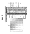
- FIG. 2 is a sectional view taken along line 2-2' of FIG. 1.
- the structure of a conventional input protection circuit that is, the structure of an ESD circuit includes: an N-type well 12 formed in a predetermined region of a P-type semiconductor substrate 10; a heavily doped N-type active guardline 14 formed in the upper surface of the N-type well 12 in order to form an ohmic contact between the N-type well 12 and a metal interconnection (not shown) used to supply power supply voltage (Vcc) thereto; a heavily doped P-type active guardline 16 formed on the edge portion of the semiconductor substrate 10 surrounded by the N -type well 12 in order to lower the contact resistance between the P-type substrate 10 and a metal interconnection (not shown) connected to ground; an N-type source region 18 and an N-type drain region 22 formed in the surface of the semiconductor substrate 10 surrounded by the P-type active guardlines 16 and separated by a predetermined distance; and a gate electrode 20 formed on the upper surface of a gate insulating film (not shown) which is formed on the upper surface of
- the source region 18, the drain region 22 and the gate electrode 20 constitute an NMOS transistor, and the source region 18 as well as the semiconductor substrate 10 are grounded.
- the drain region 22 of the NMOS transistor is connected to an address pad 26 through an interconnection 24 and to an input terminal (not shown) of an internal circuit formed in another region of the semiconductor substrate 10, i.e., a gate electrode (not shown) of a logic circuit.
- the electrons emitted into the semiconductor substrate 10 change the ground potential of the semiconductor substrate 10 to a negative potential (noise). This is called the undershoot phenomenon.
- the undershoot phenomenon leads to a malfunction of the internal circuitry formed in semiconductor substrate 10.
- EP 0 428 067 discloses a semiconductor integrated circuit including a bipolar transistor and an insulated gate transistor, in which the insulated gate transistor is formed in an isolated island. The use of buried and isolated regions within a semiconductor integrated device is also used in the devices described in EP 0 384 396 and JP 61 281 545 A.
- ESD electro-static discharge
- a semiconductor device comprising an NMOS transistor formed in a P-type substrate, having an input/output pad connected to the drain region of the NMOS transistor, and having an electrostatic discharge structure protecting the input/output pad, wherein:
- the electrostatic discharge structure may instead protect an address pad.
- FIG. 1 shows semiconductor memory devices having an address pad and an input/output pad.
- the present invention can be employed in a general semiconductor device as well as the semiconductor memory device.
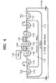
- an ESD structure having an address pad includes: a P-type semiconductor substrate 110; an N-type well 112 formed in a predetermined region of the semiconductor substrate 110; a P-type pocket well 113 formed in a predetermined region of the N-type well 112; and N-type active guardline 114 doped to a concentration higher than that of the N-type well 112 and formed in the surface of the N-type well 112; and a P-type active guardline 116 doped to a concentration higher than that of the P-type pocket well 113 and formed in the upper surface of the P-type pocket well 113.
- the N-type active guardline 114 should be doped at 1.0 x 10 18 /cm 3 or higher in order to form an ohmic contact between the N-type well 112 and an interconnection (not shown), e.g., an aluminium pattern for applying the power supply voltage Vcc to the N-type well 112.
- the P-type active guardline 116 should be doped at 1.0 x 10 18 /cm 3 or higher in order to decrease the contact resistance between the P-type well 113 and an interconnection (not shown), e.g., an aluminium pattern for connecting the P-type well 113 to ground.
- the ESD structure having an address pad further includes: an N-type source region 118 and an N-type drain region 122 which define a channel region formed in the surface of a predetermined region of the P-type pocket well 113; a gate electrode 120 formed on a gate insulating film (not shown) above the channel region between the source region 118 and the drain region 122; and an address pad 126 connected to the drain region 122 through an interconnection 124.
- the ground terminal is connected to the source region 118 as well as the P-type active guardline 116, and the source region 118, the drain region 122 and the gate electrode 120 constitute an NMOS transistor for ESD.
- an NMOS transistor is formed in the P-type pocket well 113 which is completely isolated from the P-type semiconductor substrate 110 by the N-type well 112 surrounding the P-type pocket well 113. Accordingly, even with a negative voltage temporarily applied to the address pad 126, the potential of the semiconductor substrate 110 is stable, i.e., stably grounded.
- a forward bias voltage occurs between the P-type pocket well 112 and the drain region 122 which causes electrons to be emitted from the drain region 122.
- the electrons move to the power supply terminal or the ground terminal through the source region 118, the P-type guardline 116 and the N-type guardline 114, and, since the P-type pocket well 113 is surrounded by the N-type well 112, most of the electrons emitted into the P-type pocket well 113 are rapidly moved to the N-type well 112. Accordingly, the electrons emitted from the drain region 122 remain in the P-type pocket well 113 for an extremely short amount of time so that the potential of the P-type pocket well 113 is prevented from changing. Although all of the electrons emitted into the P-type pocket well 113 cannot be rapidly transmitted to the N-type well 112, the P-type semiconductor substrate 110 keeps a stable ground potential. This is because the P-type semiconductor substrate 110 is completely isolated from the P-type pocket well 113 by the N-type well 112. Accordingly, the internal circuitry (not shown) formed in the P-type semiconductor substrate 110 is protected from noise caused by undershoot.
- FIGS. 5 and 6 are diagrams illustrating an ESD structure having an input/output pad.
- the ESD structure is composed of a pull-up transistor portion formed of PMOS transistors and a pull-down transistor portion formed of NMOS transistors.
- FIG. 5 is a diagram showing a conventional ESD structure
- FIG. 6 is a diagram showing an ESD structure according to the present invention. Portions indicated by the same reference designations as those used in FIGS. 1 and 3 are the same; therefore, a detailed description thereof will be omitted.
- the pull-down transistor portion of FIG. 5 is formed of NMOS transistors, the same problems as those described in FIGS. 1 and 2 occur. In order to solve such problems, the ESD structure described in FIGS. 3 and 4 is selected, thereby to obtain the same effect as that in the first embodiment.
- the present invention can be employed for an ESD structure having an input/output pad in which the pull-up transistor portion and the pull-down transistor portion are both formed of NMOS transistors. That is, in the case that the pull-up transistor portion and the pull-down transistor portion are formed of NMOS transistors, the NMOS transistor of the pull-up transistor portion as well as that for the pull-down transistor portion is formed in the P-type pocket well, thereby to obtain the same effect as that in the first embodiment.
- the NMOS transistors for ESD are formed in the P-type pocket well which is isolated from the semiconductor substrate, to thereby prevent a malfunction of the semiconductor device caused by undershoot.
Applications Claiming Priority (2)
| Application Number | Priority Date | Filing Date | Title |
|---|---|---|---|
| KR9569728 | 1995-12-30 | ||
| KR1019950069728A KR100190008B1 (ko) | 1995-12-30 | 1995-12-30 | 반도체 장치의 정전하 보호 장치 |
Publications (2)
| Publication Number | Publication Date |
|---|---|
| EP0782192A1 EP0782192A1 (en) | 1997-07-02 |
| EP0782192B1 true EP0782192B1 (en) | 2002-07-10 |
Family
ID=19448555
Family Applications (1)
| Application Number | Title | Priority Date | Filing Date |
|---|---|---|---|
| EP96309150A Expired - Lifetime EP0782192B1 (en) | 1995-12-30 | 1996-12-13 | Electrostatic discharge structure of semiconductor device |
Country Status (7)
| Country | Link |
|---|---|
| US (1) | US5760446A (ko) |
| EP (1) | EP0782192B1 (ko) |
| JP (1) | JPH09191080A (ko) |
| KR (1) | KR100190008B1 (ko) |
| CN (1) | CN1135619C (ko) |
| DE (1) | DE69622251T2 (ko) |
| TW (1) | TW329556B (ko) |
Families Citing this family (28)
| Publication number | Priority date | Publication date | Assignee | Title |
|---|---|---|---|---|
| WO1997020348A1 (en) | 1995-11-30 | 1997-06-05 | Micron Technology, Inc. | Structure for esd protection in semiconductor chips |
| US6507074B2 (en) * | 1995-11-30 | 2003-01-14 | Micron Technology, Inc. | Structure for ESD protection in semiconductor chips |
| KR100486223B1 (ko) * | 1997-12-17 | 2005-08-01 | 삼성전자주식회사 | 반도체 장치의 입/출력 패드 |
| US5847431A (en) * | 1997-12-18 | 1998-12-08 | Intel Corporation | Reduced capacitance transistor with electro-static discharge protection structure |
| EP0932202B1 (en) | 1997-12-31 | 2006-09-20 | STMicroelectronics S.r.l. | ESD protection network on semiconductor circuit structures |
| EP0932203B1 (en) * | 1997-12-31 | 2009-02-18 | STMicroelectronics S.r.l. | Method and circuit for improving the performances of an ESD protection on semiconductor circuit structures |
| JP3123984B2 (ja) | 1998-07-31 | 2001-01-15 | 日本電気アイシーマイコンシステム株式会社 | 半導体集積回路装置 |
| WO2000008688A1 (en) * | 1998-08-04 | 2000-02-17 | Koninklijke Philips Electronics N.V. | An integrated circuit provided with esd protection means |
| US6049112A (en) * | 1998-09-14 | 2000-04-11 | Intel Corporation | Reduced capacitance transistor with electro-static discharge protection structure and method for forming the same |
| US6455898B1 (en) * | 1999-03-15 | 2002-09-24 | Macronix International Co., Ltd. | Electrostatic discharge input protection for reducing input resistance |
| US6222237B1 (en) * | 1999-05-21 | 2001-04-24 | United Microelectronics Corp. | Structure of electrostatic discharge protection device |
| TW426973B (en) * | 1999-10-16 | 2001-03-21 | Winbond Electronics Corp | Latch up protection circuit and its method suitable for use in multi power supply integrated circuit |
| US6455902B1 (en) | 2000-12-06 | 2002-09-24 | International Business Machines Corporation | BiCMOS ESD circuit with subcollector/trench-isolated body mosfet for mixed signal analog/digital RF applications |
| US7106568B2 (en) * | 2004-08-27 | 2006-09-12 | United Microelectronics Corp. | Substrate-triggered ESD circuit by using triple-well |
| US7317204B2 (en) * | 2005-01-13 | 2008-01-08 | Samsung Electronics Co., Ltd. | Test structure of semiconductor device |
| CN101281909B (zh) * | 2008-05-28 | 2010-04-21 | 浙江大学 | Nmos管嵌入式双向可控硅静电防护器件 |
| US8378422B2 (en) * | 2009-02-06 | 2013-02-19 | Taiwan Semiconductor Manufacturing Company, Ltd. | Electrostatic discharge protection device comprising a plurality of highly doped areas within a well |
| JP5849670B2 (ja) * | 2011-12-09 | 2016-02-03 | セイコーエプソン株式会社 | 半導体装置 |
| US8853784B2 (en) * | 2012-01-19 | 2014-10-07 | Globalfoundries Singapore Pte. Ltd. | ESD protection circuit |
| CN103378084B (zh) * | 2012-04-13 | 2016-01-20 | 南亚科技股份有限公司 | 存储装置 |
| US20140246725A1 (en) * | 2013-03-04 | 2014-09-04 | Samsung Electronics Co., Ltd. | Integrated Circuit Memory Devices Including Parallel Patterns in Adjacent Regions |
| CN103812483A (zh) * | 2014-01-13 | 2014-05-21 | 智坤(江苏)半导体有限公司 | Cmos射频开关 |
| JP5669119B1 (ja) * | 2014-04-18 | 2015-02-12 | 株式会社パウデック | 半導体素子、電気機器、双方向電界効果トランジスタおよび実装構造体 |
| US9484977B2 (en) * | 2014-05-14 | 2016-11-01 | Dsp Group, Ltd. | RF transformer based TX/RX integrated RF switch |
| CN106158832A (zh) * | 2015-04-01 | 2016-11-23 | 联华电子股份有限公司 | 半导体结构 |
| DE102016115286A1 (de) * | 2016-08-17 | 2018-02-22 | Infineon Technologies Ag | Integrierte Schaltung mit Verstärker-MOSFET |
| US10134722B2 (en) * | 2017-04-12 | 2018-11-20 | Hong Kong Applied Science and Technology Research Institute Company Limited | Embedded PMOS-trigger silicon controlled rectifier (SCR) with suppression rings for electro-static-discharge (ESD) protection |
| US11031462B1 (en) * | 2019-12-23 | 2021-06-08 | Nanya Technology Corporation | Semiconductor structure with improved guard ring structure |
Family Cites Families (5)
| Publication number | Priority date | Publication date | Assignee | Title |
|---|---|---|---|---|
| JPS58165369A (ja) * | 1982-03-26 | 1983-09-30 | Toshiba Corp | 入力保護回路 |
| JPS61281545A (ja) * | 1985-06-06 | 1986-12-11 | Fuji Electric Co Ltd | バイポ−ラ・cmos半導体装置 |
| JPH0685422B2 (ja) * | 1985-11-07 | 1994-10-26 | 三菱電機株式会社 | 半導体集積回路 |
| JP2509690B2 (ja) * | 1989-02-20 | 1996-06-26 | 株式会社東芝 | 半導体装置 |
| JPH0744231B2 (ja) * | 1989-11-10 | 1995-05-15 | 株式会社東芝 | 半導体集積回路およびその製造方法 |
-
1995
- 1995-12-30 KR KR1019950069728A patent/KR100190008B1/ko not_active IP Right Cessation
-
1996
- 1996-12-13 DE DE69622251T patent/DE69622251T2/de not_active Expired - Lifetime
- 1996-12-13 EP EP96309150A patent/EP0782192B1/en not_active Expired - Lifetime
- 1996-12-16 JP JP8335781A patent/JPH09191080A/ja active Pending
- 1996-12-24 US US08/774,936 patent/US5760446A/en not_active Expired - Lifetime
- 1996-12-24 TW TW085116022A patent/TW329556B/zh not_active IP Right Cessation
- 1996-12-27 CN CNB96116722XA patent/CN1135619C/zh not_active Expired - Lifetime
Non-Patent Citations (1)
| Title |
|---|
| Principles of CMOS VLSI Design by Weste & Eshraghian pub. Addison-Wesley 1985, pgs. 58-60 * |
Also Published As
| Publication number | Publication date |
|---|---|
| CN1135619C (zh) | 2004-01-21 |
| KR970053883A (ko) | 1997-07-31 |
| EP0782192A1 (en) | 1997-07-02 |
| TW329556B (en) | 1998-04-11 |
| KR100190008B1 (ko) | 1999-06-01 |
| JPH09191080A (ja) | 1997-07-22 |
| DE69622251T2 (de) | 2003-03-13 |
| DE69622251D1 (de) | 2002-08-14 |
| CN1154578A (zh) | 1997-07-16 |
| US5760446A (en) | 1998-06-02 |
Similar Documents
| Publication | Publication Date | Title |
|---|---|---|
| EP0782192B1 (en) | Electrostatic discharge structure of semiconductor device | |
| US5615073A (en) | Electrostatic discharge protection apparatus | |
| US7485930B2 (en) | Method for four direction low capacitance ESD protection | |
| KR0164908B1 (ko) | 보호 트랜지스터를 가진 반도체 장치 | |
| US5218222A (en) | Output ESD protection circuit | |
| KR930010827B1 (ko) | 반도체장치 | |
| KR100417093B1 (ko) | 반도체장치 | |
| JPH0729972A (ja) | 半導体装置 | |
| US5181092A (en) | Input protection resistor used in input protection circuit | |
| EP0415255B2 (en) | Protection circuit for use in semiconductor integrated circuit device | |
| US5898193A (en) | Electrostatic discharge protecting circuit formed in a minimized area | |
| US5706156A (en) | Semiconductor device having an ESD protective circuitry | |
| JP3320872B2 (ja) | Cmos集積回路装置 | |
| US6218881B1 (en) | Semiconductor integrated circuit device | |
| KR100301538B1 (ko) | 반도체장치 | |
| KR100371246B1 (ko) | 반도체장치의보호회로 | |
| JP3149999B2 (ja) | 半導体入出力保護装置 | |
| US6084272A (en) | Electrostatic discharge protective circuit for semiconductor device | |
| KR0131373B1 (ko) | 반도체 소자의 데이터 출력버퍼 | |
| JPH044755B2 (ko) | ||
| KR100270949B1 (ko) | 극성에 상관없이 내부 회로를 보호하기 위하여 전원 공급 단자들 사이에 적용한 정전기 방지 회로 | |
| KR100379330B1 (ko) | 정전적방전(esd)구조 | |
| JPH1168043A (ja) | Esd保護回路 | |
| US5432369A (en) | Input/output protection circuit | |
| KR100494143B1 (ko) | 반도체장치의 필드트랜지스터 구조 |
Legal Events
| Date | Code | Title | Description |
|---|---|---|---|
| PUAI | Public reference made under article 153(3) epc to a published international application that has entered the european phase |
Free format text: ORIGINAL CODE: 0009012 |
|
| AK | Designated contracting states |
Kind code of ref document: A1 Designated state(s): DE FR GB |
|
| 17P | Request for examination filed |
Effective date: 19971210 |
|
| 17Q | First examination report despatched |
Effective date: 19990616 |
|
| GRAG | Despatch of communication of intention to grant |
Free format text: ORIGINAL CODE: EPIDOS AGRA |
|
| GRAG | Despatch of communication of intention to grant |
Free format text: ORIGINAL CODE: EPIDOS AGRA |
|
| GRAH | Despatch of communication of intention to grant a patent |
Free format text: ORIGINAL CODE: EPIDOS IGRA |
|
| GRAH | Despatch of communication of intention to grant a patent |
Free format text: ORIGINAL CODE: EPIDOS IGRA |
|
| GRAA | (expected) grant |
Free format text: ORIGINAL CODE: 0009210 |
|
| AK | Designated contracting states |
Kind code of ref document: B1 Designated state(s): DE FR GB |
|
| REF | Corresponds to: |
Ref document number: 69622251 Country of ref document: DE Date of ref document: 20020814 |
|
| ET | Fr: translation filed | ||
| PLBE | No opposition filed within time limit |
Free format text: ORIGINAL CODE: 0009261 |
|
| STAA | Information on the status of an ep patent application or granted ep patent |
Free format text: STATUS: NO OPPOSITION FILED WITHIN TIME LIMIT |
|
| 26N | No opposition filed |
Effective date: 20030411 |
|
| REG | Reference to a national code |
Ref country code: FR Ref legal event code: PLFP Year of fee payment: 20 |
|
| PGFP | Annual fee paid to national office [announced via postgrant information from national office to epo] |
Ref country code: GB Payment date: 20151125 Year of fee payment: 20 Ref country code: DE Payment date: 20151119 Year of fee payment: 20 |
|
| PGFP | Annual fee paid to national office [announced via postgrant information from national office to epo] |
Ref country code: FR Payment date: 20151123 Year of fee payment: 20 |
|
| REG | Reference to a national code |
Ref country code: DE Ref legal event code: R071 Ref document number: 69622251 Country of ref document: DE |
|
| REG | Reference to a national code |
Ref country code: GB Ref legal event code: PE20 Expiry date: 20161212 |
|
| PG25 | Lapsed in a contracting state [announced via postgrant information from national office to epo] |
Ref country code: GB Free format text: LAPSE BECAUSE OF EXPIRATION OF PROTECTION Effective date: 20161212 |