EP0751571A2 - Mehrschicht-Hybridschaltkreis - Google Patents
Mehrschicht-Hybridschaltkreis Download PDFInfo
- Publication number
- EP0751571A2 EP0751571A2 EP96202397A EP96202397A EP0751571A2 EP 0751571 A2 EP0751571 A2 EP 0751571A2 EP 96202397 A EP96202397 A EP 96202397A EP 96202397 A EP96202397 A EP 96202397A EP 0751571 A2 EP0751571 A2 EP 0751571A2
- Authority
- EP
- European Patent Office
- Prior art keywords
- conductor
- coils
- dielectric
- layer
- conductive
- Prior art date
- Legal status (The legal status is an assumption and is not a legal conclusion. Google has not performed a legal analysis and makes no representation as to the accuracy of the status listed.)
- Withdrawn
Links
Images







Classifications
-
- H—ELECTRICITY
- H03—ELECTRONIC CIRCUITRY
- H03H—IMPEDANCE NETWORKS, e.g. RESONANT CIRCUITS; RESONATORS
- H03H7/00—Multiple-port networks comprising only passive electrical elements as network components
- H03H7/01—Frequency selective two-port networks
- H03H7/09—Filters comprising mutual inductance
-
- H—ELECTRICITY
- H03—ELECTRONIC CIRCUITRY
- H03H—IMPEDANCE NETWORKS, e.g. RESONANT CIRCUITS; RESONATORS
- H03H7/00—Multiple-port networks comprising only passive electrical elements as network components
- H03H7/01—Frequency selective two-port networks
- H03H7/17—Structural details of sub-circuits of frequency selective networks
- H03H7/1708—Comprising bridging elements, i.e. elements in a series path without own reference to ground and spanning branching nodes of another series path
-
- H—ELECTRICITY
- H03—ELECTRONIC CIRCUITRY
- H03H—IMPEDANCE NETWORKS, e.g. RESONANT CIRCUITS; RESONATORS
- H03H7/00—Multiple-port networks comprising only passive electrical elements as network components
- H03H7/01—Frequency selective two-port networks
- H03H7/17—Structural details of sub-circuits of frequency selective networks
- H03H7/1716—Comprising foot-point elements
- H03H7/1725—Element to ground being common to different shunt paths, i.e. Y-structure
-
- H—ELECTRICITY
- H03—ELECTRONIC CIRCUITRY
- H03H—IMPEDANCE NETWORKS, e.g. RESONANT CIRCUITS; RESONATORS
- H03H7/00—Multiple-port networks comprising only passive electrical elements as network components
- H03H7/01—Frequency selective two-port networks
- H03H7/17—Structural details of sub-circuits of frequency selective networks
- H03H7/1741—Comprising typical LC combinations, irrespective of presence and location of additional resistors
- H03H7/1758—Series LC in shunt or branch path
-
- H—ELECTRICITY
- H03—ELECTRONIC CIRCUITRY
- H03H—IMPEDANCE NETWORKS, e.g. RESONANT CIRCUITS; RESONATORS
- H03H7/00—Multiple-port networks comprising only passive electrical elements as network components
- H03H7/01—Frequency selective two-port networks
- H03H7/17—Structural details of sub-circuits of frequency selective networks
- H03H7/1741—Comprising typical LC combinations, irrespective of presence and location of additional resistors
- H03H7/1766—Parallel LC in series path
-
- H—ELECTRICITY
- H05—ELECTRIC TECHNIQUES NOT OTHERWISE PROVIDED FOR
- H05K—PRINTED CIRCUITS; CASINGS OR CONSTRUCTIONAL DETAILS OF ELECTRIC APPARATUS; MANUFACTURE OF ASSEMBLAGES OF ELECTRICAL COMPONENTS
- H05K1/00—Printed circuits
- H05K1/16—Printed circuits incorporating printed electric components, e.g. printed resistors, capacitors or inductors
-
- H—ELECTRICITY
- H10—SEMICONDUCTOR DEVICES; ELECTRIC SOLID-STATE DEVICES NOT OTHERWISE PROVIDED FOR
- H10D—INORGANIC ELECTRIC SEMICONDUCTOR DEVICES
- H10D86/00—Integrated devices formed in or on insulating or conducting substrates, e.g. formed in silicon-on-insulator [SOI] substrates or on stainless steel or glass substrates
- H10D86/80—Integrated devices formed in or on insulating or conducting substrates, e.g. formed in silicon-on-insulator [SOI] substrates or on stainless steel or glass substrates characterised by multiple passive components, e.g. resistors, capacitors or inductors
- H10D86/85—Integrated devices formed in or on insulating or conducting substrates, e.g. formed in silicon-on-insulator [SOI] substrates or on stainless steel or glass substrates characterised by multiple passive components, e.g. resistors, capacitors or inductors characterised by only passive components
-
- H—ELECTRICITY
- H03—ELECTRONIC CIRCUITRY
- H03H—IMPEDANCE NETWORKS, e.g. RESONANT CIRCUITS; RESONATORS
- H03H1/00—Constructional details of impedance networks whose electrical mode of operation is not specified or applicable to more than one type of network
- H03H2001/0021—Constructional details
- H03H2001/0085—Multilayer, e.g. LTCC, HTCC, green sheets
Definitions
- the present invention relates to an improvement of a multilayer hybrid circuit which has a laminated printed circuit board including, at least, inductors, capacitors, and resistors in the printed circuit board itself.
- the USP 4,322,698 provides one solution for high density mounting, and discloses a multilayer hybrid circuit which has a laminated printed circuit board which includes an inductor, a capacitor and/or a resistor. Since those components are produced in a board (not on the surface of the board), the size of the system can be miniturized, and the high density mounting has become possible.
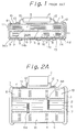
- Fig.1 shows such prior multilayer hybrid circuit.
- a laminated body 1A has a plurality of dielectric laminated layers 3 and a plurality of conductive films 4 so that those conductive films 4 and those dielectric layers 3 compose a plurality of capacitors 5.
- inductors 16 having an internal conductor 14 and a ferrite layer 15 are also provided.
- an U-shaped conductive pattern 14a is printed, next a ferrite pattern which is dielectric is deposited so that a window is kept at the one end of said U-shaped pattern 14a.
- another U-shaped conductive pattern 14b is deposited on the ferrite pattern so that end of the pattern 14a at the window of the ferrite pattern is connected to the end of the second pattern 14b.
- one turn coil is produced by a pair of U-shaped conductive patterns 14a and 14b.
- an inductor with a plurality of turns 14a and 14b is produced.
- another inductor having U-shaped patterns 14c and 14d is produced.
- a glass layer 6 is attached on at least one surface of the laminated body 1A, and a resistor network 9 which has a resistor layer 8 and a conductive layer 7 is attached on said glass layer 6.
- a printed wiring pattern 10 is deposited on at least one surface of the laminated body 1A, and a plurality of side terminals 11 for external connection are deposited on the sides of the laminated body 1A.
- the conductive pattern 10 is used for mounting an electronic component 2 (for instance an integrated circuit, or a transistor) on the laminated body 1A.
- the laminated boyd 1A is produced through thick film printing process, and sintering process.
- An external electronic component 2 is soldered on the conductive pattern 10 by soldering a terminal wire 12 of the component 2 to the conductive pattern 10 by the solder 13.
- a prior multilayer hybrid circuit of Fig.1 has the disadvantage that wiring between a surface component, and a capacitor, an inductor, or a resistor is effected by using a surface printed conductive pattern 10 and a side terminal 11 deposited on the surface of the laminated body.
- the wiring pattern 10 must also be complicated.
- the area or the size of the board for the wiring pattern must be large, and sometimes that area required for wiring is larger than the area for mounting internal passive components.
- a large number of side terminals 11 must be provided, and the insulation between the side terminals 11 is difficult when the side terminals 11 are so densed.
- the present applicant proposed the US filing serial number 464,453 and EP filing serial number 90 400 092. That proposal has not only a capacitor layer, an inductor layer, and a resistor layer, but also an inner wiring layer for connection between inner components.
- the inner wiring layer has a dielectric layer, a conductive pattern deposited on the dielectric layer, and a conductive through hole for connecting electrically conductive patterns on different dielectric layers.
- the present invention is the improvement of said previous invention.
- the present invention improves in particular that a through hole is improved in a specific structure with high operational reliability.
- Another disadvantage of a prior multilayer hybrid circuit is that it is difficult to provide an inductor with high inductance.
- the inductance depends upon the number of windings of a coil, the number of the windings must be large when the inductance is high, and that large number of windings results in the increase of the thickness of the hybrid circuit. Therefore, a thin structure having large inductance has been desired.
- a multilayer hybrid circuit comprising an essentially flat-shaped laminated body which includes at least one selected from a capacitor, an inductor, a resistor, and an inner wiring portion which couples said capacitor, said inductor and/or said resistor with each other, and a plurality of side terminals provided on side walls of said laminated body for external connection of said capacitor, said inductor, and said resistor; said capacitor including a dielectric layer and conductive layers on said dielectric layer; said inductor including a dielectric magnetic layer and a plurality of conductive wire layers composing a coil by sandwiching said magnetic layer between conductive wire layers; said resistor including a dielectric layer and a resistor layer deposited on said dielectric layer together with a conductive layer as a lead line; said inner wiring portion having at least one dielectric layer, a conductive layer deposited on said dielectric layer according to desired wiring pattern; a coupling conductor penetrating said dielectric layers of at least one of said capacitor, said inductor, said
- At least one of said inductors has a plurality of coils having an essentially common axis wound in opposite direction and connected in series on the plane where one ends of each coils reside so that flux by each coils is in the same direction, and wherein conductive wire layer composing a part of each coils are deposited on the same dielectric magnetic layers.
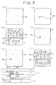
- Fig.2A shows a cross section of a multilayer hybrid circuit according to the present invention
- Fig.2B is a perspective view of the same, in which 1A is an inductor, 2 is a capacitor, 1B is another inductor, and 3 is a side terminal which is coupled with a conductor 4 of the inductors 1A and/or 1B, and the electrode conductor 5 of the capacitor 2.
- the capacitor 2 is sandwiched between the inductors 1A and 1B in order to prevent crosstalk between the inductors in case of a large number of inner elements like an LC filter as shown in Fig.4.
- a resistor and/or an inner wiring portion may also be laminated.
- a resistor layer has a dielectric layer and a resistor layer deposited on said dielectric layer together with a conductive layer as a lead line.
- An inner wiring portion has at least one dielectric layer, a conductive layer deposited on said dielectric layer according desired wiring pattern for coupling capacitors, inductors, or resistors mounted on the present multilayer hybrid circuit.
- an external electronic component like an integrated circuit, 2 is mounted on the laminated body of the hybrid circuit.
- Said component is coupled with a side terminal or inner elements through a conductive pattern on the hybrid circuit, or an inner coupling conductor.
- a coupling conductor is also provided perpendicular to the dielectric layers so that components and/or conductive patterns on different dielectric layers are electrically connected.
- the multilayer hybrid circuit of Fig. 2A-2B is produced as follows.
- An inductor 1A is first produced so that a ferrite layer in the paste form by a binder, and an essentially U-shaped conductive layer are laminated alternately through printing process.
- An end of the U-shaped conductor 4 on one surface of the ferrite paste layer is coupled with another U-shaped conductor on the surface of another ferrite paste layer so that two U-shaped conductors provide a one turn coil conductor.
- a capacitor 2 is then formed on the inductor 1A.
- the capacitor 2 is produced by laminating a dielectric layer 7 and an electrode conductor 5 alternately through printing process. Further, another inductor 1B is formed on said capacitor 2.
- the coupling conductors 8A and 8B are produced simultaneously to make the inductors 1A and 1B, and the capacitor 2.
- the laminated body having inductors 1A and 1B, and a capacitor 2, together with the coupling conductors is then sintered. Then, a plurality of side terminals 3 are formed through printing process and sintering process.
- a coupling conductor 8A and/or 8B for coupling elements on different planes is produced.
- the coupling conductor 8A connects the inductor 1A to the capacitor 2, and the coupling conductor 8B connects the capacitor 2 to the inductor 1B. Only two coupling conductors 8A and 8B are shown for the simplicity of the drawing, and it should be noted of course that other coupling conductors may be mounted.
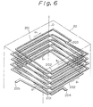
- Fig.3 shows the producing steps of a coupling conductor.
- the coupling conductor 8B for connecting the conductor 4 of the inductor 1B to the capacitor 2 is described.
- the dielectric layer 7a which is made of dielectric powder and binder is placed, on a substrate as shown in Fig.3(a).
- a conductor pattern 5a which relates to a pattern of a capacitor electrode is formed on said layer 7a as shown in Fig.3(b).
- Fig.3(b) it is supposed that the conductor X is to be connected to the inductor 1B, and the conductor X has the projection 8a, which is to be coupled with a coupling conductor.
- the conductive paste for the conductive layer 5a and 8a is made of mixture of metal powder including Ag, Ag-Pd, Cu, Ni and Pd, and binder.
- a dielectric layer 7b is deposited on the pattern of Fig.3(b), with a window at the position of the conductive projection 8a, as shown in Fig.3(c).
- Fig.3(j) shows the laminated cross section.
- a conductive chip 8b is provided so that the chip 8b is coupled with the projection 8a, and partly occupies the surface of the dielectric layer 7b (see cross section of Fig.3(j)) through the window on the dielectric layer 7b. It should be noted that the conductive chip 8b is essentially S-shaped.
- a dielectric layer 7c is provided on the dielectric 7b so that a window opens on a part of the conductor 8b at the opposite end of the conductor 8a.
- the window in Fig.3(e) is shifted in view of the window of Fig.3(c) by the length d so that a coupling conductor extends perpendicular to the dielectric layers in a zigzag manner, or in S-shaped manner.
- a conductive pattern 5b which is a counter electrode for the conductive pattern 5a of a capacitor is provided on the dielectric layer 7c.
- the shape of the pattern 5b differs from that of the pattern 5a in the portions which are coupled with side terminals 3.
- a conductor chip 8c which is coupled with the conductor chip 8b is provided so that the end of the chip 8c is on the dielectric layer 7c.
- the conductive chip 8c does not couple with the conductor Y, which is a counter electrode of the electrode X for providing a capacitor.
- the thickness of the dielectric layers between the conductive patterns 5a and 5b in Figs.3(b) and 3(f) is 20-150 ⁇ m, and it should be appreciated that each printing thickness is 5-10 ⁇ m, and therefore a plurality of printing processes are carried out to obtain said thickness (20-150 ⁇ m) because single printing process with enough thickness is impossible due to rapid dry feature of the dielectric paste.
- the dielectric layer 7d is provided on the pattern of Fig.3(f) with a window which opens a part of the conductive chip 8c.
- a conductor chip 8d which is coupled with the end of the conductor chip 8c is deposited so that the end of the chip 8d is on the dielectric layer 7d.
- a dielectric layer 7e is deposited with a window so that a part of the conductor chip 8d at the opposite end of the coupling portion with the conductor chip 8c is not covered with the dielectric layer 7e.
- the above processes are repeated by the necessary times to obtain a coupling conductor 8B.
- the coupling conductor 8A in the inductor layer 1B is produced through similar processes.
- a coupling conductor 8B thus produced is in a zigzag shape, or a repeat of essentially S-shape as shown in Fig.5A.
- a coupling conductor is used for coupling inner elements, including an inductor, a capacitor, and/or a resistor with each other, and/or an external element, so that no side terminal 3 is used for the inner element coupling.
- the use of a coupling conductor allows a complicated circuit in the present multilayer hybrid circuit. For instance, a filter circuit shown in Fig.4 having 17 coupling points (shown by a circle in the figure) may be mounted in a hybrid circuit of 5.0 mm x 5.0 mm x 2.8 mm size having only 12 side terminals.
- a coupling conductor extends to the surface of the hybrid circuit when an external element mounted on the hybrid circuit is coupled through the coupling conductor.
- Figs.5B and 5C show for the explanation of the effect of the present coupling conductor. If a coupling conductor is implemented by a through hole filled with a conductor in a conventional manner as shown in Figs.5B and 5C, a small contraction or expansion in sintering process between a conductor in a through hole, and a dielectric layer or a ferrite layer would cause trouble.
- a coupling conductor itself is in a laminated structure of S-shaped conductor chips and dielectric layers (or ferrite layers).
- Each conductive chip of the coupling conductor is very thin, and is provided between dielectric or ferrite layers.
- inductance is proportional to number of windings, so when large inductance is requested, number of turns is large according to the necessary inductance.
- the increase of number of turns causes the increase of the thickness of the circuit. As the thickness must be smaller than a requested value, the number of turns is restricted, and the necessary inductance is sometimes not obtained.
- the basic idea of the present invention to solve the above problem and provide large inductance is to provide a plurality of windings each connected in series so that inductance is increased.
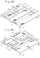
- Fig.6 shows an enlarged perspective view of a coil according to the present invention.
- 20 is a ferromagnetic body
- 201 and 202 are coils
- 203 is a conductive coupling chip of two coils 201 and 202
- 204 and 205 are terminals of a series connected coil.
- Each coil 201 and 202 is spiral or solinoid along the coil axis O, and the coil axis of the first coil 201 resides within the other coil 202.
- the winding direction a 1 of the first coil 201 is opposite to the winding direction b 1 of the second coil 202.
- the coil 201 is wound in clockwise direction
- the other coil 202 is wound in anti-clockwise direction.
- One end of the coils 201 and 202 is coupled with each other by using a coupling conductor 203.
- the current direction in the coil 201 is the same as that in the coil 202, and the coil 201 and coil 202 provide the flux in the same direction.
- the other ends 204 and 205 of the coils 201 and 202 are provided at one end of the series connected coil, and are connected to a side terminal, or inner components, or a coupling conductor.
- the inductance of the series connected coil is four times as large as the inductance of each coil 201 or 202, provided that the number of turns of the coil 201 is the same as that of the coil 202.
- the coils 201 and 202 are solenoids with the axis O, and the axis O resides in both the solenoid plane. Therefore, the size of the series connected coils 201 and 202 is almost the same as the size of one coil 201 or 202. So, the size of the coil is small as compared with that of the inductance, and large inductance is obtained in a thin hybrid structure.
- the coils 201 and 202 are wound in opposite direction, and the coupling conductor 203 connects two coils in series. Therefore, no through hole conductor is used for connecting two coils in series.
- Fig.7 shows the embodiment that three coils 200, 201 and 202 are connected in series. Those coils 200, 201 and 202 are solenoids with the axis O, which resides commonly in all the coils.
- the winding direction a 0 of the first coil 200 is opposite to that b 1 of the second coil 201, and the direction b 1 is opposite to the direction a 1 of the third coil 202.
- the present multilayer hybrid circuit is produced through printing process, photolithoetching process, sputtering process, evaporation process, and/or plating process.
- a thick film printing process is described.
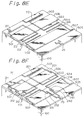
- a pair of elongated ferromagnetic layers 501 and 502 in stripe form are printed on a substrate 100 as shown in Fig.8A.
- the substrate 100 is supposed to be a component which has been already laminated.
- Those magnetic layers 501 and 502 are produced through screen printing process of ferromagnetic paste which is the mixture of ferrite powder, binder and solvent. It should be noted that a ferrite layer is dielectric.
- conductor chips or lines 212, 222, 231 and 241 are printed on the magnetic layers 501 and 502, and the substrate. Those conductor chips function as a part of coils, and terminals of those coils.
- the ferromagnetic layers 503 through 505 are printed so that the portions which are not covered with the first magnetic layers 501 and 502 are covered with the second magnetic layers 503, 504 and 505.
- the ends of the conductive chips 212, 222, 231 and 241 are not covered with the second magnetic layers.
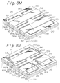
- conductive chips 212, 222, 231 and 241 are printed on the magnetic layer 504 so that those conductive chips 212, 222, 231, and 241 are connected to those which are printed in Fig.8B.
- the conductive chip 211 and 221 are printed on the magnetic layer 503, and the conductive chip 25 is printed on the magnetic layer 505.
- the ferromagnetic layers 506 and 507 are printed so that the spacing between the layers 503 and 504, and the spacing between the layers 504 and 505 are filled.
- the conductor chips 211 and 221 are provided on the magnetic layers 503 and 506 so that those chips 211 and 221 are connected to those which are printed in Fig.8D.
- the conductive chips 212 and 222 are printed on the magnetic layers 504 and 506 so that those conductive chips 212 and 222 are connected to those which are printed in Fig.8D.
- the conductive chips 231 and 241 are printed on the magnetic layers 504 and 507 so that those conductive chips 231 and 241 are connected to those which are printed in Fig.8D.
- the conductive chips 232 and 242 are provided on the magnetic layers 505 and 507 so that those conductor chips 232 and 242 are connected to the conductor 25 on the magnetic layer 505.
- the conductor chips 211 and 212, 221 and 222, 231 and 232, and 241 and 242 are provided so that the former of each pair goes in opposite direction of the latter.
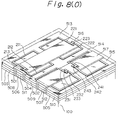
- the conductor chips (211,212) through (241, 242), and the ferromagnetic layers are printed according to the number of turns of the coils.
- the numerals 508 through 517 in those figures are ferromagnetic layers.
- the coupling chips 213, 223, 233 and 243 connects the ends of the coils (221, 212), (221, 222), (231, 232), and (241, 242), respectively. Then, four coils each of which has two serially connected coils are obtained.
- an inductor according to the present invention has a plurality of series connected coils so that large inductance is obtained in thin structure.
- a plurality of coils are provided around the common axis, the total thickness of the coils is almost the same as a single coil, and therefore, the total size of an inductor is almost the same as that of a single coil.
- the coupling chip for connecting the ends of two coils resides on a single plane, and no penetrating conductor is used for the connection of the two coils.
Landscapes
- Engineering & Computer Science (AREA)
- Microelectronics & Electronic Packaging (AREA)
- Coils Or Transformers For Communication (AREA)
- Production Of Multi-Layered Print Wiring Board (AREA)
Applications Claiming Priority (7)
| Application Number | Priority Date | Filing Date | Title |
|---|---|---|---|
| JP326866/89 | 1989-12-15 | ||
| JP32686689A JP3166158B2 (ja) | 1989-12-15 | 1989-12-15 | 積層回路部品の構造 |
| JP38768/90 | 1990-02-20 | ||
| JP2038768A JP3048593B2 (ja) | 1990-02-20 | 1990-02-20 | 混成集積回路部品 |
| JP294424/90 | 1990-10-31 | ||
| JP29442490A JP2971124B2 (ja) | 1990-10-31 | 1990-10-31 | 電子部品 |
| EP90403576A EP0433176B1 (de) | 1989-12-15 | 1990-12-13 | Mehrschicht-Hybridschaltkreis |
Related Parent Applications (2)
| Application Number | Title | Priority Date | Filing Date |
|---|---|---|---|
| EP90403576.3 Division | 1990-12-13 | ||
| EP90403576A Division EP0433176B1 (de) | 1989-12-15 | 1990-12-13 | Mehrschicht-Hybridschaltkreis |
Publications (2)
| Publication Number | Publication Date |
|---|---|
| EP0751571A2 true EP0751571A2 (de) | 1997-01-02 |
| EP0751571A3 EP0751571A3 (de) | 1997-01-08 |
Family
ID=27289937
Family Applications (2)
| Application Number | Title | Priority Date | Filing Date |
|---|---|---|---|
| EP96202397A Withdrawn EP0751571A3 (de) | 1989-12-15 | 1990-12-13 | Mehrschicht-Hybridschaltkreis |
| EP90403576A Expired - Lifetime EP0433176B1 (de) | 1989-12-15 | 1990-12-13 | Mehrschicht-Hybridschaltkreis |
Family Applications After (1)
| Application Number | Title | Priority Date | Filing Date |
|---|---|---|---|
| EP90403576A Expired - Lifetime EP0433176B1 (de) | 1989-12-15 | 1990-12-13 | Mehrschicht-Hybridschaltkreis |
Country Status (4)
| Country | Link |
|---|---|
| US (1) | US5225969A (de) |
| EP (2) | EP0751571A3 (de) |
| DE (1) | DE69033993T2 (de) |
| MY (1) | MY105486A (de) |
Cited By (3)
| Publication number | Priority date | Publication date | Assignee | Title |
|---|---|---|---|---|
| US5889445A (en) * | 1997-07-22 | 1999-03-30 | Avx Corporation | Multilayer ceramic RC device |
| US6525628B1 (en) | 1999-06-18 | 2003-02-25 | Avx Corporation | Surface mount RC array with narrow tab portions on each of the electrode plates |
| CN101778539B (zh) * | 2009-12-23 | 2011-11-09 | 深南电路有限公司 | 一种pcb加工工艺方法 |
Families Citing this family (52)
| Publication number | Priority date | Publication date | Assignee | Title |
|---|---|---|---|---|
| SG48955A1 (en) * | 1992-07-27 | 1998-05-18 | Murata Manufacturing Co | Multilayer electronic component method of manufacturing the same and method of measuring characteristics thereof |
| US5635669A (en) * | 1992-07-27 | 1997-06-03 | Murata Manufacturing Co., Ltd. | Multilayer electronic component |
| DE4340594C2 (de) * | 1992-12-01 | 1998-04-09 | Murata Manufacturing Co | Verfahren zur Herstellung und zum Einstellen der Charakteristik eines oberflächenmontierbaren chipförmigen LC-Filters |
| US5910755A (en) * | 1993-03-19 | 1999-06-08 | Fujitsu Limited | Laminate circuit board with selectable connections between wiring layers |
| CA2092371C (en) * | 1993-03-24 | 1999-06-29 | Boris L. Livshits | Integrated circuit packaging |
| JPH0722243A (ja) * | 1993-07-02 | 1995-01-24 | Murata Mfg Co Ltd | インダクタアレイ |
| JP3461204B2 (ja) * | 1993-09-14 | 2003-10-27 | 株式会社東芝 | マルチチップモジュール |
| US5610565A (en) * | 1994-02-02 | 1997-03-11 | Murata Manufacturing Co., Ltd. | Composite LC device with a ground electrode not formed on the inductor parts |
| JPH07326544A (ja) * | 1994-05-31 | 1995-12-12 | Matsushita Electric Ind Co Ltd | 多層回路基板で形成する可変キャパシタ |
| US5635892A (en) * | 1994-12-06 | 1997-06-03 | Lucent Technologies Inc. | High Q integrated inductor |
| US5545916A (en) * | 1994-12-06 | 1996-08-13 | At&T Corp. | High Q integrated inductor |
| US5559360A (en) * | 1994-12-19 | 1996-09-24 | Lucent Technologies Inc. | Inductor for high frequency circuits |
| US5849355A (en) * | 1996-09-18 | 1998-12-15 | Alliedsignal Inc. | Electroless copper plating |
| WO1997012440A1 (en) * | 1995-09-25 | 1997-04-03 | Alliedsignal Inc. | Planar electronic network |
| TW362222B (en) * | 1995-11-27 | 1999-06-21 | Matsushita Electric Industrial Co Ltd | Coiled component and its production method |
| DE19639947A1 (de) * | 1996-09-27 | 1998-04-16 | Siemens Matsushita Components | Passives Netzwerk in Chip-Bauform |
| US6405031B1 (en) | 1997-02-28 | 2002-06-11 | Dieceland Technologies Corp. | Wireless telephone system, telephone and method |
| US6061580A (en) * | 1997-02-28 | 2000-05-09 | Randice-Lisa Altschul | Disposable wireless telephone and method for call-out only |
| US5965848A (en) * | 1997-07-22 | 1999-10-12 | Randice-Lisa Altschul | Disposable portable electronic devices and method of making |
| US6094112A (en) * | 1997-10-15 | 2000-07-25 | Avx Corporation | Surface mount filter device |
| US5983094A (en) * | 1997-10-27 | 1999-11-09 | Randice-Lisa Altschul | Wireless telephone with credited airtime and method |
| US6054914A (en) * | 1998-07-06 | 2000-04-25 | Midcom, Inc. | Multi-layer transformer having electrical connection in a magnetic core |
| US6021050A (en) * | 1998-12-02 | 2000-02-01 | Bourns, Inc. | Printed circuit boards with integrated passive components and method for making same |
| TW496775B (en) | 1999-03-15 | 2002-08-01 | Aviva Bioscience Corp | Individually addressable micro-electromagnetic unit array chips |
| CN1185492C (zh) | 1999-03-15 | 2005-01-19 | 清华大学 | 可单点选通式微电磁单元阵列芯片、电磁生物芯片及应用 |
| US6198374B1 (en) | 1999-04-01 | 2001-03-06 | Midcom, Inc. | Multi-layer transformer apparatus and method |
| JP2003188047A (ja) * | 2001-12-14 | 2003-07-04 | Mitsubishi Electric Corp | Dcブロック回路および通信装置 |
| JP3941508B2 (ja) * | 2001-02-19 | 2007-07-04 | 株式会社村田製作所 | 積層型インピーダンス素子 |
| US6617526B2 (en) * | 2001-04-23 | 2003-09-09 | Lockheed Martin Corporation | UHF ground interconnects |
| US6963493B2 (en) * | 2001-11-08 | 2005-11-08 | Avx Corporation | Multilayer electronic devices with via components |
| US6922128B2 (en) * | 2002-06-18 | 2005-07-26 | Nokia Corporation | Method for forming a spiral inductor |
| JP4217438B2 (ja) * | 2002-07-26 | 2009-02-04 | Fdk株式会社 | マイクロコンバータ |
| US20040070479A1 (en) * | 2002-10-10 | 2004-04-15 | Yutaka Doi | Via-less electronic structures and methods |
| US7319599B2 (en) * | 2003-10-01 | 2008-01-15 | Matsushita Electric Industrial Co., Ltd. | Module incorporating a capacitor, method for manufacturing the same, and capacitor used therefor |
| JP4120562B2 (ja) * | 2003-10-31 | 2008-07-16 | 沖電気工業株式会社 | 受動素子チップ、高集積モジュール、受動素子チップの製造方法、及び高集積モジュールの製造方法。 |
| US7262139B2 (en) * | 2004-06-02 | 2007-08-28 | Avx Israel, Ltd. | Method suitable for batch ion etching of copper |
| US7253522B2 (en) * | 2004-06-02 | 2007-08-07 | Avx Israel, Ltd. | Integrated capacitor for RF applications with Ta adhesion layer |
| CN102185474B (zh) * | 2005-10-28 | 2013-09-18 | 日立金属株式会社 | Dc-dc转换器 |
| US7613009B2 (en) * | 2006-03-15 | 2009-11-03 | Tdk Corporation | Electrical transition for an RF component |
| US7948078B2 (en) * | 2006-07-25 | 2011-05-24 | Rohm Co., Ltd. | Semiconductor device |
| US7742276B2 (en) * | 2007-03-30 | 2010-06-22 | Industrial Technology Research Institute | Wiring structure of laminated capacitors |
| US8415777B2 (en) * | 2008-02-29 | 2013-04-09 | Broadcom Corporation | Integrated circuit with millimeter wave and inductive coupling and methods for use therewith |
| KR101018554B1 (ko) * | 2009-05-15 | 2011-03-03 | (주)디지털초음파 | 나선형 코일 제조방법과 그 나선형 코일 및 이를 구비한 전자기음향변환기 |
| USD680545S1 (en) * | 2011-11-15 | 2013-04-23 | Connectblue Ab | Module |
| USD692896S1 (en) * | 2011-11-15 | 2013-11-05 | Connectblue Ab | Module |
| USD689053S1 (en) * | 2011-11-15 | 2013-09-03 | Connectblue Ab | Module |
| USD668658S1 (en) * | 2011-11-15 | 2012-10-09 | Connectblue Ab | Module |
| USD668659S1 (en) * | 2011-11-15 | 2012-10-09 | Connectblue Ab | Module |
| USD680119S1 (en) * | 2011-11-15 | 2013-04-16 | Connectblue Ab | Module |
| KR102004793B1 (ko) * | 2014-06-24 | 2019-07-29 | 삼성전기주식회사 | 적층 전자부품 및 그 실장기판 |
| WO2015198956A1 (ja) | 2014-06-26 | 2015-12-30 | 株式会社村田製作所 | コイルモジュール |
| JP2017103359A (ja) * | 2015-12-02 | 2017-06-08 | Tdk株式会社 | コイル部品及び電源回路ユニット |
Family Cites Families (25)
| Publication number | Priority date | Publication date | Assignee | Title |
|---|---|---|---|---|
| US3346689A (en) * | 1965-01-29 | 1967-10-10 | Philco Ford Corp | Multilayer circuit board suing epoxy cards and silver epoxy connectors |
| US3398232A (en) * | 1965-10-19 | 1968-08-20 | Amp Inc | Circuit board with interconnected signal conductors and interconnected shielding conductors |
| US3484654A (en) * | 1967-03-24 | 1969-12-16 | American Can Co | High-speed printing of electronic components and articles produced thereby |
| US3843951A (en) * | 1973-01-26 | 1974-10-22 | Bell Northern Research Ltd | Connection of an electrical component to a flexible circuit |
| US4342143A (en) * | 1974-02-04 | 1982-08-03 | Jennings Thomas A | Method of making multiple electrical components in integrated microminiature form |
| US3987386A (en) * | 1975-04-18 | 1976-10-19 | American Electronic Laboratories, Inc. | Tunable air coil inductor |
| US4016519A (en) * | 1976-05-14 | 1977-04-05 | Blaupunkt-Werke Gmbh | Printed circuit coils |
| FR2404990A1 (fr) * | 1977-10-03 | 1979-04-27 | Cii Honeywell Bull | Substrat d'interconnexion de composants electroniques a circuits integres, muni d'un dispositif de reparation |
| DE2915240A1 (de) * | 1978-06-28 | 1980-01-03 | Mitsumi Electric Co | Gedruckte schaltung |
| US4199209A (en) * | 1978-08-18 | 1980-04-22 | Amp Incorporated | Electrical interconnecting device |
| US4161346A (en) * | 1978-08-22 | 1979-07-17 | Amp Incorporated | Connecting element for surface to surface connectors |
| GB2045540B (en) * | 1978-12-28 | 1983-08-03 | Tdk Electronics Co Ltd | Electrical inductive device |
| JPS55130198A (en) * | 1979-03-30 | 1980-10-08 | Hitachi Ltd | Hybrid integrated circuit board for tuner |
| JPS57139996A (en) * | 1981-02-24 | 1982-08-30 | Nippon Electric Co | Hybrid multilayer circuit board |
| US4494100A (en) * | 1982-07-12 | 1985-01-15 | Motorola, Inc. | Planar inductors |
| JPS5976455A (ja) * | 1982-10-26 | 1984-05-01 | Tdk Corp | 混成集積回路 |
| US4754371A (en) * | 1984-04-27 | 1988-06-28 | Nec Corporation | Large scale integrated circuit package |
| US4874721A (en) * | 1985-11-11 | 1989-10-17 | Nec Corporation | Method of manufacturing a multichip package with increased adhesive strength |
| KR870005460A (ko) * | 1985-11-12 | 1987-06-09 | 케이·에이·제노니 | 다층 혼성 집적회로 및 그 제조방법 |
| JPH0714105B2 (ja) * | 1986-05-19 | 1995-02-15 | 日本電装株式会社 | 混成集積回路基板及びその製造方法 |
| JPH0620025B2 (ja) * | 1986-05-28 | 1994-03-16 | ティーディーケイ株式会社 | 積層lcフイルタ部品 |
| US4764848A (en) * | 1986-11-24 | 1988-08-16 | International Business Machines Corporation | Surface mounted array strain relief device |
| JP2536820B2 (ja) * | 1987-09-01 | 1996-09-25 | ティーディーケイ株式会社 | Lc複合部品 |
| US4899118A (en) * | 1988-12-27 | 1990-02-06 | Hughes Aircraft Company | Low temperature cofired ceramic packages for microwave and millimeter wave gallium arsenide integrated circuits |
| JP2790640B2 (ja) * | 1989-01-14 | 1998-08-27 | ティーディーケイ株式会社 | 混成集積回路部品の構造 |
-
1990
- 1990-12-05 MY MYPI90002137A patent/MY105486A/en unknown
- 1990-12-13 DE DE69033993T patent/DE69033993T2/de not_active Expired - Fee Related
- 1990-12-13 EP EP96202397A patent/EP0751571A3/de not_active Withdrawn
- 1990-12-13 EP EP90403576A patent/EP0433176B1/de not_active Expired - Lifetime
- 1990-12-14 US US07/627,692 patent/US5225969A/en not_active Expired - Lifetime
Cited By (3)
| Publication number | Priority date | Publication date | Assignee | Title |
|---|---|---|---|---|
| US5889445A (en) * | 1997-07-22 | 1999-03-30 | Avx Corporation | Multilayer ceramic RC device |
| US6525628B1 (en) | 1999-06-18 | 2003-02-25 | Avx Corporation | Surface mount RC array with narrow tab portions on each of the electrode plates |
| CN101778539B (zh) * | 2009-12-23 | 2011-11-09 | 深南电路有限公司 | 一种pcb加工工艺方法 |
Also Published As
| Publication number | Publication date |
|---|---|
| US5225969A (en) | 1993-07-06 |
| MY105486A (en) | 1994-10-31 |
| DE69033993D1 (de) | 2002-09-19 |
| EP0433176A2 (de) | 1991-06-19 |
| EP0433176B1 (de) | 2002-08-14 |
| EP0751571A3 (de) | 1997-01-08 |
| EP0433176A3 (de) | 1992-12-30 |
| DE69033993T2 (de) | 2003-04-30 |
Similar Documents
| Publication | Publication Date | Title |
|---|---|---|
| EP0433176B1 (de) | Mehrschicht-Hybridschaltkreis | |
| US6147573A (en) | Multilayer electronic part with planar terminal electrodes | |
| US7212095B2 (en) | Inductive element and manufacturing method of the same | |
| EP1538638B1 (de) | Verfahren zur Herstellung eines mehrschichtigen elektronischen Bauelementes und mehrschichtiges Bauelement | |
| US6498555B1 (en) | Monolithic inductor | |
| JP3126244B2 (ja) | 高周波lc複合部品 | |
| US6236558B1 (en) | Multilayer electronic part | |
| US20010054472A1 (en) | Manufacturing method for a laminated ceramic electronic component | |
| KR0121767Y1 (ko) | 다층 하이브리드회로 | |
| US6597056B1 (en) | Laminated chip component and manufacturing method | |
| CN116504527A (zh) | 线圈部件的制造方法 | |
| JP2835122B2 (ja) | 積層複合部品とその製造方法 | |
| JPH0878991A (ja) | チップ型lcフィルタ素子 | |
| KR100293307B1 (ko) | 적층형페라이트인덕터및그제조방법 | |
| JP3109414B2 (ja) | チップアンテナの製造方法 | |
| JP3252906B2 (ja) | 受動複合部品 | |
| JP3048593B2 (ja) | 混成集積回路部品 | |
| JP2607679Y2 (ja) | ノイズ対策用積層型電子部品 | |
| JP3383930B2 (ja) | 薄膜コイルおよび薄膜コイル実装モジュール | |
| JP3166158B2 (ja) | 積層回路部品の構造 | |
| JP2971124B2 (ja) | 電子部品 | |
| JPH10116729A (ja) | 固体電子部品 | |
| JPH0410657Y2 (de) | ||
| JPH11330887A (ja) | 分布定数型ノイズフィルタとその製造方法 | |
| JPH11329850A (ja) | 積層チップ部品およびその使用方法 |
Legal Events
| Date | Code | Title | Description |
|---|---|---|---|
| PUAI | Public reference made under article 153(3) epc to a published international application that has entered the european phase |
Free format text: ORIGINAL CODE: 0009012 |
|
| PUAL | Search report despatched |
Free format text: ORIGINAL CODE: 0009013 |
|
| AC | Divisional application: reference to earlier application |
Ref document number: 433176 Country of ref document: EP |
|
| AK | Designated contracting states |
Kind code of ref document: A2 Designated state(s): DE FR GB |
|
| AK | Designated contracting states |
Kind code of ref document: A3 Designated state(s): DE FR GB |
|
| 17P | Request for examination filed |
Effective date: 19970613 |
|
| 17Q | First examination report despatched |
Effective date: 19990614 |
|
| STAA | Information on the status of an ep patent application or granted ep patent |
Free format text: STATUS: THE APPLICATION IS DEEMED TO BE WITHDRAWN |
|
| 18D | Application deemed to be withdrawn |
Effective date: 19991228 |