EP0750342A2 - Dispositif semi-conducteur ayant l'extrémité interne de conducteurs disposée sur la surface d'une puce semi-conducteur - Google Patents
Dispositif semi-conducteur ayant l'extrémité interne de conducteurs disposée sur la surface d'une puce semi-conducteur Download PDFInfo
- Publication number
- EP0750342A2 EP0750342A2 EP96304531A EP96304531A EP0750342A2 EP 0750342 A2 EP0750342 A2 EP 0750342A2 EP 96304531 A EP96304531 A EP 96304531A EP 96304531 A EP96304531 A EP 96304531A EP 0750342 A2 EP0750342 A2 EP 0750342A2
- Authority
- EP
- European Patent Office
- Prior art keywords
- semiconductor device
- connector leads
- semiconductor chip
- contact pads
- accordance
- Prior art date
- Legal status (The legal status is an assumption and is not a legal conclusion. Google has not performed a legal analysis and makes no representation as to the accuracy of the status listed.)
- Ceased
Links
Images

Classifications
-
- H—ELECTRICITY
- H01—ELECTRIC ELEMENTS
- H01L—SEMICONDUCTOR DEVICES NOT COVERED BY CLASS H10
- H01L24/00—Arrangements for connecting or disconnecting semiconductor or solid-state bodies; Methods or apparatus related thereto
- H01L24/01—Means for bonding being attached to, or being formed on, the surface to be connected, e.g. chip-to-package, die-attach, "first-level" interconnects; Manufacturing methods related thereto
- H01L24/42—Wire connectors; Manufacturing methods related thereto
- H01L24/47—Structure, shape, material or disposition of the wire connectors after the connecting process
- H01L24/48—Structure, shape, material or disposition of the wire connectors after the connecting process of an individual wire connector
-
- H—ELECTRICITY
- H01—ELECTRIC ELEMENTS
- H01L—SEMICONDUCTOR DEVICES NOT COVERED BY CLASS H10
- H01L23/00—Details of semiconductor or other solid state devices
- H01L23/28—Encapsulations, e.g. encapsulating layers, coatings, e.g. for protection
-
- H—ELECTRICITY
- H01—ELECTRIC ELEMENTS
- H01L—SEMICONDUCTOR DEVICES NOT COVERED BY CLASS H10
- H01L23/00—Details of semiconductor or other solid state devices
- H01L23/28—Encapsulations, e.g. encapsulating layers, coatings, e.g. for protection
- H01L23/31—Encapsulations, e.g. encapsulating layers, coatings, e.g. for protection characterised by the arrangement or shape
- H01L23/3107—Encapsulations, e.g. encapsulating layers, coatings, e.g. for protection characterised by the arrangement or shape the device being completely enclosed
- H01L23/3135—Double encapsulation or coating and encapsulation
-
- H—ELECTRICITY
- H01—ELECTRIC ELEMENTS
- H01L—SEMICONDUCTOR DEVICES NOT COVERED BY CLASS H10
- H01L23/00—Details of semiconductor or other solid state devices
- H01L23/48—Arrangements for conducting electric current to or from the solid state body in operation, e.g. leads, terminal arrangements ; Selection of materials therefor
- H01L23/488—Arrangements for conducting electric current to or from the solid state body in operation, e.g. leads, terminal arrangements ; Selection of materials therefor consisting of soldered or bonded constructions
- H01L23/495—Lead-frames or other flat leads
- H01L23/49503—Lead-frames or other flat leads characterised by the die pad
- H01L23/4951—Chip-on-leads or leads-on-chip techniques, i.e. inner lead fingers being used as die pad
-
- H—ELECTRICITY
- H01—ELECTRIC ELEMENTS
- H01L—SEMICONDUCTOR DEVICES NOT COVERED BY CLASS H10
- H01L23/00—Details of semiconductor or other solid state devices
- H01L23/48—Arrangements for conducting electric current to or from the solid state body in operation, e.g. leads, terminal arrangements ; Selection of materials therefor
- H01L23/488—Arrangements for conducting electric current to or from the solid state body in operation, e.g. leads, terminal arrangements ; Selection of materials therefor consisting of soldered or bonded constructions
- H01L23/495—Lead-frames or other flat leads
- H01L23/49541—Geometry of the lead-frame
- H01L23/49548—Cross section geometry
- H01L23/49551—Cross section geometry characterised by bent parts
-
- H—ELECTRICITY
- H01—ELECTRIC ELEMENTS
- H01L—SEMICONDUCTOR DEVICES NOT COVERED BY CLASS H10
- H01L24/00—Arrangements for connecting or disconnecting semiconductor or solid-state bodies; Methods or apparatus related thereto
- H01L24/01—Means for bonding being attached to, or being formed on, the surface to be connected, e.g. chip-to-package, die-attach, "first-level" interconnects; Manufacturing methods related thereto
- H01L24/02—Bonding areas ; Manufacturing methods related thereto
- H01L24/04—Structure, shape, material or disposition of the bonding areas prior to the connecting process
- H01L24/05—Structure, shape, material or disposition of the bonding areas prior to the connecting process of an individual bonding area
-
- H—ELECTRICITY
- H01—ELECTRIC ELEMENTS
- H01L—SEMICONDUCTOR DEVICES NOT COVERED BY CLASS H10
- H01L24/00—Arrangements for connecting or disconnecting semiconductor or solid-state bodies; Methods or apparatus related thereto
- H01L24/01—Means for bonding being attached to, or being formed on, the surface to be connected, e.g. chip-to-package, die-attach, "first-level" interconnects; Manufacturing methods related thereto
- H01L24/02—Bonding areas ; Manufacturing methods related thereto
- H01L24/04—Structure, shape, material or disposition of the bonding areas prior to the connecting process
- H01L24/06—Structure, shape, material or disposition of the bonding areas prior to the connecting process of a plurality of bonding areas
-
- H—ELECTRICITY
- H01—ELECTRIC ELEMENTS
- H01L—SEMICONDUCTOR DEVICES NOT COVERED BY CLASS H10
- H01L2224/00—Indexing scheme for arrangements for connecting or disconnecting semiconductor or solid-state bodies and methods related thereto as covered by H01L24/00
- H01L2224/01—Means for bonding being attached to, or being formed on, the surface to be connected, e.g. chip-to-package, die-attach, "first-level" interconnects; Manufacturing methods related thereto
- H01L2224/02—Bonding areas; Manufacturing methods related thereto
- H01L2224/04—Structure, shape, material or disposition of the bonding areas prior to the connecting process
- H01L2224/04042—Bonding areas specifically adapted for wire connectors, e.g. wirebond pads
-
- H—ELECTRICITY
- H01—ELECTRIC ELEMENTS
- H01L—SEMICONDUCTOR DEVICES NOT COVERED BY CLASS H10
- H01L2224/00—Indexing scheme for arrangements for connecting or disconnecting semiconductor or solid-state bodies and methods related thereto as covered by H01L24/00
- H01L2224/01—Means for bonding being attached to, or being formed on, the surface to be connected, e.g. chip-to-package, die-attach, "first-level" interconnects; Manufacturing methods related thereto
- H01L2224/02—Bonding areas; Manufacturing methods related thereto
- H01L2224/04—Structure, shape, material or disposition of the bonding areas prior to the connecting process
- H01L2224/05—Structure, shape, material or disposition of the bonding areas prior to the connecting process of an individual bonding area
- H01L2224/0554—External layer
- H01L2224/05599—Material
-
- H—ELECTRICITY
- H01—ELECTRIC ELEMENTS
- H01L—SEMICONDUCTOR DEVICES NOT COVERED BY CLASS H10
- H01L2224/00—Indexing scheme for arrangements for connecting or disconnecting semiconductor or solid-state bodies and methods related thereto as covered by H01L24/00
- H01L2224/01—Means for bonding being attached to, or being formed on, the surface to be connected, e.g. chip-to-package, die-attach, "first-level" interconnects; Manufacturing methods related thereto
- H01L2224/02—Bonding areas; Manufacturing methods related thereto
- H01L2224/04—Structure, shape, material or disposition of the bonding areas prior to the connecting process
- H01L2224/06—Structure, shape, material or disposition of the bonding areas prior to the connecting process of a plurality of bonding areas
- H01L2224/061—Disposition
- H01L2224/0612—Layout
- H01L2224/0613—Square or rectangular array
- H01L2224/06134—Square or rectangular array covering only portions of the surface to be connected
- H01L2224/06136—Covering only the central area of the surface to be connected, i.e. central arrangements
-
- H—ELECTRICITY
- H01—ELECTRIC ELEMENTS
- H01L—SEMICONDUCTOR DEVICES NOT COVERED BY CLASS H10
- H01L2224/00—Indexing scheme for arrangements for connecting or disconnecting semiconductor or solid-state bodies and methods related thereto as covered by H01L24/00
- H01L2224/01—Means for bonding being attached to, or being formed on, the surface to be connected, e.g. chip-to-package, die-attach, "first-level" interconnects; Manufacturing methods related thereto
- H01L2224/26—Layer connectors, e.g. plate connectors, solder or adhesive layers; Manufacturing methods related thereto
- H01L2224/31—Structure, shape, material or disposition of the layer connectors after the connecting process
- H01L2224/32—Structure, shape, material or disposition of the layer connectors after the connecting process of an individual layer connector
- H01L2224/321—Disposition
- H01L2224/32151—Disposition the layer connector connecting between a semiconductor or solid-state body and an item not being a semiconductor or solid-state body, e.g. chip-to-substrate, chip-to-passive
- H01L2224/32221—Disposition the layer connector connecting between a semiconductor or solid-state body and an item not being a semiconductor or solid-state body, e.g. chip-to-substrate, chip-to-passive the body and the item being stacked
- H01L2224/32245—Disposition the layer connector connecting between a semiconductor or solid-state body and an item not being a semiconductor or solid-state body, e.g. chip-to-substrate, chip-to-passive the body and the item being stacked the item being metallic
-
- H—ELECTRICITY
- H01—ELECTRIC ELEMENTS
- H01L—SEMICONDUCTOR DEVICES NOT COVERED BY CLASS H10
- H01L2224/00—Indexing scheme for arrangements for connecting or disconnecting semiconductor or solid-state bodies and methods related thereto as covered by H01L24/00
- H01L2224/01—Means for bonding being attached to, or being formed on, the surface to be connected, e.g. chip-to-package, die-attach, "first-level" interconnects; Manufacturing methods related thereto
- H01L2224/42—Wire connectors; Manufacturing methods related thereto
- H01L2224/44—Structure, shape, material or disposition of the wire connectors prior to the connecting process
- H01L2224/45—Structure, shape, material or disposition of the wire connectors prior to the connecting process of an individual wire connector
- H01L2224/45001—Core members of the connector
- H01L2224/45099—Material
- H01L2224/451—Material with a principal constituent of the material being a metal or a metalloid, e.g. boron (B), silicon (Si), germanium (Ge), arsenic (As), antimony (Sb), tellurium (Te) and polonium (Po), and alloys thereof
- H01L2224/45138—Material with a principal constituent of the material being a metal or a metalloid, e.g. boron (B), silicon (Si), germanium (Ge), arsenic (As), antimony (Sb), tellurium (Te) and polonium (Po), and alloys thereof the principal constituent melting at a temperature of greater than or equal to 950°C and less than 1550°C
- H01L2224/45144—Gold (Au) as principal constituent
-
- H—ELECTRICITY
- H01—ELECTRIC ELEMENTS
- H01L—SEMICONDUCTOR DEVICES NOT COVERED BY CLASS H10
- H01L2224/00—Indexing scheme for arrangements for connecting or disconnecting semiconductor or solid-state bodies and methods related thereto as covered by H01L24/00
- H01L2224/01—Means for bonding being attached to, or being formed on, the surface to be connected, e.g. chip-to-package, die-attach, "first-level" interconnects; Manufacturing methods related thereto
- H01L2224/42—Wire connectors; Manufacturing methods related thereto
- H01L2224/47—Structure, shape, material or disposition of the wire connectors after the connecting process
- H01L2224/48—Structure, shape, material or disposition of the wire connectors after the connecting process of an individual wire connector
- H01L2224/4805—Shape
- H01L2224/4809—Loop shape
- H01L2224/48091—Arched
-
- H—ELECTRICITY
- H01—ELECTRIC ELEMENTS
- H01L—SEMICONDUCTOR DEVICES NOT COVERED BY CLASS H10
- H01L2224/00—Indexing scheme for arrangements for connecting or disconnecting semiconductor or solid-state bodies and methods related thereto as covered by H01L24/00
- H01L2224/01—Means for bonding being attached to, or being formed on, the surface to be connected, e.g. chip-to-package, die-attach, "first-level" interconnects; Manufacturing methods related thereto
- H01L2224/42—Wire connectors; Manufacturing methods related thereto
- H01L2224/47—Structure, shape, material or disposition of the wire connectors after the connecting process
- H01L2224/48—Structure, shape, material or disposition of the wire connectors after the connecting process of an individual wire connector
- H01L2224/481—Disposition
- H01L2224/48151—Connecting between a semiconductor or solid-state body and an item not being a semiconductor or solid-state body, e.g. chip-to-substrate, chip-to-passive
- H01L2224/48221—Connecting between a semiconductor or solid-state body and an item not being a semiconductor or solid-state body, e.g. chip-to-substrate, chip-to-passive the body and the item being stacked
- H01L2224/48245—Connecting between a semiconductor or solid-state body and an item not being a semiconductor or solid-state body, e.g. chip-to-substrate, chip-to-passive the body and the item being stacked the item being metallic
- H01L2224/48247—Connecting between a semiconductor or solid-state body and an item not being a semiconductor or solid-state body, e.g. chip-to-substrate, chip-to-passive the body and the item being stacked the item being metallic connecting the wire to a bond pad of the item
-
- H—ELECTRICITY
- H01—ELECTRIC ELEMENTS
- H01L—SEMICONDUCTOR DEVICES NOT COVERED BY CLASS H10
- H01L2224/00—Indexing scheme for arrangements for connecting or disconnecting semiconductor or solid-state bodies and methods related thereto as covered by H01L24/00
- H01L2224/01—Means for bonding being attached to, or being formed on, the surface to be connected, e.g. chip-to-package, die-attach, "first-level" interconnects; Manufacturing methods related thereto
- H01L2224/42—Wire connectors; Manufacturing methods related thereto
- H01L2224/47—Structure, shape, material or disposition of the wire connectors after the connecting process
- H01L2224/48—Structure, shape, material or disposition of the wire connectors after the connecting process of an individual wire connector
- H01L2224/481—Disposition
- H01L2224/48151—Connecting between a semiconductor or solid-state body and an item not being a semiconductor or solid-state body, e.g. chip-to-substrate, chip-to-passive
- H01L2224/48221—Connecting between a semiconductor or solid-state body and an item not being a semiconductor or solid-state body, e.g. chip-to-substrate, chip-to-passive the body and the item being stacked
- H01L2224/48245—Connecting between a semiconductor or solid-state body and an item not being a semiconductor or solid-state body, e.g. chip-to-substrate, chip-to-passive the body and the item being stacked the item being metallic
- H01L2224/4826—Connecting between the body and an opposite side of the item with respect to the body
-
- H—ELECTRICITY
- H01—ELECTRIC ELEMENTS
- H01L—SEMICONDUCTOR DEVICES NOT COVERED BY CLASS H10
- H01L2224/00—Indexing scheme for arrangements for connecting or disconnecting semiconductor or solid-state bodies and methods related thereto as covered by H01L24/00
- H01L2224/01—Means for bonding being attached to, or being formed on, the surface to be connected, e.g. chip-to-package, die-attach, "first-level" interconnects; Manufacturing methods related thereto
- H01L2224/42—Wire connectors; Manufacturing methods related thereto
- H01L2224/47—Structure, shape, material or disposition of the wire connectors after the connecting process
- H01L2224/48—Structure, shape, material or disposition of the wire connectors after the connecting process of an individual wire connector
- H01L2224/484—Connecting portions
- H01L2224/48463—Connecting portions the connecting portion on the bonding area of the semiconductor or solid-state body being a ball bond
- H01L2224/48465—Connecting portions the connecting portion on the bonding area of the semiconductor or solid-state body being a ball bond the other connecting portion not on the bonding area being a wedge bond, i.e. ball-to-wedge, regular stitch
-
- H—ELECTRICITY
- H01—ELECTRIC ELEMENTS
- H01L—SEMICONDUCTOR DEVICES NOT COVERED BY CLASS H10
- H01L2224/00—Indexing scheme for arrangements for connecting or disconnecting semiconductor or solid-state bodies and methods related thereto as covered by H01L24/00
- H01L2224/01—Means for bonding being attached to, or being formed on, the surface to be connected, e.g. chip-to-package, die-attach, "first-level" interconnects; Manufacturing methods related thereto
- H01L2224/42—Wire connectors; Manufacturing methods related thereto
- H01L2224/47—Structure, shape, material or disposition of the wire connectors after the connecting process
- H01L2224/48—Structure, shape, material or disposition of the wire connectors after the connecting process of an individual wire connector
- H01L2224/485—Material
- H01L2224/48505—Material at the bonding interface
- H01L2224/48599—Principal constituent of the connecting portion of the wire connector being Gold (Au)
- H01L2224/486—Principal constituent of the connecting portion of the wire connector being Gold (Au) with a principal constituent of the bonding area being a metal or a metalloid, e.g. boron (B), silicon (Si), germanium (Ge), arsenic (As), antimony (Sb), tellurium (Te) and polonium (Po), and alloys thereof
- H01L2224/48638—Principal constituent of the connecting portion of the wire connector being Gold (Au) with a principal constituent of the bonding area being a metal or a metalloid, e.g. boron (B), silicon (Si), germanium (Ge), arsenic (As), antimony (Sb), tellurium (Te) and polonium (Po), and alloys thereof the principal constituent melting at a temperature of greater than or equal to 950°C and less than 1550°C
- H01L2224/48639—Silver (Ag) as principal constituent
-
- H—ELECTRICITY
- H01—ELECTRIC ELEMENTS
- H01L—SEMICONDUCTOR DEVICES NOT COVERED BY CLASS H10
- H01L2224/00—Indexing scheme for arrangements for connecting or disconnecting semiconductor or solid-state bodies and methods related thereto as covered by H01L24/00
- H01L2224/73—Means for bonding being of different types provided for in two or more of groups H01L2224/10, H01L2224/18, H01L2224/26, H01L2224/34, H01L2224/42, H01L2224/50, H01L2224/63, H01L2224/71
- H01L2224/732—Location after the connecting process
- H01L2224/73201—Location after the connecting process on the same surface
- H01L2224/73215—Layer and wire connectors
-
- H—ELECTRICITY
- H01—ELECTRIC ELEMENTS
- H01L—SEMICONDUCTOR DEVICES NOT COVERED BY CLASS H10
- H01L2224/00—Indexing scheme for arrangements for connecting or disconnecting semiconductor or solid-state bodies and methods related thereto as covered by H01L24/00
- H01L2224/80—Methods for connecting semiconductor or other solid state bodies using means for bonding being attached to, or being formed on, the surface to be connected
- H01L2224/85—Methods for connecting semiconductor or other solid state bodies using means for bonding being attached to, or being formed on, the surface to be connected using a wire connector
- H01L2224/8538—Bonding interfaces outside the semiconductor or solid-state body
- H01L2224/85399—Material
- H01L2224/854—Material with a principal constituent of the material being a metal or a metalloid, e.g. boron (B), silicon (Si), germanium (Ge), arsenic (As), antimony (Sb), tellurium (Te) and polonium (Po), and alloys thereof
- H01L2224/85438—Material with a principal constituent of the material being a metal or a metalloid, e.g. boron (B), silicon (Si), germanium (Ge), arsenic (As), antimony (Sb), tellurium (Te) and polonium (Po), and alloys thereof the principal constituent melting at a temperature of greater than or equal to 950°C and less than 1550°C
- H01L2224/85439—Silver (Ag) as principal constituent
-
- H—ELECTRICITY
- H01—ELECTRIC ELEMENTS
- H01L—SEMICONDUCTOR DEVICES NOT COVERED BY CLASS H10
- H01L23/00—Details of semiconductor or other solid state devices
- H01L23/48—Arrangements for conducting electric current to or from the solid state body in operation, e.g. leads, terminal arrangements ; Selection of materials therefor
- H01L23/488—Arrangements for conducting electric current to or from the solid state body in operation, e.g. leads, terminal arrangements ; Selection of materials therefor consisting of soldered or bonded constructions
- H01L23/495—Lead-frames or other flat leads
- H01L23/49579—Lead-frames or other flat leads characterised by the materials of the lead frames or layers thereon
- H01L23/49582—Metallic layers on lead frames
-
- H—ELECTRICITY
- H01—ELECTRIC ELEMENTS
- H01L—SEMICONDUCTOR DEVICES NOT COVERED BY CLASS H10
- H01L2924/00—Indexing scheme for arrangements or methods for connecting or disconnecting semiconductor or solid-state bodies as covered by H01L24/00
- H01L2924/0001—Technical content checked by a classifier
- H01L2924/00014—Technical content checked by a classifier the subject-matter covered by the group, the symbol of which is combined with the symbol of this group, being disclosed without further technical details
-
- H—ELECTRICITY
- H01—ELECTRIC ELEMENTS
- H01L—SEMICONDUCTOR DEVICES NOT COVERED BY CLASS H10
- H01L2924/00—Indexing scheme for arrangements or methods for connecting or disconnecting semiconductor or solid-state bodies as covered by H01L24/00
- H01L2924/01—Chemical elements
- H01L2924/01006—Carbon [C]
-
- H—ELECTRICITY
- H01—ELECTRIC ELEMENTS
- H01L—SEMICONDUCTOR DEVICES NOT COVERED BY CLASS H10
- H01L2924/00—Indexing scheme for arrangements or methods for connecting or disconnecting semiconductor or solid-state bodies as covered by H01L24/00
- H01L2924/01—Chemical elements
- H01L2924/01023—Vanadium [V]
-
- H—ELECTRICITY
- H01—ELECTRIC ELEMENTS
- H01L—SEMICONDUCTOR DEVICES NOT COVERED BY CLASS H10
- H01L2924/00—Indexing scheme for arrangements or methods for connecting or disconnecting semiconductor or solid-state bodies as covered by H01L24/00
- H01L2924/01—Chemical elements
- H01L2924/01047—Silver [Ag]
-
- H—ELECTRICITY
- H01—ELECTRIC ELEMENTS
- H01L—SEMICONDUCTOR DEVICES NOT COVERED BY CLASS H10
- H01L2924/00—Indexing scheme for arrangements or methods for connecting or disconnecting semiconductor or solid-state bodies as covered by H01L24/00
- H01L2924/01—Chemical elements
- H01L2924/01079—Gold [Au]
-
- H—ELECTRICITY
- H01—ELECTRIC ELEMENTS
- H01L—SEMICONDUCTOR DEVICES NOT COVERED BY CLASS H10
- H01L2924/00—Indexing scheme for arrangements or methods for connecting or disconnecting semiconductor or solid-state bodies as covered by H01L24/00
- H01L2924/10—Details of semiconductor or other solid state devices to be connected
- H01L2924/11—Device type
- H01L2924/14—Integrated circuits
-
- H—ELECTRICITY
- H01—ELECTRIC ELEMENTS
- H01L—SEMICONDUCTOR DEVICES NOT COVERED BY CLASS H10
- H01L2924/00—Indexing scheme for arrangements or methods for connecting or disconnecting semiconductor or solid-state bodies as covered by H01L24/00
- H01L2924/15—Details of package parts other than the semiconductor or other solid state devices to be connected
- H01L2924/181—Encapsulation
- H01L2924/1815—Shape
- H01L2924/1816—Exposing the passive side of the semiconductor or solid-state body
- H01L2924/18165—Exposing the passive side of the semiconductor or solid-state body of a wire bonded chip
Definitions
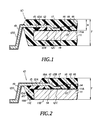
- the connector leads 12 is coupled to the contact pads 13 by the bonding wires 16 to electrically interconnect both of them.
- the bonding wires 16 have one end thereof bonded to the conductor leads 12 at the offset portion 12C thereof covered with the silver layer 17.
- the silver layer 17 advantageously serves as facilitating the thermo compression bonding of the one end of the bonding wires 16 to the offset portions 12C by means of ultrasonic waves, for example.
- the bonding wires 16 have the other end coupled to the contact pads 13.
Landscapes
- Engineering & Computer Science (AREA)
- Computer Hardware Design (AREA)
- Microelectronics & Electronic Packaging (AREA)
- Power Engineering (AREA)
- Physics & Mathematics (AREA)
- Condensed Matter Physics & Semiconductors (AREA)
- General Physics & Mathematics (AREA)
- Geometry (AREA)
- Wire Bonding (AREA)
- Structures Or Materials For Encapsulating Or Coating Semiconductor Devices Or Solid State Devices (AREA)
- Lead Frames For Integrated Circuits (AREA)
Priority Applications (1)
| Application Number | Priority Date | Filing Date | Title |
|---|---|---|---|
| EP03027952A EP1396886A3 (fr) | 1995-06-21 | 1996-06-18 | Dispositif semi-conducteur ayant l'extrémité interne de conducteurs disposée sur la surface d'une puce semi-conducteur |
Applications Claiming Priority (2)
| Application Number | Priority Date | Filing Date | Title |
|---|---|---|---|
| JP17829695 | 1995-06-21 | ||
| JP178296/95 | 1995-06-21 |
Related Child Applications (1)
| Application Number | Title | Priority Date | Filing Date |
|---|---|---|---|
| EP03027952A Division EP1396886A3 (fr) | 1995-06-21 | 1996-06-18 | Dispositif semi-conducteur ayant l'extrémité interne de conducteurs disposée sur la surface d'une puce semi-conducteur |
Publications (2)
| Publication Number | Publication Date |
|---|---|
| EP0750342A2 true EP0750342A2 (fr) | 1996-12-27 |
| EP0750342A3 EP0750342A3 (fr) | 1997-10-08 |
Family
ID=16045997
Family Applications (2)
| Application Number | Title | Priority Date | Filing Date |
|---|---|---|---|
| EP03027952A Withdrawn EP1396886A3 (fr) | 1995-06-21 | 1996-06-18 | Dispositif semi-conducteur ayant l'extrémité interne de conducteurs disposée sur la surface d'une puce semi-conducteur |
| EP96304531A Ceased EP0750342A3 (fr) | 1995-06-21 | 1996-06-18 | Dispositif semi-conducteur ayant l'extrémité interne de conducteurs disposée sur la surface d'une puce semi-conducteur |
Family Applications Before (1)
| Application Number | Title | Priority Date | Filing Date |
|---|---|---|---|
| EP03027952A Withdrawn EP1396886A3 (fr) | 1995-06-21 | 1996-06-18 | Dispositif semi-conducteur ayant l'extrémité interne de conducteurs disposée sur la surface d'une puce semi-conducteur |
Country Status (4)
| Country | Link |
|---|---|
| US (1) | US5874783A (fr) |
| EP (2) | EP1396886A3 (fr) |
| KR (1) | KR100473464B1 (fr) |
| TW (1) | TW314650B (fr) |
Cited By (3)
| Publication number | Priority date | Publication date | Assignee | Title |
|---|---|---|---|---|
| EP0801424A2 (fr) * | 1996-04-10 | 1997-10-15 | Oki Electric Industry Co., Ltd. | Dispositif semi-conducteur et procédé pour son assemblage |
| EP0807973A2 (fr) * | 1996-05-16 | 1997-11-19 | Oki Electric Industry Co., Ltd. | Dispositif semi-conducteur du type à incapsulation en plastique et procédé de fabrication |
| EP0884780A2 (fr) * | 1997-06-12 | 1998-12-16 | Nec Corporation | Dispositif semiconducteur à structure d'adhésion conducteur-puce amélioriée et cadre conducteur utilisé à cet effet |
Families Citing this family (9)
| Publication number | Priority date | Publication date | Assignee | Title |
|---|---|---|---|---|
| JPH10214933A (ja) * | 1997-01-29 | 1998-08-11 | Toshiba Corp | 半導体装置とその製造方法 |
| JP3638750B2 (ja) * | 1997-03-25 | 2005-04-13 | 株式会社ルネサステクノロジ | 半導体装置 |
| JP3085278B2 (ja) * | 1998-05-01 | 2000-09-04 | 日本電気株式会社 | 半導体装置の製造方法および半導体製造装置 |
| JP2001156237A (ja) * | 1999-11-25 | 2001-06-08 | Mitsubishi Electric Corp | リードフレーム及びそれを用いた樹脂封止型半導体装置 |
| US6664649B2 (en) * | 2001-02-28 | 2003-12-16 | Siliconware Precision Industries Co., Ltd. | Lead-on-chip type of semiconductor package with embedded heat sink |
| US7294533B2 (en) * | 2003-06-30 | 2007-11-13 | Intel Corporation | Mold compound cap in a flip chip multi-matrix array package and process of making same |
| US7495321B2 (en) * | 2006-07-24 | 2009-02-24 | Stats Chippac, Ltd. | Leaded stacked packages having elevated die paddle |
| TW200941669A (en) * | 2008-03-28 | 2009-10-01 | Powertech Technology Inc | Semiconductor packing structure |
| CN107954393B (zh) | 2011-08-24 | 2021-06-22 | 大陆-特韦斯贸易合伙股份公司及两合公司 | 具有唯一的电支承件的传感器 |
Citations (3)
| Publication number | Priority date | Publication date | Assignee | Title |
|---|---|---|---|---|
| US5221642A (en) * | 1991-08-15 | 1993-06-22 | Staktek Corporation | Lead-on-chip integrated circuit fabrication method |
| US5252853A (en) * | 1991-09-19 | 1993-10-12 | Mitsubishi Denki Kabushiki Kaisha | Packaged semiconductor device having tab tape and particular power distribution lead structure |
| US5406028A (en) * | 1991-03-20 | 1995-04-11 | Hitachi, Ltd. | Packaged semiconductor device having stress absorbing film |
Family Cites Families (16)
| Publication number | Priority date | Publication date | Assignee | Title |
|---|---|---|---|---|
| JPS5854644A (ja) * | 1981-09-28 | 1983-03-31 | Nec Corp | ボンデイング用樹脂基板 |
| JPS5966157A (ja) * | 1982-10-08 | 1984-04-14 | Fujitsu Ltd | 半導体装置及びその製造方法 |
| KR0158868B1 (ko) * | 1988-09-20 | 1998-12-01 | 미다 가쓰시게 | 반도체장치 |
| JP2895920B2 (ja) * | 1990-06-11 | 1999-05-31 | 株式会社日立製作所 | 半導体装置及びその製造方法 |
| JPH04320390A (ja) * | 1991-04-19 | 1992-11-11 | Hitachi Ltd | 表面実装型半導体部品の実装方法 |
| JP2509422B2 (ja) * | 1991-10-30 | 1996-06-19 | 三菱電機株式会社 | 半導体装置及びその製造方法 |
| US5229639A (en) * | 1991-10-31 | 1993-07-20 | International Business Machines Corporation | Low powder distribution inductance lead frame for semiconductor chips |
| KR940007757Y1 (ko) * | 1991-11-14 | 1994-10-24 | 금성일렉트론 주식회사 | 반도체 패키지 |
| JPH05152495A (ja) * | 1991-11-26 | 1993-06-18 | Hitachi Ltd | 半導体装置 |
| JP3410752B2 (ja) * | 1992-04-14 | 2003-05-26 | 富士通株式会社 | 半導体装置及びその製造方法 |
| JPH06132339A (ja) * | 1992-10-19 | 1994-05-13 | Mitsubishi Electric Corp | 半導体装置 |
| JP2934357B2 (ja) * | 1992-10-20 | 1999-08-16 | 富士通株式会社 | 半導体装置 |
| KR100269281B1 (ko) * | 1992-12-17 | 2000-10-16 | 윤종용 | 반도체장치 |
| JPH06216282A (ja) * | 1993-01-19 | 1994-08-05 | Hitachi Ltd | 樹脂封止型半導体装置 |
| JP2810626B2 (ja) * | 1994-06-07 | 1998-10-15 | 日鉄セミコンダクター株式会社 | 半導体装置 |
| US5545921A (en) * | 1994-11-04 | 1996-08-13 | International Business Machines, Corporation | Personalized area leadframe coining or half etching for reduced mechanical stress at device edge |
-
1996
- 1996-06-17 TW TW085107308A patent/TW314650B/zh not_active IP Right Cessation
- 1996-06-18 EP EP03027952A patent/EP1396886A3/fr not_active Withdrawn
- 1996-06-18 EP EP96304531A patent/EP0750342A3/fr not_active Ceased
- 1996-06-20 KR KR1019960022704A patent/KR100473464B1/ko not_active IP Right Cessation
-
1997
- 1997-07-25 US US08/900,469 patent/US5874783A/en not_active Expired - Lifetime
Patent Citations (3)
| Publication number | Priority date | Publication date | Assignee | Title |
|---|---|---|---|---|
| US5406028A (en) * | 1991-03-20 | 1995-04-11 | Hitachi, Ltd. | Packaged semiconductor device having stress absorbing film |
| US5221642A (en) * | 1991-08-15 | 1993-06-22 | Staktek Corporation | Lead-on-chip integrated circuit fabrication method |
| US5252853A (en) * | 1991-09-19 | 1993-10-12 | Mitsubishi Denki Kabushiki Kaisha | Packaged semiconductor device having tab tape and particular power distribution lead structure |
Non-Patent Citations (4)
| Title |
|---|
| PATENT ABSTRACTS OF JAPAN vol. 016, no. 230 (E-1208), 27 May 1992 & JP 04 044347 A (HITACHI LTD), 14 February 1992, * |
| PATENT ABSTRACTS OF JAPAN vol. 017, no. 156 (E-1341), 26 March 1993 & JP 04 320390 A (HITACHI LTD), 11 November 1992, * |
| PATENT ABSTRACTS OF JAPAN vol. 017, no. 538 (E-1440), 28 September 1993 & JP 05 152495 A (HITACHI LTD), 18 June 1993, * |
| PATENT ABSTRACTS OF JAPAN vol. 096, no. 004, 30 April 1996 & JP 07 335818 A (NITTETSU SEMICONDUCTOR KK), 22 December 1995, * |
Cited By (9)
| Publication number | Priority date | Publication date | Assignee | Title |
|---|---|---|---|---|
| EP0801424A2 (fr) * | 1996-04-10 | 1997-10-15 | Oki Electric Industry Co., Ltd. | Dispositif semi-conducteur et procédé pour son assemblage |
| EP0801424A3 (fr) * | 1996-04-10 | 1997-10-22 | Oki Electric Ind Co Ltd | |
| US6097083A (en) * | 1996-04-10 | 2000-08-01 | Oki Electric Industry Co., Ltd. | Semiconductor device which is crack resistant |
| EP0807973A2 (fr) * | 1996-05-16 | 1997-11-19 | Oki Electric Industry Co., Ltd. | Dispositif semi-conducteur du type à incapsulation en plastique et procédé de fabrication |
| EP0807973A3 (fr) * | 1996-05-16 | 1999-08-04 | Oki Electric Industry Co., Ltd. | Dispositif semi-conducteur du type à incapsulation en plastique et procédé de fabrication |
| EP1406299A1 (fr) * | 1996-05-16 | 2004-04-07 | Oki Electric Industry Company, Limited | Dispositif semi-conducteur moulé dans du plastique et son procédé de fabrication |
| EP0884780A2 (fr) * | 1997-06-12 | 1998-12-16 | Nec Corporation | Dispositif semiconducteur à structure d'adhésion conducteur-puce amélioriée et cadre conducteur utilisé à cet effet |
| EP0884780A3 (fr) * | 1997-06-12 | 2000-01-12 | Nec Corporation | Dispositif semiconducteur à structure d'adhésion conducteur-puce amélioriée et cadre conducteur utilisé à cet effet |
| US6211573B1 (en) | 1997-06-12 | 2001-04-03 | Nec Corporation | Semiconductor device with an improved lead-chip adhesion structure and lead frame to be used therefor |
Also Published As
| Publication number | Publication date |
|---|---|
| EP1396886A2 (fr) | 2004-03-10 |
| KR970003884A (ko) | 1997-01-29 |
| TW314650B (fr) | 1997-09-01 |
| EP0750342A3 (fr) | 1997-10-08 |
| US5874783A (en) | 1999-02-23 |
| EP1396886A3 (fr) | 2004-07-07 |
| KR100473464B1 (ko) | 2005-05-17 |
Similar Documents
| Publication | Publication Date | Title |
|---|---|---|
| US7145222B2 (en) | Leadless semiconductor package | |
| US6177718B1 (en) | Resin-sealed semiconductor device | |
| KR100386061B1 (ko) | 크랙을방지하기위한개량된구조를가지는반도체장치및리이드프레임 | |
| US6307257B1 (en) | Dual-chip integrated circuit package with a chip-die pad formed from leadframe leads | |
| US7514771B2 (en) | Leadless lead-frame | |
| KR100192028B1 (ko) | 플라스틱 밀봉형 반도체 장치 | |
| KR19980058198A (ko) | 버텀리드 반도체 패키지 | |
| EP0750342A2 (fr) | Dispositif semi-conducteur ayant l'extrémité interne de conducteurs disposée sur la surface d'une puce semi-conducteur | |
| KR19980032479A (ko) | 표면 설치 to-220 패키지 및 그의 제조 공정 | |
| US6495908B2 (en) | Multi-chip semiconductor package | |
| US5796160A (en) | Resin-sealed semiconductor device | |
| JP2857648B2 (ja) | 電子部品の製造方法 | |
| US6677662B1 (en) | Clamp and heat block assembly for wire bonding a semiconductor package assembly | |
| JPH05211262A (ja) | 樹脂封止型半導体装置 | |
| JP3427492B2 (ja) | 凸型ヒートシンク付き半導体装置及びその凸型ヒートシンクの製造方法 | |
| US6211563B1 (en) | Semiconductor package with an improved leadframe | |
| JP3454192B2 (ja) | リードフレームとそれを用いた樹脂封止型半導体装置およびその製造方法 | |
| KR100308899B1 (ko) | 반도체패키지및그제조방법 | |
| KR100304922B1 (ko) | 리드프레임및이를이용한반도체패키지 | |
| JPH0786335A (ja) | 半導体の実装構造とこれに用いる樹脂封止型半導体装置 | |
| KR19980037349A (ko) | 고 열방출용 리드 프레임 및 그를 이용한 반도체 칩 패키지 | |
| JP3406147B2 (ja) | 半導体装置 | |
| JP2577879B2 (ja) | 半導体装置 | |
| JPH11219969A (ja) | 半導体装置 | |
| KR200167587Y1 (ko) | 반도체 패캐이지 |
Legal Events
| Date | Code | Title | Description |
|---|---|---|---|
| PUAI | Public reference made under article 153(3) epc to a published international application that has entered the european phase |
Free format text: ORIGINAL CODE: 0009012 |
|
| AK | Designated contracting states |
Kind code of ref document: A2 Designated state(s): DE FR GB NL |
|
| PUAL | Search report despatched |
Free format text: ORIGINAL CODE: 0009013 |
|
| AK | Designated contracting states |
Kind code of ref document: A3 Designated state(s): DE FR GB NL |
|
| 17P | Request for examination filed |
Effective date: 19980312 |
|
| 17Q | First examination report despatched |
Effective date: 20000831 |
|
| STAA | Information on the status of an ep patent application or granted ep patent |
Free format text: STATUS: THE APPLICATION HAS BEEN REFUSED |
|
| 18R | Application refused |
Effective date: 20040612 |