EP0740340A2 - Struktur und Verfahren zur Montage eines Halbleiterchips - Google Patents
Struktur und Verfahren zur Montage eines Halbleiterchips Download PDFInfo
- Publication number
- EP0740340A2 EP0740340A2 EP96302414A EP96302414A EP0740340A2 EP 0740340 A2 EP0740340 A2 EP 0740340A2 EP 96302414 A EP96302414 A EP 96302414A EP 96302414 A EP96302414 A EP 96302414A EP 0740340 A2 EP0740340 A2 EP 0740340A2
- Authority
- EP
- European Patent Office
- Prior art keywords
- semiconductor chip
- layer
- metal
- side connectors
- powder
- Prior art date
- Legal status (The legal status is an assumption and is not a legal conclusion. Google has not performed a legal analysis and makes no representation as to the accuracy of the status listed.)
- Granted
Links
Images


Classifications
-
- H—ELECTRICITY
- H01—ELECTRIC ELEMENTS
- H01L—SEMICONDUCTOR DEVICES NOT COVERED BY CLASS H10
- H01L23/00—Details of semiconductor or other solid state devices
- H01L23/34—Arrangements for cooling, heating, ventilating or temperature compensation ; Temperature sensing arrangements
- H01L23/36—Selection of materials, or shaping, to facilitate cooling or heating, e.g. heatsinks
- H01L23/367—Cooling facilitated by shape of device
- H01L23/3675—Cooling facilitated by shape of device characterised by the shape of the housing
-
- H—ELECTRICITY
- H01—ELECTRIC ELEMENTS
- H01L—SEMICONDUCTOR DEVICES NOT COVERED BY CLASS H10
- H01L21/00—Processes or apparatus adapted for the manufacture or treatment of semiconductor or solid state devices or of parts thereof
- H01L21/02—Manufacture or treatment of semiconductor devices or of parts thereof
- H01L21/04—Manufacture or treatment of semiconductor devices or of parts thereof the devices having at least one potential-jump barrier or surface barrier, e.g. PN junction, depletion layer or carrier concentration layer
- H01L21/50—Assembly of semiconductor devices using processes or apparatus not provided for in a single one of the subgroups H01L21/06 - H01L21/326, e.g. sealing of a cap to a base of a container
- H01L21/56—Encapsulations, e.g. encapsulation layers, coatings
- H01L21/563—Encapsulation of active face of flip-chip device, e.g. underfilling or underencapsulation of flip-chip, encapsulation preform on chip or mounting substrate
-
- H—ELECTRICITY
- H01—ELECTRIC ELEMENTS
- H01L—SEMICONDUCTOR DEVICES NOT COVERED BY CLASS H10
- H01L23/00—Details of semiconductor or other solid state devices
- H01L23/28—Encapsulations, e.g. encapsulating layers, coatings, e.g. for protection
- H01L23/29—Encapsulations, e.g. encapsulating layers, coatings, e.g. for protection characterised by the material, e.g. carbon
-
- H—ELECTRICITY
- H01—ELECTRIC ELEMENTS
- H01L—SEMICONDUCTOR DEVICES NOT COVERED BY CLASS H10
- H01L23/00—Details of semiconductor or other solid state devices
- H01L23/28—Encapsulations, e.g. encapsulating layers, coatings, e.g. for protection
- H01L23/31—Encapsulations, e.g. encapsulating layers, coatings, e.g. for protection characterised by the arrangement or shape
- H01L23/3107—Encapsulations, e.g. encapsulating layers, coatings, e.g. for protection characterised by the arrangement or shape the device being completely enclosed
- H01L23/3135—Double encapsulation or coating and encapsulation
-
- H—ELECTRICITY
- H01—ELECTRIC ELEMENTS
- H01L—SEMICONDUCTOR DEVICES NOT COVERED BY CLASS H10
- H01L23/00—Details of semiconductor or other solid state devices
- H01L23/28—Encapsulations, e.g. encapsulating layers, coatings, e.g. for protection
- H01L23/31—Encapsulations, e.g. encapsulating layers, coatings, e.g. for protection characterised by the arrangement or shape
- H01L23/3157—Partial encapsulation or coating
- H01L23/3164—Partial encapsulation or coating the coating being a foil
-
- H—ELECTRICITY
- H01—ELECTRIC ELEMENTS
- H01L—SEMICONDUCTOR DEVICES NOT COVERED BY CLASS H10
- H01L23/00—Details of semiconductor or other solid state devices
- H01L23/48—Arrangements for conducting electric current to or from the solid state body in operation, e.g. leads, terminal arrangements ; Selection of materials therefor
- H01L23/488—Arrangements for conducting electric current to or from the solid state body in operation, e.g. leads, terminal arrangements ; Selection of materials therefor consisting of soldered or bonded constructions
- H01L23/498—Leads, i.e. metallisations or lead-frames on insulating substrates, e.g. chip carriers
- H01L23/49811—Additional leads joined to the metallisation on the insulating substrate, e.g. pins, bumps, wires, flat leads
- H01L23/49816—Spherical bumps on the substrate for external connection, e.g. ball grid arrays [BGA]
-
- H—ELECTRICITY
- H01—ELECTRIC ELEMENTS
- H01L—SEMICONDUCTOR DEVICES NOT COVERED BY CLASS H10
- H01L24/00—Arrangements for connecting or disconnecting semiconductor or solid-state bodies; Methods or apparatus related thereto
- H01L24/01—Means for bonding being attached to, or being formed on, the surface to be connected, e.g. chip-to-package, die-attach, "first-level" interconnects; Manufacturing methods related thereto
- H01L24/26—Layer connectors, e.g. plate connectors, solder or adhesive layers; Manufacturing methods related thereto
- H01L24/31—Structure, shape, material or disposition of the layer connectors after the connecting process
-
- H—ELECTRICITY
- H01—ELECTRIC ELEMENTS
- H01L—SEMICONDUCTOR DEVICES NOT COVERED BY CLASS H10
- H01L2224/00—Indexing scheme for arrangements for connecting or disconnecting semiconductor or solid-state bodies and methods related thereto as covered by H01L24/00
- H01L2224/01—Means for bonding being attached to, or being formed on, the surface to be connected, e.g. chip-to-package, die-attach, "first-level" interconnects; Manufacturing methods related thereto
- H01L2224/10—Bump connectors; Manufacturing methods related thereto
- H01L2224/15—Structure, shape, material or disposition of the bump connectors after the connecting process
- H01L2224/16—Structure, shape, material or disposition of the bump connectors after the connecting process of an individual bump connector
- H01L2224/161—Disposition
- H01L2224/16151—Disposition the bump connector connecting between a semiconductor or solid-state body and an item not being a semiconductor or solid-state body, e.g. chip-to-substrate, chip-to-passive
- H01L2224/16221—Disposition the bump connector connecting between a semiconductor or solid-state body and an item not being a semiconductor or solid-state body, e.g. chip-to-substrate, chip-to-passive the body and the item being stacked
- H01L2224/16225—Disposition the bump connector connecting between a semiconductor or solid-state body and an item not being a semiconductor or solid-state body, e.g. chip-to-substrate, chip-to-passive the body and the item being stacked the item being non-metallic, e.g. insulating substrate with or without metallisation
- H01L2224/16227—Disposition the bump connector connecting between a semiconductor or solid-state body and an item not being a semiconductor or solid-state body, e.g. chip-to-substrate, chip-to-passive the body and the item being stacked the item being non-metallic, e.g. insulating substrate with or without metallisation the bump connector connecting to a bond pad of the item
-
- H—ELECTRICITY
- H01—ELECTRIC ELEMENTS
- H01L—SEMICONDUCTOR DEVICES NOT COVERED BY CLASS H10
- H01L2224/00—Indexing scheme for arrangements for connecting or disconnecting semiconductor or solid-state bodies and methods related thereto as covered by H01L24/00
- H01L2224/01—Means for bonding being attached to, or being formed on, the surface to be connected, e.g. chip-to-package, die-attach, "first-level" interconnects; Manufacturing methods related thereto
- H01L2224/10—Bump connectors; Manufacturing methods related thereto
- H01L2224/15—Structure, shape, material or disposition of the bump connectors after the connecting process
- H01L2224/16—Structure, shape, material or disposition of the bump connectors after the connecting process of an individual bump connector
- H01L2224/161—Disposition
- H01L2224/16151—Disposition the bump connector connecting between a semiconductor or solid-state body and an item not being a semiconductor or solid-state body, e.g. chip-to-substrate, chip-to-passive
- H01L2224/16221—Disposition the bump connector connecting between a semiconductor or solid-state body and an item not being a semiconductor or solid-state body, e.g. chip-to-substrate, chip-to-passive the body and the item being stacked
- H01L2224/16245—Disposition the bump connector connecting between a semiconductor or solid-state body and an item not being a semiconductor or solid-state body, e.g. chip-to-substrate, chip-to-passive the body and the item being stacked the item being metallic
-
- H—ELECTRICITY
- H01—ELECTRIC ELEMENTS
- H01L—SEMICONDUCTOR DEVICES NOT COVERED BY CLASS H10
- H01L2224/00—Indexing scheme for arrangements for connecting or disconnecting semiconductor or solid-state bodies and methods related thereto as covered by H01L24/00
- H01L2224/01—Means for bonding being attached to, or being formed on, the surface to be connected, e.g. chip-to-package, die-attach, "first-level" interconnects; Manufacturing methods related thereto
- H01L2224/26—Layer connectors, e.g. plate connectors, solder or adhesive layers; Manufacturing methods related thereto
- H01L2224/28—Structure, shape, material or disposition of the layer connectors prior to the connecting process
- H01L2224/29—Structure, shape, material or disposition of the layer connectors prior to the connecting process of an individual layer connector
- H01L2224/29001—Core members of the layer connector
- H01L2224/29099—Material
- H01L2224/291—Material with a principal constituent of the material being a metal or a metalloid, e.g. boron [B], silicon [Si], germanium [Ge], arsenic [As], antimony [Sb], tellurium [Te] and polonium [Po], and alloys thereof
- H01L2224/29101—Material with a principal constituent of the material being a metal or a metalloid, e.g. boron [B], silicon [Si], germanium [Ge], arsenic [As], antimony [Sb], tellurium [Te] and polonium [Po], and alloys thereof the principal constituent melting at a temperature of less than 400°C
- H01L2224/29109—Indium [In] as principal constituent
-
- H—ELECTRICITY
- H01—ELECTRIC ELEMENTS
- H01L—SEMICONDUCTOR DEVICES NOT COVERED BY CLASS H10
- H01L2224/00—Indexing scheme for arrangements for connecting or disconnecting semiconductor or solid-state bodies and methods related thereto as covered by H01L24/00
- H01L2224/01—Means for bonding being attached to, or being formed on, the surface to be connected, e.g. chip-to-package, die-attach, "first-level" interconnects; Manufacturing methods related thereto
- H01L2224/26—Layer connectors, e.g. plate connectors, solder or adhesive layers; Manufacturing methods related thereto
- H01L2224/28—Structure, shape, material or disposition of the layer connectors prior to the connecting process
- H01L2224/29—Structure, shape, material or disposition of the layer connectors prior to the connecting process of an individual layer connector
- H01L2224/29001—Core members of the layer connector
- H01L2224/29099—Material
- H01L2224/291—Material with a principal constituent of the material being a metal or a metalloid, e.g. boron [B], silicon [Si], germanium [Ge], arsenic [As], antimony [Sb], tellurium [Te] and polonium [Po], and alloys thereof
- H01L2224/29101—Material with a principal constituent of the material being a metal or a metalloid, e.g. boron [B], silicon [Si], germanium [Ge], arsenic [As], antimony [Sb], tellurium [Te] and polonium [Po], and alloys thereof the principal constituent melting at a temperature of less than 400°C
- H01L2224/29111—Tin [Sn] as principal constituent
-
- H—ELECTRICITY
- H01—ELECTRIC ELEMENTS
- H01L—SEMICONDUCTOR DEVICES NOT COVERED BY CLASS H10
- H01L2224/00—Indexing scheme for arrangements for connecting or disconnecting semiconductor or solid-state bodies and methods related thereto as covered by H01L24/00
- H01L2224/01—Means for bonding being attached to, or being formed on, the surface to be connected, e.g. chip-to-package, die-attach, "first-level" interconnects; Manufacturing methods related thereto
- H01L2224/26—Layer connectors, e.g. plate connectors, solder or adhesive layers; Manufacturing methods related thereto
- H01L2224/28—Structure, shape, material or disposition of the layer connectors prior to the connecting process
- H01L2224/29—Structure, shape, material or disposition of the layer connectors prior to the connecting process of an individual layer connector
- H01L2224/29001—Core members of the layer connector
- H01L2224/29099—Material
- H01L2224/2919—Material with a principal constituent of the material being a polymer, e.g. polyester, phenolic based polymer, epoxy
-
- H—ELECTRICITY
- H01—ELECTRIC ELEMENTS
- H01L—SEMICONDUCTOR DEVICES NOT COVERED BY CLASS H10
- H01L2224/00—Indexing scheme for arrangements for connecting or disconnecting semiconductor or solid-state bodies and methods related thereto as covered by H01L24/00
- H01L2224/73—Means for bonding being of different types provided for in two or more of groups H01L2224/10, H01L2224/18, H01L2224/26, H01L2224/34, H01L2224/42, H01L2224/50, H01L2224/63, H01L2224/71
- H01L2224/732—Location after the connecting process
- H01L2224/73201—Location after the connecting process on the same surface
- H01L2224/73203—Bump and layer connectors
- H01L2224/73204—Bump and layer connectors the bump connector being embedded into the layer connector
-
- H—ELECTRICITY
- H01—ELECTRIC ELEMENTS
- H01L—SEMICONDUCTOR DEVICES NOT COVERED BY CLASS H10
- H01L2224/00—Indexing scheme for arrangements for connecting or disconnecting semiconductor or solid-state bodies and methods related thereto as covered by H01L24/00
- H01L2224/73—Means for bonding being of different types provided for in two or more of groups H01L2224/10, H01L2224/18, H01L2224/26, H01L2224/34, H01L2224/42, H01L2224/50, H01L2224/63, H01L2224/71
- H01L2224/732—Location after the connecting process
- H01L2224/73251—Location after the connecting process on different surfaces
- H01L2224/73257—Bump and wire connectors
-
- H—ELECTRICITY
- H01—ELECTRIC ELEMENTS
- H01L—SEMICONDUCTOR DEVICES NOT COVERED BY CLASS H10
- H01L2224/00—Indexing scheme for arrangements for connecting or disconnecting semiconductor or solid-state bodies and methods related thereto as covered by H01L24/00
- H01L2224/80—Methods for connecting semiconductor or other solid state bodies using means for bonding being attached to, or being formed on, the surface to be connected
- H01L2224/83—Methods for connecting semiconductor or other solid state bodies using means for bonding being attached to, or being formed on, the surface to be connected using a layer connector
- H01L2224/83909—Post-treatment of the layer connector or bonding area
- H01L2224/83951—Forming additional members, e.g. for reinforcing, fillet sealant
-
- H—ELECTRICITY
- H01—ELECTRIC ELEMENTS
- H01L—SEMICONDUCTOR DEVICES NOT COVERED BY CLASS H10
- H01L2924/00—Indexing scheme for arrangements or methods for connecting or disconnecting semiconductor or solid-state bodies as covered by H01L24/00
- H01L2924/01—Chemical elements
- H01L2924/01005—Boron [B]
-
- H—ELECTRICITY
- H01—ELECTRIC ELEMENTS
- H01L—SEMICONDUCTOR DEVICES NOT COVERED BY CLASS H10
- H01L2924/00—Indexing scheme for arrangements or methods for connecting or disconnecting semiconductor or solid-state bodies as covered by H01L24/00
- H01L2924/01—Chemical elements
- H01L2924/01006—Carbon [C]
-
- H—ELECTRICITY
- H01—ELECTRIC ELEMENTS
- H01L—SEMICONDUCTOR DEVICES NOT COVERED BY CLASS H10
- H01L2924/00—Indexing scheme for arrangements or methods for connecting or disconnecting semiconductor or solid-state bodies as covered by H01L24/00
- H01L2924/01—Chemical elements
- H01L2924/01013—Aluminum [Al]
-
- H—ELECTRICITY
- H01—ELECTRIC ELEMENTS
- H01L—SEMICONDUCTOR DEVICES NOT COVERED BY CLASS H10
- H01L2924/00—Indexing scheme for arrangements or methods for connecting or disconnecting semiconductor or solid-state bodies as covered by H01L24/00
- H01L2924/01—Chemical elements
- H01L2924/01019—Potassium [K]
-
- H—ELECTRICITY
- H01—ELECTRIC ELEMENTS
- H01L—SEMICONDUCTOR DEVICES NOT COVERED BY CLASS H10
- H01L2924/00—Indexing scheme for arrangements or methods for connecting or disconnecting semiconductor or solid-state bodies as covered by H01L24/00
- H01L2924/01—Chemical elements
- H01L2924/01024—Chromium [Cr]
-
- H—ELECTRICITY
- H01—ELECTRIC ELEMENTS
- H01L—SEMICONDUCTOR DEVICES NOT COVERED BY CLASS H10
- H01L2924/00—Indexing scheme for arrangements or methods for connecting or disconnecting semiconductor or solid-state bodies as covered by H01L24/00
- H01L2924/01—Chemical elements
- H01L2924/01029—Copper [Cu]
-
- H—ELECTRICITY
- H01—ELECTRIC ELEMENTS
- H01L—SEMICONDUCTOR DEVICES NOT COVERED BY CLASS H10
- H01L2924/00—Indexing scheme for arrangements or methods for connecting or disconnecting semiconductor or solid-state bodies as covered by H01L24/00
- H01L2924/01—Chemical elements
- H01L2924/0103—Zinc [Zn]
-
- H—ELECTRICITY
- H01—ELECTRIC ELEMENTS
- H01L—SEMICONDUCTOR DEVICES NOT COVERED BY CLASS H10
- H01L2924/00—Indexing scheme for arrangements or methods for connecting or disconnecting semiconductor or solid-state bodies as covered by H01L24/00
- H01L2924/01—Chemical elements
- H01L2924/01033—Arsenic [As]
-
- H—ELECTRICITY
- H01—ELECTRIC ELEMENTS
- H01L—SEMICONDUCTOR DEVICES NOT COVERED BY CLASS H10
- H01L2924/00—Indexing scheme for arrangements or methods for connecting or disconnecting semiconductor or solid-state bodies as covered by H01L24/00
- H01L2924/01—Chemical elements
- H01L2924/01042—Molybdenum [Mo]
-
- H—ELECTRICITY
- H01—ELECTRIC ELEMENTS
- H01L—SEMICONDUCTOR DEVICES NOT COVERED BY CLASS H10
- H01L2924/00—Indexing scheme for arrangements or methods for connecting or disconnecting semiconductor or solid-state bodies as covered by H01L24/00
- H01L2924/01—Chemical elements
- H01L2924/01047—Silver [Ag]
-
- H—ELECTRICITY
- H01—ELECTRIC ELEMENTS
- H01L—SEMICONDUCTOR DEVICES NOT COVERED BY CLASS H10
- H01L2924/00—Indexing scheme for arrangements or methods for connecting or disconnecting semiconductor or solid-state bodies as covered by H01L24/00
- H01L2924/01—Chemical elements
- H01L2924/0105—Tin [Sn]
-
- H—ELECTRICITY
- H01—ELECTRIC ELEMENTS
- H01L—SEMICONDUCTOR DEVICES NOT COVERED BY CLASS H10
- H01L2924/00—Indexing scheme for arrangements or methods for connecting or disconnecting semiconductor or solid-state bodies as covered by H01L24/00
- H01L2924/01—Chemical elements
- H01L2924/01051—Antimony [Sb]
-
- H—ELECTRICITY
- H01—ELECTRIC ELEMENTS
- H01L—SEMICONDUCTOR DEVICES NOT COVERED BY CLASS H10
- H01L2924/00—Indexing scheme for arrangements or methods for connecting or disconnecting semiconductor or solid-state bodies as covered by H01L24/00
- H01L2924/01—Chemical elements
- H01L2924/01074—Tungsten [W]
-
- H—ELECTRICITY
- H01—ELECTRIC ELEMENTS
- H01L—SEMICONDUCTOR DEVICES NOT COVERED BY CLASS H10
- H01L2924/00—Indexing scheme for arrangements or methods for connecting or disconnecting semiconductor or solid-state bodies as covered by H01L24/00
- H01L2924/01—Chemical elements
- H01L2924/01078—Platinum [Pt]
-
- H—ELECTRICITY
- H01—ELECTRIC ELEMENTS
- H01L—SEMICONDUCTOR DEVICES NOT COVERED BY CLASS H10
- H01L2924/00—Indexing scheme for arrangements or methods for connecting or disconnecting semiconductor or solid-state bodies as covered by H01L24/00
- H01L2924/01—Chemical elements
- H01L2924/01079—Gold [Au]
-
- H—ELECTRICITY
- H01—ELECTRIC ELEMENTS
- H01L—SEMICONDUCTOR DEVICES NOT COVERED BY CLASS H10
- H01L2924/00—Indexing scheme for arrangements or methods for connecting or disconnecting semiconductor or solid-state bodies as covered by H01L24/00
- H01L2924/01—Chemical elements
- H01L2924/01082—Lead [Pb]
-
- H—ELECTRICITY
- H01—ELECTRIC ELEMENTS
- H01L—SEMICONDUCTOR DEVICES NOT COVERED BY CLASS H10
- H01L2924/00—Indexing scheme for arrangements or methods for connecting or disconnecting semiconductor or solid-state bodies as covered by H01L24/00
- H01L2924/013—Alloys
- H01L2924/0132—Binary Alloys
-
- H—ELECTRICITY
- H01—ELECTRIC ELEMENTS
- H01L—SEMICONDUCTOR DEVICES NOT COVERED BY CLASS H10
- H01L2924/00—Indexing scheme for arrangements or methods for connecting or disconnecting semiconductor or solid-state bodies as covered by H01L24/00
- H01L2924/013—Alloys
- H01L2924/0132—Binary Alloys
- H01L2924/01322—Eutectic Alloys, i.e. obtained by a liquid transforming into two solid phases
-
- H—ELECTRICITY
- H01—ELECTRIC ELEMENTS
- H01L—SEMICONDUCTOR DEVICES NOT COVERED BY CLASS H10
- H01L2924/00—Indexing scheme for arrangements or methods for connecting or disconnecting semiconductor or solid-state bodies as covered by H01L24/00
- H01L2924/013—Alloys
- H01L2924/0133—Ternary Alloys
-
- H—ELECTRICITY
- H01—ELECTRIC ELEMENTS
- H01L—SEMICONDUCTOR DEVICES NOT COVERED BY CLASS H10
- H01L2924/00—Indexing scheme for arrangements or methods for connecting or disconnecting semiconductor or solid-state bodies as covered by H01L24/00
- H01L2924/15—Details of package parts other than the semiconductor or other solid state devices to be connected
- H01L2924/151—Die mounting substrate
- H01L2924/156—Material
- H01L2924/15786—Material with a principal constituent of the material being a non metallic, non metalloid inorganic material
- H01L2924/15787—Ceramics, e.g. crystalline carbides, nitrides or oxides
Definitions
- the present invention relates to a mounting structure for a semiconductor element and, specifically, to that for a face-down type wherein connecting sections formed on a mounting surface of a circuit board on which a semiconductor element is to be mounted are electrically connected to those formed on one surface of the semiconductor element opposite to the mounting surface, and to a method for mounting the semiconductor element.
- a face-down type mounting structure as shown in Fig. 18 and hereinafter referred merely to a mounting structure, has been used as a mounting structure for a semiconductor element enabling very dense connections.
- connection terminals 204 such as solder bumps are provided, as circuit board side connecting sections, on one surface of a semiconductor element 202 opposite to a mounting surface of a circuit board 200 on which the semiconductor element is mounted.
- connection terminals 204 is connected to each of connection pads 208 provided, as element side connecting sections, at an end or midway of each of circuit patterns 206 formed on the mounting surface of the circuit board 200, so that the electric connection is obtained between the semiconductor element and the circuit board.
- an insulating resin layer 210 is sometimes provided while exposing another surface of the semiconductor element 202 as shown in Fig. 19 for the purpose of sealing the element side connecting sections and the circuit board side connecting sections electrically connected to each other.
- a cap or the like is usually mounted to the semiconductor element 202 to seal the same.
- the resultant mounting structure is extremely complicated in structure, which requires a longer mounting process and a higher production cost and is accompanied by a lower yield.
- heat generated in the semiconductor element 202 must flow via a cap or the like for sealing the semiconductor element 202, which deteriorates the heat dissipation ability of the mounting structure whereby the heat tends to be stored in the mounting structure.
- the cap or the like for sealing the semiconductor element 202 is unnecessary and the other surface (back surface) of the semiconductor element can be brought into direct contact with the low melting point metal layer, the heat generated in the semiconductor element 202 can be easily dissipated from the mounting structure.
- the low melting point metal layer is usually brought into contact with the other surface of the semiconductor element 202 via a metalized layer of gold or the like coated on the semiconductor element 202 and also directly with the insulating resin layer 210.
- a molten metal having a low melting point has a good wettability to the metallic layer, but has an inferior wettability to the surface of the insulating resin layer 210.
- the low melting point metal layer is closely adhered to the other surface of the semiconductor element 202 via the metalized layer of gold or the like, it may separate from the insulating resin layer 210 on the boundary surface therebetween.
- the mounting structure of the semiconductor element proposed in the above Patent Publication has a poor durability and cannot to be put into practice.
- the mounting structure of the semiconductor element proposed in the above Patent Publication has a favorable property for dissipating the heat generated in the semiconductor element, it is suitable as a mounting structure for a semiconductor element generating a large amount of heat.
- an object of the present invention is to provide a mounting structure of a semiconductor element, and a method for mounting a semiconductor element, capable of preventing separation between an insulating resin layer and a layer of a metal having a low melting point covering the semiconductor element or others, which resin layer is formed by filling an insulating resin in a gap between one surface of a semiconductor element mounted onto a circuit board and a mounting surface of the circuit board, so that the durability and the heat dissipation ability are improved.
- the present inventors have studied to achieve the above object and have found that the wettability of the insulating resin layer to the molten metal having a low melting point is enhanced by bonding metallic powder on the surface of the resin layer, and have thus completed the present invention.
- an semiconductor chip mount structure comprising: a substrate having a base surface on which base side connectors are formed; a semiconductor chip mounted on the base surface of the substrate, the semiconductor chip having chip side connectors on a first surface thereof facing the base surface of the substrate, the chip side connectors being electrically connected to the base side connectors; an insulation resin layer arranged so as to cover connecting portions including the chip side connectors and the base side connectors; a metal layer, consisting of a metal having a melting point lower than an endurance temperature of the semiconductor chip, for covering the semiconductor chip and the insulation resin layer; and a wetting characteristic improved layer formed along at least a part of a contact surface between the metal layer and the insulation resin layer.
- the metal layer also covers at least a part of the base surface of the substrate and a second wetting characteristic improved layer is formed along at least a part of a second contact surface between the metal layer and the base surface of the substrate.
- the semiconductor chip has a second surface, which is exposed from the insulation resin layer but is covered by the metal layer.
- a heat radiation member such as a heat spreader or fin member, is provided on the metal layer adjacent to the second surface of the semiconductor chip.
- the metal layer essentially consists of a low melting point metal, such as solder, which melts at a temperature lower than 450°.
- the low melting point metal layer consists of a low melting point base metal and a metal powder mixed in the base metal and having a melting point higher than that of the base metal.
- the metal powder is one or a mixture of two or more selected from a group consisting of tungsten (W) powder, molybdenum (Mo) powder, silver (Ag) powder and copper (Cu) powder.
- the low melting point metal layer consists of a base metal and an inorganic powder mixed in the base metal and having a melting point higher than that of the base metal.
- the inorganic powder is one or a mixture of two or more selected form a group consisting of silicon dioxide (SiO 2 ) powder, silicon carbide (SiC) powder, aluminum nitride (AlN) powder, boron nitride (BN) powder and carbon (C) powder.
- the insulation resin layer comprises an insulation inorganic powder, such as silicon dioxide (SiO 2 ) powder.
- the wetting characteristic improved layer is a metal powder or metal foil layer attached onto the insulation resin layer which is in contact with the metal layer.
- the metal powder or metal foil layer may consist of a metal having a melting point higher than that of the melting point of the metal layer.
- the second wetting characteristic improved layer is a metal powder or metal foil layer attached onto the base surface of the substrate which is in contact with the metal layer.
- the metal powder or metal foil layer consists of a metal having a melting point higher than that of the melting point of the metal layer.
- the base side connectors formed on the base surface of the substrate comprises at least one ground pattern and the metal layer electrically connected to the ground pattern.
- the chip side connectors are electrically connected to the base side connectors by means of connecting terminals, such as solder bumps, mounted on the semiconductor chip.
- the chip side connectors are electrically connected to the base side connectors by means of a tape automated bonding tape having a conductive pattern.
- a plurality of semiconductor chips are mounted on the base surface of the substrate, the semiconductor chips having respective chip side connectors which are electrically connected to the base side connectors, the insulation resin layer being arranged so as to cover connecting portions including the chip side connectors and the base side connectors, and the metal layer covering the insulation resin layer and the plurality of semiconductor chips.
- the substrate having the base surface on which the base side connectors are formed comprises a flexible film.
- a process for mounting a semiconductor chip, having chip side connectors on a first surface thereof, on a substrate having a base surface on which base side connectors are formed comprising the steps of; mounting a semiconductor chip, on the base surface of the substrate, so that chip side connectors of the semiconductor chip are electrically connected to the base side connectors; filling an insulation resin into a gap between the base surface of the substrate and the first surface of the semiconductor chip to cover connecting portions including the chip side connectors and the base side connectors; forming a wetting characteristic improved layer on at least a part of an exposed surface of the insulation resin layer, the wetting characteristic of the wetting characteristic improved layer with respect to a low melting point metal layer is at least better than that of the insulation resin, and forming the metal layer, consisting of a metal having a melting point lower than an endurance temperature of the semiconductor chip, for covering the semiconductor chip and the insulation resin layer.
- a process for mounting a semiconductor chip, having chip side connectors on a first surface thereof, on a substrate having a base surface on which base side connectors are formed comprising the following steps of: mounting a semiconductor chip on the base surface of the substrate, so that chip side connectors of the semiconductor chip are electrically connected to the base side connectors; filling an insulation resin into a gap between the base surface of the substrate and the first surface of the semiconductor chip to cover connecting portions including the chip side connectors and the base side connectors; forming first and second wetting characteristic improved layers on at least a part of an exposed surface of the insulation resin layer and at least a part of the base surface of the substrate, respectively, the wetting characteristic of the first and second wetting characteristic improved layers with respect to a low melting point metal layer is at least better than that of the insulation resin and the base surface of the substrate, respectively; forming the first and second metal layers, consisting of a metal having a melting point lower than an endurance temperature of the semiconductor chip, for covering the
- the present invention since the other surface of the semiconductor element is exposed from the insulating resin layer and coated with the low melting point metal layer, it is possible to bring the low melting point metal layer into direct contact with the other surface of the semiconductor element to further improve the ability for dissipating the heat generated in the semiconductor element.
- the surface of an insulating resin layer formed of an insulating resin filled in a gap between one surface of a semiconductor element and a mounting surface of a circuit board has a poor wettability to a molten metal having a low melting point, and thus repels the latter. Accordingly, the insulating resin layer is easily separated from the low melting point metal layer.
- a wettability improvement layer consisting of metallic powder is formed on at least part of the insulating resin layer and has an improved wettability to the molten metal having a lower melting point.
- the heat conductivity of the low melting point metal layer is enhanced to further improve the heat dissipation ability of the mounting structure.
- an inorganic substance powder having a melting point higher than that of the low melting point metal is contained, the difference in the thermal expansion coefficient between the semiconductor element and the low melting point metal layer can be as small as possible to further enhance the durability of the mounting structure of the semiconductor element.
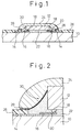
- the mounting structure of the semiconductor element according to the present invention is a face-down type wherein connecting sections provided on a mounting surface of a circuit board on which a semiconductor element is mounted are electrically connected to those provided on one surface of the semiconductor element opposite to the mounting surface.
- Fig. 1 shows such a face-down type mounting structure, wherein a plurality of connection pads 16 are formed at the extremities of, or at the midway of, circuit patterns 14 provided, as circuit board side connecting sections, on a mounting surface of a circuit board 10 made of ceramic or plastic carrying a semiconductor element 12.
- the circuit board 10 may have internal circuit patterns. Also, such a circuit board 10 may either be a ball-grid-array (BGA) type having solder bumps as external terminals or a pin-grid-array (PGA) type having lead pins as external terminals.
- BGA ball-grid-array
- PGA pin-grid-array
- connection terminals (bumps) 18 are provided, as element side connecting sections, on one surface of the semiconductor element 10 opposite to the mounting surface of the circuit board 10.
- Each of the terminals (bumps) 18 of the semiconductor element 10 is connected to each of the connection pads 16 via a conductor pattern 20 of a TAB (tap automated bonding) tape to achieve the electric connection between the semiconductor element 12 and the circuit board 10.
- TAB tape automated bonding
- the joint portion between the semiconductor element 12 and the circuit board 10 is sealed by an insulating resin layer 22 while exposing the other surface of the semiconductor element 12.
- Insulating resins used for forming such an insulating resin layer 22 may be known ones conventionally used for sealing a semiconductor element, in which an epoxy type resin is suitable.
- An organic insulating component is preferably contained therein as a filler, such as silicon dioxide (SiO 2 ), for improving the heat conductivity of the insulating resin layer 22.
- the circuit patterns 14 formed on the mounting surface of the circuit board 10 are insulated by a resin film 26 formed of an insulating resin such as polyimide resin, except for the connection pads 16 used as circuit board side connecting sections.
- the insulating resin layer 22 and the other surface of the semiconductor element 12 are coated by a low melting point metal layer 24.
- a metal used for forming the low melting point metal layer 24 has a melting point lower than a heat durable temperature of the semiconductor element 12.
- the melting point of the low melting point metal is 450°C or lower.
- the melting point exceeds 450°C , problems on thermal durability of the semiconductor element 12 are liable to occur. On such a view point, it is preferable to use low melting point metals which melt at 250°C or lower.
- the low melting point metal may be an alloy used for brazing and preferably solder an alloy.
- solder alloys are Sn-Pb type, Sn-Pb-Sb type, Sn-Pb-Ag type, Pb-In type, Pb-Ag type, Sn-Zn type, Sn-Sb type, Sn-Ag type, and Bi-Sn-In type.
- the "heat durable temperature" of the semiconductor element 12 referred to in the present invention is such a temperature that, if exceeding this temperature, the circuits or other components on the semiconductor element 12 may be thermally destroyed.
- the low melting point metal layer 24 formed of such a low melting point metal and the other surface of the semiconductor element 12 are closely bonded with each other usually via a metalized layer of gold or others on the semiconductor element 12, while the resin layer 26 and the low melting point metal layer 24 are closely bonded with each other via metal layers 28 formed as wettability improvement layers on the surface of the resin layer 26 with a foil of copper or other metal or by electroless plating or by sputtering.
- the low melting metal layer 24 and the insulating resin layer 22 are closely bonded to each other via a wettability improvement layer formed on the surface of the insulating resin layer 22, having the improved wettability to the molten metal having a low melting point.
- the wettability improvement layer is preferably a metallic powder layer 30 consisting of a metallic powder bonded to the surface of the insulating resin layer 22, as shown in Fig. 2.
- This metallic powder layer 30 can be formed by spreading the metallic powder on the surface of the insulating resin layer 22, and thereafter curing the insulating resin layer 22 in a heated atmosphere. Particularly, if the metallic powder is spread on the surface of the insulating resin layer during the latter has not been fully hardened, the metallic powder is more preferably attached thereon.
- Metallic powder used for this purpose has a melting point higher than that of the low melting point metal forming the lower melting point metal layer, wherein one or a mixture of two or more kinds of powders, selected from the group consisting of tungsten (W) powder, molybdenum (Mo) powder, silver (Ag) powder and copper (Cu) powder may be suitably used.
- W tungsten
- Mo molybdenum
- Cu copper
- a metal layer 32 formed on part of the surface of the insulating resin layer 22 may be used as the wettability improvement layer as shown in Fig. 3.
- the metal layer 32 is formed on a flattened portion of the surface of the insulating resin layer 22 by a foil of copper or other metal having a melting point higher than that of the low melting point metal, or by plating such a metal.
- the metallic layer 32 is formed by a plating, part of the surface of the insulating resin layer 22 need not be flattened.
- the adhesion between the insulating resin layer 22 and the low melting point metal layer 24 can also be enhanced by the formation of the wettability improvement layer on part of the surface of the insulating resin layer 22, having an improved wettability compared with the other surface of the insulating resin layer 22.
- the heat conductivity of the low melting point metal forming the low melting point metal layer 24 according to the present invention is at most 80 W/m° K, which can be further enhanced by mixing a metallic powder having a melting point higher than that of the low melting point metal in the low melting point metal layer 24.
- the metallic powder used for this purpose is one or a mixture of two or more kinds selected from a group consisting of tungsten (W) powder, molybdenum (Mo) powder, silver (Ag) powder and copper (Cu) powder.
- the low melting point metal layer 24 containing a powder of tungsten (W) or molybdenum (Mo) has a lower thermal expansion coefficient compared with that formed solely of the low melting point metal.
- W tungsten
- Mo molybdenum
- the low melting point metal layer 24 containing a powder of tungsten (W) or molybdenum (Mo) has a lower thermal expansion coefficient compared with that formed solely of the low melting point metal.
- the thermal expansion coefficient of the resultant low melting point metal layer 24 is improved to about 6 ⁇ 10 -6 through 8 ⁇ 10 -6 /°C.
- thermal and mechanical stress which may occur due to the difference in the thermal expansion between the semiconductor element 12 and the low melting point metal layer 24, can be reduced to a great extent.
- a powder of an inorganic substance having a melting point higher than that of the low melting point metal layer 24 may be added.
- the inorganic substance powder used therefor is one or more kinds of powders selected from a group of silicon dioxide (SiO 2 ) powder, silicon carbide (SiC) powder, aluminum nitride (AlN) powder, boron nitride (BN) powder and carbon (C) powder.
- silicon carbide (SiC) powder, aluminum nitride (AlN) powder, boron nitride (BN) powder and carbon (C) powder are used as the inorganic substance powder, it is possible to maintain or improve the thermal conductivity of the resultant low melting point metal layer 24.
- a flux is preferably added thereto for the purpose of improving the wettability of the metallic powder to the low melting point metal.
- the favorable flux used for a copper powder is of an organic type such as rosin type flux, while that used for a tungsten or molybdenum powder is of an inorganic type such as hydrochloric acid.
- the inorganic type flux such as hydrochloric acid
- the wettability to the low melting point metal is lower than that obtained when the metallic powder such as silver (Ag) powder or copper (Cu) powder is mixed.
- the inorganic substance powder such as silicon dioxide (SiO 2 ) powder, silicon carbide (SiC) powder, aluminum nitride (AlN) powder, boron nitride (BN) powder or carbon (C) powder is mixed with the low melting point metal, it is difficult to improve the wettability of the metallic powder to the low melting point metal solely by the addition of the flux.
- the metallic powder such as tungsten or molybdenum or the inorganic substance powder
- a metallic layer can be formed through electroless plating, ion plating or flame spraying, or by the use of a coupling agent, or via a mixing dry mill.
- boron nitride (BN) or carbon (C) powder it is difficult to provide a metal layer having a sufficient strength for forming a compact layer 24 of the low melting point metal, whereby such a powder is unsuitable for the purpose of maintaining the air-tight state by coating the semiconductor element 12 with the low melting point metal layer 24.
- both the layers 22, 24 are closely adhered to each other to improve the durability of the mounting structure.
- the low melting point metal layer 24 is brought into direct contact with the other surface of the semiconductor element 12, it is possible to promptly dissipate heat generated in the semiconductor element 12 to stop the heat being stored in the mounting structure.
- each of the connection pads 16 provided, as circuit board side connecting sections, on the mounting surface of the circuit board 10 carrying the semiconductor element 12 is connected to each of the connection terminals 18 provided, as element side connecting sections, on one surface of the semiconductor element 12 opposite to the mounting surface of the circuit board 10, via the conductor patterns 20 of TAB tape formed on the mounting surface of the circuit board 10.
- the resin film 26 consisting of an insulating resin such as polyimide is provided on the mounting surface of the circuit board 10, except for the connection pads 16.
- an insulating resin such as epoxy type resin is filled in a gap between the mounting surface of the circuit board 10 and one surface of the semiconductor element 12 to form the insulating resin layer 22 while exposing the other surface of the semiconductor element 12 therefrom. If an insulating inorganic component such as a filler of silicon dioxide (SiO 2 ,) is mixed into the insulating resin, the heat conductivity of the insulating resin layer 22 can be improved.
- the resin film 26 may be formed prior to mounting the semiconductor element 12.
- the metallic powder layer 30 or the metal layer 32 is formed, as a layer having the improved wettability to a molten low melting point metal such as a solder alloy, on at least part of the exposed surface of the insulating resin layer 22.
- the metallic powder layer 30 can be formed by spreading one or more kinds of metallic powders having a melting point higher than that of a metal forming the low melting point metal layer 24, selected from a group consisting of tungsten (W) powder, molybdenum (Mo) powder, silver (Ag) powder and copper (Cu) powder, on the insulating resin layer 22, and curing a insulating resin layer 22 in a heated atmosphere.
- the metallic layer 32 can also be formed by adhering a foil of metal having a melting point higher than that of the low melting point metal, such as copper, or by plating the same.
- the low melting point metal layer 24 is formed by melting a low melting point metal such as a solder alloy to cover the insulating resin layer 22 and the other surface of the semiconductor element 12.
- a low melting point metal such as a solder alloy
- metallic powders having the melting point higher than that of the low melting point metal selected from a group of tungsten (W) powder, molybdenum (Mo) powder, silver (Ag) powder and copper (Cu) powder are mixed in this low melting point metal to improve the heat conductivity of the bow melting point metal layer 24.
- the low melting point metal layer 24 if one or more kinds of inorganic substance powders are mixed, having the melting point higher than that of the low melting point metal, selected from a group consisting of silicon dioxide (SiO 2 ) powder, silicon carbide (SiC) powder, aluminum nitride (AlN) powder, boron nitride (BN) powder and C (carbon) powder, it is possible to minimize the difference in the thermal expansion coefficient between the low melting point metal layer 24 and the semiconductor element 12.
- silicon dioxide (SiO 2 ) powder silicon dioxide (SiO 2 ) powder, silicon carbide (SiC) powder, aluminum nitride (AlN) powder, boron nitride (BN) powder and C (carbon) powder
- These metallic powders and the inorganic substance powders may be used together.
- the electric connection between the semiconductor element 12 and the circuit patterns 14 is made, in the mounting structure stated above, by connecting each of the connection terminals 18 on the semiconductor element 12 to each of the connection pads 16 on the circuit board 10 via the conductor pattern 20 of TAB tape.
- This connection also may be done by connecting each of connection pads (electrodes of the semiconductor element) on the semiconductor element 12 to each of the connection pads 16 on the circuit board 10 via the conductor pattern 20 of TAB tape, as shown in Fig. 4.
- the heat dissipation ability of the mounting structure can be more enhanced by providing a heat radiation fin 34 for accelerating the heat dissipation on the outer surface of the low melting point metal layer 24.
- the heat radiation fin 34 may be replaced by a heat spreader or a water-cooled channel.
- connection between the semiconductor element 12 and the connection pads 16 of the circuit patterns 14 formed on the mounting surface of the circuit board 10 may be made via bumps 36 provided on the one surface of the semiconductor element 12 opposite to the mounting surface of the circuit board 10.
- a plurality of semiconductor elements 12a, 12b on a common circuit board and, after an insulating resin has been filled in a gap between one surface of the respective semiconductor element 12a, 12b and the mounting surface of the circuit board 10 so that insulating resin layers 22 are provided, form a low melting point metal layer 24 using a metal having a low melting point such as a solder alloy while covering the insulating resin layers 22 and the semiconductor elements 12a, 12b.
- the heat dissipation ability of the mounting structure can be further enhanced if a heat dissipation member such a heat radiation fin 34 or other is mounted onto the outer surface of the low melting point metal layer 24.
- the present invention includes a mounting structure wherein a semiconductor element 12 is mounted on a film type circuit board formed of a TAB tape 38 as shown in Fig. 7.
- the TAB tape 38 forming the mounting structure shown in Fig. 7 consists of a flexible base film 40 such as polyimide or epoxy film, on one surface of which are formed conductor patterns 42, wherein an inner leads 43 of the conductor patterns 42 project into a device hole from the periphery thereof, which is formed in the base film in an area corresponding to the semiconductor element 12.
- a silicon type insulating resin is coated on the mounting surface of the TAB tape 38, on which the semiconductor element 12 is to be mounted, to form a resin film 50, on the upper surface of which a metallic layer 28 is formed.
- solder bumps 44 are provided, as connection terminals for external circuits, on the respective connection pads formed in the conductor patterns 42.
- the end surfaces of the film circuit board are coated with an insulating resin to form resin layers 48 for the purpose of insulating between the conductor patterns 42.
- the joint portion between the semiconductor element 12 mounted onto the TAB tape 38 and the inner leads 43 thereof is sealed with an insulating resin layer 22 formed of an insulating resin such as epoxy type resin, but the other surface of the semiconductor element 12 is exposed outside the insulating resin layer 22.
- the other surface of the semiconductor element 12 and the insulating resin layer 22 is coated with a low melting point metal layer 24 formed of a metal having a low melting point such as a solder alloy. Both the layers are closely bonded with each other via a metallic powder layer 30 (Fig. 2) or a metal layer (Fig. 3) formed on at least part of the exposed surface of the insulating resin layer 22. Also, the resin film 50 and the low melting point metal layer 24 are closely bonded together via the metal layer 28 formed on the outer surface of the resin film 50 as a wettability improvement layer.
- a heat dissipating member such as a heat radiation fin 34 may be mounted to the outer surface of the low melting point metal layer 24.
- solder bump 46 is connected to the metallic layer 28 formed on the surface of the resinous film 50 of the TAB tape 38 to achieve the connection with the grounding circuit on the circuit board so that the electric properties of the mounting structure are improved.
- the TAB tape 38 may be used as a chip carrier (board), as shown in Fig. 8.
- the TAB tape 38 carries conductor patterns 42 on one surface of the base film 40.
- the conductor pattern 42 of the TAB tape 38 has an inner lead 43 projecting into a device hole provided on the base film 40 in an area corresponding to a semiconductor element 12 to be mounted thereon, and an outer lead 45 extending outside from the base film 40.
- a joint portion of the semiconductor element 12 mounted onto the TAB tape 38 with the inner lead 43 thereof is sealed with an insulating resin layer 22 formed of an insulating resin such as epoxy type resin, but the other surface of the semiconductor element 12 is exposed outside the insulating resin layer 22.
- the other surface of the semiconductor element 12 and the insulating resin layer 22 are coated with a low melting metal layer 24 formed of a metal having a low melting point such as a solder alloy. Both the layers are closely bonded with each other via a metallic powder layer 30 (Fig. 2) or a metal layer (Fig. 3) formed on at least part of the exposed surface of the insulating resin layer 22. Also, the base film 40 and the low melting point metal layer 24 are closely bonded together via the metal layer 28 formed on the outer surface of the base film 50.
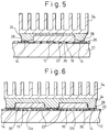
- Fig. 9 shows further embodiment of a semiconductor chip mounting structure according to the present invention.
- a semiconductor element 112 is mounted onto one surface (mounting surface) of a film type circuit board 110 at a position of a device hole provided thereon, and inner leads 120 of the circuit board, provided to project into the device hole as a circuit board side connecting section, are electrically connected to gold bumps 122 provided, as an element side connecting section, on a surface of the semiconductor element 12 opposite to the mounting surface.
- the joint portion between the circuit board side connecting section and the element side connecting section is sealed with an insulating resin layer 114.
- the other surface of the semiconductor element 112 is exposed from the insulating resin layer 114.
- connection between the circuit board side connecting section and the element side connecting section is made by connecting the inner lead 120 to the gold bump 122 formed on one surface of the semiconductor element 112, which inner lead projects into the device hole while forming part of conductor patterns 118 on one surface of a flexible film 116 constituting the circuit board 110.
- solder balls (solder bumps) 126 are connected to the conductor patterns 118 through via holes 128 penetrating the flexible film 116.
- the conductor patterns 118 are coated, except for the inner leads 120, with an insulating resin film 124 formed of an insulating resin such as silicone resin, and a metal layer 130 is provided on the surface of the resin film 124 in the peripheral area of the device hole, in which the semiconductor element 112 is carried, by a metallic foil such as copper or by a plating.
- an insulating resin film 124 formed of an insulating resin such as silicone resin
- a metal layer 130 is provided on the surface of the resin film 124 in the peripheral area of the device hole, in which the semiconductor element 112 is carried, by a metallic foil such as copper or by a plating.
- a TAB tape may be used, wherein the semiconductor element can be mounted on one ends of the conductor patterns 118 formed on one surface of a flexible film.
- the insulating resin for forming the insulating resin layer 114 those conventionally used for sealing semiconductor elements can be adopted, such as an epoxy type.
- an insulating inorganic substance such as silicon dioxide (SiO 2 ) is mixed as a filler so that the heat conductivity of the insulating resin layer 24 is improved.
- the film type circuit board 110 used in the embodiment shown in Figs. 9 through 11 has the circuit patterns 118 on one surface (on which the semiconductor element 112 is mounted) of the flexible film 116
- the circuit patterns 118 may be provided on the other surface (opposite to the surface on which the semiconductor element 112 is mounted).
- the external terminals such as solder bumps are attached by forming via-holes in a layer of resin such as silicone resin covering the conductor patterns 118 provided on the other surface of the flexible film 116 so that the conductor patterns 118 are exposed on the bottom thereof, and inserting the solder bumps into the via-holes.
- the heat dissipation ability of the semiconductor device is further enhanced by mounting a heat radiation fin 134 as shown in Fig. 12 on the outer surface of the low melting point metal layer 134 shown in Figs. 9 through 11.
- a heat spreader or a water-cooled channel may be used as means for dissipating heat.
- the electric property of the semiconductor device can be more improved by connecting a metal layer 130 in contact with a low melting point metal layer 134 to a solder ball 127 through a via-holes 129 penetrating a flexible film 116 and a resin film 124 so that the solder ball 127 is connected to a grounding pattern on the circuit board.
- a so-called area TAB tape may be used as the TAB tape for constituting the film type circuit board 110, wherein conductor patterns to be connected to the solder bumps 122 on the semiconductor element 112 are formed on a common surface of the flexible film 116, as shown in Fig. 13.
- a so-called dual metal type TAB tape may be used as the above-mentioned area TAB tape, wherein conductor patterns are formed not only on one surface of the flexible film 116 on which the semiconductor element 112 is to be mounted, but also on the other surface thereof, as shown in Fig. 14.
- a heat spreader 156 may be provided on the outer surface of the low melting point metal layer 134, as shown in Fig. 15, or a heat radiation fin 158 may be provided, as shown in Fig. 16.
- the area TAB tape 160 has conductor patterns 118, each of which is formed on one surface of a flexible film and has a mounting pad to be connected to a gold bump 122 of the semiconductor element 112.
- the tape is insulated from outside by a resin layer 124 formed, for example, of polyimide resin, except for an area wherein the semiconductor element 112 is mounted and the outer leads 154.
- the TAB tape is used, in the embodiment shown in Figs. 9 and 10, as a semiconductor element-mounting film having film side connecting sections provided on one surface of a flexible film 116 for the electric connection with element side connecting sections provided on one surface of the semiconductor element 112 to be mounted.
- the TAB tape usable for this purpose preferably has such a structure that a metal layer 130 is formed, as a layer capable of being closely bonded with the low melting point metal layer 134, at the periphery of a semiconductor element-mounting zone on a surface in contact with a low melting point metal layer 114 coating the mounted semiconductor element 110.
- Such a metal layer 134 can be provided by adhering a metallic foil or plating a metal such as copper on the surface of the flexible film 116 of the TAB tape or the surface of a resin layer 124 formed of an insulating resin such as silicone resin for partly insulating the conductive patterns 118.
- Polyimide resin was coated on a surface of a circuit board 10 made of alumina to form an insulating resin film 26, except for connection pads 16 of circuit patterns 14.
- a chromium layer has been formed on the resin film 26 by a sputtering
- a copper layer, a nickel layer and a gold layer were sequentially provided by a plating on the chromium layer so that a metal layer 28 (wettability improvement layer) having an uppermost gold layer was formed.
- connection terminals 18 provided on one surface of the semiconductor element 12 opposite to the circuit board were connected to the inner leads of the conductor patterns 20.
- connection terminals 18 of the semiconductor element 12 mounted onto the circuit board 10 and the connection pads 16 of the circuit patterns 14 were sealed with bisphenolic type epoxy resin containing silicon dioxide (SiO 2 ) filled in a gap between the one surface of the semiconductor element 12 and the mounting surface of the circuit board 10.
- the other surface (back surface) of the semiconductor element 12 was exposed from the thus-formed insulating resin layer 22 of epoxy resin.
- the insulating resin surface 22 was cured in a heated atmosphere to form a metallic powder layer 30 formed of the copper powder bonded to the surface of the insulating resin layer 22.
- solder paste contains a tungsten powder (of about 65% by weight) having a particle size of 80 to 100 mesh, each particle thereof having a surface layer of nickel provided through an electroless plating, and a rosin type flux added to improve the wettability to the tungsten powder.
- the circuit 10 After placing a heat radiation fin 34 of aluminum having a nickel/gold plated layer on a surface to be in contact with the solder paste (back surface), the circuit 10 was loaded as a whole into a reflow furnace to be subjected to a reflow treatment at 250°C for 30 seconds.
- the semiconductor device removed from the reflow furnace had a compact low melting point metal layer 24 formed of the solder, completely coating the semiconductor element 12 and the insulating resin layer 22, and the heat radiation fin 34 bonded thereto.
- a metal layer 28 was formed in the peripheral area on the surface of a circuit board 10 made of BT resin on which a semiconductor element 12 is to be mounted, which metal layer is formed of a copper foil connected via a through-hole to an earthing layer provided in the circuit board 10. Thereafter, a nickel-gold plated layer was formed on circuit patterns 14 provided on the surface of the circuit board.
- a bisphenolic type epoxy resin containing silicon dioxide (SiO 2 ) was filled in a gap between the one surface of the semiconductor element 12 and the mounting surface of the circuit board 10 to seal the joint portions between the solder bumps 36 and the connection pads 16 of the circuit patterns 14.
- the other surface (back surface) of the semiconductor element 12 was exposed outside an insulating resin layer 22 thus formed by the epoxy resin.
- the insulating resin surface 22 was cured in a heated atmosphere to form a metallic powder layer 30 formed of the copper powder bonded to the surface of the insulating resin layer 22.
- solder paste contains a tungsten powder (of about 65% by weight) having a particle size of 80 to 100 mesh, each particle thereof having a surface layer of nickel provided through an electroless plating, and a rosin type flux added to improve the wettability of the tungsten powder.
- the circuit 10 After placing a heat radiation fin 34 of aluminum having a nickel/gold plated layer on a surface to be in contact with the solder paste (back surface), the circuit 10 was loaded as a whole into a reflow furnace to be subjected to a reflow treatment at 250°C for 30 seconds.
- the semiconductor device removed from the reflow furnace had a compact low melting point metal layer 24 formed of the solder, completely coating the semiconductor element 12 and the insulating resin layer 22, and the heat radiation fin 34 bonded thereto.
- a TAB tape formed of a flexible film 116 of polyimide resin was used, on one surface of which are formed conductor patterns 118 so that inner leads 120 thereof project into a device hole provided on the flexible film 116.
- terminal pads are formed for providing bumps (solder balls) for the connection with a mounted circuit board (not shown).
- An insulating resin film 124 was formed all over one surface of the TAB tape, except for the device hole, by screen-printing a silicon type elastomer paste. Thereafter, a 70 ⁇ m thick copper foil was placed on the insulating resin layer 124. The TAB tape was cured to form a metal layer 130 bonded to the insulating resin film 124. The curing was conducted at 150°C for 2 hours.
- Electrodes provided on one surface of a semiconductor element 112 of 15 mm square were connected to the inner leads 120 of the TAB tape thus formed by a single bonding method.
- this semiconductor element 112 had a metalized layer of gold on the other surface thereof.
- joint portions between the TAB tape and the semiconductor element 112 were sealed with an insulating resin layer 114 formed of a silicon type potting agent.
- an insulating resin layer 114 formed of a silicon type potting agent.
- the insulating layer 114 was cured in a dry nitrogen atmosphere at 150°C for one hour to form a metallic powder layer 136 bonded onto the insulating resin layer 114.
- the back surface of the semiconductor element 112 was exposed from the insulating resin layer 114.
- a solder paste layer was formed on the back surface of the semiconductor element 112 mounted to the TAB tape by coating an eutectic Sn-Pb type solder paste containing a tungsten powder at 65% by weight, having a particle size of 80 to 100 mesh, each particle thereof having a surface layer of nickel provided through an electroless plating, and a heat radiation fin of aluminum alloy was placed on the solder paste layer, which fin has a gold film, provided by sputtering, on the bottom surface.
- a flux was coated on the terminal pads while disposing the flexible film 116 on the upper side, and solder balls of eutectic Sn-Pb type were arranged on the terminal pads. After being dried, the assembly was subjected to a reflow treatment in a dry nitrogen atmosphere at 250°C for one minute.
- the semiconductor device resulted from the reflow treatment was of a type shown in Fig. 12, wherein the low melting point metal layer 134 covering the semiconductor element 112 and the insulating resin layer 114 is closely bonded to the semiconductor element 112, the insulating resin layer 114 and the resin film 124 via the metalized layer of gold provided on the other surface of the semiconductor element 112, the metallic powder layer 136 on the insulating resin layer 114 and the metal layer 130 adhered to the resin film 124. It was confirmed from the heat cycle test or other that the durability and the heat dissipation ability of the resultant semiconductor device are favorable.
- An area TAB tape formed of a flexible film 116 of polyimide resin was used, on one surface of which were formed conductor patterns 118, each having a pad for the connection with a solder bump 122 on a semiconductor element 112.
- terminal pads were formed for providing bumps (solder balls) for the connection with a mounted circuit board.
- An insulating resin film 124 was formed all over one surface of the TAB tape, except for an area on which the semiconductor element 112 is to be mounted, by coating an epoxy type prepreg. Thereafter, a 35 ⁇ m thick copper foil was placed on the insulating resin film 124 and heat-pressed to form a metal layer 130 bonded to the insulating resin film 124. The heat-pressing was conducted at 180°C under the pressure of 30 kg/cm 2 .
- the 15 mm square semiconductor element 112 was mounted onto the mounting surface of the area TAB tape thus obtained by a flip chip bonding method wherein solder bumps 122 formed on one surface of the semiconductor element 112 are directly connected to the conductor patterns provided on the mounting surface of the area TAB tape.
- this semiconductor element 112 had a metalized layer of nickel/gold on the other surface thereof.
- joint portions between the area TAB tape and the semiconductor element 112 were sealed with an insulating resin layer 114 formed of an epoxy type potting agent.
- an insulating resin layer 114 formed of an epoxy type potting agent.
- the insulating layer 114 was cured in a dry nitrogen atmosphere at 150°C for one hour to form a metallic powder layer 136 bonded onto the insulating resin layer 114.
- the back surface of the semiconductor element 112 was exposed outside the insulating resin layer 114.
- a solder paste layer was formed on the back surface of the semiconductor element 112 mounted to the area TAB tape by coating an eutectic Sn-Pb type solder paste containing a copper powder of 50% by weight, having a particle size of 100 mesh, and a heat radiation fin of aluminum alloy was placed on the solder paste layer, which fin has a nickel/gold film, provided by a sputtering, on the bottom surface.
- a flux was coated on the terminal pads while disposing the flexible film 116 on the upper side, and solder balls of eutectic Sn-Pb type were arranged on the terminal pads. After being dried, the assembly was subjected to a reflow treatment in a dry nitrogen atmosphere at 230°C for one minute.
- the semiconductor device resulting from the reflow treatment was of a type shown in Fig. 13, wherein the low melting point metal layer 134 covering the semiconductor element 112 and the insulating resin layer 114 is closely bonded to the semiconductor element 112, the insulating resin layer 114 and the resin film 124 via the metalized layer of nickel/gold provided on the other surface of the semiconductor element 112, the metallic powder layer 136 on the insulating resin layer 114 and the metal layer 130 adhered to the resin layer 124. It was confirmed from the heat cycle test or other that the durability and the heat dissipation ability of the resultant semiconductor device are favorable.
- a TAB tape formed of a flexible film 116 of polyimide resin having a thickness of 75 ⁇ m was used, wherein conductor patterns 118 of a copper foil having a thickness of 25 ⁇ m are formed on one surface thereof, and each of the conductor patterns has an inner lead 120 projecting into a device hole of an annular square shape provided in a central area of the flexible film 116 and an outer lead 154 projecting outside from the periphery of the flexible film 116.
- an annular square-shaped copper foil having a thickness of 25 ⁇ m was adhered on the other surface of the TAB tape, which was then plated with gold to form a metal layer 30.
- a solder paste layer was formed on the back surface of the semiconductor element 112 mounted to the area TAB tape by coating an eutectic Sn-Pb type solder paste containing a copper powder at 50% by weight, having a particle size of 100 mesh, and a heat radiation fin of aluminum alloy was placed on the solder paste layer, which fin has a nickel/gold film provided by sputtering on the bottom surface.
- a flux was coated on the terminal pads while disposing the flexible film 116 on the upper side, and solder balls of eutectic Sn-Pb type were arranged on the terminal pads. After being dried, the assembly was subjected to a reflow treatment in a dry nitrogen atmosphere at 230°C for one minute.
- the semiconductor device resulting from the reflow treatment was of a type shown in Fig. 16, wherein the low melting point metal layer 134 covering the semiconductor element 112 and the insulating resin layer 114 is closely bonded to the semiconductor element 112, the insulating resin layer 114 and the flexible film 116 via the metalized layer of nickel/gold provided on the other surface of the semiconductor element 112, the metallic powder layer 136 on the insulating resin layer 114 and the metal layer 130 adhered to the resin layer 124. It was confirmed from the heat cycle test or others that the durability and the heat dissipation ability of the resultant semiconductor device are favorable.
- An area TAB tape formed of a flexible film 116 of polyimide resin having a thickness of 35 ⁇ m was used, wherein conductor patterns to be connected to solder bumps 122 provided, as connection terminals, on one surface of a semiconductor element 112 are formed on the same surface as conductor patterns 118 of the flexible film 116.
- a 35 ⁇ m thick annular square-shaped copper foil was placed on the periphery of an area of the area TAB tape element 112 (on the surface on which the conductor patterns 118 are provided) for mounting the semiconductor element 112, via a resin film 124 formed of a 60 ⁇ m thick epoxy type prepreg layer. Thereafter, the copper foil was bonded to the resin layer 124 by a heat-pressing to form a metal layer 130. The heat-pressing was conducted at 180°C under a pressure of 30 kg/cm 2 .
- the 11 mm square semiconductor element 112 was mounted onto the mounting area of the area TAB tape by a flip-chip bonding method wherein solder bumps 122 provided on one surface of the semiconductor element 112 are directly connected to the conductor patterns formed on the mounting surface of the area TAB tape.
- the joint portions between the area TAB tape and the semiconductor element 112 were sealed with an insulating resin layer 114 formed of a solvent type potting agent of a bisphenolic epoxy type. Then, after a copper powder was spread on the surface of the insulating resin layer 114, the insulating resin layer 114 was cured in a dry nitrogen atmosphere at 150°C for one hour so that the copper powder closely adhered to the insulating resin layer 114 to form a metallic powder layer 136. In this regard, the back surface of the semiconductor element 112 was exposed outside the insulating resin layer 114.
- a solder paste layer was formed on the back surface of the semiconductor element 112 mounted to the area TAB tape by coating an eutectic Sn-Pb type solder paste containing a tungsten powder at 60% by weight, having a particle size of 80 to 100 mesh, each particle thereof having a surface layer of nickel provided through electroless plating, and a heat radiation fin of aluminum alloy was placed on the solder paste layer, which fin has a nickel/gold film provided by a sputtering on the bottom surface.
- the area TAB tape carrying the semiconductor element 112 thereon was subjected to a reflow treatment in a dry nitrogen atmosphere at 230°C for one minute.
- the semiconductor device resulting from the reflow treatment was of a type, shown in Fig. 17, wherein the low melting point metal layer 134 covering the semiconductor element 112 and the insulating resin layer 114 is closely bonded to the semiconductor element 112, the insulating resin layer 114 and the resin film 124 via the metalized layer of nickel/gold provided on the other surface of the semiconductor element 112, the metallic powder layer 136 on the insulating resin layer 114 and the metal layer 130 adhered to the resin layer 124. It was confirmed from the heat cycle test or other that the durability and the heat dissipation ability of the resultant semiconductor device are favorable.
Applications Claiming Priority (6)
| Application Number | Priority Date | Filing Date | Title |
|---|---|---|---|
| JP8238595 | 1995-04-07 | ||
| JP7082385A JPH08279576A (ja) | 1995-04-07 | 1995-04-07 | 半導体素子の実装構造体及び半導体素子の実装方法 |
| JP82385/95 | 1995-04-07 | ||
| JP8367995 | 1995-04-10 | ||
| JP83679/95 | 1995-04-10 | ||
| JP7083679A JPH08279533A (ja) | 1995-04-10 | 1995-04-10 | 半導体装置及び半導体素子搭載用フィルム |
Publications (3)
| Publication Number | Publication Date |
|---|---|
| EP0740340A2 true EP0740340A2 (de) | 1996-10-30 |
| EP0740340A3 EP0740340A3 (de) | 1997-10-29 |
| EP0740340B1 EP0740340B1 (de) | 2002-06-26 |
Family
ID=26423418
Family Applications (1)
| Application Number | Title | Priority Date | Filing Date |
|---|---|---|---|
| EP96302414A Expired - Lifetime EP0740340B1 (de) | 1995-04-07 | 1996-04-04 | Struktur und Verfahren zur Montage eines Halbleiterchips |
Country Status (3)
| Country | Link |
|---|---|
| US (1) | US5737191A (de) |
| EP (1) | EP0740340B1 (de) |
| DE (1) | DE69621983T2 (de) |
Cited By (9)
| Publication number | Priority date | Publication date | Assignee | Title |
|---|---|---|---|---|
| WO1998024121A1 (de) * | 1996-11-29 | 1998-06-04 | Siemens Aktiengesellschaft | Halbleiterchip und wafer mit schutzschicht, insbesondere aus keramik |
| EP1061574A1 (de) * | 1999-06-17 | 2000-12-20 | Ming-Tung Shen | Halbleiteranordnung und Herstellungsverfahren dafür |
| EP1065718A1 (de) * | 1999-06-17 | 2001-01-03 | Ming-Tung Shen | Halbleiterchipmodul und Herstellungsverfahren dafür |
| EP1075024A2 (de) * | 1999-08-03 | 2001-02-07 | Shinko Electric Industries Co. Ltd. | Chipträger mit fasriger Kühlplatte |
| US6278183B1 (en) | 1999-04-16 | 2001-08-21 | Ming-Tung Shen | Semiconductor device and method for manufacturing the same |
| DE10107399A1 (de) * | 2001-02-14 | 2002-09-12 | Infineon Technologies Ag | Elektronisches Bauteil mit Kantenschutz |
| WO2003058812A1 (de) * | 2001-12-28 | 2003-07-17 | Epcos Ag | Verfahren zur hermetischen verkapselung eines bauelements |
| WO2005006433A2 (en) * | 2003-06-30 | 2005-01-20 | Intel Corporation | Mold compound cap in a flip chip multi-matrix array package and process of making same |
| US11244876B2 (en) | 2019-10-09 | 2022-02-08 | Microchip Technology Inc. | Packaged semiconductor die with micro-cavity |
Families Citing this family (84)
| Publication number | Priority date | Publication date | Assignee | Title |
|---|---|---|---|---|
| JPH09260533A (ja) | 1996-03-19 | 1997-10-03 | Hitachi Ltd | 半導体装置及びその実装構造 |
| US5928568A (en) * | 1996-06-24 | 1999-07-27 | Delco Electonics Corporation | Thick film circuit having conductor composition with coated metallic particles |
| JPH1032275A (ja) * | 1996-07-13 | 1998-02-03 | Ricoh Co Ltd | 半導体装置およびその製造方法 |
| JP3431406B2 (ja) * | 1996-07-30 | 2003-07-28 | 株式会社東芝 | 半導体パッケージ装置 |
| US6011694A (en) * | 1996-08-01 | 2000-01-04 | Fuji Machinery Mfg. & Electronics Co., Ltd. | Ball grid array semiconductor package with solder ball openings in an insulative base |
| US6962829B2 (en) * | 1996-10-31 | 2005-11-08 | Amkor Technology, Inc. | Method of making near chip size integrated circuit package |
| JP2933554B2 (ja) * | 1996-11-28 | 1999-08-16 | 九州日本電気株式会社 | 半導体装置およびその製造方法 |
| JP3695893B2 (ja) * | 1996-12-03 | 2005-09-14 | 沖電気工業株式会社 | 半導体装置とその製造方法および実装方法 |
| US6020221A (en) * | 1996-12-12 | 2000-02-01 | Lsi Logic Corporation | Process for manufacturing a semiconductor device having a stiffener member |
| KR100246333B1 (ko) * | 1997-03-14 | 2000-03-15 | 김영환 | 비 지 에이 패키지 및 그 제조방법 |
| US6084777A (en) * | 1997-04-23 | 2000-07-04 | Texas Instruments Incorporated | Ball grid array package |
| US5866943A (en) * | 1997-06-23 | 1999-02-02 | Lsi Logic Corporation | System and method for forming a grid array device package employing electomagnetic shielding |
| US6002171A (en) * | 1997-09-22 | 1999-12-14 | Lsi Logic Corporation | Integrated heat spreader/stiffener assembly and method of assembly for semiconductor package |
| US6166434A (en) * | 1997-09-23 | 2000-12-26 | Lsi Logic Corporation | Die clip assembly for semiconductor package |
| US5909057A (en) * | 1997-09-23 | 1999-06-01 | Lsi Logic Corporation | Integrated heat spreader/stiffener with apertures for semiconductor package |
| US6172413B1 (en) * | 1997-10-09 | 2001-01-09 | Micron Technology, Inc. | Chip leads constrained in dielectric media |
| US5965944A (en) * | 1997-11-12 | 1999-10-12 | International Business Machines Corporation | Printed circuit boards for mounting a semiconductor integrated circuit die |
| US5942798A (en) | 1997-11-24 | 1999-08-24 | Stmicroelectronics, Inc. | Apparatus and method for automating the underfill of flip-chip devices |
| JP3367886B2 (ja) | 1998-01-20 | 2003-01-20 | 株式会社村田製作所 | 電子回路装置 |
| KR19990068199A (ko) * | 1998-01-30 | 1999-08-25 | 모기 쥰이찌 | 프레임 형상의 몰드부를 갖는 반도체 장치용 패키지 및 그 제조 방법 |
| JP3481117B2 (ja) * | 1998-02-25 | 2003-12-22 | 富士通株式会社 | 半導体装置及びその製造方法 |
| EP0942392A3 (de) * | 1998-03-13 | 2000-10-18 | Kabushiki Kaisha Toshiba | Chipkarte |
| US6191487B1 (en) * | 1998-04-23 | 2001-02-20 | Minco Technology Labs, Inc. | Semiconductor and flip chip packages and method having a back-side connection |
| KR100277438B1 (ko) * | 1998-05-28 | 2001-02-01 | 윤종용 | 멀티칩패키지 |
| US6404067B1 (en) | 1998-06-01 | 2002-06-11 | Intel Corporation | Plastic ball grid array package with improved moisture resistance |
| US6081037A (en) * | 1998-06-22 | 2000-06-27 | Motorola, Inc. | Semiconductor component having a semiconductor chip mounted to a chip mount |
| JP2000100985A (ja) * | 1998-09-17 | 2000-04-07 | Nitto Denko Corp | 半導体素子実装用基板およびその製造方法と用途 |
| US6248951B1 (en) * | 1999-01-05 | 2001-06-19 | Intel Corporation | Dielectric decal for a substrate of an integrated circuit package |
| WO2000070670A1 (en) * | 1999-05-12 | 2000-11-23 | Hitachi, Ltd. | Semiconductor device and method for manufacturing the same, and electronic device |
| US6594156B1 (en) * | 2000-04-24 | 2003-07-15 | Minimed Inc. | Device and method for circuit protection during radiation sterilization |
| TW561799B (en) * | 1999-08-11 | 2003-11-11 | Fujikura Ltd | Chip assembly module of bump connection type using a multi-layer printed circuit substrate |
| JP2001077301A (ja) * | 1999-08-24 | 2001-03-23 | Amkor Technology Korea Inc | 半導体パッケージ及びその製造方法 |
| US6281437B1 (en) | 1999-11-10 | 2001-08-28 | International Business Machines Corporation | Method of forming an electrical connection between a conductive member having a dual thickness substrate and a conductor and electronic package including said connection |
| JP2001291802A (ja) * | 2000-04-06 | 2001-10-19 | Shinko Electric Ind Co Ltd | 配線基板及びその製造方法ならびに半導体装置 |
| JP2002033411A (ja) * | 2000-07-13 | 2002-01-31 | Nec Corp | ヒートスプレッダ付き半導体装置及びその製造方法 |
| EP1263043A1 (de) * | 2001-05-30 | 2002-12-04 | Alcatel | Elektronisches Element mit Abschirmung |
| KR100431180B1 (ko) * | 2001-12-07 | 2004-05-12 | 삼성전기주식회사 | 표면 탄성파 필터 패키지 제조방법 |
| US6617524B2 (en) * | 2001-12-11 | 2003-09-09 | Motorola, Inc. | Packaged integrated circuit and method therefor |
| JP2003298220A (ja) * | 2002-03-29 | 2003-10-17 | Hitachi Ltd | 回路基板および電子機器、およびそれらの製造方法 |
| JP4357817B2 (ja) * | 2002-09-12 | 2009-11-04 | パナソニック株式会社 | 回路部品内蔵モジュール |
| US20070164424A1 (en) * | 2003-04-02 | 2007-07-19 | Nancy Dean | Thermal interconnect and interface systems, methods of production and uses thereof |
| US20050247761A1 (en) * | 2004-05-04 | 2005-11-10 | Albanese Patricia M | Surface mount attachment of components |
| WO2004109795A2 (en) * | 2003-06-06 | 2004-12-16 | Honeywell International Inc. | Thermal interconnect system and method of production thereof |
| DE10329329B4 (de) * | 2003-06-30 | 2005-08-18 | Siemens Ag | Hochfrequenz-Gehäuse und Verfahren zu seiner Herstellung |
| TWI228804B (en) * | 2003-07-02 | 2005-03-01 | Lite On Semiconductor Corp | Chip package substrate having flexible printed circuit board and method for fabricating the same |
| US20050056458A1 (en) * | 2003-07-02 | 2005-03-17 | Tsuyoshi Sugiura | Mounting pad, package, device, and method of fabricating the device |
| JP3811160B2 (ja) * | 2004-03-09 | 2006-08-16 | 株式会社東芝 | 半導体装置 |
| US7160758B2 (en) * | 2004-03-31 | 2007-01-09 | Intel Corporation | Electronic packaging apparatus and method |
| KR20060001352A (ko) * | 2004-06-30 | 2006-01-06 | 삼성에스디아이 주식회사 | 플라즈마 디스플레이 패널 |
| US7183657B2 (en) * | 2004-09-23 | 2007-02-27 | Texas Instruments Incorporated | Semiconductor device having resin anti-bleed feature |
| KR100608610B1 (ko) * | 2004-12-20 | 2006-08-08 | 삼성전자주식회사 | 인쇄회로기판과, 그의 제조 방법 및 그를 이용한 반도체패키지 |
| TW200631144A (en) * | 2005-02-18 | 2006-09-01 | Mitac Technology Corp | Chip heat dissipation structure and manufacturing method thereof |
| JP4860994B2 (ja) * | 2005-12-06 | 2012-01-25 | ルネサスエレクトロニクス株式会社 | 半導体装置 |
| US7485502B2 (en) * | 2006-01-31 | 2009-02-03 | Stats Chippac Ltd. | Integrated circuit underfill package system |
| TWI300679B (en) * | 2006-02-22 | 2008-09-01 | Au Optronics Corp | Assembly of fpc and electric component |
| WO2008115744A1 (en) * | 2007-03-16 | 2008-09-25 | Vertical Circuits, Inc. | Vertical electrical interconnect formed on support prior to die mount |
| US8723332B2 (en) * | 2007-06-11 | 2014-05-13 | Invensas Corporation | Electrically interconnected stacked die assemblies |
| FR2919426B1 (fr) * | 2007-07-23 | 2009-12-11 | Commissariat Energie Atomique | Procede d'enrobage de deux elements hybrides entre eux au moyen d'un materiau de brasure |
| US8704379B2 (en) | 2007-09-10 | 2014-04-22 | Invensas Corporation | Semiconductor die mount by conformal die coating |
| JP2009081279A (ja) * | 2007-09-26 | 2009-04-16 | Sanyo Electric Co Ltd | 混成集積回路装置 |
| US20090091021A1 (en) * | 2007-10-03 | 2009-04-09 | Matsushita Electric Industrial Co., Ltd. | Semiconductor device and method of manufacturing the same |
| US7906860B2 (en) * | 2007-10-26 | 2011-03-15 | Infineon Technologies Ag | Semiconductor device |
| US9147665B2 (en) * | 2007-11-06 | 2015-09-29 | Fairchild Semiconductor Corporation | High bond line thickness for semiconductor devices |
| WO2009114670A2 (en) | 2008-03-12 | 2009-09-17 | Vertical Circuits, Inc. | Support mounted electrically interconnected die assembly |
| US9153517B2 (en) | 2008-05-20 | 2015-10-06 | Invensas Corporation | Electrical connector between die pad and z-interconnect for stacked die assemblies |
| US7863159B2 (en) * | 2008-06-19 | 2011-01-04 | Vertical Circuits, Inc. | Semiconductor die separation method |
| TWI570879B (zh) * | 2009-06-26 | 2017-02-11 | 英維瑟斯公司 | 半導體總成及晶粒堆疊總成 |
| US9433105B2 (en) * | 2009-08-25 | 2016-08-30 | International Business Machines Corporation | Method of fabricating printed circuit boards |
| US9147583B2 (en) | 2009-10-27 | 2015-09-29 | Invensas Corporation | Selective die electrical insulation by additive process |
| TWI544604B (zh) | 2009-11-04 | 2016-08-01 | 英維瑟斯公司 | 具有降低應力電互連的堆疊晶粒總成 |
| US8299633B2 (en) * | 2009-12-21 | 2012-10-30 | Advanced Micro Devices, Inc. | Semiconductor chip device with solder diffusion protection |
| US8193040B2 (en) * | 2010-02-08 | 2012-06-05 | Infineon Technologies Ag | Manufacturing of a device including a semiconductor chip |
| KR101067216B1 (ko) * | 2010-05-24 | 2011-09-22 | 삼성전기주식회사 | 인쇄회로기판 및 이를 구비하는 반도체 패키지 |
| DE102011003195B4 (de) * | 2011-01-26 | 2019-01-10 | Robert Bosch Gmbh | Bauteil und Verfahren zum Herstellen eines Bauteils |
| US9658000B2 (en) | 2012-02-15 | 2017-05-23 | Abaco Systems, Inc. | Flexible metallic heat connector |
| JP5725055B2 (ja) * | 2013-02-12 | 2015-05-27 | 株式会社デンソー | 電子制御ユニット |
| US9490195B1 (en) | 2015-07-17 | 2016-11-08 | Invensas Corporation | Wafer-level flipped die stacks with leadframes or metal foil interconnects |
| US9825002B2 (en) | 2015-07-17 | 2017-11-21 | Invensas Corporation | Flipped die stack |
| US9871019B2 (en) | 2015-07-17 | 2018-01-16 | Invensas Corporation | Flipped die stack assemblies with leadframe interconnects |
| US9508691B1 (en) | 2015-12-16 | 2016-11-29 | Invensas Corporation | Flipped die stacks with multiple rows of leadframe interconnects |
| US10566310B2 (en) | 2016-04-11 | 2020-02-18 | Invensas Corporation | Microelectronic packages having stacked die and wire bond interconnects |
| US9595511B1 (en) | 2016-05-12 | 2017-03-14 | Invensas Corporation | Microelectronic packages and assemblies with improved flyby signaling operation |
| US9728524B1 (en) | 2016-06-30 | 2017-08-08 | Invensas Corporation | Enhanced density assembly having microelectronic packages mounted at substantial angle to board |
| US11152274B2 (en) * | 2017-09-11 | 2021-10-19 | Advanced Semiconductor Engineering, Inc. | Multi-moldings fan-out package and process |
Citations (9)
| Publication number | Priority date | Publication date | Assignee | Title |
|---|---|---|---|---|
| US4323914A (en) * | 1979-02-01 | 1982-04-06 | International Business Machines Corporation | Heat transfer structure for integrated circuit package |
| JPH0196952A (ja) * | 1987-10-09 | 1989-04-14 | Hitachi Ltd | 気密封止チツプキヤリア |
| JPH02288255A (ja) * | 1989-04-28 | 1990-11-28 | Hitachi Ltd | 半導体装置 |
| JPH0432251A (ja) * | 1990-05-29 | 1992-02-04 | Hitachi Ltd | 半導体パッケージ及びその製造方法 |
| US5107325A (en) * | 1989-04-17 | 1992-04-21 | Seiko Epson Corporation | Structure and method of packaging a semiconductor device |
| JPH04122053A (ja) * | 1990-09-12 | 1992-04-22 | Fujitsu Ltd | 半導体チップの実装方法 |
| JPH0582584A (ja) * | 1991-09-19 | 1993-04-02 | Nec Corp | 半導体装置 |
| JPH0661383A (ja) * | 1992-08-11 | 1994-03-04 | Fujitsu Ltd | 半導体装置 |
| EP0603928A1 (de) * | 1992-12-21 | 1994-06-29 | Delco Electronics Corporation | Hybridschaltung |
Family Cites Families (1)
| Publication number | Priority date | Publication date | Assignee | Title |
|---|---|---|---|---|
| JPS53144220A (en) * | 1977-05-23 | 1978-12-15 | Hitachi Ltd | Automatic adjuster for color purity of color television |
-
1996
- 1996-04-04 DE DE69621983T patent/DE69621983T2/de not_active Expired - Fee Related
- 1996-04-04 EP EP96302414A patent/EP0740340B1/de not_active Expired - Lifetime
- 1996-04-05 US US08/628,346 patent/US5737191A/en not_active Expired - Fee Related
Patent Citations (9)
| Publication number | Priority date | Publication date | Assignee | Title |
|---|---|---|---|---|
| US4323914A (en) * | 1979-02-01 | 1982-04-06 | International Business Machines Corporation | Heat transfer structure for integrated circuit package |
| JPH0196952A (ja) * | 1987-10-09 | 1989-04-14 | Hitachi Ltd | 気密封止チツプキヤリア |
| US5107325A (en) * | 1989-04-17 | 1992-04-21 | Seiko Epson Corporation | Structure and method of packaging a semiconductor device |
| JPH02288255A (ja) * | 1989-04-28 | 1990-11-28 | Hitachi Ltd | 半導体装置 |
| JPH0432251A (ja) * | 1990-05-29 | 1992-02-04 | Hitachi Ltd | 半導体パッケージ及びその製造方法 |
| JPH04122053A (ja) * | 1990-09-12 | 1992-04-22 | Fujitsu Ltd | 半導体チップの実装方法 |
| JPH0582584A (ja) * | 1991-09-19 | 1993-04-02 | Nec Corp | 半導体装置 |
| JPH0661383A (ja) * | 1992-08-11 | 1994-03-04 | Fujitsu Ltd | 半導体装置 |
| EP0603928A1 (de) * | 1992-12-21 | 1994-06-29 | Delco Electronics Corporation | Hybridschaltung |
Non-Patent Citations (6)
| Title |
|---|
| PATENT ABSTRACTS OF JAPAN vol. 013, no. 333 (E-794), 26 July 1989 & JP 01 096952 A (HITACHI LTD), 14 April 1989, * |
| PATENT ABSTRACTS OF JAPAN vol. 015, no. 062 (E-1033), 14 February 1991 & JP 02 288255 A (HITACHI LTD), 28 November 1990, * |
| PATENT ABSTRACTS OF JAPAN vol. 016, no. 204 (E-1202), 15 May 1992 & JP 04 032251 A (HITACHI LTD;OTHERS: 01), 4 February 1992, * |
| PATENT ABSTRACTS OF JAPAN vol. 016, no. 381 (E-1248), 14 August 1992 & JP 04 122053 A (FUJITSU LTD), 22 April 1992, * |
| PATENT ABSTRACTS OF JAPAN vol. 017, no. 415 (E-1407), 3 August 1993 & JP 05 082584 A (NEC CORP), 2 April 1993, * |
| PATENT ABSTRACTS OF JAPAN vol. 018, no. 299 (E-1558), 8 June 1994 & JP 06 061383 A (FUJITSU LTD), 4 March 1994, * |
Cited By (19)
| Publication number | Priority date | Publication date | Assignee | Title |
|---|---|---|---|---|
| WO1998024121A1 (de) * | 1996-11-29 | 1998-06-04 | Siemens Aktiengesellschaft | Halbleiterchip und wafer mit schutzschicht, insbesondere aus keramik |
| US6278183B1 (en) | 1999-04-16 | 2001-08-21 | Ming-Tung Shen | Semiconductor device and method for manufacturing the same |
| US6420210B2 (en) | 1999-04-16 | 2002-07-16 | Computech International Ventures Limited | Semiconductor device and method for manufacturing the same |
| EP1061574A1 (de) * | 1999-06-17 | 2000-12-20 | Ming-Tung Shen | Halbleiteranordnung und Herstellungsverfahren dafür |
| EP1065718A1 (de) * | 1999-06-17 | 2001-01-03 | Ming-Tung Shen | Halbleiterchipmodul und Herstellungsverfahren dafür |
| EP1075024A2 (de) * | 1999-08-03 | 2001-02-07 | Shinko Electric Industries Co. Ltd. | Chipträger mit fasriger Kühlplatte |
| EP1075024A3 (de) * | 1999-08-03 | 2001-12-19 | Shinko Electric Industries Co. Ltd. | Chipträger mit fasriger Kühlplatte |
| US6404070B1 (en) | 1999-08-03 | 2002-06-11 | Shinko Electric Industries Co., Ltd. | Semiconductor device |
| DE10107399A1 (de) * | 2001-02-14 | 2002-09-12 | Infineon Technologies Ag | Elektronisches Bauteil mit Kantenschutz |
| WO2003058812A1 (de) * | 2001-12-28 | 2003-07-17 | Epcos Ag | Verfahren zur hermetischen verkapselung eines bauelements |
| US7259041B2 (en) | 2001-12-28 | 2007-08-21 | Epcos Ag | Method for the hermetic encapsulation of a component |
| WO2005006433A2 (en) * | 2003-06-30 | 2005-01-20 | Intel Corporation | Mold compound cap in a flip chip multi-matrix array package and process of making same |
| WO2005006433A3 (en) * | 2003-06-30 | 2005-03-24 | Intel Corp | Mold compound cap in a flip chip multi-matrix array package and process of making same |
| GB2434031A (en) * | 2003-06-30 | 2007-07-11 | Intel Corp | Mold compound cap in a flip chip multi-matrix array package and process of making same |
| US7294533B2 (en) | 2003-06-30 | 2007-11-13 | Intel Corporation | Mold compound cap in a flip chip multi-matrix array package and process of making same |
| GB2434031B (en) * | 2003-06-30 | 2008-04-09 | Intel Corp | Mold compound cap in a flip chip multi-matrix array package and process of making same |
| US7514300B2 (en) | 2003-06-30 | 2009-04-07 | Intel Corporation | Mold compound cap in a flip chip multi-matrix array package and process of making same |
| DE112004001131B4 (de) * | 2003-06-30 | 2016-12-01 | Intel Corporation | Preßmassenaufsatz in einem Flip-Chip Multi-Matrix Anordnungspaket und Verfahren zu dessen Herstellung |
| US11244876B2 (en) | 2019-10-09 | 2022-02-08 | Microchip Technology Inc. | Packaged semiconductor die with micro-cavity |
Also Published As
| Publication number | Publication date |
|---|---|
| EP0740340A3 (de) | 1997-10-29 |
| DE69621983T2 (de) | 2002-11-21 |
| DE69621983D1 (de) | 2002-08-01 |
| EP0740340B1 (de) | 2002-06-26 |
| US5737191A (en) | 1998-04-07 |
Similar Documents
| Publication | Publication Date | Title |
|---|---|---|
| EP0740340B1 (de) | Struktur und Verfahren zur Montage eines Halbleiterchips | |
| KR100231276B1 (ko) | 반도체패키지의 구조 및 제조방법 | |
| JP4051893B2 (ja) | 電子機器 | |
| JP3549294B2 (ja) | 半導体装置及びその実装構造 | |
| US6262477B1 (en) | Ball grid array electronic package | |
| KR100532179B1 (ko) | 집적 회로 패키지를 위한 칩 규모 볼 그리드 어레이 | |
| US6028357A (en) | Semiconductor device with a solder bump over a pillar form | |
| US5435732A (en) | Flexible circuit member | |
| EP0915505B1 (de) | Packung für eine Halbleiteranordnung, Verfahren zu ihrer Herstellung und Leiterplatte dafür | |
| JP3704864B2 (ja) | 半導体素子の実装構造 | |
| US7098072B2 (en) | Fluxless assembly of chip size semiconductor packages | |
| KR100442695B1 (ko) | 열 방출판이 부착된 플립칩 패키지 제조 방법 | |
| US20010048591A1 (en) | Microelectronics component with rigid interposer | |
| WO1997020347A1 (en) | Semiconductor device, process for producing the same, and packaged substrate | |
| JP2000323516A (ja) | 配線基板の製造方法及び配線基板及び半導体装置 | |
| JP3492025B2 (ja) | 回路基板構造 | |
| JP2003086626A (ja) | 電子部品、その製造方法、電子部品の実装体および実装方法 | |
| KR100206033B1 (ko) | 반도체소자의 실장구조체 및 반도체소자의 실장방법 | |
| KR100235091B1 (ko) | 반도체장치 및 반도체소자탑재용 필름 | |
| JPH10275522A (ja) | 導電性樹脂ペースト、それを用いたパッケージ用基体および半導体パッケージ | |
| WO2008021797A1 (en) | Thermally enhanced bga package apparatus and method | |
| JPS6395637A (ja) | 半導体集積回路装置 | |
| WO2003075337A1 (en) | Fluxless assembly of chip size semiconductor packages | |
| JP4071893B2 (ja) | 配線基板およびその実装構造 | |
| JP2000040776A (ja) | 半導体素子の実装構造 |
Legal Events
| Date | Code | Title | Description |
|---|---|---|---|
| PUAI | Public reference made under article 153(3) epc to a published international application that has entered the european phase |
Free format text: ORIGINAL CODE: 0009012 |
|
| AK | Designated contracting states |
Kind code of ref document: A2 Designated state(s): DE FR GB |
|
| PUAL | Search report despatched |
Free format text: ORIGINAL CODE: 0009013 |
|
| AK | Designated contracting states |
Kind code of ref document: A3 Designated state(s): DE FR GB |
|
| 17P | Request for examination filed |
Effective date: 19980417 |
|
| 17Q | First examination report despatched |
Effective date: 19991028 |
|
| GRAG | Despatch of communication of intention to grant |
Free format text: ORIGINAL CODE: EPIDOS AGRA |
|
| GRAG | Despatch of communication of intention to grant |
Free format text: ORIGINAL CODE: EPIDOS AGRA |
|
| GRAH | Despatch of communication of intention to grant a patent |
Free format text: ORIGINAL CODE: EPIDOS IGRA |
|
| GRAH | Despatch of communication of intention to grant a patent |
Free format text: ORIGINAL CODE: EPIDOS IGRA |
|
| GRAA | (expected) grant |
Free format text: ORIGINAL CODE: 0009210 |
|
| AK | Designated contracting states |
Kind code of ref document: B1 Designated state(s): DE FR GB |
|
| REG | Reference to a national code |
Ref country code: GB Ref legal event code: FG4D |
|
| REF | Corresponds to: |
Ref document number: 69621983 Country of ref document: DE Date of ref document: 20020801 |
|
| ET | Fr: translation filed | ||
| PLBE | No opposition filed within time limit |
Free format text: ORIGINAL CODE: 0009261 |
|
| STAA | Information on the status of an ep patent application or granted ep patent |
Free format text: STATUS: NO OPPOSITION FILED WITHIN TIME LIMIT |
|
| 26N | No opposition filed |
Effective date: 20030327 |
|
| PGFP | Annual fee paid to national office [announced via postgrant information from national office to epo] |
Ref country code: GB Payment date: 20050330 Year of fee payment: 10 |
|
| PGFP | Annual fee paid to national office [announced via postgrant information from national office to epo] |
Ref country code: DE Payment date: 20050331 Year of fee payment: 10 |
|
| PGFP | Annual fee paid to national office [announced via postgrant information from national office to epo] |
Ref country code: FR Payment date: 20050408 Year of fee payment: 10 |
|
| PG25 | Lapsed in a contracting state [announced via postgrant information from national office to epo] |
Ref country code: GB Free format text: LAPSE BECAUSE OF NON-PAYMENT OF DUE FEES Effective date: 20060404 |
|
| PG25 | Lapsed in a contracting state [announced via postgrant information from national office to epo] |
Ref country code: DE Free format text: LAPSE BECAUSE OF NON-PAYMENT OF DUE FEES Effective date: 20061101 |
|
| GBPC | Gb: european patent ceased through non-payment of renewal fee |
Effective date: 20060404 |
|
| REG | Reference to a national code |
Ref country code: FR Ref legal event code: ST Effective date: 20061230 |
|
| PG25 | Lapsed in a contracting state [announced via postgrant information from national office to epo] |
Ref country code: FR Free format text: LAPSE BECAUSE OF NON-PAYMENT OF DUE FEES Effective date: 20060502 |