EP0725980B1 - Herstellungsverfahren für einen ein eeprom und einen kondensator enthaltenden integrierten schaltungschip - Google Patents
Herstellungsverfahren für einen ein eeprom und einen kondensator enthaltenden integrierten schaltungschip Download PDFInfo
- Publication number
- EP0725980B1 EP0725980B1 EP95931647A EP95931647A EP0725980B1 EP 0725980 B1 EP0725980 B1 EP 0725980B1 EP 95931647 A EP95931647 A EP 95931647A EP 95931647 A EP95931647 A EP 95931647A EP 0725980 B1 EP0725980 B1 EP 0725980B1
- Authority
- EP
- European Patent Office
- Prior art keywords
- mask
- gate
- layer
- floating gate
- source
- Prior art date
- Legal status (The legal status is an assumption and is not a legal conclusion. Google has not performed a legal analysis and makes no representation as to the accuracy of the status listed.)
- Expired - Lifetime
Links
Images











Classifications
-
- H—ELECTRICITY
- H10—SEMICONDUCTOR DEVICES; ELECTRIC SOLID-STATE DEVICES NOT OTHERWISE PROVIDED FOR
- H10B—ELECTRONIC MEMORY DEVICES
- H10B41/00—Electrically erasable-and-programmable ROM [EEPROM] devices comprising floating gates
- H10B41/40—Electrically erasable-and-programmable ROM [EEPROM] devices comprising floating gates characterised by the peripheral circuit region
-
- H—ELECTRICITY
- H10—SEMICONDUCTOR DEVICES; ELECTRIC SOLID-STATE DEVICES NOT OTHERWISE PROVIDED FOR
- H10B—ELECTRONIC MEMORY DEVICES
- H10B41/00—Electrically erasable-and-programmable ROM [EEPROM] devices comprising floating gates
- H10B41/40—Electrically erasable-and-programmable ROM [EEPROM] devices comprising floating gates characterised by the peripheral circuit region
- H10B41/42—Simultaneous manufacture of periphery and memory cells
- H10B41/49—Simultaneous manufacture of periphery and memory cells comprising different types of peripheral transistor
-
- H—ELECTRICITY
- H10—SEMICONDUCTOR DEVICES; ELECTRIC SOLID-STATE DEVICES NOT OTHERWISE PROVIDED FOR
- H10B—ELECTRONIC MEMORY DEVICES
- H10B41/00—Electrically erasable-and-programmable ROM [EEPROM] devices comprising floating gates
- H10B41/20—Electrically erasable-and-programmable ROM [EEPROM] devices comprising floating gates characterised by three-dimensional [3D] arrangements, e.g. with cells on different height levels
-
- H—ELECTRICITY
- H10—SEMICONDUCTOR DEVICES; ELECTRIC SOLID-STATE DEVICES NOT OTHERWISE PROVIDED FOR
- H10B—ELECTRONIC MEMORY DEVICES
- H10B41/00—Electrically erasable-and-programmable ROM [EEPROM] devices comprising floating gates
- H10B41/40—Electrically erasable-and-programmable ROM [EEPROM] devices comprising floating gates characterised by the peripheral circuit region
- H10B41/41—Electrically erasable-and-programmable ROM [EEPROM] devices comprising floating gates characterised by the peripheral circuit region of a memory region comprising a cell select transistor, e.g. NAND
-
- H—ELECTRICITY
- H10—SEMICONDUCTOR DEVICES; ELECTRIC SOLID-STATE DEVICES NOT OTHERWISE PROVIDED FOR
- H10D—INORGANIC ELECTRIC SEMICONDUCTOR DEVICES
- H10D84/00—Integrated devices formed in or on semiconductor substrates that comprise only semiconducting layers, e.g. on Si wafers or on GaAs-on-Si wafers
-
- H—ELECTRICITY
- H10—SEMICONDUCTOR DEVICES; ELECTRIC SOLID-STATE DEVICES NOT OTHERWISE PROVIDED FOR
- H10D—INORGANIC ELECTRIC SEMICONDUCTOR DEVICES
- H10D88/00—Three-dimensional [3D] integrated devices
Definitions
- This invention relates to integrated circuit chip fabrication and in particular to a method of fabricating an integrated circuit chip which contains CMOS devices as well as EEPROMs and capacitors.
- EEPROM electrically erasable programmable read-only-memory
- IC integrated circuit
- EEPROM electrically erasable programmable read-only-memory
- Examples are the "smart" analog chips used in antilock braking systems (ABS) and in data converters having an EEPROM-trimming architecture.
- Such chips typically contain a number of CMOS transistors as well as select transistors and memory transistors for the EEPROM cells.
- the memory transistors may include a single or double polysilicon layer.
- CMOS devices Another problem arises from the continuing reduction in the size of the CMOS devices.
- An EEPROM is normally programmed at a voltage of 15-17 V.
- the gate oxides and junctions of the CMOS devices are generally capable of withstanding such voltages.
- the CMOS transistors are not able to withstand the relatively high voltages necessary to program and erase the EEPROM cells.
- chips which contain extremely small scale logic devices typically have separate high voltage transistors to perform the bit line select gate function and otherwise interface with the EEPROM memory transistors. This adds more complexity to the fabrication process.
- US Patent 5,014,098 describes a technique for fabricating complementary MOS transistors and an EEPROM.
- the EEPROM is designed to operate at a low voltage and with a large overlap between the floating gate and control gate.
- a memory transistor in an EEPROM cell comprising: a pair of source/drain regions formed in a substrate; a floating gate formed over one of the source/drain regions and a channel region located between the source/drain regions, the floating gate being separated from said one of the source/drain regions by a tunnelling gate oxide; and a control gate located over the floating gate, the control gate being smaller than the floating gate and positioned such that the floating gate extends laterally outwardly beyond the control gate around its entire periphery.
- the invention also provides a method of fabricating a memory transistor in an EEPROM cell according to claim 2, the method comprising: providing a semiconductor substrate, depositing a first mask layer over the semiconductor member to define area for source/drain regions of the memory transistor separated by a channel region implanting dopant to form the source/drain regions and removing the first mask; growing a gate oxide layer, depositing a second mask layer over the gate oxide layer to define an area for a tunnel oxide region overlying one of the source/drain regions, growing the tunnel oxide region and removing the second mask; depositing a first conductive layer over the gate oxide layer and tunnel oxide and an insulating layer over the first conductive layer, depositing a third mask layer to define an area for a floating gate of the memory transistor over the tunnel oxide, forming the floating gate and removing the third mask; depositing a second conductive layer over the insulating layer, forming a fourth mask to define areas for a control gate of the memory transistor over the floating gate, forming the control gate and removing the fourth mask,
- the process of this invention may be used to fabricate an array of EEPROM cells and an array of interpoly capacitors on a conventional logic IC chip, preferably a chip containing conventional CMOS devices according to claim 3.
- the third mask may also be used to define the gate of a select transistor and a gate of an additional high-voltage NMOS or PMOS transistor and a bottom electrode of a capacitor.
- the fourth masking step may also be used to define the gates of the conventional logic devices, and the upper electrode of the capacitor. In this manner, the process of this invention limits the number of additional processing steps that are required in order to fabricate the EEPROM cells and capacitors.
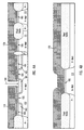
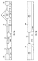
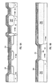
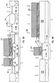
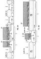
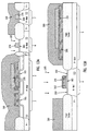
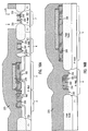
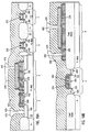
- FIGs. 1A-20A and 1B-20B illustrate the process of this invention.
- Each pair of figures e.g. Figs. 1A and 1B
- FIGs. 1A and 1B represent a cross-sectional view of a set of circuits formed in a single substrate, with the figure designated "A" representing a portion of the substrate to the left of the portion of the substrate shown in the figure designated "B".
- Figs. 1A, 1B, etc show the left hand portion of the substrate
- Figs. 1B, 2B, etc show the right hand portion of the substrate, with the right edge of each "A" figure coinciding with the left edge of the corresponding "B” figure.
- the circuit elements shown in Figs. 1A-20A and 1B-20B are shown at the cross-sections indicated in the plan views of 21A-21E.
- the process begins with a P+ substrate 10 on which a P- epitaxial layer 11 is grown.
- P-wells 110 and 112 and N-wells 111 and 113 are formed in epitaxial layer 11.
- Field oxide regions 100, 101, 102, 103 and 104 and P- field implant regions 100P, 101P, 102P, 103P and 1034P are also formed by means of processes known in the art.
- Field oxide region 101 and P- field implant region 101P isolate P-well 110 from N-well 111, field oxide region 102 and P- field implant region 102P isolate N-well 111 from P-well 112, and field oxide region 103 and P- field implant region 103P isolate P-well 112 from N-well 113.
- NMOS devices of an EEPROM cell will be formed in P-well 110, and conventional (5 volts, 150 ⁇ gate thickness) CMOS devices will be formed in N-well 111 and P-well 112. An additional high-voltage PMOS device will be formed in N-well 113. A capacitor will be formed above field oxide region 104.
- a sacrificial gate oxide layer 120 is formed on the surface of the substrate.
- a threshold voltage adjust implant (represented by arrows 130) for the high-voltage devices to be formed within P-well 110 and N-well 113 is performed through sacrificial gate oxide layer 120. This implant is conducted without a mask and contains the entire dose necessary for setting the threshold voltages of the high-voltage devices within P-well 110 and N-well 113.
- the high-voltage devices will have gate oxides that are relatively thick (for example, 325 ⁇ ).
- Threshold voltage adjust implant 130 also contains part of the implant dose that is required to adjust the threshold voltages of the low-voltage CMOS devices to be formed within N-well 111 and P-well 112.
- a first photoresist mask 140 is then applied to the surface of the substrate.
- An N-type implant 150 is performed through mask 140 to form source/drain regions 160, 161 and 162 within P-well 110.
- Implant 150 consists of two stages (phosphorus and arsenic dopants) so that source/drain regions 160, 161 and 162 are double-diffused, having an N+ region and a deeper surrounding N- region.
- Implant 150 may be performed with arsenic at a dosage of 1 x 10 15 cm -2 and phosphorus at a dosage of 1 x 10 14 cm -2 .
- a gate oxide layer 165 is grown, as shown in Figs. 3A and 3B. Gate oxide layer 165 may be approximately 400 ⁇ thick but is somewhat thicker (for example, 600 ⁇ ) over source/drain regions 160, 161 and 162. As shown in Figs. 4A and 4B, a second, tunnel oxide mask 170 is formed over all of gate oxide layer 165 except a portion thereof above source/drain region 161. A wet etch 180, using a buffered oxide etch (BOE), is then performed to remove the portion of oxide layer 165 which lies under the opening in mask 170. Mask 170 is then removed and, as shown in Figs. 5A and 5B, a tunnel oxide layer 190 is grown over the exposed portion of source/drain region 161. Tunnel oxide 190 is typically about 83 ⁇ thick and adds slightly to the thickness of oxide layer 165 in the other regions.
- BOE buffered oxide etch
- a first polysilicon layer 200 is then deposited over the entire surface of the substrate.
- Polysilicon layer 200 is doped with POCl 3 to approximately 40 ohms per square.
- An oxide-nitride-oxide (ONO) layer 210 is then deposited on polysilicon layer 200.
- the ONO layer may be approximately 260 ⁇ thick.
- a third mask 220 is then deposited over ONO layer 210 and over portions of polysilicon layer 200 that will form a floating gate of a memory transistor 2 and a gate of a select transistor 3, which together will form an EEPROM cell 1 within P-well 110.
- Mask 220 is also deposited over portions of polysilicon layer 200 that will form a gate of a high-voltage PMOS transistor 4 in N-well 113 and the lower electrode of a capacitor 5 above field oxide layer 104.
- polysilicon layer 200 and ONO layer 210 are then etched from all regions except those which underlie mask 220.
- Oxide layer 165 serves as an etch stop for the two-stage plasma etch.
- a boron implant 250 is then conducted to adjust the threshold voltages of the low-voltage CMOS devices to be formed in N-well 111 and P-well 112.
- the dosage of implant 250 may be approximately 3 x 10 12 cm -2 .
- implant 250 supplements the doping which resulted from the prior threshold adjust implant 130 (Figs. 1A and 1B).
- Oxide layer 165 serves as a screen oxide for implant 250.
- gate oxide layer 165 With mask 220 still remaining, the exposed portions of gate oxide layer 165 are then removed.
- a two-step dry/wet etch is the preferred method of removing oxide layer 165 so as to avoid the undercutting of the floating gate of memory transistor 2 (polysilicon layer 200) that may occur if a single wet etch is used.
- Such undercutting forms cavities under the edges of the floating gate and may create problems when a second polysilicon layer is deposited and etched (as described below), since the second polysilicon layer will fill the cavities beneath the floating gate and polysilicon residues or "stringers" may be formed when the second polysilicon layer is later anisotropically etched. These stringers can short out the transistor devices, rendering the circuits inoperable.
- a similar problem occurs in the oxide strata of ONO layer 210. The edges of these strata are etched back by the wet etchant. This can pose a reliability problem.
- a solution to this problem is to use a two-step dry/wet etch.
- an anisotropic etch e.g., using an etchant based on a halocarbon gas such as C 2 F 6
- a wet etch is performed to remove the remaining gate oxide. This etch is performed for the minimum time necessary to remove the oxide layer in order to minimize the undercutting of the floating gate.
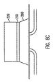
- the etching of polysilicon layer 200 to form the floating gate may be carried out with an etchant that produces a sloped sidewall for the floating gate (see Fig. 8C).
- the etch used to generate the sloped sidewall may be one in which etch inhibitors are generated.
- the etch inhibitors are deposited on the sidewalls, thereby producing the sloped profile of the floating gate.
- An etchant based on a gas chemistry of HCl may be used.
- Oxide layer 260 may be approximately 150 ⁇ thick. Oxide layer 260 grows to a thickness of approximately 300 ⁇ on the exposed sidewalls of polysilicon layer 200.
- a second polysilicon layer 270 is then deposited over the entire surface of the structure.
- a mask 280 shown in Figs. 12A and 12B, is then deposited over portions of polysilicon layer 270 that are to form a control gate of memory transistor 3 and the gates of a low-voltage PMOS transistor 6 to be formed in N-well 111 and a low-voltage NMOS transistor 7 to be formed in P-well 112, respectively.
- Mask 280 is also deposited over a portion of polysilicon layer 270 that is to form the upper electrode of capacitor 5.
- Polysilicon layer 270 is then etched, preferably using a two-stage etching process which includes an anisotropic etch followed by an isotropic etch.
- the isotropic etch is used to remove any stringers from second polysilicon layer 270 that may have formed along the edges of first polysilicon layer 200.
- the control gate (layer 270) of memory transistor 230 is made somewhat smaller than the floating gate (layer 200). This is the case on all sides, as is evident from Fig. 21A, yielding a peripheral region of the floating gate which extends outward beyond the edges the control gate. Since oxide layer 260 is only about 300 ⁇ thick on the vertical edges of the floating gate, "underlapping" the edges of the control gate in this manner prevents shorting in this area. The 300 ⁇ thickness of oxide layer 260 is not by itself sufficient to withstand the biases of 15-17 V commonly found in EEPROM cells.
- capacitor 5 is "underlapped" (see Fig. 21B). This is the preferred structure for capacitor 5 for capacitive matching and leakage considerations.
- Figs. 13A and 13B mask 280 is removed, and a mask 300 is applied over all areas except N-wells 111 and 113.
- a P-type lightly-doped drain ion implant 305 is then performed into the source/drain regions of high-voltage PMOS transistor 4 and low-voltage PMOS transistor 6.
- the lightly-doped drain regions in high-voltage PMOS transistor 4 are designated by the reference numeral 310 in Fig. 14B, and the lightly-doped drain regions for PMOS transistor 6 are designated 320 in Fig. 14A.
- Ion implant 305 may be BF 2 .
- a lightly-doped drain ion implant 340 is conducted into the source/drain regions of low-voltage NMOS transistor 7, forming the lightly-doped drain regions 350 shown in Fig. 15A. Conventional techniques involving deposition and etchback are done to form spacers 360 shown in Figs. 15A and 15B.
- Ion implant 340 may be phosphorus.
- a mask 370 is applied over all areas except P-well 112, and a conventional N+ ion implant 375 is performed to form the heavily-doped regions of the source and drain of low-voltage NMOS transistor 7, both of which are designated by the reference numeral 380 in Fig. 17A.
- the N+ source/drain regions 380 are then annealed.
- a mask 390 is deposited over all areas except N-wells 111 and 113, as shown in Figs. 17A and 17B.
- a conventional P+ ion implant 395 is performed to form the source and drain regions 400 of high-voltage PMOS transistor 4 and the source and drain regions 410 of low-voltage PMOS transistor 6. Source/drain regions 400 and 410 are shown in Figs. 18A and 18B.
- a first dielectric layer 420 is deposited over the entire structure.
- contacts are formed through dielectric layer 420 as follows: a contact 430 is opened to source/drain region 160 of select transistor 3; a contact 440 is opened to the control gate of memory transistor 2 (formed from polysilicon layer 270); three contacts 450 are opened to the bottom electrode of capacitor 5 (formed from polysilicon layer 200); and a contact 460 is opened to the top electrode of capacitor 5 (formed from polysilicon layer 270). Contacts 450 are visible in the plan view of Fig. 21B.
- first metal layer 470 is then deposited and patterned, as shown in Figs. 19A and 19B and Figs. 21A and 21B.
- first metal layer 470 includes a tab 430T which extends from via 430 and a tab 440T which extends from via 440.
- Tab 430 runs to a bit line 470B, which provides an electrical connection to the source/drain region 160 of select transistor 3.
- Bit line 470B extends across the chip and makes connection in a similar manner to the select transistors of other EEPROM cells.
- First metal layer 470 also includes a line 470D which connects through vias 450 to the bottom electrode of capacitor 5, and a line 470E which connects through via 460 to the upper electrode of capacitor 5. Lines 470D and 470E are illustrated in Fig. 21B.
- a second dielectric layer 480 is deposited over the entire structure.
- a via 490 is opened directly above tab 440T, and a second metal layer 500 is deposited and patterned on the surface of second dielectric layer 480.
- the patterning of metal layer 500 forms a word line 500W which extends perpendicular to bit line 470B.
- word line 500W connects to the control gate of memory transistor 2.
- a conventional passivation layer (not shown) is deposited.
- Figs. 21C, 21D and 21E illustrate plan views of high-voltage NMOS transistor 4 and the pair of low-voltage CMOS transistors 6 and 7, respectively.
Landscapes
- Engineering & Computer Science (AREA)
- Manufacturing & Machinery (AREA)
- Non-Volatile Memory (AREA)
- Semiconductor Memories (AREA)
Claims (12)
- Speichertransistor (2) in einer EEPROM-Zelle (1), wobei der Speichertransistor aufweist:ein Paar Source-Drain-Regionen (161, 162), die in einem Substrat (10, 11) ausgebildet sind; ein schwebendes Gate, das über einer der Source-Drain-Regionen (161) und einer Kanalregion, die zwischen den Source-Drain-Regionen liegt, ausgebildet ist, wobei das schwebende Gate von der einen der Source-Drain-Regionen durch ein Tunnel-Gate-Oxid (190) getrennt ist; undein Steuer-Gate (270), welches über dem schwebenden Gate liegt, wobei das Steuergate kleiner als das schwebende Gate ist und so positioniert ist, daß das schwebende Gate sich über den ganzen Umfang des Steuergates seitlich hinaus erstreckt.
- Verfahren zur Herstellung eines Speichertransistors (2) in einer EEPROM-Zelle, wobei das Verfahren aufweist:Bilden eines Halbleitersubstrats (10, 11);Abscheiden einer ersten Maskenschicht (140) auf dem Halbleitersubstrat, um eine Fläche für die Source-Drain-Regionen (161, 162) des Speichertransistors zu definieren, getrennt durch eine Kanalregion, Implantieren von Dotiermitteln, um die Source-Drain-Regionen zu bilden und Entfernen der ersten Maske;Aufwachsen einer Gate-Oxidschicht (165), Abscheiden einer zweiten Maskenschicht (170) auf der Gate-Oxidschicht, um eine Fläche für eine Tunneloxidregion (190) zu definieren, die über einer der Source-Drain-Regionen (161) liegt, Entfernen eines Teils der Gate-Oxidschicht, die durch die zweite Maskenschicht freigelegt ist, um die Tunneloxidregion aufzuwachsen und Entfernen der zweiten Maske;Abscheiden einer ersten leitfähigen Schicht (200) auf der Gate-Oxidschicht und dem Tunneloxid, und Abscheiden einer Isolierschicht (210) auf der ersten leitfähigen Schicht, Abscheiden einer dritten Maskenschicht (220), um eine Fläche für ein schwebendes Gate des Speichertransistors zu definieren, auf dem Tunneloxid, Ausbilden des schwebenden Gates und Entfernen der dritten Maske;Abscheiden einer zweiten leitfähigen Schicht (270) auf der Isolierschicht, Ausbilden einer vierten Maske (280), um Flächen für ein Steuer-Gate des Speichertransistors zu definieren, auf dem schwebenden Gate, Ausbilden des Steuer-Gates und Entfernen der vierten Maske, und wobei das Steuer-Gate kleiner als das schwebende Gate ist, und so positioniert ist, daß das schwebende Gate sich um den gesamten Umfang des Steuer-Gates über dieses seitlich hinaus erstreckt.
- Verfahren zum Herstellen einer EEPROM-Zelle (1), mit einem Speichertransistor, der gemäß Patentanspruch 2 hergestellt ist, und einem Wähltransistor (3), und wobei die erste Maskenschicht auch eine Fläche für eine Source-Drain-Region (160) des Wähltransistors definiert und die dritte Maskenschicht eine Fläche für ein Gate des gewählten Transistors definiert.
- Verfahren nach Anspruch 3, mit wenigstens einem Niederspannungs-MOSFET (6, 7), der hergestellt wird, und wobei die vierte Maskenschicht auch eine Gate-Region für den oder jeden MOSFET definiert.
- Verfahren nach einem der Ansprüche 2 bis 4, wobei nach dem Entfernen der dritten Maske auf die Seitenwände der ersten leitfähigen Schicht eine Oxidschicht (260) aufgewachsen wird.
- Verfahren nach Anspruch 3 oder 4, wobei die dritte Maskenschicht auch eine Fläche für ein Gate eines Hochspannungs-FET (4) definiert.
- Verfahren nach einem der Ansprüche 3, 4 oder 6, wobei die dritte Maskenschicht auch eine Fläche für eine untere Elektrode eines Kondensators (5) definiert und die vierte Maskenschicht eine Fläche für eine obere Elektrode des Kondensators definiert.
- Verfahren nach Anspruch 7, wobei sich die untere Elektrode am gesamten Umfang der oberen Elektrode seitlich über diese hinaus erstreckt.
- Verfahren nach einem der Ansprüche 2 bis 8, wobei das schwebende Gate mit einem Ätzmittel gebildet wird, welches ein schwebendes Gate mit einer geneigten Seitenwand ergibt.
- Verfahren nach einem der Ansprüche 2 bis 9, wobei die erste leitfähige Schicht und die Isolierschicht unter Verwendung der dritten Maske geätzt werden, und zwar zuerst mit einem anisotropen Ätzmittel und dann mit einem isotropen Ätzmittel.
- Verfahren nach einem der Ansprüche 2 bis 8, wobei die Flächen, welche durch die dritte Maske und/oder durch die zweite Maske definiert sind, in einem zweistufigen Trocken/Naß-Ätzvorgang geätzt werden.
- Verfahren nach einem der Ansprüche 2 bis 11, wobei der Schritt Implantieren von Dotiermittel zum Ausbilden der Source-Drain-Region in zwei Stufen durchgeführt wird, wobei die zweite Stufe bei einer niedrigeren Dosierung als die erste Stufe durchgeführt wird, so daß die Source-Drain-Regionen doppelt diffundiert sind.
Applications Claiming Priority (3)
| Application Number | Priority Date | Filing Date | Title |
|---|---|---|---|
| US29823994A | 1994-08-30 | 1994-08-30 | |
| US298239 | 1994-08-30 | ||
| PCT/US1995/011037 WO1996007203A1 (en) | 1994-08-30 | 1995-08-29 | Method of fabrication of an integrated circuit chip containing eeprom and capacitor |
Publications (2)
| Publication Number | Publication Date |
|---|---|
| EP0725980A1 EP0725980A1 (de) | 1996-08-14 |
| EP0725980B1 true EP0725980B1 (de) | 2001-12-05 |
Family
ID=23149650
Family Applications (1)
| Application Number | Title | Priority Date | Filing Date |
|---|---|---|---|
| EP95931647A Expired - Lifetime EP0725980B1 (de) | 1994-08-30 | 1995-08-29 | Herstellungsverfahren für einen ein eeprom und einen kondensator enthaltenden integrierten schaltungschip |
Country Status (5)
| Country | Link |
|---|---|
| US (3) | US5550072A (de) |
| EP (1) | EP0725980B1 (de) |
| KR (1) | KR100355840B1 (de) |
| DE (1) | DE69524376T2 (de) |
| WO (1) | WO1996007203A1 (de) |
Families Citing this family (67)
| Publication number | Priority date | Publication date | Assignee | Title |
|---|---|---|---|---|
| KR0161402B1 (ko) * | 1995-03-22 | 1998-12-01 | 김광호 | 불휘발성 메모리 제조방법 |
| EP0751559B1 (de) * | 1995-06-30 | 2002-11-27 | STMicroelectronics S.r.l. | Herstellungsverfahren eines Schaltkreises, der nichtflüchtige Speicherzellen und Randtransistoren enthält, und entsprechender IC |
| JPH0936257A (ja) * | 1995-07-14 | 1997-02-07 | Matsushita Electron Corp | 半導体記憶装置およびその製造方法 |
| JP3415712B2 (ja) * | 1995-09-19 | 2003-06-09 | 松下電器産業株式会社 | 半導体装置及びその製造方法 |
| KR0168355B1 (ko) * | 1995-11-02 | 1999-02-01 | 김광호 | 반도체장치의 배선 형성방법 |
| EP0788168A1 (de) | 1996-01-31 | 1997-08-06 | STMicroelectronics S.r.l. | Verfahren zur Herstellung nicht-flüchtiger Speicheranordnungen mit schwebendem Gate und so hergestellte Speicheranordnungen |
| US5792708A (en) * | 1996-03-06 | 1998-08-11 | Chartered Semiconductor Manufacturing Pte Ltd. | Method for forming residue free patterned polysilicon layers upon high step height integrated circuit substrates |
| US5605853A (en) * | 1996-05-28 | 1997-02-25 | Taiwan Semiconductor Manufacturing Company Ltd. | Method of making a semiconductor device having 4 transistor SRAM and floating gate memory cells |
| JP3665426B2 (ja) * | 1996-07-17 | 2005-06-29 | 東芝マイクロエレクトロニクス株式会社 | 半導体装置の製造方法 |
| US5960274A (en) * | 1996-08-19 | 1999-09-28 | Advanced Micro Devices, Inc. | Oxide formation process for manufacturing programmable logic device |
| KR100219507B1 (ko) * | 1996-12-17 | 1999-09-01 | 윤종용 | 강유전체 커패시터의 하부전극용 물질층으로 된로컬 인터커넥션을 구비한 반도체장치의 금속배선구조체 및 그 제조방법 |
| JPH10270578A (ja) * | 1997-03-27 | 1998-10-09 | Seiko Instr Inc | 半導体装置及びその製造方法 |
| US5835402A (en) * | 1997-03-27 | 1998-11-10 | Xilinx, Inc. | Non-volatile storage for standard CMOS integrated circuits |
| DE69734278D1 (de) * | 1997-07-03 | 2006-02-09 | St Microelectronics Srl | Herstellungsverfahren eines nichtflüchtigen Halbleiterspeicherbauelementes mit abgeschirmtem Einpolysiliziumgate-Speicherabschnitt |
| JPH1154731A (ja) * | 1997-07-31 | 1999-02-26 | Nec Corp | 半導体装置 |
| US5885871A (en) * | 1997-07-31 | 1999-03-23 | Stmicrolelectronics, Inc. | Method of making EEPROM cell structure |
| US5930613A (en) * | 1997-11-03 | 1999-07-27 | Delco Electronics Corporation | Method of making EPROM in high density CMOS having metallization capacitor |
| US5981335A (en) * | 1997-11-20 | 1999-11-09 | Vanguard International Semiconductor Corporation | Method of making stacked gate memory cell structure |
| US5972749A (en) * | 1998-01-05 | 1999-10-26 | Advanced Micro Devices, Inc. | Method for preventing P1 punchthrough |
| US6040217A (en) * | 1998-04-20 | 2000-03-21 | Lin; Ruei-Ling | Fabricating method of an ultra-fast pseudo-dynamic nonvolatile flash memory |
| US6034395A (en) * | 1998-06-05 | 2000-03-07 | Advanced Micro Devices, Inc. | Semiconductor device having a reduced height floating gate |
| US6380016B2 (en) * | 1998-06-23 | 2002-04-30 | Ross Alan Kohler | Method for forming programmable CMOS ROM devices |
| DE69836423D1 (de) * | 1998-06-30 | 2006-12-28 | St Microelectronics Srl | Verfahren zur Herstellung einer EEPROM-Speicherzelle |
| TW432536B (en) * | 1998-07-16 | 2001-05-01 | United Microelectronics Corp | Method of fabricating an electrically erasable and programmable read-only memory (EEPROM) with improved quality for the tunneling oxide layer therein |
| US6087211A (en) * | 1998-08-12 | 2000-07-11 | National Semiconductor Corporation | Method for forming a semiconductor device having non-volatile memory cells, High-voltage transistors, and low-voltage, deep sub-micron transistors |
| US6069034A (en) * | 1998-09-03 | 2000-05-30 | National Semiconductor Corporation | DMOS architecture using low N-source dose co-driven with P-body implant compatible with E2 PROM core process |
| EP0986100B1 (de) | 1998-09-11 | 2010-05-19 | STMicroelectronics Srl | Elektronisches Bauteil mit EEPROM-Speicherzellen, Hochspannungstransistoren und Niederspannungstransistoren mit Silizidanschlüssen, sowie Herstellungsverfahren desselben |
| KR100277873B1 (ko) * | 1998-12-01 | 2001-01-15 | 김영환 | 반도체 소자의 제조 방법 |
| KR100311971B1 (ko) * | 1998-12-23 | 2001-12-28 | 윤종용 | 비휘발성메모리반도체소자제조방법 |
| US6380581B1 (en) | 1999-02-26 | 2002-04-30 | Micron Technology, Inc. | DRAM technology compatible non volatile memory cells with capacitors connected to the gates of the transistors |
| US6452856B1 (en) | 1999-02-26 | 2002-09-17 | Micron Technology, Inc. | DRAM technology compatible processor/memory chips |
| US6297989B1 (en) | 1999-02-26 | 2001-10-02 | Micron Technology, Inc. | Applications for non-volatile memory cells |
| US6256225B1 (en) * | 1999-02-26 | 2001-07-03 | Micron Technology, Inc. | Construction and application for non-volatile reprogrammable switches |
| US6284637B1 (en) * | 1999-03-29 | 2001-09-04 | Chartered Semiconductor Manufacturing Ltd. | Method to fabricate a floating gate with a sloping sidewall for a flash memory |
| US6472259B1 (en) | 1999-04-01 | 2002-10-29 | Asahi Kasei Microsystems Co., Ltd. | Method of manufacturing semiconductor device |
| US6437839B1 (en) | 1999-04-23 | 2002-08-20 | National Semiconductor Company | Liquid crystal on silicon (LCOS) display pixel with multiple storage capacitors |
| US6177315B1 (en) * | 1999-05-28 | 2001-01-23 | National Semiconductor Corporation | Method of fabricating a high density EEPROM array |
| US6277686B1 (en) * | 1999-07-06 | 2001-08-21 | Taiwan Semiconductor Manufacturing Company | PIP capacitor for split-gate flash process |
| IT1313155B1 (it) * | 1999-08-05 | 2002-06-17 | St Microelectronics Srl | Flusso di processo per la realizzazione di memorie non volatili conrimozione differenziata dell'ossido sacrificale |
| KR20010063021A (ko) * | 1999-12-21 | 2001-07-09 | 윤종용 | 불휘발성 반도체 메모리소자 및 그 제조방법 |
| JP4008651B2 (ja) * | 2000-10-31 | 2007-11-14 | 株式会社東芝 | 半導体装置とその製造方法 |
| US8512525B2 (en) * | 2001-03-12 | 2013-08-20 | Curtiss-Wright Flow Control Corporation | Valve system and method for unheading a coke drum |
| US6403992B1 (en) * | 2001-06-05 | 2002-06-11 | Integrated Technology Express Inc. | Complementary metal-oxide semiconductor device |
| US6983867B1 (en) | 2002-04-29 | 2006-01-10 | Dl Technology Llc | Fluid dispense pump with drip prevention mechanism and method for controlling same |
| US6696350B2 (en) * | 2002-06-13 | 2004-02-24 | Powerchip Semiconductor Corp. | Method of fabricating memory device |
| DE10235072A1 (de) * | 2002-07-31 | 2004-02-26 | Micronas Gmbh | EEPROM-Struktur für Halbleiterspeicher |
| JP4096687B2 (ja) * | 2002-10-09 | 2008-06-04 | 株式会社デンソー | Eepromおよびその製造方法 |
| US7256449B2 (en) * | 2003-05-20 | 2007-08-14 | Samsung Electronics, Co., Ltd. | EEPROM device for increasing a coupling ratio and fabrication method thereof |
| KR100524993B1 (ko) * | 2003-11-28 | 2005-10-31 | 삼성전자주식회사 | 높은 집적도 및 낮은 소스저항을 갖는 이이피롬셀,이이피롬소자 및 그 제조방법 |
| KR20050065143A (ko) * | 2003-12-24 | 2005-06-29 | 매그나칩 반도체 유한회사 | 비휘발성 메모리 소자의 제조 방법 |
| KR100564629B1 (ko) * | 2004-07-06 | 2006-03-28 | 삼성전자주식회사 | 이이피롬 소자 및 그 제조 방법 |
| KR100572327B1 (ko) * | 2004-07-06 | 2006-04-18 | 삼성전자주식회사 | 불휘발성 메모리 소자의 터널링 절연막을 형성하는 방법 |
| KR100618843B1 (ko) * | 2004-07-12 | 2006-09-01 | 삼성전자주식회사 | 비휘발성 반도체 메모리 소자 및 그 제조방법 |
| US7172940B1 (en) * | 2005-09-15 | 2007-02-06 | Ememory Technology Inc. | Method of fabricating an embedded non-volatile memory device |
| US7544558B2 (en) * | 2006-03-13 | 2009-06-09 | Bcd Semiconductor Manufacturing Limited | Method for integrating DMOS into sub-micron CMOS process |
| US7960810B2 (en) | 2006-09-05 | 2011-06-14 | Taiwan Semiconductor Manufacturing Company, Ltd. | Semiconductor device with reliable high-voltage gate oxide and method of manufacture thereof |
| US8707559B1 (en) | 2007-02-20 | 2014-04-29 | Dl Technology, Llc | Material dispense tips and methods for manufacturing the same |
| JP5139712B2 (ja) * | 2007-04-19 | 2013-02-06 | ローム株式会社 | Flotox型eepromおよびその製造方法 |
| US8133783B2 (en) * | 2007-10-26 | 2012-03-13 | Hvvi Semiconductors, Inc. | Semiconductor device having different structures formed simultaneously |
| US8125044B2 (en) * | 2007-10-26 | 2012-02-28 | Hvvi Semiconductors, Inc. | Semiconductor structure having a unidirectional and a bidirectional device and method of manufacture |
| US8108887B2 (en) | 2008-10-30 | 2012-01-31 | The Nielsen Company (Us), Llc | Methods and apparatus for identifying media content using temporal signal characteristics |
| US8864055B2 (en) | 2009-05-01 | 2014-10-21 | Dl Technology, Llc | Material dispense tips and methods for forming the same |
| US8377772B2 (en) * | 2010-08-17 | 2013-02-19 | Texas Instruments Incorporated | CMOS integration method for optimal IO transistor VT |
| JP2018113345A (ja) * | 2017-01-12 | 2018-07-19 | 株式会社東芝 | 半導体装置 |
| US10658364B2 (en) * | 2018-02-28 | 2020-05-19 | Stmicroelectronics S.R.L. | Method for converting a floating gate non-volatile memory cell to a read-only memory cell and circuit structure thereof |
| FR3093591B1 (fr) | 2019-03-06 | 2021-04-02 | St Microelectronics Rousset | Procédé de fabrication d’un élément capacitif haute tension, et circuit intégré correspondant |
| US11746656B1 (en) | 2019-05-13 | 2023-09-05 | DL Technology, LLC. | Micro-volume dispense pump systems and methods |
Family Cites Families (24)
| Publication number | Priority date | Publication date | Assignee | Title |
|---|---|---|---|---|
| US4004159A (en) * | 1973-05-18 | 1977-01-18 | Sanyo Electric Co., Ltd. | Electrically reprogrammable nonvolatile floating gate semi-conductor memory device and method of operation |
| JPS5247684A (en) * | 1975-10-14 | 1977-04-15 | Sanyo Electric Co Ltd | Floating gate type transistor |
| DE3031748A1 (de) * | 1979-08-24 | 1982-03-04 | Centre Electronique Horloger S.A., Neuchâtel | Elektrisch loeschbares und wiederholt programmierbares speicherelement zum dauerhaften speichern |
| JPS56124272A (en) * | 1980-03-05 | 1981-09-29 | Toshiba Corp | Manufacture of semiconductor device |
| US4688078A (en) * | 1982-09-30 | 1987-08-18 | Ning Hseih | Partially relaxable composite dielectric structure |
| JPS62219576A (ja) * | 1986-03-19 | 1987-09-26 | Fujitsu Ltd | Epromの製造方法 |
| IT1191561B (it) * | 1986-06-03 | 1988-03-23 | Sgs Microelettrica Spa | Dispositivo di memoria non labile a semiconduttore con porta non connessa (floating gate) alterabile elettricamente |
| IT1191566B (it) * | 1986-06-27 | 1988-03-23 | Sgs Microelettronica Spa | Dispositivo di memoria non labile a semiconduttore del tipo a porta non connessa (floating gate) alterabile elettricamente con area di tunnel ridotta e procedimento di fabbricazione |
| JPS6329979A (ja) * | 1986-07-23 | 1988-02-08 | Toshiba Corp | 半導体記憶装置 |
| IT1196997B (it) * | 1986-07-25 | 1988-11-25 | Sgs Microelettronica Spa | Processo per realizzare strutture includenti celle di memoria non volatili e2prom con strati di silicio autoallineate transistori associati |
| JPH0777078B2 (ja) * | 1987-01-31 | 1995-08-16 | 株式会社東芝 | 不揮発性半導体メモリ |
| US5243210A (en) * | 1987-02-21 | 1993-09-07 | Kabushiki Kaisha Toshiba | Semiconductor memory device and manufacturing method thereof |
| IT1225873B (it) * | 1987-07-31 | 1990-12-07 | Sgs Microelettrica S P A Catan | Procedimento per la fabbricazione di celle di memoria eprom cmos con riduzione del numero di fasi di mascheratura. |
| JPH01145868A (ja) * | 1987-12-02 | 1989-06-07 | Hitachi Ltd | 浮遊ゲート型不揮発性メモリの製造方法 |
| US4851361A (en) * | 1988-02-04 | 1989-07-25 | Atmel Corporation | Fabrication process for EEPROMS with high voltage transistors |
| US5057448A (en) * | 1988-02-26 | 1991-10-15 | Hitachi, Ltd. | Method of making a semiconductor device having DRAM cells and floating gate memory cells |
| US4859619A (en) * | 1988-07-15 | 1989-08-22 | Atmel Corporation | EPROM fabrication process forming tub regions for high voltage devices |
| IT1237894B (it) * | 1989-12-14 | 1993-06-18 | Sgs Thomson Microelectronics | Processo per la fabbricazione di circuiti integrati comprendenti componenti elettronici di due tipi diversi aventi ciascuno coppie di elettrodi ricavati dagli stessi strati di silicio policristallino e separati da dielettrici diversi |
| US5014098A (en) * | 1990-02-26 | 1991-05-07 | Delco Electronic Corporation | CMOS integrated circuit with EEPROM and method of manufacture |
| US5021848A (en) * | 1990-03-13 | 1991-06-04 | Chiu Te Long | Electrically-erasable and electrically-programmable memory storage devices with self aligned tunnel dielectric area and the method of fabricating thereof |
| DE69232311D1 (de) * | 1992-09-30 | 2002-01-31 | St Microelectronics Srl | Herstellungsverfahren von integrierten Vorrichtungen und so hergestellte integrierte Vorrichtung |
| US5292681A (en) * | 1993-09-16 | 1994-03-08 | Micron Semiconductor, Inc. | Method of processing a semiconductor wafer to form an array of nonvolatile memory devices employing floating gate transistors and peripheral area having CMOS transistors |
| US5543339A (en) * | 1994-08-29 | 1996-08-06 | Motorola, Inc. | Process for forming an electrically programmable read-only memory cell |
| JP3556437B2 (ja) * | 1997-07-25 | 2004-08-18 | 株式会社ルネサステクノロジ | 半導体集積回路装置の製造方法 |
-
1994
- 1994-10-19 US US08/325,855 patent/US5550072A/en not_active Expired - Fee Related
-
1995
- 1995-06-06 US US08/482,319 patent/US5894147A/en not_active Expired - Lifetime
- 1995-06-06 US US08/469,575 patent/US5591658A/en not_active Expired - Lifetime
- 1995-08-29 DE DE69524376T patent/DE69524376T2/de not_active Expired - Lifetime
- 1995-08-29 EP EP95931647A patent/EP0725980B1/de not_active Expired - Lifetime
- 1995-08-29 KR KR1019960701955A patent/KR100355840B1/ko not_active Expired - Lifetime
- 1995-08-29 WO PCT/US1995/011037 patent/WO1996007203A1/en not_active Ceased
Also Published As
| Publication number | Publication date |
|---|---|
| WO1996007203A1 (en) | 1996-03-07 |
| DE69524376T2 (de) | 2002-08-14 |
| KR100355840B1 (ko) | 2003-01-06 |
| US5894147A (en) | 1999-04-13 |
| US5591658A (en) | 1997-01-07 |
| DE69524376D1 (de) | 2002-01-17 |
| EP0725980A1 (de) | 1996-08-14 |
| KR960705356A (ko) | 1996-10-09 |
| US5550072A (en) | 1996-08-27 |
Similar Documents
| Publication | Publication Date | Title |
|---|---|---|
| US5550072A (en) | Method of fabrication of integrated circuit chip containing EEPROM and capacitor | |
| US6346442B1 (en) | Methods for fabricating a semiconductor chip having CMOS devices and a fieldless array | |
| EP1986240B1 (de) | Halbleiterbauelement und Verfahren zur Herstellung eines Halbleiterbauelements | |
| US6174758B1 (en) | Semiconductor chip having fieldless array with salicide gates and methods for making same | |
| CN100565841C (zh) | 半导体装置及其制造方法 | |
| KR100745003B1 (ko) | 반도체 집적 회로 장치 및 그 제조 방법 | |
| US6734065B2 (en) | Method of forming a non-volatile memory device having a metal-oxide-nitride-oxide-semiconductor gate structure | |
| US5466622A (en) | Process for fabricating integrated devices including nonvolatile memories and transistors with tunnel oxide protection | |
| US6770934B1 (en) | Flash memory device structure and manufacturing method thereof | |
| US20020096703A1 (en) | Vertically integrated flash eeprom for greater density and lower cost | |
| EP2648220A1 (de) | Schwebegatespeicher-Bauelement mit Isolationsgraben und dessen Herstellung | |
| JP2003203999A (ja) | 不揮発性半導体記憶装置およびその製造方法 | |
| JPH10116926A (ja) | 凹状のフローティングゲートを具備した不揮発性メモリ素子及びその製造方法 | |
| US5194929A (en) | Nonvolatile semiconductor memory and a memory of manufacturing the same | |
| EP0160003B1 (de) | Mos-speicherzelle mit schwimmendem gate und verfahren zu ihrer verfertigung | |
| US7081381B2 (en) | Flash memory cell and the method of making separate sidewall oxidation | |
| JPH08107157A (ja) | 半導体装置とその製造方法 | |
| US6573142B1 (en) | Method to fabricate self-aligned source and drain in split gate flash | |
| US6700154B1 (en) | EEPROM cell with trench coupling capacitor | |
| US6534364B1 (en) | Tunnel diode layout for an EEPROM cell for protecting the tunnel diode region | |
| US20030170953A1 (en) | Method for forming the self-aligned buried n+ type to diffusion process in etox flash cell | |
| CN121487247B (zh) | 多次可擦除可编程存储器的制备方法 | |
| JPH06112416A (ja) | 集積回路 |
Legal Events
| Date | Code | Title | Description |
|---|---|---|---|
| PUAI | Public reference made under article 153(3) epc to a published international application that has entered the european phase |
Free format text: ORIGINAL CODE: 0009012 |
|
| 17P | Request for examination filed |
Effective date: 19960511 |
|
| AK | Designated contracting states |
Kind code of ref document: A1 Designated state(s): DE FR GB |
|
| 17Q | First examination report despatched |
Effective date: 19980306 |
|
| GRAG | Despatch of communication of intention to grant |
Free format text: ORIGINAL CODE: EPIDOS AGRA |
|
| GRAG | Despatch of communication of intention to grant |
Free format text: ORIGINAL CODE: EPIDOS AGRA |
|
| GRAH | Despatch of communication of intention to grant a patent |
Free format text: ORIGINAL CODE: EPIDOS IGRA |
|
| GRAH | Despatch of communication of intention to grant a patent |
Free format text: ORIGINAL CODE: EPIDOS IGRA |
|
| GRAA | (expected) grant |
Free format text: ORIGINAL CODE: 0009210 |
|
| AK | Designated contracting states |
Kind code of ref document: B1 Designated state(s): DE FR GB |
|
| PG25 | Lapsed in a contracting state [announced via postgrant information from national office to epo] |
Ref country code: FR Free format text: LAPSE BECAUSE OF FAILURE TO SUBMIT A TRANSLATION OF THE DESCRIPTION OR TO PAY THE FEE WITHIN THE PRESCRIBED TIME-LIMIT Effective date: 20011205 |
|
| REG | Reference to a national code |
Ref country code: GB Ref legal event code: IF02 |
|
| REF | Corresponds to: |
Ref document number: 69524376 Country of ref document: DE Date of ref document: 20020117 |
|
| PG25 | Lapsed in a contracting state [announced via postgrant information from national office to epo] |
Ref country code: GB Free format text: LAPSE BECAUSE OF NON-PAYMENT OF DUE FEES Effective date: 20020829 |
|
| PLBE | No opposition filed within time limit |
Free format text: ORIGINAL CODE: 0009261 |
|
| STAA | Information on the status of an ep patent application or granted ep patent |
Free format text: STATUS: NO OPPOSITION FILED WITHIN TIME LIMIT |
|
| EN | Fr: translation not filed | ||
| 26N | No opposition filed | ||
| GBPC | Gb: european patent ceased through non-payment of renewal fee |
Effective date: 20020829 |
|
| PGFP | Annual fee paid to national office [announced via postgrant information from national office to epo] |
Ref country code: DE Payment date: 20120928 Year of fee payment: 18 |
|
| REG | Reference to a national code |
Ref country code: DE Ref legal event code: R082 Ref document number: 69524376 Country of ref document: DE |
|
| PG25 | Lapsed in a contracting state [announced via postgrant information from national office to epo] |
Ref country code: DE Free format text: LAPSE BECAUSE OF NON-PAYMENT OF DUE FEES Effective date: 20140301 |
|
| REG | Reference to a national code |
Ref country code: DE Ref legal event code: R119 Ref document number: 69524376 Country of ref document: DE Effective date: 20140301 |