EP0720230A2 - Structure fusible pour un dispositif de circuit intégré - Google Patents
Structure fusible pour un dispositif de circuit intégré Download PDFInfo
- Publication number
- EP0720230A2 EP0720230A2 EP95120432A EP95120432A EP0720230A2 EP 0720230 A2 EP0720230 A2 EP 0720230A2 EP 95120432 A EP95120432 A EP 95120432A EP 95120432 A EP95120432 A EP 95120432A EP 0720230 A2 EP0720230 A2 EP 0720230A2
- Authority
- EP
- European Patent Office
- Prior art keywords
- integrated circuit
- circuit element
- conductive material
- dielectric material
- fuse
- Prior art date
- Legal status (The legal status is an assumption and is not a legal conclusion. Google has not performed a legal analysis and makes no representation as to the accuracy of the status listed.)
- Granted
Links
- 239000004020 conductor Substances 0.000 claims abstract description 47
- 239000003989 dielectric material Substances 0.000 claims abstract description 35
- 239000000758 substrate Substances 0.000 claims abstract description 18
- 238000004519 manufacturing process Methods 0.000 claims abstract description 15
- 230000001681 protective effect Effects 0.000 claims abstract description 12
- 238000000034 method Methods 0.000 claims description 31
- 239000000463 material Substances 0.000 claims description 11
- 229910021420 polycrystalline silicon Inorganic materials 0.000 claims description 7
- 229920005591 polysilicon Polymers 0.000 claims description 7
- 230000005855 radiation Effects 0.000 claims description 6
- 239000005360 phosphosilicate glass Substances 0.000 claims description 4
- 229910052710 silicon Inorganic materials 0.000 claims description 4
- 239000010703 silicon Substances 0.000 claims description 4
- XUIMIQQOPSSXEZ-UHFFFAOYSA-N Silicon Chemical compound [Si] XUIMIQQOPSSXEZ-UHFFFAOYSA-N 0.000 claims 3
- 238000005304 joining Methods 0.000 claims 3
- 229910021332 silicide Inorganic materials 0.000 claims 3
- FVBUAEGBCNSCDD-UHFFFAOYSA-N silicide(4-) Chemical compound [Si-4] FVBUAEGBCNSCDD-UHFFFAOYSA-N 0.000 claims 3
- 238000000151 deposition Methods 0.000 claims 2
- 239000010410 layer Substances 0.000 abstract description 51
- 239000004065 semiconductor Substances 0.000 abstract description 20
- 239000000155 melt Substances 0.000 abstract description 8
- 239000011241 protective layer Substances 0.000 abstract description 5
- 230000008878 coupling Effects 0.000 abstract description 3
- 238000010168 coupling process Methods 0.000 abstract description 3
- 238000005859 coupling reaction Methods 0.000 abstract description 3
- 230000002950 deficient Effects 0.000 description 6
- 238000013461 design Methods 0.000 description 6
- 238000007664 blowing Methods 0.000 description 4
- 125000006850 spacer group Chemical group 0.000 description 4
- 239000000356 contaminant Substances 0.000 description 3
- 239000012212 insulator Substances 0.000 description 3
- 238000010420 art technique Methods 0.000 description 2
- 230000015556 catabolic process Effects 0.000 description 2
- 238000005260 corrosion Methods 0.000 description 2
- 230000007797 corrosion Effects 0.000 description 2
- 239000013078 crystal Substances 0.000 description 2
- 229910052581 Si3N4 Inorganic materials 0.000 description 1
- VYPSYNLAJGMNEJ-UHFFFAOYSA-N Silicium dioxide Chemical compound O=[Si]=O VYPSYNLAJGMNEJ-UHFFFAOYSA-N 0.000 description 1
- 230000008901 benefit Effects 0.000 description 1
- 239000012141 concentrate Substances 0.000 description 1
- 238000007796 conventional method Methods 0.000 description 1
- 230000000694 effects Effects 0.000 description 1
- 239000012535 impurity Substances 0.000 description 1
- 238000002844 melting Methods 0.000 description 1
- 230000008018 melting Effects 0.000 description 1
- 239000002184 metal Substances 0.000 description 1
- 238000012986 modification Methods 0.000 description 1
- 230000004048 modification Effects 0.000 description 1
- 230000003287 optical effect Effects 0.000 description 1
- 230000008569 process Effects 0.000 description 1
- 238000009877 rendering Methods 0.000 description 1
- HQVNEWCFYHHQES-UHFFFAOYSA-N silicon nitride Chemical compound N12[Si]34N5[Si]62N3[Si]51N64 HQVNEWCFYHHQES-UHFFFAOYSA-N 0.000 description 1
- 229910052814 silicon oxide Inorganic materials 0.000 description 1
- 230000008685 targeting Effects 0.000 description 1
- 238000012360 testing method Methods 0.000 description 1
Images


Classifications
-
- H—ELECTRICITY
- H01—ELECTRIC ELEMENTS
- H01L—SEMICONDUCTOR DEVICES NOT COVERED BY CLASS H10
- H01L27/00—Devices consisting of a plurality of semiconductor or other solid-state components formed in or on a common substrate
- H01L27/02—Devices consisting of a plurality of semiconductor or other solid-state components formed in or on a common substrate including semiconductor components specially adapted for rectifying, oscillating, amplifying or switching and having at least one potential-jump barrier or surface barrier; including integrated passive circuit elements with at least one potential-jump barrier or surface barrier
- H01L27/04—Devices consisting of a plurality of semiconductor or other solid-state components formed in or on a common substrate including semiconductor components specially adapted for rectifying, oscillating, amplifying or switching and having at least one potential-jump barrier or surface barrier; including integrated passive circuit elements with at least one potential-jump barrier or surface barrier the substrate being a semiconductor body
- H01L27/06—Devices consisting of a plurality of semiconductor or other solid-state components formed in or on a common substrate including semiconductor components specially adapted for rectifying, oscillating, amplifying or switching and having at least one potential-jump barrier or surface barrier; including integrated passive circuit elements with at least one potential-jump barrier or surface barrier the substrate being a semiconductor body including a plurality of individual components in a non-repetitive configuration
-
- H—ELECTRICITY
- H01—ELECTRIC ELEMENTS
- H01L—SEMICONDUCTOR DEVICES NOT COVERED BY CLASS H10
- H01L23/00—Details of semiconductor or other solid state devices
- H01L23/52—Arrangements for conducting electric current within the device in operation from one component to another, i.e. interconnections, e.g. wires, lead frames
- H01L23/522—Arrangements for conducting electric current within the device in operation from one component to another, i.e. interconnections, e.g. wires, lead frames including external interconnections consisting of a multilayer structure of conductive and insulating layers inseparably formed on the semiconductor body
- H01L23/525—Arrangements for conducting electric current within the device in operation from one component to another, i.e. interconnections, e.g. wires, lead frames including external interconnections consisting of a multilayer structure of conductive and insulating layers inseparably formed on the semiconductor body with adaptable interconnections
- H01L23/5256—Arrangements for conducting electric current within the device in operation from one component to another, i.e. interconnections, e.g. wires, lead frames including external interconnections consisting of a multilayer structure of conductive and insulating layers inseparably formed on the semiconductor body with adaptable interconnections comprising fuses, i.e. connections having their state changed from conductive to non-conductive
- H01L23/5258—Arrangements for conducting electric current within the device in operation from one component to another, i.e. interconnections, e.g. wires, lead frames including external interconnections consisting of a multilayer structure of conductive and insulating layers inseparably formed on the semiconductor body with adaptable interconnections comprising fuses, i.e. connections having their state changed from conductive to non-conductive the change of state resulting from the use of an external beam, e.g. laser beam or ion beam
-
- H—ELECTRICITY
- H01—ELECTRIC ELEMENTS
- H01L—SEMICONDUCTOR DEVICES NOT COVERED BY CLASS H10
- H01L2924/00—Indexing scheme for arrangements or methods for connecting or disconnecting semiconductor or solid-state bodies as covered by H01L24/00
- H01L2924/0001—Technical content checked by a classifier
- H01L2924/0002—Not covered by any one of groups H01L24/00, H01L24/00 and H01L2224/00
-
- Y—GENERAL TAGGING OF NEW TECHNOLOGICAL DEVELOPMENTS; GENERAL TAGGING OF CROSS-SECTIONAL TECHNOLOGIES SPANNING OVER SEVERAL SECTIONS OF THE IPC; TECHNICAL SUBJECTS COVERED BY FORMER USPC CROSS-REFERENCE ART COLLECTIONS [XRACs] AND DIGESTS
- Y10—TECHNICAL SUBJECTS COVERED BY FORMER USPC
- Y10S—TECHNICAL SUBJECTS COVERED BY FORMER USPC CROSS-REFERENCE ART COLLECTIONS [XRACs] AND DIGESTS
- Y10S148/00—Metal treatment
- Y10S148/055—Fuse
Definitions
- the present invention relates to a fuse element used in conjunction with semiconductor integrated circuits to selectively remove defective circuits from a redundant circuit bank. More specifically, the present invention relates to the structure of a normally open fuse element and the method by which the fuse element is closed.
- Semiconductor integrated circuits contain a large number of electronic devices such as diodes and transistors built onto a single crystal or chip, often made of silicon. Since these devices are so small, their operational integrity is very susceptible to imperfections or impurities in the crystal. The failure of a single transistor in a circuit may render that circuit non-functional.
- the prior art illustrates two common methods for isolating defective circuits. The first is blowing a normally closed fuse. The second is closing a normally open fuse. Both types of fuses are designed for the purpose of enabling a redundant circuit to perform the task of a defective circuit.
- Severing normally closed fuses has certain disadvantages.
- the prior art illustrates many types of fuses that are opened by the application of a large current. The fuse is heated and the material making up the fusible element melts to open the circuit.
- One disadvantage of this type of technique is the fuse material may splatter as it blows, landing on the surface of the device, thereby possibly destroying the device. The current applied to the fuse must be carefully calculated based on the cross-sectional area of the fuse element.
- Another prior art method of opening normally closed fuses is to sever the fuse with a laser beam.
- This method requires that an opening in the outer protective layer be etched over the fuse so that the laser beam can sever the fuse.
- One disadvantage of this method is that the fuse remains exposed to contaminants during fabrication.
- Another disadvantage is that the fuse must be covered with a protective layer after it is severed because there is a risk of corrosion.
- This method also has the similar disadvantage of blowing a fuse with electrical current because debris is created during fusing, thereby possibly rendering the semiconducting device inoperative. Examples of this method are disclosed in U.S. Patent No. 4,795,720, to Kawanabe et al.
- switching to redundant circuits may also be accomplished by selectively closing a normally open fuse to enable functional circuits and isolate the defective circuits.
- the fuse is typically fabricated in horizontal layers with a lower conducting layer and an upper conducting layer separated by a middle insulating layer. A laser beam is used to heat the fuse, thereby breaking down the insulating layer and melting the upper and lower conducting layers together, closing the fuse.
- a disadvantage of this technique is the laser energy applied to the fuse must be carefully calculated to preserve the desired electrical path because the laser beam must pass through one of the conducting layers.
- Another disadvantage of this technique is the fuse is preferably fabricated without a protective layer, possibly exposing the fuse to contaminants. Such a prior art technique is characterized by U.S. Patent No. 4,810,663, to Raffel et al.
- Another type of fuse which is normally open is a link formed where two conducting layers are separated by an insulating layer having an etched hole or a trench.
- This type of fuse is constructed with a lower conducting layer covered by an insulating layer. An opening is etched in the insulating layer. An upper conducting layer is then deposited on the surface of the insulating layer, but in a manner such that the etched opening is not filled with material. A laser beam directed at the opening melts the upper conducting layer which drains into the opening and shorts the upper conducting layer to the lower conducting layer.
- One disadvantage of this method is that it is necessary for the upper conducting to be deposited with some of the material overhanging the edge of the opening in order for there to be enough material to fill the opening and short the conductors.
- An upper conducting layer is deposited over the insulting layer and the filled hole.
- a laser beam directed at the filled hole causes the materials within the hole and the upper and lower conducting layers to react with one another, closing the fuse.
- One disadvantage of this technique is that it requires an elaborate process to fabricate the fuse.
- Another disadvantage is that combination of materials which make up the fuse is limited because the materials must electrically interact with each other under the application of laser energy, otherwise the fuse will not close.
- the prior art demonstrates there is a need for a fusible element that is small enough to be placed anywhere on the semiconducting device without the need for an elaborate manufacturing process or undue restrictions on the design of the fuse. It is, therefor, an object of this invention to create a more reliable, smaller, simpler fuse that does not need to be located in banks. It is a further object of this invention to provide a fusible structure that is less sensitive to etch variations in the oxide layers and more resistant to corrosion.
- the present invention is a normally open fuse element used in conjunction with semiconductor integrated circuits to selectively remove defective circuits from a redundant circuit bank.
- the fuse element is comprised of a central area of conductive material insulated from a plurality of integrated circuit elements by areas of dielectric material.
- the integrated circuit elements and the present invention fuse element are disposed on a semiconductor substrate.
- a thin oxide layer is disposed on the substrate, below the fuse element and the integrated circuit elements to prevent those elements from shorting to the semiconductor substrate or to each other via the semiconductor substrate.
- a protective dielectric layer may be deposited over both the fuse element and the two integrated circuit elements during the manufacture of the overall integrated circuit.
- a laser beam is directed toward the fuse element.
- the laser beam burns through the protective dielectric layer and melts both the conductive material and the dielectric material that form the fuse element. As the fuse element melts, the conductive material contacts the two integrated circuit elements thereby electrically coupling the two integrated circuit elements together.
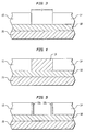
- fuse element 10 is shown disposed between integrated circuit elements 14, 15.
- the integrated circuit elements 14, 15 may be any component leads that may be selectively joined during the manufacture or programming of the overall integrated circuit 11.
- the fuse element 10 is a normally open fuse that electrically isolates the integrated circuit elements 14, 15.
- the fuse element 10 is comprised of a central area of conductive material 12 insulated from the integrated circuit elements 14, 15 by areas of dielectric material 16.
- both the conductive material 12 and the dielectric material 16 are made of materials that readily absorb laser radiation and are easily melted.
- the conductive material 12 is polysilicon and the dielectric material 16 is composed of silicon oxide or silicon nitride.
- the integrated circuit elements 14, 15 and the present invention fuse element 10 are disposed on a semiconductor substrate 20.
- a thin oxide layer 18 is disposed on the substrate, below the fuse element 10 and the integrated circuit elements 14, 15 to prevent those elements from shorting to the semiconductor substrate 20 or to each other via the semiconductor substrate 20.
- At least one protective dielectric layer 22 may be deposited over both the fuse element 10 and the integrated circuit elements 14, 15 during the manufacture of the overall integrated circuit 11.
- the protective dielectric layer 22 is phosphosilicate glass (PSG) which is substantially transparent. As will be explained, a transparent layer helps in targeting a laser on the fuse element 10 and diminishes the amount of optical energy transmitted to the non-fuse elements of the integrated circuit 11.
- PSG phosphosilicate glass
- a laser beam 26 is directed toward the fuse element 10.
- the laser beam 26 burns through the protective dielectric layer 22 and melts both the conductive material 12 and the dielectric material 16 that form the fuse element 10.
- the dielectric material 16 breaks down.
- the molten conductive material 12 contacts the integrated circuit elements 14, 15 thereby electrically coupling the integrated circuit elements 14, 15 together.
- the fuse element 10 is changed from its original normally "open” condition to a "closed” condition.
- the resistance of the "closed" fuse element 10 is less than 1 k ⁇ .
- the two integrated circuit elements 14, 15 are first formed on a thin oxide layer 18 of the semiconductor substrate 20.
- a distance D is left between the integrated circuit elements 14, 15 to later compensate the fuse element 10.
- the distance D between integrated circuit elements 14, 15 is about 0.5 ⁇ m, however other dimensions can be used depending upon the minimum design rules of the manufacturing process.
- a layer of dielectric material 16 is deposited using conventional techniques known in the art between integrated circuit elements 14, 15 as shown in FIG. 4.
- a center region of the deposited dielectric material 16 is etched away using a suitable mask, to form vertical dielectric spacers 16a, 16b.
- the dielectric spacers 16a, 16b are located on the facing sides of the integrated circuit elements 14, 15 as shown in FIG. 5.
- a layer of conductive material 12 is deposited between the dielectric spacers 16a, 16b as shown in FIG. 6.
- the thickness of the layer of conductive material 12 is less than the thickness of the integrated circuit elements 14, 15.
- a center portion of the conductive material 12 is etched away to form a U-shaped structure with a short middle section and two vertical sides of approximately the same thickness as shown in FIG. 7. This shape positions the majority of the conductive material 12 proximate the dielectric spacers 16a, 16b. As such, when laser energy is applied the majority of the molten conductive material is in a position to bypass the melted dielectric material and contact the integrated circuit elements.
- the manufacturing of the fuse element 10 is complete at this point.
- the fuse element 10 may be covered by a transparent protective dielectric layer 22 and one or more cap layers 24 as shown in FIG. 8.
- the cap layers 24 are formed from an oxide.
- the protective dielectric layer 22 and the cap layers 24 covering the fuse element 10 are located at the top of the semiconducting device and prevent external contaminants from contacting the fuse element 10.
- the fuse element 10 described herein can be manufactured as an open structure without any protective layers.
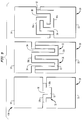
- each fuse element 10 has a different design based on the electrical characteristics of the circuit to be connected and the materials chosen for the conductive material 12 and the integrated circuit elements 14, 15.
- the first fuse element 10 is generally U-shaped and is formed between a section 30 of integrated circuit element 14 which protrudes into a recess 32 formed in integrated circuit element 15. This design has the advantage of being simple and easy to fabricate.
- the second fuse element 10 is generally W-shaped and is formed between two sections 34 of integrated circuit element 14 which protrude into two recesses 36 formed in integrated circuit element 15. This shape maximizes the surface area of each integrated circuit element 14, 15 contacted by the conductive material 12.
- the third fuse element 10 is generally Z-shaped and formed between integrated circuit elements 14, 15 having interlocking L-shaped 38 protrusions. This shape concentrates the surface area of each area of integrated circuit elements 14, 15 in contact with the conductive material 12 into a center region which is then targeted by the laser beam.
Applications Claiming Priority (2)
| Application Number | Priority Date | Filing Date | Title |
|---|---|---|---|
| US36567094A | 1994-12-29 | 1994-12-29 | |
| US365670 | 1994-12-29 |
Publications (3)
| Publication Number | Publication Date |
|---|---|
| EP0720230A2 true EP0720230A2 (fr) | 1996-07-03 |
| EP0720230A3 EP0720230A3 (fr) | 1998-04-15 |
| EP0720230B1 EP0720230B1 (fr) | 2004-09-22 |
Family
ID=23439841
Family Applications (1)
| Application Number | Title | Priority Date | Filing Date |
|---|---|---|---|
| EP95120432A Expired - Lifetime EP0720230B1 (fr) | 1994-12-29 | 1995-12-22 | Structure fusible pour un dispositif de circuit intégré |
Country Status (7)
| Country | Link |
|---|---|
| US (2) | US5827759A (fr) |
| EP (1) | EP0720230B1 (fr) |
| JP (1) | JPH08255553A (fr) |
| KR (1) | KR100405027B1 (fr) |
| AT (1) | ATE277424T1 (fr) |
| DE (1) | DE69533537T2 (fr) |
| TW (1) | TW278229B (fr) |
Families Citing this family (19)
| Publication number | Priority date | Publication date | Assignee | Title |
|---|---|---|---|---|
| US5698895A (en) * | 1994-06-23 | 1997-12-16 | Cubic Memory, Inc. | Silicon segment programming method and apparatus |
| US6218721B1 (en) * | 1997-01-14 | 2001-04-17 | Nec Corporation | Semiconductor device and method of manufacturing the same |
| JPH10229125A (ja) * | 1997-02-14 | 1998-08-25 | Nec Corp | 半導体装置 |
| JPH11154706A (ja) * | 1997-11-20 | 1999-06-08 | Mitsubishi Electric Corp | 半導体装置 |
| US6222244B1 (en) | 1998-06-08 | 2001-04-24 | International Business Machines Corporation | Electrically blowable fuse with reduced cross-sectional area |
| US6524941B2 (en) * | 1998-06-08 | 2003-02-25 | International Business Machines Corporation | Sub-minimum wiring structure |
| US6037648A (en) * | 1998-06-26 | 2000-03-14 | International Business Machines Corporation | Semiconductor structure including a conductive fuse and process for fabrication thereof |
| US6008075A (en) * | 1999-02-11 | 1999-12-28 | Vanguard International Semiconductor Corporation | Method for simultaneous formation of contacts between metal layers and fuse windows in semiconductor manufacturing |
| US20070190751A1 (en) * | 1999-03-29 | 2007-08-16 | Marr Kenneth W | Semiconductor fuses and methods for fabricating and programming the same |
| US6650519B1 (en) | 1999-08-17 | 2003-11-18 | Seagate Technology Llc | ESD protection by a high-to-low resistance shunt |
| US6344679B1 (en) | 1999-11-19 | 2002-02-05 | International Business Machines Corporation | Diode with alterable conductivity and method of making same |
| KR100314133B1 (ko) | 1999-11-26 | 2001-11-15 | 윤종용 | 가장자리에 흡습방지막이 형성된 반도체 칩 및 이흡습방지막의 형성방법 |
| US6489640B1 (en) | 2000-10-06 | 2002-12-03 | National Semiconductor Corporation | Integrated circuit with fuse element and contact pad |
| US6774457B2 (en) * | 2001-09-13 | 2004-08-10 | Texas Instruments Incorporated | Rectangular contact used as a low voltage fuse element |
| US6444503B1 (en) | 2002-02-07 | 2002-09-03 | Taiwan Semiconductor Manufacturing Company | Fabricating electrical metal fuses without additional masking |
| US20040038458A1 (en) * | 2002-08-23 | 2004-02-26 | Marr Kenneth W. | Semiconductor fuses, semiconductor devices containing the same, and methods of making and using the same |
| DE10346460A1 (de) | 2003-10-02 | 2005-05-19 | Infineon Technologies Ag | Anordnung und Verfahren zum Schutz von Fuses/Anti-Fuses |
| US6946718B2 (en) * | 2004-01-05 | 2005-09-20 | Hewlett-Packard Development Company, L.P. | Integrated fuse for multilayered structure |
| US7701035B2 (en) * | 2005-11-30 | 2010-04-20 | International Business Machines Corporation | Laser fuse structures for high power applications |
Citations (3)
| Publication number | Priority date | Publication date | Assignee | Title |
|---|---|---|---|---|
| DE3638799A1 (de) * | 1985-11-14 | 1987-05-21 | Optical Materials Inc | Verfahren zum elektrischen miteinanderverbinden von leitern auf einem substrat sowie dafuer geeignetes substrat |
| US4751197A (en) * | 1984-07-18 | 1988-06-14 | Texas Instruments Incorporated | Make-link programming of semiconductor devices using laser enhanced thermal breakdown of insulator |
| EP0500034A1 (fr) * | 1991-02-19 | 1992-08-26 | Texas Instruments Incorporated | Structure d'antifusible à paroi latérale et procédé de fabrication |
Family Cites Families (25)
| Publication number | Priority date | Publication date | Assignee | Title |
|---|---|---|---|---|
| JPS5847596Y2 (ja) * | 1979-09-05 | 1983-10-29 | 富士通株式会社 | 半導体装置 |
| JPS5694661A (en) * | 1979-12-27 | 1981-07-31 | Fujitsu Ltd | Semiconductor device |
| NL8002634A (nl) * | 1980-05-08 | 1981-12-01 | Philips Nv | Programmeerbare halfgeleiderinrichting en werkwijze ter vervaardiging daarvan. |
| JPS5856355A (ja) * | 1981-09-30 | 1983-04-04 | Hitachi Ltd | 半導体集積回路装置 |
| US4810663A (en) * | 1981-12-07 | 1989-03-07 | Massachusetts Institute Of Technology | Method of forming conductive path by low power laser pulse |
| JPS59104155A (ja) * | 1982-12-07 | 1984-06-15 | Seiko Epson Corp | 半導体ヒユ−ズ |
| US4598462A (en) * | 1983-04-07 | 1986-07-08 | Rca Corporation | Method for making semiconductor device with integral fuse |
| JPS60176250A (ja) * | 1984-02-23 | 1985-09-10 | Toshiba Corp | 半導体装置の製造方法 |
| JPS6122650A (ja) * | 1984-07-11 | 1986-01-31 | Hitachi Ltd | 欠陥救済方法および装置 |
| US4665295A (en) * | 1984-08-02 | 1987-05-12 | Texas Instruments Incorporated | Laser make-link programming of semiconductor devices |
| US4912066A (en) * | 1984-07-18 | 1990-03-27 | Texas Instruments Incorporated | Make-link programming of semiconductor devices using laser-enhanced thermal breakdown of insulator |
| JPS6329953A (ja) * | 1986-07-24 | 1988-02-08 | Matsushita Electronics Corp | 半導体装置 |
| JPS6344739A (ja) * | 1986-08-12 | 1988-02-25 | Fujitsu Ltd | 半導体装置の製造方法 |
| JPS63283060A (ja) * | 1987-05-14 | 1988-11-18 | Fujitsu Ltd | 絶縁分離型半導体装置およびその製造方法 |
| US4875086A (en) * | 1987-05-22 | 1989-10-17 | Texas Instruments Incorporated | Silicon-on-insulator integrated circuits and method |
| DE3728979A1 (de) * | 1987-08-29 | 1989-03-09 | Bosch Gmbh Robert | Planare schaltungsanordnung |
| US5025300A (en) * | 1989-06-30 | 1991-06-18 | At&T Bell Laboratories | Integrated circuits having improved fusible links |
| US5185291A (en) * | 1989-06-30 | 1993-02-09 | At&T Bell Laboratories | Method of making severable conductive path in an integrated-circuit device |
| US5387555A (en) * | 1992-09-03 | 1995-02-07 | Harris Corporation | Bonded wafer processing with metal silicidation |
| DE69127143T2 (de) * | 1990-06-25 | 1997-12-18 | Matsushita Electronics Corp | Kaltkathodenelement |
| US5241496A (en) * | 1991-08-19 | 1993-08-31 | Micron Technology, Inc. | Array of read-only memory cells, eacch of which has a one-time, voltage-programmable antifuse element constructed within a trench shared by a pair of cells |
| US5392187A (en) * | 1992-08-12 | 1995-02-21 | North Carolina State University At Raleigh | Integrated circuit power device with transient responsive current limiting means |
| US5282158A (en) * | 1992-08-21 | 1994-01-25 | Micron Technology, Inc. | Transistor antifuse for a programmable ROM |
| US5395797A (en) * | 1992-12-01 | 1995-03-07 | Texas Instruments Incorporated | Antifuse structure and method of fabrication |
| US5472901A (en) * | 1994-12-02 | 1995-12-05 | Lsi Logic Corporation | Process for formation of vias (or contact openings) and fuses in the same insulation layer with minimal additional steps |
-
1995
- 1995-11-17 TW TW084112222A patent/TW278229B/zh not_active IP Right Cessation
- 1995-12-22 EP EP95120432A patent/EP0720230B1/fr not_active Expired - Lifetime
- 1995-12-22 AT AT95120432T patent/ATE277424T1/de not_active IP Right Cessation
- 1995-12-22 DE DE69533537T patent/DE69533537T2/de not_active Expired - Fee Related
- 1995-12-28 JP JP7343006A patent/JPH08255553A/ja not_active Withdrawn
- 1995-12-29 KR KR1019950066813A patent/KR100405027B1/ko not_active IP Right Cessation
-
1997
- 1997-01-09 US US08/781,571 patent/US5827759A/en not_active Expired - Lifetime
- 1997-03-04 US US08/811,327 patent/US5789794A/en not_active Expired - Lifetime
Patent Citations (3)
| Publication number | Priority date | Publication date | Assignee | Title |
|---|---|---|---|---|
| US4751197A (en) * | 1984-07-18 | 1988-06-14 | Texas Instruments Incorporated | Make-link programming of semiconductor devices using laser enhanced thermal breakdown of insulator |
| DE3638799A1 (de) * | 1985-11-14 | 1987-05-21 | Optical Materials Inc | Verfahren zum elektrischen miteinanderverbinden von leitern auf einem substrat sowie dafuer geeignetes substrat |
| EP0500034A1 (fr) * | 1991-02-19 | 1992-08-26 | Texas Instruments Incorporated | Structure d'antifusible à paroi latérale et procédé de fabrication |
Also Published As
| Publication number | Publication date |
|---|---|
| DE69533537T2 (de) | 2006-07-06 |
| TW278229B (en) | 1996-06-11 |
| US5789794A (en) | 1998-08-04 |
| KR100405027B1 (ko) | 2004-01-07 |
| US5827759A (en) | 1998-10-27 |
| KR960026749A (ko) | 1996-07-22 |
| ATE277424T1 (de) | 2004-10-15 |
| EP0720230A3 (fr) | 1998-04-15 |
| JPH08255553A (ja) | 1996-10-01 |
| DE69533537D1 (de) | 2004-10-28 |
| EP0720230B1 (fr) | 2004-09-22 |
Similar Documents
| Publication | Publication Date | Title |
|---|---|---|
| US5827759A (en) | Method of manufacturing a fuse structure | |
| US6368902B1 (en) | Enhanced efuses by the local degradation of the fuse link | |
| US4628590A (en) | Method of manufacture of a semiconductor device | |
| US6521971B2 (en) | Metal fuse in copper dual damascene | |
| EP1479106B1 (fr) | Amelioration de la programmation de la structure des fusibles par electromigration du siliciure par la creation d'un gradient thermique | |
| US4665295A (en) | Laser make-link programming of semiconductor devices | |
| EP0112675B1 (fr) | Structure de pont activable sélectivement pour former une connexion conductrice dans un circuit intégré | |
| US6649997B2 (en) | Semiconductor device having fuses or anti-fuses | |
| EP0025347B1 (fr) | Dispositifs semiconducteurs comportant des fusibles | |
| CN100541780C (zh) | 可编程半导体器件及其制造和使用方法 | |
| KR100808997B1 (ko) | 퓨즈 소자 및 그 절단 방법 | |
| JPH07335761A (ja) | 電気的にプログラミング可能な自己冷却ヒューズ | |
| JPH0722513A (ja) | 半導体装置及びその製造方法 | |
| EP1831927B1 (fr) | Cellule anti-fusible et son processus de fabrication | |
| JP2000091438A (ja) | 半導体デバイスとその製造方法 | |
| JPH06302775A (ja) | 半導体装置及びその製造方法 | |
| CN100421232C (zh) | 减少非钝化激光熔丝飞溅的半导体器件及其制造方法 | |
| EP0256494A2 (fr) | Liens conducteurs activables pour dispositifs semi-conducteurs | |
| US7029955B2 (en) | Optically and electrically programmable silicided polysilicon fuse device | |
| US5572050A (en) | Fuse-triggered antifuse | |
| KR100501215B1 (ko) | 반도체 디바이스용 퓨즈 | |
| KR950001753B1 (ko) | 반도체장치 및 그 제조방법 | |
| CN1254941A (zh) | 改善熔丝熔断工艺窗口的熔丝布局 | |
| TW567603B (en) | Fuse structure for a semiconductor device and manufacturing method thereof | |
| JPS6193643A (ja) | レ−ザ・ビ−ムでプログラムし得る半導体装置と半導体装置の製法 |
Legal Events
| Date | Code | Title | Description |
|---|---|---|---|
| PUAI | Public reference made under article 153(3) epc to a published international application that has entered the european phase |
Free format text: ORIGINAL CODE: 0009012 |
|
| AK | Designated contracting states |
Kind code of ref document: A2 Designated state(s): AT DE FR GB IE IT NL |
|
| PUAL | Search report despatched |
Free format text: ORIGINAL CODE: 0009013 |
|
| AK | Designated contracting states |
Kind code of ref document: A3 Designated state(s): AT DE FR GB IE IT NL |
|
| 17P | Request for examination filed |
Effective date: 19980805 |
|
| 17Q | First examination report despatched |
Effective date: 20020716 |
|
| GRAP | Despatch of communication of intention to grant a patent |
Free format text: ORIGINAL CODE: EPIDOSNIGR1 |
|
| RAP1 | Party data changed (applicant data changed or rights of an application transferred) |
Owner name: INFINEON TECHNOLOGIES AG |
|
| GRAS | Grant fee paid |
Free format text: ORIGINAL CODE: EPIDOSNIGR3 |
|
| REG | Reference to a national code |
Ref country code: HK Ref legal event code: WD Ref document number: 1003959 Country of ref document: HK |
|
| GRAA | (expected) grant |
Free format text: ORIGINAL CODE: 0009210 |
|
| AK | Designated contracting states |
Kind code of ref document: B1 Designated state(s): AT DE FR GB IE IT NL |
|
| PG25 | Lapsed in a contracting state [announced via postgrant information from national office to epo] |
Ref country code: NL Free format text: LAPSE BECAUSE OF FAILURE TO SUBMIT A TRANSLATION OF THE DESCRIPTION OR TO PAY THE FEE WITHIN THE PRESCRIBED TIME-LIMIT Effective date: 20040922 Ref country code: IT Free format text: LAPSE BECAUSE OF FAILURE TO SUBMIT A TRANSLATION OF THE DESCRIPTION OR TO PAY THE FEE WITHIN THE PRE;WARNING: LAPSES OF ITALIAN PATENTS WITH EFFECTIVE DATE BEFORE 2007 MAY HAVE OCCURRED AT ANY TIME BEFORE 2007. THE CORRECT EFFECTIVE DATE MAY BE DIFFERENT FROM THE ONE RECORDED.SCRIBED TIME-LIMIT Effective date: 20040922 Ref country code: FR Free format text: LAPSE BECAUSE OF FAILURE TO SUBMIT A TRANSLATION OF THE DESCRIPTION OR TO PAY THE FEE WITHIN THE PRESCRIBED TIME-LIMIT Effective date: 20040922 Ref country code: AT Free format text: LAPSE BECAUSE OF FAILURE TO SUBMIT A TRANSLATION OF THE DESCRIPTION OR TO PAY THE FEE WITHIN THE PRESCRIBED TIME-LIMIT Effective date: 20040922 |
|
| REG | Reference to a national code |
Ref country code: GB Ref legal event code: FG4D |
|
| REG | Reference to a national code |
Ref country code: IE Ref legal event code: FG4D |
|
| REF | Corresponds to: |
Ref document number: 69533537 Country of ref document: DE Date of ref document: 20041028 Kind code of ref document: P |
|
| NLV1 | Nl: lapsed or annulled due to failure to fulfill the requirements of art. 29p and 29m of the patents act | ||
| PLBE | No opposition filed within time limit |
Free format text: ORIGINAL CODE: 0009261 |
|
| STAA | Information on the status of an ep patent application or granted ep patent |
Free format text: STATUS: NO OPPOSITION FILED WITHIN TIME LIMIT |
|
| 26N | No opposition filed |
Effective date: 20050623 |
|
| EN | Fr: translation not filed | ||
| PGFP | Annual fee paid to national office [announced via postgrant information from national office to epo] |
Ref country code: GB Payment date: 20061221 Year of fee payment: 12 |
|
| PGFP | Annual fee paid to national office [announced via postgrant information from national office to epo] |
Ref country code: DE Payment date: 20080213 Year of fee payment: 13 |
|
| GBPC | Gb: european patent ceased through non-payment of renewal fee |
Effective date: 20071222 |
|
| PG25 | Lapsed in a contracting state [announced via postgrant information from national office to epo] |
Ref country code: GB Free format text: LAPSE BECAUSE OF NON-PAYMENT OF DUE FEES Effective date: 20071222 |
|
| PGFP | Annual fee paid to national office [announced via postgrant information from national office to epo] |
Ref country code: IE Payment date: 20071220 Year of fee payment: 13 |
|
| REG | Reference to a national code |
Ref country code: IE Ref legal event code: MM4A |
|
| PG25 | Lapsed in a contracting state [announced via postgrant information from national office to epo] |
Ref country code: IE Free format text: LAPSE BECAUSE OF NON-PAYMENT OF DUE FEES Effective date: 20081222 Ref country code: DE Free format text: LAPSE BECAUSE OF NON-PAYMENT OF DUE FEES Effective date: 20090701 |