EP0616334B1 - Nichtfluechtige halbleiterspeicheranordnung mit isolierter gate-elektrode - Google Patents
Nichtfluechtige halbleiterspeicheranordnung mit isolierter gate-elektrode Download PDFInfo
- Publication number
- EP0616334B1 EP0616334B1 EP93922043A EP93922043A EP0616334B1 EP 0616334 B1 EP0616334 B1 EP 0616334B1 EP 93922043 A EP93922043 A EP 93922043A EP 93922043 A EP93922043 A EP 93922043A EP 0616334 B1 EP0616334 B1 EP 0616334B1
- Authority
- EP
- European Patent Office
- Prior art keywords
- erase
- voltage
- well
- signal
- floating gate
- Prior art date
- Legal status (The legal status is an assumption and is not a legal conclusion. Google has not performed a legal analysis and makes no representation as to the accuracy of the status listed.)
- Expired - Lifetime
Links
Images


Classifications
-
- G—PHYSICS
- G11—INFORMATION STORAGE
- G11C—STATIC STORES
- G11C16/00—Erasable programmable read-only memories
- G11C16/02—Erasable programmable read-only memories electrically programmable
- G11C16/06—Auxiliary circuits, e.g. for writing into memory
- G11C16/10—Programming or data input circuits
- G11C16/14—Circuits for erasing electrically, e.g. erase voltage switching circuits
- G11C16/16—Circuits for erasing electrically, e.g. erase voltage switching circuits for erasing blocks, e.g. arrays, words, groups
-
- G—PHYSICS
- G11—INFORMATION STORAGE
- G11C—STATIC STORES
- G11C16/00—Erasable programmable read-only memories
- G11C16/02—Erasable programmable read-only memories electrically programmable
- G11C16/04—Erasable programmable read-only memories electrically programmable using variable threshold transistors, e.g. FAMOS
- G11C16/0408—Erasable programmable read-only memories electrically programmable using variable threshold transistors, e.g. FAMOS comprising cells containing floating gate transistors
- G11C16/0416—Erasable programmable read-only memories electrically programmable using variable threshold transistors, e.g. FAMOS comprising cells containing floating gate transistors comprising cells containing a single floating gate transistor and no select transistor, e.g. UV EPROM
-
- H—ELECTRICITY
- H10—SEMICONDUCTOR DEVICES; ELECTRIC SOLID-STATE DEVICES NOT OTHERWISE PROVIDED FOR
- H10B—ELECTRONIC MEMORY DEVICES
- H10B69/00—Erasable-and-programmable ROM [EPROM] devices not provided for in groups H10B41/00 - H10B63/00, e.g. ultraviolet erasable-and-programmable ROM [UVEPROM] devices
Definitions
- the present invention generally relates to electrically erasable non-volatile semiconductor memory devices (EEPROMs), and more particularly to a so-called flash memory that stores information in the form of electric charges accumulated in a floating gate.
- EEPROMs electrically erasable non-volatile semiconductor memory devices
- Flash memories having a compact and solid construction, are expected to replace bulky and fragile conventional hard disk devices in various computers including laptops.
- each memory cell in the flash memory is formed of a single transistor similar to the memory cell transistor of conventional dynamic random access memories, flash memories can easily realize high integration density and large storage capacity. Further, flash memories lack movable parts such as driving motors and consume little electric power.
- each memory cell has a construction similar to a MOS transistor and includes a source region and a drain region formed in a semiconductor substrate. Further, there is provided a floating gate between the substrate and a control electrode such that the floating gate is insulated by a thin tunneling insulation film, wherein the control electrode corresponds to the gate electrode of conventional MOS transistors.
- a predetermined control voltage is applied to the gate electrode.
- carriers flowing from the source region to the drain region are accelerated in the vicinity of the drain region and are injected to the floating gate through the aforementioned tunneling insulation film.
- the carriers and hence the electric charges thus injected to the floating gate are held therein stably and urge the potential level of the floating gate at a predetermined level.
- the flow of carries from the source to the drain is controlled on and off by the carries stored in the floating gate.
- a potential is applied to the control electrode such that the electric charges in the floating gate are expelled, simultaneously to a potential that is applied to the semiconductor substrate or to the source region in the substrate, for extracting the electric charges from the floating gate.
- the electric charges in the floating gate are dissipated, through the aforementioned tunneling insulation film, either to the semiconductor substrate or to the source region in the substrate.
- FIG.1 schematically shows the construction of the memory cell in the conventional flash memory described above.
- the memory cells are formed on a semiconductor substrate 10, which may be doped to the p-type for example, in rows and columns, wherein each of the memory cells includes an n + -type source region 11a and an n + -type drain region 11b on the substrate 10 such that the regions 11a and 11b are separated from each other by a p-type channel region 10a interposed therebetween.
- the part of the semiconductor substrate 10 corresponding to the channel region 10a is covered by a tunneling insulation film 12a, and a floating gate electrode 12 is provided on the tunneling insulation film 12a.
- the gate electrode 12 is covered by an interlayer insulation film 13a, and a control electrode 13 is provided on the interlayer insulation film 13a.
- a negative source voltage Vs is applied to the source region 11a, and a positive drain voltage Vd is applied to the drain region 11b, such that electrons flow from the source region 11a to the drain region 11b through the channel region 10a.
- a positive control voltage Vg is applied to the control electrode 13.
- the control voltage Vg applied to the control electrode 13 is set to a large negative voltage. Simultaneously, a positive voltage is applied to the substrate 10 as a substrate voltage. Alternatively, a positive voltage is applied to the source region 11a as the source voltage Vs. As a result, the electrons accumulated in the floating gate 12 are expelled to the substrate 10 or to the source region 11a provided in the substrate 10. As a result, the information stored in the memory cell is erased.
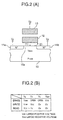
- FIG.2(A) shows the operation of a flash memory cell of the so-called channel erase type wherein the electrons in the floating gate 12 are dissipated to the substrate 10 when erasing information.
- FIG.2(B) shows the setting of the source voltage Vs, the drain voltage Vd, the control voltage Vg and the substrate voltage V SUB for each of the writing, reading and erasing mode for the memory cell of FIG.2(A).
- the tunneling insulation film 12a and the interlayer insulation film 13a are omitted for the sake of simplicity.
- a large negative voltage V MM is applied to the control electrode 13 in the erase mode.
- a positive supply voltage Vcc is applied to the substrate 10.
- the electrons in the floating gate 12 are dissipated to the substrate 10 along a path (1) shown schematically in FIG.2(A).
- the control voltage Vg applied to the control electrode 13 is set to a large positive voltage V PP .
- the electrons are caused to flow from the source region 11a to the drain region 11b, and accelerated electrons are injected to the floating gate 12 in the form of tunneling current, after passing through a path (2) schematically shown in FIG.2(A).
- the supply voltage Vcc is applied to the control electrode 13 via a selected word line, and the drain voltage Vd is set to a positive voltage of about 1 V.
- the electrons flow from the source region 11a to the drain region 11b in the case where there is no electron accumulation in the floating gate 12 and the transistor of FIG.2(A) is turned on.
- FIGS.3(A) and 3(B) show the construction and operation of a flash memory cell that causes a dissipation of the electric charges of the floating gate 12 to the source region 11a, not to the substrate 10, when erasing information.
- the tunneling insulation film 12 and the interlayer insulation film 13a are omitted in FIG.3(A).
- the write mode operation and the read mode operation of the memory cell of FIGS.3(A) and 3(B) are identical with those of the memory cell of FIGS.2(A) and 2(B), only the erase mode operation will be described below.
- the source voltage Vs applied to the source region 11a is set to the positive supply voltage Vcc in the erase mode. Further, the control voltage Vg applied to the control electrode 13 is set to the negative high voltage V MM . On the other hand, the substrate 10 is grounded and the substrate voltage V SUB is set to 0 V. Further, the drain region 11b is set to an opened state. As a result, the electrons in the floating gate 12 are dissipated to the source region 11a along the path (1) shown schematically in FIG.3(A).
- FIG.4 shows an example of the flash memory that uses the memory cell of FIG.2(A).
- the flash memory includes an n-type well 10A formed in the p-type substrate 10, wherein another, p-type well 10B is formed within the n-type well 10A.
- n + -type diffusion regions are formed in correspondence to the source region 11a and the drain region 11b of FIG.2(A), and a number of floating electrodes 12 as well as control electrodes 13 are arranged in rows and columns.
- a double well structure which includes the n-type well 10A and the p-type well 10B, forms a parasitic pnp transistor when constructed on a p-type substrate such as the substrate 10 of FIG.4, it is necessary to apply a voltage V NW to the n-type well 10A when applying the erase voltage V PW to the well 10B, in order to avoid the conduction of the transistor.
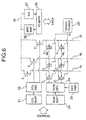
- FIG.5 shows the circuit construction of the flash memory shown in FIG.4.
- memory cells C are disposed in rows and columns on the well 10B, which in turn is formed on the semiconductor substrate 10 shown in FIG.4, wherein those memory cells C aligned in the row direction have respective control electrodes 13 connected commonly with each other by a word line WL.
- those memory cells aligned in the column direction have respective drain regions 11b connected commonly with each other by a bit line BL.
- the word line WL is selected, via an address buffer 23 and a row decoder 24, in response to the row address data supplied to the flash memory device, and the control voltage Vg shown in FIG.2(B) is applied to the selected word line WL.
- the row decoder 24 supplies, in the erase mode, the negative erase voltage V MM shown in FIG.2(B) exclusively to the selected word line WL, based upon the supply voltage supplied from a decoder power supply circuit 25.
- the row decoder 24 further supplies the normal, positive supply voltage Vcc to the unselected word line WL in order to avoid unwanted erase. As a result, only those memory cells C that are connected to the selected word line are erased simultaneously. In other words, the memory cells of the selected memory cell block are erased simultaneously.
- each bit line BL is provided with a corresponding column selection transistor T, wherein the column selection transistor T is selectively turned on and turned off via a column address buffer 21 and a column decoder 22, based upon column address data supplied to the column decoder 22.
- Each bit line BL is connected to a common data line DL via a corresponding column selection transistor T, and an ordinary sense amplifier 27 connected to the line DL discriminates the logic value of the information read out from the selected memory cell C that has been selected in response to the supplied address data.
- the output of the sense amplifier 27 is supplied via an input/output buffer 28 to an output terminal.
- a write amplifier 26 in connection to the line DL for supplying an information signal, which has been supplied via the input/output buffer 28, to a selected bit line BL via the switch transistor T.
- the circuit of FIG.5 includes an erase power supply circuit 29 for applying the erase voltages V NW and V PW to the wells 10A and 10B of FIG.4 in the erase mode, in addition to the foregoing circuits.
- FIG.6 shows a block diagram of a flash memory that uses the memory cell of FIGS.3(A) and 3(B).
- the flash memory of FIG.6 has a construction generally identical to the device of FIG.5, those parts of FIG.6 corresponding to FIG.5 are designated by the same reference numerals and the description thereof will be omitted.
- the source regions of each memory cell transistor C are connected commonly to an erase power supply circuit 29', while the erase power supply circuit 29' produces a source voltage Vs as indicated in FIG.3(B).
- the decoder circuit 25 supplies the erase voltage V MM to the selected word line WL and the positive supply voltage Vcc to the unselected word line WL.
- the flash memories of the type that erases information by causing a dissipation of electric charges to the substrate have the problem of the wells 10A and 10B forming a parasitic bipolar transistor with the substrate 10, as already explained.
- the bias voltage V NW applied to the well 10A and the bias voltage V PW applied to the well 10B have been set equal to the positive supply voltage Vcc.
- the construction to apply the so-called anti-disturb voltage, with the magnitude of about Vcc, to unselected word lines to avoid unwanted erasing of information in unselected memory cell blocks is employed not only in the flash memories of the type to cause the dissipation of electric charges to the substrate in the erase mode but also in the flash memories in which the electric charges are dissipated to the source region.
- such a construction has a problem that there may occur a transient state wherein the anti-disturb voltage is not effectively applied. In such a case, there is a risk that the information that should be retained are unwantedly erased from the memory cell.
- the flash memories of the type shown in FIG.4 that dissipate electric charges in the floating gate 12 to the well 10B in the erase mode tend to show a problem that the p-n junction, formed between the well 10B and the n-type diffusion region 11a that forms the drain region or source region, is subjected to a forward biasing in the erase mode. When this occurs, the bit line BL as well as the source region are charged to the level of the supply voltage Vcc. Further, in the flash memories having the construction to dissipate electric charges in the floating gate to the source region 11a in the erase mode as shown in FIG.3(A), there arises a problem in that the drain region 11b assumes an opened state in the erase mode.
- the anti-disturb voltage is applied to the unselected word lines in this state.
- the electrons are accelerated in the channel region 11a during the dissipation process as they travel from the source region 11a to the drain region 11b (see FIG.3A) and injected to the floating gate 12 in the form of tunneling current.
- a non-volatile semiconductor memory device is known from TOSHIKATSU JINBO ET AL: 'A 5V-ONLY 16 MB FLASH MEMORY WITH SECTOR-ERASE MODE' IEEE INTERNATIONAL SOLID STATE CIRCUITS CONFERENCE, vol. 35, 1 February 1992, pages 154-155, 271, XP 000315799.
- Another object of the present invention is to provide a non-volatile semiconductor memory device having a floating gate for storing information in the floating gate in the form of electric charges, wherein a stable operation is guaranteed even in the transient state.
- the present invention it is ensured to apply a reverse biasing to the p-n junctions formed between the substrate and the first well and between the first well and the second well, by applying the erase voltage first to the first well.
- the flash memory according to the first embodiment of the present invention is constructed on the substrate 10 shown in FIG.4 and has a general circuit construction explained with reference to FIG.5.
- the present invention uses a timing circuit of FIG.7 for adjusting the timing of the erase voltages V NW and V PW produced by the erase power supply circuit 29 respectively for the wells 10A and 10B on the substrate 10.
- the timing circuit is formed of a flip-flop including a NOR gate 113 and a NAND gate 114, wherein the erase voltage signal ERASE produced by the erase power supply circuit 29 is supplied respective first input terminals of the NOR gate 113 and the NAND gate 114. Further, the output signal of the NOR gate 113 is supplied on the one hand to an output terminal via an inverter 115 as an output signal V PW and on the other hand to a second input terminal of the NAND gate 114 via an inverter 112 that has a delay ⁇ .
- the output signal of the NAND gate 114 is supplied on the one hand to an output terminal via an inverter 116 as an output signal V NW and on the other hand to a second input terminal of the NOR gate 113 via another inverter 111 that has a delay ⁇ .
- FIGS.8(A) - 8(C) show the timing of the input signal ERASE supplied to the timing circuit of FIG.7 and the timing of the output signals V NW and V PW .
- the output signal V NW changes from a level H (high) to a level L (low) upon transition of the logic value of the erase voltage signal ERASE supplied from the erase power supply circuit 29 from a level H to a level L. Further, the change of the output signal V NW is transmitted to the NOR gate 113 after a delay ⁇ by the inverter 111, and the output signal V PW of the gate 113 changes from a level H to a level L after a delay ⁇ from the foregoing transition of the input signal ERASE from the level H to the level L. As long as the level of the signal ERASE is L, the foregoing state is maintained.
- the output signal of the NOR gate 113 changes immediately from the level L to the level H. Further, the change of the output level of the NOR gate 113 is transmitted to the NAND gate 114 after a delay ⁇ caused by the inverter 112, and the output signal of the NOR gate 113 changes from the level L to the level H after a delay ⁇ from the transition of the signal ERASE from the level L to the level H.
- the output signal V PW of the NOR gate 113 is applied to the p-type well 10B of FIG.4.
- the output signal V NW of the NAND gate 114 is applied to the n-type well 10A of FIG.4.
- FIG.9 shows the flowchart of the sequence for applying the erase voltage to the substrate 10 of FIG.4 as a result of use of the circuit of FIG.7.
- the erase voltage signal ERASE is produced by the erase power supply circuit 29 in a step S1. Further, in a step S2, the NAND gate 114 produces the erase signal V NW in response to the foregoing erase voltage signal ERASE, and the n-type well 10A in the substrate 10 is biased to the level Vcc for the positive supply voltage. Next, in a step S3, the NOR gate 113 produces the erase signal V PW after a delay ⁇ , and the p-type well 10B in the substrate 10 is biased to the foregoing positive Vcc level.
- step S4 erase of information is conducted in this state in a step S4, wherein the electric charges in the floating gate 12 are dissipated to the substrate 10, more particularly to the p-type well 10B in the substrate 10 after passing through the tunneling insulation film provided under the gate electrode 12.
- step S5 the erase voltage signal ERASE falls, and in response thereto, the erase signal V PW from the NOR gate 113 is canceled in a step S6.
- step S7 the erase signal V NW from the NAND gate 114 is canceled after a delay ⁇ from the moment in which the erase signal V PM is canceled.
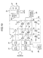
- FIG.10 a second embodiment of the present invention will be described with reference to FIG.10, wherein the circuit of FIG.10 corresponds to the circuit of FIG.5 described with reference to the background art.
- those parts described in FIG.10 are designated by the same reference numerals and the description thereof will be omitted.
- the flash memory of the present embodiment corresponds to the device shown in FIGS.3(A) and 3(B) that dissipates the electric charges from the floating gate to the source region of the memory cell when erasing information.
- the device of FIG.10 uses the erase power supply 29' that is connected commonly to the source regions of the memory cells.
- the flash memory of FIG.10 includes the memory cells arranged in rows and columns on a semiconductor substrate, wherein those memory cells aligned in the row direction have respective control electrodes 13 connected commonly to a word line WL. Similarly, those memory cells aligned in the column direction have respective drain regions connected commonly to a bit line BL.
- the word line WL is selected by the row decoder 24 based upon the address data supplied to the row address buffer 23, while the bit line BL are selected by the column decoder 22 via the switch transistor T, based upon the address data supplied to the column address buffer 21.
- each of the switch transistors T is connected the write amplifier 26 and to the sense amplifier 27 via the common data line DL. Further, the write amplifier 26 and the sense amplifier 27 are connected to the data input/output buffer 28.
- FIG.11(A) shows the construction of the row decoder 24 in the circuit of FIG.10.
- the row decoder 21 includes a NAND gate 121 that is supplied with row address data from the address buffer 23, wherein the NAND gate 121 supplies the output to a latch circuit 124 via an N-channel MOS transistor 122 and a P-channel MOS transistor 124 that are held in the conduction state by the supply voltage Vcc and the substrate voltage V SUB .
- the latch circuit 124 includes a first inverter formed of a P-channel MOS transistor 127 and an N-channel MOS transistor 128 connected in series between a voltage source that supplies a first voltage V 1 and a voltage source that supplies a second voltage V 2 , and a second inverter formed of a P-channel MOS transistor 129 and an N-channel MOS transistor 130 connected in series between the voltage source that supplies the voltage V 1 and the other voltage source that supplies the voltage V 2 , wherein the node in which the transistors 127 and 128 are connected each other, is connected to respective gates of the transistors 129 and 130.
- the output signal of the MOS transistor 123 is supplied to the node where the transistors 127 and 128 are connected commonly, as an input signal of the latch circuit 124.
- the node in which the transistors 129 and 130 are connected each other is connected to respective gates of the transistors 127 and 128.
- the latch circuit 124 produces an output signal at the node where the transistors 129 and 130 are connected each other.
- the output signal of the latch circuit 124 thus obtained is supplied to an output circuit formed of N-channel MOS transistors 125 and 126 connected in series between a voltage source that supplies a voltage V 3 and another voltage source that supplies a voltage V 4 .
- the output signal of the foregoing latch circuit 124 is supplied to the gate of the transistor 125 while the input signal to the latch circuit 124 is supplied to the gate of the transistor 126.
- the output circuit produces the output signal at the node where the transistors 124 and 125 are connected commonly, wherein the output signal thus obtained is supplied to the word line WL.
- FIG.11(B) shows the combination of the voltages V 1 , V 2 , V 3 and V 4 used in the circuit of FIG.11(A) for each of the erasing, writing and reading modes.
- the voltage V 1 is set to the supply voltage level Vcc and the voltage V 2 is set to a negative voltage.
- the output of the latch circuit 124 corresponding to the word line selected by the row address data is held at the level Vcc that corresponds to the voltage V 1 , in correspondence to the fact that the output of the NAND gate 121 is held in the low level state.
- the transistor 125 is turned on and the transistor 126 is turned off.
- a large negative voltage is applied to the word line WL.
- the output voltage of the latch circuits 124 corresponding to the word lines not selected by the row address data are held at a negative voltage V 2 in correspondence to the high level state of the output of the NAND gate 121.
- the transistor 125 of the output circuit does not cause turning-on while the transistor 126 is turned on.
- the unselected word lines WL are applied with an anti-disturb voltage with the magnitude of Vcc.
- the voltage V 1 is set positive while the voltage V 2 is set to the ground level.
- the latch circuit corresponding to the selected word line produces a positive voltage, and the transistor 125 of the output circuit turns on in response thereto.
- the transistor 126 does not turn on because of the low level output of the NAND gate 121.
- the voltage V 3 set to a large positive voltage, is applied to the selected word line WL as a write voltage.
- the latch circuits 124 corresponding to the unselected word lines supply the voltage V 2 set to the ground voltage level, to the transistor 125 as an output signal, in correspondence to the high level state of the output of the NAND gate 121.
- the transistor 125 does not turn on.
- the transistor 126 is turned on by the high level output of the NAND gate 121, and the unselected word line is set to 0 V corresponding to the ground level.
- the voltage V 1 is set to the supply voltage level Vcc. Further, the voltage V 2 is set to 0 V corresponding to the ground level.
- the latch circuit 124 corresponding to the selected word line supplies the output voltage V 1 set to the supply voltage level Vcc to the output transistor 125, and the transistor 125 is turned on in response thereto. Further, the output transistor 126 turns off in response to the low level voltage signal supplied from the NAND gate 121. As a result, a voltage V 3 set to the supply voltage Vcc is supplied to the selected word line as a read control voltage.
- the output voltage of the latch circuits corresponding to the unselected word lines is set to the level V 2 which is equal to the ground level.
- the output transistor 125 is turned off.
- the output transistor 126 is turned on in response to the output of the NAND gate 121, and the voltage V 4 set to zero or ground voltage level is supplied to the word line as the read control voltage.
- the circuit of FIG.10 includes a discharge transistor N in correspondence to each of the bit lines BL for discharging, in the erase mode, the electric charges accumulated on the bit line BL.
- Each of the transistors N is supplied with a common drive signal S DB and turns on in response to the drive signal S DB .
- the corresponding bit line BL is grounded.
- the drive signal S DB of the discharge transistor N is supplied with a timing shown in FIG.12, in order to achieve the activation of the discharge transistor N immediately after the end of the erase mode.
- the signal S DB is produced substantially in correspondence to the trailing edge of the erase signal and is held in the high level state for an interval corresponding to the time constant of the bit line BL.
- FIG.13 shows the timing circuit for producing the signal S DB with the timing shown in FIG.12, wherein the timing circuit includes an inverter 131 supplied with the erase voltage signal ERASE, a time constant circuit RC formed of a resistor 132 and a capacitor 133 for integrating the output of the inverter 131, and a NOR gate 134 supplied with the output of the time constant circuit RC and the erase voltage signal ERASE.
- the NOR gate 134 produces the high level drive signal with the timing shown in FIG.12, for an interval corresponding to the delay time ⁇ of the time constant circuit RC. It is preferred to set the delay time ⁇ approximately equal to the time constant of the bit line BL.
- the row decoder of FIG.11(A) is used also in the flash memory of FIG.4 that causes the electric charges in the floating gate 12 to dissipate into the channel region in the substrate 10.
- the bit line BL experiences a charge up in the erase mode, and it is effective to conduct the discharge of the bit line BL by the discharge circuit 30 of FIG.10.
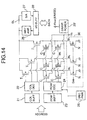
- FIG.14 shows such a construction. As the construction of FIG.14 is obvious from the foregoing explanations, further description will be omitted.
- the flash memory having the circuitry of FIG.10 eliminates the unwanted erasing of information in the unselected memory cells by applying, in the row decoder 24 of FIG.11(A), the anti-disturb voltage to the unselected word lines in the erase mode. More specifically, the level of the voltage V 4 is set, in correspondence to the erase voltage signal, to the supply voltage level Vcc as indicated in FIG.11(B). In order to avoid unwanted erase of information in the transient state immediately after the commencement of the erase mode, it is desired to apply the anti-disturb voltage to the control electrode of the corresponding memory cells before the erase voltage is actually applied to the source region of the memory cells. Further, it is desired to cancel the anti-disturb voltage after the erase voltage is canceled.
- FIG.15 shows the construction of a timing circuit for setting the timing of the anti-disturb voltage with respect to the erase voltage signal ERASE.
- the timing circuit has a construction identical with the construction of the timing circuit shown in FIG.7. Thus, description about the construction of the timing circuit will be omitted.
- the erase voltage signal ERASE is supplied with a timing shown in FIG.8(A), and an anti-disturb signal DIS is formed in response thereto with a timing shown in FIG.8(B).
- an erase voltage signal ERS supplied to the source region of the memory cell is produces with a timing shown in FIG.8(B).
- the voltage V 4 corresponding to the anti-disturb voltage DIS is supplied to the row decoder 24 of FIG.11(A), in advance to the erase voltage signal ERS.
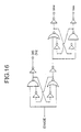
- FIG.16 shows the construction of the timing circuit for implementing the timing adjustment described with reference to FIG.15, to the flash memory having the construction of FIG.4 or FIG.14.
- the illustrated circuit has a construction in which the circuit of FIG.7 is connected to the timing circuit of FIG.15 such that an input terminal of the circuit of FIG.7 supplied with the signal is connected to the output terminal of FIG.15 that supplies the signal ERS.
- the anti-disturb signal DIS and the erase voltage signal V NW to be applied to the well 10A cause a transition first in response to the transition of the erase voltage signal ERASE.
- the signal V PW to be applied to the well 10B causes a transition.
- the erase voltage is applied to the substrate without causing a conduction of the parasitic bipolar transistor in the substrate 10.
- the anti-disturb voltage is applied to the control electrode 13 before the erase voltage is applied to the p-type well in the substrate 10.
- FIG.17 shows a circuit used in the circuit of FIG.11(A) for producing the erase voltage V3 such that the concentration of electric field to the tunneling insulation film 12a is relaxed.
- a large negative voltage corresponding to the voltage V3 is supplied to an input terminal IN, and the negative voltage is supplied to the input terminal of the circuit of FIG.11(A) that receives the voltage V3, via P-channel transistors Tr1 and Tr2.
- the transistors Tr1 and Tr2 conduct when the voltage level on the output terminal is lower than the voltage level of the voltage V3 on the input terminal IN.
- the transistor Tr2 receives, at a gate thereof, positive clock pulses continuously via a capacitor C.
- the negative charges accumulated in the capacitor C as a result of the foregoing negative input voltage are periodically neutralized, and the rate of increase of the voltage on the output terminal OUT is reduced.
- the circuit of FIG.17 is applicable to any of the flash memory of FIG.10 and the flash memory of FIG.14.
- the problem of erroneous writing of information to the memory cell is avoided by discharging the bit lines after the completion of the erase mode operation.
- it becomes possible to extend the lifetime of the flash memory by gradually increasing the voltage applied to the control electrode of the memory cell in the erase mode for avoiding the concentration of electric field to the tunneling insulation film.
Claims (8)
- Nichtflüchtige Halbleiterspeichervorrichtung, aufweisend:dadurch gekennzeichnet, daß das Löschmittel dafür eingerichtet ist, als Antwort auf ein einen Beginn eines Löschens anzeigendes Startsignal ein erstes Löschsignal (VNW) an die erste Mulde und ein zweites Löschsignal (VPW) mit einer zum ersten Löschsignal identischen Polarität an die zweite Mulde so anzulegen, daß das erste Löschsignal vor dem zweiten Löschsignal angelegt wird.ein Halbleitersubstrat (19) mit einem ersten Leitfähigkeitstyp;eine erste Mulde (10A) eines zweiten entgegengesetzten Leitfähigkeitstyps, die auf einer Oberfläche des Halbleitersubstrats so gebildet ist, daß die erste Mulde in dem Halbleitersubstrat enthalten ist;eine zweite Mulde (10B) des ersten Leitfähigkeitstyps, die auf einer Oberfläche der ersten Mulde so gebildet ist, daß die zweite Mulde in der ersten Mulde enthalten ist;eine Mehrzahl von Speicherzellen (C), die in der zweiten Mulde vorgesehen sind, jede der Speicherzellen einen Tunnelisolierungsfilm aufweisend, der auf einer Oberfläche der zweiten Mulde in Entsprechung zu einem Kanalbereich vorgesehen ist und eine Dicke aufweist, um ein Durchtunneln von Trägern zu ermöglichen; eine Elektrode eines schwebenden Gate, die auf dem Tunnelisolierungsfilm vorgesehen ist, um von der Umgebung elektrisch isoliert zu werden, einen Zwischenschicht-Isolierungsfilm, der auf der Elektrode des schwebenden Gate vorgesehen ist; eine Steuerelektrode, die auf dem Zwischenschicht-Isolierungsfilm vorgesehen ist; und ein Paar Diffusionsbereiche des ersten Leitfähigkeitstyps, die auf der zweiten Mulde an beiden Seiten des Kanalbereichs ausgebildet sind; undein Löschmittel (29') zum Dissipieren von in der Elektrode des schwebenden Gate gehaltenen elektrischen Ladungen in den Kanalbereich in der zweiten Mulde durch den Tunnelisolierungsfilm in Form eines Tunnelstroms;
- Nichtflüchtige Halbleiterspeichervorrichtung nach Anspruch 1, worin das Löschmittel (29') dafür eingerichtet ist, das erste Löschsignal (VNW) nach Zurücknehmen des zweiten Löschsignals (VPW) als Antwort auf ein Endsignal zurückzunehmen, das das Ende einer Löschmodus-Operation angibt.
- Nichtflüchtige Halbleiterspeichervorrichtung nach Anspruch 1 oder 2, worin die Mehrzahl Speicherzellen (C) in Reihen und Spalten so angeordnet ist, daß in jeder der Spalten die in der Spalte enthaltenen Speicherzellen jeweilige Drain-Bereiche aufweisen, die gemeinsam durch eine Bitleitung (BL) verbunden sind; und
worin jede der Bitleitungen mit einer Entladeschaltung (30) versehen ist, um auf der Bitleitung akkumulierte elektrische Ladungen zu entladen, welche Entladeschaltung als Antwort auf eine abfallende Flanke eines Löschspannungssignals aktiviert wird, nachdem eine in der Speicherzelle gespeicherte Information gelöscht ist, wodurch die Entladeschaltung eine Entladung der Bitleitungen bewirkt. - Nichtflüchtige Halbleiterspeichervorrichtung nach Anspruch 3, worin die Entladeschaltung einen zwischen der Bitleitung (BL) und einem Erdungspegel vorgesehenen Transistor (N) und eine Steuerschaltung (131 - 134) aufweist, die mit der Löschsteuerspannung versorgt wird, um den Transistor zu veranlassen, als Antwort auf die abfallende Flanke der Löschsteuerspannung einzuschalten, während eines Intervalls (δ) entsprechend einer Zeitkonstante der Bitleitung.
- Nichtflüchtige Halbleiterspeichervorrichtung nach einem der Ansprüche 1 - 4, worin das Löschmittel (29') dafür eingerichtet ist, eine Löschsteuerspannung (ERS) an den Kanalbereich mit einer Polarität und einer Größe so anzulegen, daß in dem schwebenden Gate als Information gehaltene elektrische Ladungen extrahiert werden, das Löschmittel (111 - 116) gleichzeitig eine Antistörungsspannung (DIS) an die Steuerelektrode der Speicherzellen mit Ausnahme der ausgewählten Speicherzelle anlegt, um ein unnötiges Löschen von Information zu vermeiden;
worin das Löschmittel ein Zeitsteuerungs-Einstellmittel (111 - 114) zum Zurücknehmen der Antistörungsspannung (DIS) auf ein Ende eines Löschens von Information hin aufweist, so daß die Antistörungsspannung zurückgenommen wird, nachdem die Löschsteuerspannung (ERS) zurückgenommen ist. - Nichtflüchtige Halbleiterspeichervorrichtung nach Anspruch 5, worin das Zeitsteuerungs-Einstellmittel (111 - 114) dafür eingerichtet ist, bei Beginn eines Löschens von Information die Antistörungsspannung (DIS) anzulegen, so daß die Antistörungsspannung vor der Löschsteuerspannung (ERS) angelegt wird.
- Nichtflüchtige Halbleiterspeichervorrichtung nach einem der Ansprüche 1 - 6, worin das Löschmittel ein internes Verstärkungsmittel (C, Tr1, Tr2) aufweist, um eine Steuerspannung an die Steuerelektrode der ausgewählten Speicherzelle zu liefern, um in der Elektrode des schwebenden Gate akkumulierte elektrische Ladungen auszutreiben, welches interne Verstärkungsmittel eine allmähliche Erhöhung der Steuerspannung bewirkt.
- Nichtflüchtige Halbleiterspeichervorrichtung nach Anspruch 7, worin das interne Verstärkungsmittel ein Stromzufuhrmittel (Tr1, Tr2) aufweist, das mit der Steuerspannung von der Spannungsquelle versorgt wird, um elektrische Ladungen an die Elektrode des schwebenden Gate als Antwort darauf zu liefern, und ein Leckmittel (C), das mit einem periodischen Pulssignal versorgt wird, um elektrische Ladungen periodisch vom Stromzufuhrmittel als Antwort auf das Pulssignal zu entfernen.
Applications Claiming Priority (4)
| Application Number | Priority Date | Filing Date | Title |
|---|---|---|---|
| JP26741292A JP3152762B2 (ja) | 1992-10-06 | 1992-10-06 | 不揮発性半導体記憶装置 |
| JP26741292 | 1992-10-06 | ||
| JP267412/92 | 1992-10-06 | ||
| PCT/JP1993/001438 WO1994008340A1 (en) | 1992-10-06 | 1993-10-06 | Non-volatile semiconductor memory device having floating gate |
Publications (3)
| Publication Number | Publication Date |
|---|---|
| EP0616334A1 EP0616334A1 (de) | 1994-09-21 |
| EP0616334A4 EP0616334A4 (de) | 1999-03-24 |
| EP0616334B1 true EP0616334B1 (de) | 2002-01-30 |
Family
ID=17444493
Family Applications (1)
| Application Number | Title | Priority Date | Filing Date |
|---|---|---|---|
| EP93922043A Expired - Lifetime EP0616334B1 (de) | 1992-10-06 | 1993-10-06 | Nichtfluechtige halbleiterspeicheranordnung mit isolierter gate-elektrode |
Country Status (6)
| Country | Link |
|---|---|
| US (1) | US5521866A (de) |
| EP (1) | EP0616334B1 (de) |
| JP (1) | JP3152762B2 (de) |
| KR (1) | KR970004072B1 (de) |
| DE (1) | DE69331519T2 (de) |
| WO (1) | WO1994008340A1 (de) |
Families Citing this family (26)
| Publication number | Priority date | Publication date | Assignee | Title |
|---|---|---|---|---|
| US5541875A (en) * | 1994-07-01 | 1996-07-30 | Advanced Micro Devices, Inc. | High energy buried layer implant to provide a low resistance p-well in a flash EPROM array |
| KR19980064091A (ko) * | 1996-12-13 | 1998-10-07 | 윌리엄비.켐플러 | 신뢰성과 동작성이 개선된 채널 핫 전자 프로그램 방식 메모리디바이스 |
| US5862078A (en) * | 1997-08-11 | 1999-01-19 | Taiwan Semiconductor Manufacturing Company, Ltd. | Mixed mode erase method to improve flash eeprom write/erase threshold closure |
| US5838618A (en) * | 1997-09-11 | 1998-11-17 | Taiwan Semiconductor Manufacturing Company Ltd. | Bi-modal erase method for eliminating cycling-induced flash EEPROM cell write/erase threshold closure |
| US5949717A (en) * | 1997-09-12 | 1999-09-07 | Taiwan Semiconductor Manufacturing Company, Ltd. | Method to improve flash EEPROM cell write/erase threshold voltage closure |
| US5903499A (en) * | 1997-09-12 | 1999-05-11 | Taiwan Semiconductor Manufacturing Company, Ltd. | Method to erase a flash EEPROM using negative gate source erase followed by a high negative gate erase |
| JP3175665B2 (ja) * | 1997-10-24 | 2001-06-11 | 日本電気株式会社 | 不揮発性半導体記憶装置のデータ消去方法 |
| US6359810B1 (en) * | 1998-03-13 | 2002-03-19 | Atmel Corporation | Page mode erase in a flash memory array |
| US6005809A (en) * | 1998-06-19 | 1999-12-21 | Taiwan Semiconductor Manufacturing Company, Ltd. | Program and erase method for a split gate flash EEPROM |
| US6049484A (en) * | 1998-09-10 | 2000-04-11 | Taiwan Semiconductor Manufacturing Company | Erase method to improve flash EEPROM endurance by combining high voltage source erase and negative gate erase |
| US6049486A (en) * | 1999-01-04 | 2000-04-11 | Taiwan Semiconductor Manufacturing Company | Triple mode erase scheme for improving flash EEPROM cell threshold voltage (VT) cycling closure effect |
| JP2001102553A (ja) * | 1999-09-29 | 2001-04-13 | Sony Corp | 半導体装置、その駆動方法および製造方法 |
| JP3633853B2 (ja) * | 2000-06-09 | 2005-03-30 | Necエレクトロニクス株式会社 | フラッシュメモリの消去動作制御方法およびフラッシュメモリの消去動作制御装置 |
| KR100418718B1 (ko) * | 2000-06-29 | 2004-02-14 | 주식회사 하이닉스반도체 | 플래쉬 메모리 셀의 소거 방법 |
| US6510084B2 (en) * | 2001-05-21 | 2003-01-21 | Winbond Electronics Corporation | Column decoder with increased immunity to high voltage breakdown |
| US6614693B1 (en) | 2002-03-19 | 2003-09-02 | Taiwan Semiconductor Manufacturing Company | Combination erase waveform to reduce oxide trapping centers generation rate of flash EEPROM |
| US6876582B2 (en) * | 2002-05-24 | 2005-04-05 | Hynix Semiconductor, Inc. | Flash memory cell erase scheme using both source and channel regions |
| US6830650B2 (en) * | 2002-07-12 | 2004-12-14 | Advanced Energy Industries, Inc. | Wafer probe for measuring plasma and surface characteristics in plasma processing environments |
| US6859392B2 (en) * | 2002-08-26 | 2005-02-22 | Micron Technology, Inc. | Preconditioning global bitlines |
| US7397699B2 (en) * | 2005-07-27 | 2008-07-08 | Atmel Corporation | Channel discharging after erasing flash memory devices |
| US7692960B2 (en) * | 2006-12-20 | 2010-04-06 | Macronix International Co., Ltd. | Scheme of semiconductor memory and method for operating same |
| KR20110099564A (ko) | 2010-03-02 | 2011-09-08 | 삼성전자주식회사 | 리페어 효율을 향상하기 위한 플래시 메모리 장치 및 그것의 동작 방법 |
| US8644079B2 (en) * | 2011-05-10 | 2014-02-04 | Marco Passerini | Method and circuit to discharge bit lines after an erase pulse |
| US10381085B2 (en) * | 2016-10-27 | 2019-08-13 | Micron Technogy, Inc. | Erasing memory cells |
| GB201711298D0 (en) | 2017-07-13 | 2017-08-30 | Univ Birmingham | Elimination of commutation failure of LCC HVDC system |
| US10984871B2 (en) * | 2017-11-22 | 2021-04-20 | Samsung Electronics Co., Ltd. | Non-volatile memory device and method of erasing the same |
Family Cites Families (10)
| Publication number | Priority date | Publication date | Assignee | Title |
|---|---|---|---|---|
| JP2504743B2 (ja) * | 1985-03-18 | 1996-06-05 | 日本電気株式会社 | 半導体記憶装置 |
| FR2616953B1 (fr) * | 1987-06-16 | 1989-08-25 | Thomson Semiconducteurs | Memoire eprom effacable par impulsions |
| JPH0715799B2 (ja) * | 1987-06-30 | 1995-02-22 | 日本電気株式会社 | 半導体記憶装置 |
| JP2685770B2 (ja) * | 1987-12-28 | 1997-12-03 | 株式会社東芝 | 不揮発性半導体記憶装置 |
| JPH0793021B2 (ja) * | 1988-12-20 | 1995-10-09 | 三菱電機株式会社 | 不揮発性半導体記憶装置 |
| JP3099887B2 (ja) * | 1990-04-12 | 2000-10-16 | 株式会社東芝 | 不揮発性半導体記憶装置 |
| JPH0478097A (ja) * | 1990-07-13 | 1992-03-12 | Sony Corp | メモリ装置 |
| KR920006988A (ko) * | 1990-09-25 | 1992-04-28 | 아오이 죠이치 | 불휘발성 반도체메모리 |
| US5265059A (en) * | 1991-05-10 | 1993-11-23 | Intel Corporation | Circuitry and method for discharging a drain of a cell of a non-volatile semiconductor memory |
| JPH05102438A (ja) * | 1991-10-04 | 1993-04-23 | Mitsubishi Electric Corp | 不揮発性半導体記憶装置 |
-
1992
- 1992-10-06 JP JP26741292A patent/JP3152762B2/ja not_active Expired - Lifetime
-
1993
- 1993-10-06 KR KR1019940701876A patent/KR970004072B1/ko active
- 1993-10-06 EP EP93922043A patent/EP0616334B1/de not_active Expired - Lifetime
- 1993-10-06 WO PCT/JP1993/001438 patent/WO1994008340A1/ja active IP Right Grant
- 1993-10-06 DE DE69331519T patent/DE69331519T2/de not_active Expired - Lifetime
- 1993-10-06 US US08/244,634 patent/US5521866A/en not_active Expired - Lifetime
Also Published As
| Publication number | Publication date |
|---|---|
| EP0616334A1 (de) | 1994-09-21 |
| KR970004072B1 (ko) | 1997-03-24 |
| EP0616334A4 (de) | 1999-03-24 |
| WO1994008340A1 (en) | 1994-04-14 |
| DE69331519T2 (de) | 2002-06-20 |
| US5521866A (en) | 1996-05-28 |
| DE69331519D1 (de) | 2002-03-14 |
| JPH06119790A (ja) | 1994-04-28 |
| JP3152762B2 (ja) | 2001-04-03 |
Similar Documents
| Publication | Publication Date | Title |
|---|---|---|
| EP0616334B1 (de) | Nichtfluechtige halbleiterspeicheranordnung mit isolierter gate-elektrode | |
| JP3091687B2 (ja) | センス増幅回路 | |
| US4377857A (en) | Electrically erasable programmable read-only memory | |
| US8687455B2 (en) | Nonvolatile semiconductor memory | |
| KR930000818B1 (ko) | Nand 메모리셀 구조를 갖춘 eeprom | |
| JP2002197881A (ja) | レベルシフタ及びレベルシフタを備えた半導体記憶装置 | |
| JP3451118B2 (ja) | 半導体不揮発性記憶装置 | |
| US5748531A (en) | Common source line control circuit for preventing snap back breakdown | |
| JPH11120779A (ja) | 不揮発性半導体記憶装置 | |
| US6421272B1 (en) | Non-volatile semiconductor memory device | |
| US3858060A (en) | Integrated driver circuit | |
| JPH0154796B2 (de) | ||
| JP3935592B2 (ja) | 内部電位発生回路 | |
| JPS6322626B2 (de) | ||
| US5943268A (en) | Non-volatile latch having PMOS floating gate memory cells | |
| JP2510521B2 (ja) | Eeprom装置 | |
| US6507521B2 (en) | Semiconductor memory system | |
| US20030128575A1 (en) | Three-transistor sram device | |
| JPH06103790A (ja) | 不揮発性半導体記憶装置 | |
| JP3011570B2 (ja) | 半導体メモリ | |
| JP3160451B2 (ja) | 不揮発性半導体記憶装置 | |
| JPH0527195B2 (de) | ||
| JP2648099B2 (ja) | 不揮発性半導体メモリ装置およびそのデータ消去方法 | |
| JP2625298B2 (ja) | 不揮発性半導体記憶装置 | |
| JPH0770233B2 (ja) | 不揮発性半導体記憶装置の書込および消去方法 |
Legal Events
| Date | Code | Title | Description |
|---|---|---|---|
| PUAI | Public reference made under article 153(3) epc to a published international application that has entered the european phase |
Free format text: ORIGINAL CODE: 0009012 |
|
| 17P | Request for examination filed |
Effective date: 19940605 |
|
| AK | Designated contracting states |
Kind code of ref document: A1 Designated state(s): DE FR GB |
|
| A4 | Supplementary search report drawn up and despatched |
Effective date: 19990209 |
|
| AK | Designated contracting states |
Kind code of ref document: A4 Designated state(s): DE FR GB |
|
| 17Q | First examination report despatched |
Effective date: 19990823 |
|
| GRAG | Despatch of communication of intention to grant |
Free format text: ORIGINAL CODE: EPIDOS AGRA |
|
| GRAG | Despatch of communication of intention to grant |
Free format text: ORIGINAL CODE: EPIDOS AGRA |
|
| GRAG | Despatch of communication of intention to grant |
Free format text: ORIGINAL CODE: EPIDOS AGRA |
|
| GRAH | Despatch of communication of intention to grant a patent |
Free format text: ORIGINAL CODE: EPIDOS IGRA |
|
| GRAH | Despatch of communication of intention to grant a patent |
Free format text: ORIGINAL CODE: EPIDOS IGRA |
|
| GRAA | (expected) grant |
Free format text: ORIGINAL CODE: 0009210 |
|
| REG | Reference to a national code |
Ref country code: GB Ref legal event code: IF02 |
|
| AK | Designated contracting states |
Kind code of ref document: B1 Designated state(s): DE FR GB |
|
| REF | Corresponds to: |
Ref document number: 69331519 Country of ref document: DE Date of ref document: 20020314 |
|
| ET | Fr: translation filed | ||
| PLBE | No opposition filed within time limit |
Free format text: ORIGINAL CODE: 0009261 |
|
| STAA | Information on the status of an ep patent application or granted ep patent |
Free format text: STATUS: NO OPPOSITION FILED WITHIN TIME LIMIT |
|
| 26N | No opposition filed | ||
| REG | Reference to a national code |
Ref country code: GB Ref legal event code: 732E |
|
| REG | Reference to a national code |
Ref country code: FR Ref legal event code: TP |
|
| PGFP | Annual fee paid to national office [announced via postgrant information from national office to epo] |
Ref country code: GB Payment date: 20090930 Year of fee payment: 17 |
|
| PGFP | Annual fee paid to national office [announced via postgrant information from national office to epo] |
Ref country code: FR Payment date: 20091029 Year of fee payment: 17 |
|
| GBPC | Gb: european patent ceased through non-payment of renewal fee |
Effective date: 20101006 |
|
| PG25 | Lapsed in a contracting state [announced via postgrant information from national office to epo] |
Ref country code: FR Free format text: LAPSE BECAUSE OF NON-PAYMENT OF DUE FEES Effective date: 20101102 |
|
| REG | Reference to a national code |
Ref country code: FR Ref legal event code: ST Effective date: 20110630 |
|
| PG25 | Lapsed in a contracting state [announced via postgrant information from national office to epo] |
Ref country code: GB Free format text: LAPSE BECAUSE OF NON-PAYMENT OF DUE FEES Effective date: 20101006 |
|
| PGFP | Annual fee paid to national office [announced via postgrant information from national office to epo] |
Ref country code: DE Payment date: 20121003 Year of fee payment: 20 |
|
| REG | Reference to a national code |
Ref country code: DE Ref legal event code: R071 Ref document number: 69331519 Country of ref document: DE |
|
| PG25 | Lapsed in a contracting state [announced via postgrant information from national office to epo] |
Ref country code: DE Free format text: LAPSE BECAUSE OF EXPIRATION OF PROTECTION Effective date: 20131008 |