EP0592690B1 - Verfahren zur identifizierung einer optischen linie - Google Patents
Verfahren zur identifizierung einer optischen linie Download PDFInfo
- Publication number
- EP0592690B1 EP0592690B1 EP93911952A EP93911952A EP0592690B1 EP 0592690 B1 EP0592690 B1 EP 0592690B1 EP 93911952 A EP93911952 A EP 93911952A EP 93911952 A EP93911952 A EP 93911952A EP 0592690 B1 EP0592690 B1 EP 0592690B1
- Authority
- EP
- European Patent Office
- Prior art keywords
- optical line
- light
- optical
- reflecting
- detecting
- Prior art date
- Legal status (The legal status is an assumption and is not a legal conclusion. Google has not performed a legal analysis and makes no representation as to the accuracy of the status listed.)
- Expired - Lifetime
Links
Images


Classifications
-
- G—PHYSICS
- G02—OPTICS
- G02B—OPTICAL ELEMENTS, SYSTEMS OR APPARATUS
- G02B6/00—Light guides; Structural details of arrangements comprising light guides and other optical elements, e.g. couplings
- G02B6/24—Coupling light guides
- G02B6/26—Optical coupling means
- G02B6/28—Optical coupling means having data bus means, i.e. plural waveguides interconnected and providing an inherently bidirectional system by mixing and splitting signals
- G02B6/293—Optical coupling means having data bus means, i.e. plural waveguides interconnected and providing an inherently bidirectional system by mixing and splitting signals with wavelength selective means
- G02B6/29304—Optical coupling means having data bus means, i.e. plural waveguides interconnected and providing an inherently bidirectional system by mixing and splitting signals with wavelength selective means operating by diffraction, e.g. grating
- G02B6/29305—Optical coupling means having data bus means, i.e. plural waveguides interconnected and providing an inherently bidirectional system by mixing and splitting signals with wavelength selective means operating by diffraction, e.g. grating as bulk element, i.e. free space arrangement external to a light guide
- G02B6/29311—Diffractive element operating in transmission
-
- G—PHYSICS
- G01—MEASURING; TESTING
- G01M—TESTING STATIC OR DYNAMIC BALANCE OF MACHINES OR STRUCTURES; TESTING OF STRUCTURES OR APPARATUS, NOT OTHERWISE PROVIDED FOR
- G01M11/00—Testing of optical apparatus; Testing structures by optical methods not otherwise provided for
-
- G—PHYSICS
- G01—MEASURING; TESTING
- G01M—TESTING STATIC OR DYNAMIC BALANCE OF MACHINES OR STRUCTURES; TESTING OF STRUCTURES OR APPARATUS, NOT OTHERWISE PROVIDED FOR
- G01M11/00—Testing of optical apparatus; Testing structures by optical methods not otherwise provided for
- G01M11/30—Testing of optical devices, constituted by fibre optics or optical waveguides
- G01M11/31—Testing of optical devices, constituted by fibre optics or optical waveguides with a light emitter and a light receiver being disposed at the same side of a fibre or waveguide end-face, e.g. reflectometers
- G01M11/3109—Reflectometers detecting the back-scattered light in the time-domain, e.g. OTDR
- G01M11/3118—Reflectometers detecting the back-scattered light in the time-domain, e.g. OTDR using coded light-pulse sequences
-
- G—PHYSICS
- G02—OPTICS
- G02B—OPTICAL ELEMENTS, SYSTEMS OR APPARATUS
- G02B6/00—Light guides; Structural details of arrangements comprising light guides and other optical elements, e.g. couplings
-
- G—PHYSICS
- G02—OPTICS
- G02B—OPTICAL ELEMENTS, SYSTEMS OR APPARATUS
- G02B6/00—Light guides; Structural details of arrangements comprising light guides and other optical elements, e.g. couplings
- G02B6/02—Optical fibres with cladding with or without a coating
- G02B6/02057—Optical fibres with cladding with or without a coating comprising gratings
- G02B6/02076—Refractive index modulation gratings, e.g. Bragg gratings
-
- G—PHYSICS
- G02—OPTICS
- G02B—OPTICAL ELEMENTS, SYSTEMS OR APPARATUS
- G02B6/00—Light guides; Structural details of arrangements comprising light guides and other optical elements, e.g. couplings
- G02B6/24—Coupling light guides
- G02B6/42—Coupling light guides with opto-electronic elements
- G02B6/4201—Packages, e.g. shape, construction, internal or external details
- G02B6/4246—Bidirectionally operating package structures
-
- G—PHYSICS
- G02—OPTICS
- G02B—OPTICAL ELEMENTS, SYSTEMS OR APPARATUS
- G02B6/00—Light guides; Structural details of arrangements comprising light guides and other optical elements, e.g. couplings
- G02B6/44—Mechanical structures for providing tensile strength and external protection for fibres, e.g. optical transmission cables
- G02B6/4479—Manufacturing methods of optical cables
- G02B6/4482—Code or colour marking
-
- G—PHYSICS
- G02—OPTICS
- G02B—OPTICAL ELEMENTS, SYSTEMS OR APPARATUS
- G02B6/00—Light guides; Structural details of arrangements comprising light guides and other optical elements, e.g. couplings
- G02B6/46—Processes or apparatus adapted for installing or repairing optical fibres or optical cables
- G02B6/56—Processes for repairing optical cables
- G02B6/562—Processes for repairing optical cables locatable, e.g. using magnetic means
-
- H—ELECTRICITY
- H04—ELECTRIC COMMUNICATION TECHNIQUE
- H04B—TRANSMISSION
- H04B10/00—Transmission systems employing electromagnetic waves other than radio-waves, e.g. infrared, visible or ultraviolet light, or employing corpuscular radiation, e.g. quantum communication
- H04B10/07—Arrangements for monitoring or testing transmission systems; Arrangements for fault measurement of transmission systems
- H04B10/071—Arrangements for monitoring or testing transmission systems; Arrangements for fault measurement of transmission systems using a reflected signal, e.g. using optical time domain reflectometers [OTDR]
-
- G—PHYSICS
- G02—OPTICS
- G02B—OPTICAL ELEMENTS, SYSTEMS OR APPARATUS
- G02B6/00—Light guides; Structural details of arrangements comprising light guides and other optical elements, e.g. couplings
- G02B6/02—Optical fibres with cladding with or without a coating
- G02B6/02057—Optical fibres with cladding with or without a coating comprising gratings
- G02B6/02076—Refractive index modulation gratings, e.g. Bragg gratings
- G02B6/02123—Refractive index modulation gratings, e.g. Bragg gratings characterised by the method of manufacture of the grating
- G02B6/02133—Refractive index modulation gratings, e.g. Bragg gratings characterised by the method of manufacture of the grating using beam interference
- G02B6/02138—Refractive index modulation gratings, e.g. Bragg gratings characterised by the method of manufacture of the grating using beam interference based on illuminating a phase mask
-
- G—PHYSICS
- G02—OPTICS
- G02B—OPTICAL ELEMENTS, SYSTEMS OR APPARATUS
- G02B6/00—Light guides; Structural details of arrangements comprising light guides and other optical elements, e.g. couplings
- G02B6/02—Optical fibres with cladding with or without a coating
- G02B6/02057—Optical fibres with cladding with or without a coating comprising gratings
- G02B6/02076—Refractive index modulation gratings, e.g. Bragg gratings
- G02B6/02123—Refractive index modulation gratings, e.g. Bragg gratings characterised by the method of manufacture of the grating
- G02B6/02147—Point by point fabrication, i.e. grating elements induced one step at a time along the fibre, e.g. by scanning a laser beam, arc discharge scanning
-
- G—PHYSICS
- G02—OPTICS
- G02B—OPTICAL ELEMENTS, SYSTEMS OR APPARATUS
- G02B6/00—Light guides; Structural details of arrangements comprising light guides and other optical elements, e.g. couplings
- G02B6/24—Coupling light guides
- G02B6/26—Optical coupling means
- G02B6/28—Optical coupling means having data bus means, i.e. plural waveguides interconnected and providing an inherently bidirectional system by mixing and splitting signals
- G02B6/293—Optical coupling means having data bus means, i.e. plural waveguides interconnected and providing an inherently bidirectional system by mixing and splitting signals with wavelength selective means
- G02B6/29304—Optical coupling means having data bus means, i.e. plural waveguides interconnected and providing an inherently bidirectional system by mixing and splitting signals with wavelength selective means operating by diffraction, e.g. grating
- G02B6/29316—Light guides comprising a diffractive element, e.g. grating in or on the light guide such that diffracted light is confined in the light guide
- G02B6/29317—Light guides of the optical fibre type
- G02B6/29319—With a cascade of diffractive elements or of diffraction operations
-
- G—PHYSICS
- G02—OPTICS
- G02B—OPTICAL ELEMENTS, SYSTEMS OR APPARATUS
- G02B6/00—Light guides; Structural details of arrangements comprising light guides and other optical elements, e.g. couplings
- G02B6/24—Coupling light guides
- G02B6/26—Optical coupling means
- G02B6/28—Optical coupling means having data bus means, i.e. plural waveguides interconnected and providing an inherently bidirectional system by mixing and splitting signals
- G02B6/293—Optical coupling means having data bus means, i.e. plural waveguides interconnected and providing an inherently bidirectional system by mixing and splitting signals with wavelength selective means
- G02B6/29346—Optical coupling means having data bus means, i.e. plural waveguides interconnected and providing an inherently bidirectional system by mixing and splitting signals with wavelength selective means operating by wave or beam interference
- G02B6/29349—Michelson or Michelson/Gires-Tournois configuration, i.e. based on splitting and interferometrically combining relatively delayed signals at a single beamsplitter
-
- G—PHYSICS
- G02—OPTICS
- G02B—OPTICAL ELEMENTS, SYSTEMS OR APPARATUS
- G02B6/00—Light guides; Structural details of arrangements comprising light guides and other optical elements, e.g. couplings
- G02B6/24—Coupling light guides
- G02B6/26—Optical coupling means
- G02B6/28—Optical coupling means having data bus means, i.e. plural waveguides interconnected and providing an inherently bidirectional system by mixing and splitting signals
- G02B6/293—Optical coupling means having data bus means, i.e. plural waveguides interconnected and providing an inherently bidirectional system by mixing and splitting signals with wavelength selective means
- G02B6/29346—Optical coupling means having data bus means, i.e. plural waveguides interconnected and providing an inherently bidirectional system by mixing and splitting signals with wavelength selective means operating by wave or beam interference
- G02B6/29358—Multiple beam interferometer external to a light guide, e.g. Fabry-Pérot, etalon, VIPA plate, OTDL plate, continuous interferometer, parallel plate resonator
-
- G—PHYSICS
- G02—OPTICS
- G02B—OPTICAL ELEMENTS, SYSTEMS OR APPARATUS
- G02B6/00—Light guides; Structural details of arrangements comprising light guides and other optical elements, e.g. couplings
- G02B6/24—Coupling light guides
- G02B6/26—Optical coupling means
- G02B6/28—Optical coupling means having data bus means, i.e. plural waveguides interconnected and providing an inherently bidirectional system by mixing and splitting signals
- G02B6/293—Optical coupling means having data bus means, i.e. plural waveguides interconnected and providing an inherently bidirectional system by mixing and splitting signals with wavelength selective means
- G02B6/29346—Optical coupling means having data bus means, i.e. plural waveguides interconnected and providing an inherently bidirectional system by mixing and splitting signals with wavelength selective means operating by wave or beam interference
- G02B6/29361—Interference filters, e.g. multilayer coatings, thin film filters, dichroic splitters or mirrors based on multilayers, WDM filters
- G02B6/29368—Light guide comprising the filter, e.g. filter deposited on a fibre end
-
- G—PHYSICS
- G02—OPTICS
- G02B—OPTICAL ELEMENTS, SYSTEMS OR APPARATUS
- G02B6/00—Light guides; Structural details of arrangements comprising light guides and other optical elements, e.g. couplings
- G02B6/24—Coupling light guides
- G02B6/36—Mechanical coupling means
- G02B6/38—Mechanical coupling means having fibre to fibre mating means
- G02B6/3807—Dismountable connectors, i.e. comprising plugs
- G02B6/3833—Details of mounting fibres in ferrules; Assembly methods; Manufacture
- G02B6/3845—Details of mounting fibres in ferrules; Assembly methods; Manufacture ferrules comprising functional elements, e.g. filters
-
- G—PHYSICS
- G02—OPTICS
- G02B—OPTICAL ELEMENTS, SYSTEMS OR APPARATUS
- G02B6/00—Light guides; Structural details of arrangements comprising light guides and other optical elements, e.g. couplings
- G02B6/24—Coupling light guides
- G02B6/36—Mechanical coupling means
- G02B6/38—Mechanical coupling means having fibre to fibre mating means
- G02B6/3807—Dismountable connectors, i.e. comprising plugs
- G02B6/3873—Connectors using guide surfaces for aligning ferrule ends, e.g. tubes, sleeves, V-grooves, rods, pins, balls
- G02B6/3885—Multicore or multichannel optical connectors, i.e. one single ferrule containing more than one fibre, e.g. ribbon type
Definitions
- the invention relates to a method for identifying an optical line at one end thereof which is used in optical communication system.
- the invention also relates to an optical line, which is specifically adapted to be identified by such an identifying method.
- the Patent Abstract of Japan, Vol. 16, No. 308 (P-1381), July 7, 1992 & JP-A-04084727 discloses a fiber identifying method for distribution type optical path.
- a plurality of optical fibers are connected to a star coupler which receives light from a single input optical fiber.
- Each optical line has incorporated therein a single optical reflecting module each reflecting light of a different wavelength. Since the reflected wavelength is different for every optical fiber, an optical pulsed tester including a wavelength selecting filter can identify the optical line on the basis of the thus reflected light.
- the NTT Review, Vol. 4, No. 2, March 1992, Tokyo JP, pages 53 to 56 describes an identifier for detecting light power radiating from a bent fiber, in particular for dispersion-shifted fiber cables.
- the optical fiber identification device for dispersion-shifter fiber cables uses the aspect that the bend loss of such cables is different to other optical fibers.
- a distinction can be made on the basis of the bend loss.
- a dispersion-shifted optical fiber can be detected on the basis of its bend loss.
- a method for identifying an optical line by varying a refractive index of an optical line core in part, and detecting a position of the varied refractive index part at one end of the optical line using the OTDR method has been known ("Remote Fiber Discrimination Method for an Optical Transmission Line Database", 1991, DENSI JYOUHOU TSUSIN GAKKAI SHUKI TAIKAI, Reference B-591).
- an identification code composed of the varied refractive index parts on the optical line extends over hundreds meters.
- an identification code composed of the varied refractive index parts on the optical line.
- to record a 8 bits identification code on the optical line requires a 50m for a bit and a total of 400m. Accordingly, it is difficult to apply the identification code to a short optical line. Recording the identification code extending over hundreds meters on the optical line has to be done during a manufacturing process of the optical line, which is not practical.
- An object of this invention is to provide a method for identifying an optical line easily and accurately regardless of the optical line length and to provide an optical line that can be identified easily with such a method. This object is solved by methods as defined in claims 1, 12, 14 and an optical line according to claim 18. Further advantageous embodiments and improvements of the invention are defined in the dependent claims.
- the method of the present invention comprises the steps of:
- the detecting light When the detecting light is inputted to one end of the optical line, the light is reflected at the plurality of the reflecting parts, and comes back to the input end. A combination of the relative positions of the reflecting parts is changed for every optical line.
- To detect the relative positions of the reflecting parts forming an identification code either the optical path difference of the reflected lights is measured with the interferometer or the time difference between the reflected lights coming back from the reflecting parts is measured, so that the optical line can be identified based on the result.
- the method of the present invention comprises the steps of:
- the detecting light When the detecting light is inputted to one end of the optical line, the light is reflected at the reflecting parts which form an identification code and comes back to the input end. As a combination of the wavelengths of the reflected lights at the reflecting parts is changed for every optical line, the wavelengths of the reflected lights are measured, so that the optical line can be identified based on the result.
- Another aspect of the method of the present invention comprises the steps of:
- the detecting light When the detecting light is inputted to one end of the optical line, the light is reflected at the reflecting parts which form an identification code and comes back to the input end.
- the wavelengths and reflectances of the reflecting parts As a combination of the wavelengths and reflectances of the reflecting parts is changed for every optical line, the wavelengths and the light intensities of the reflected lights are measured, and based on the result, the optical line can be identified.
- a method of the present invention comprises the steps of:
- the detecting light When the detecting light is inputted to one end of the optical line, the light is reflected at the reflecting parts which form an identification code and comes back to the input end. As a reflectance characteristic depending on a wavelength of the reflecting parts is changed for every optical line, the reflected light spectra are measured, and based on the result, the optical line can be identified.
- Another aspect of a method of the present invention comprises the steps of:
- the detecting light When the detecting light is inputted to one end of the optical line, the light is reflected at the reflecting parts which form an identification code and comes back to the input end.
- the wavelengths and arrival times of the reflected lights from the identification code are measured, and based on the result, the optical line can be identified.
- the method of the present invention comprises the steps of:
- the detecting light When the detecting light is inputted to one end of the optical line, the light is reflected at the reflecting parts which form an identification code and comes back to the input end.
- a time difference between the backscattering lights coming back from the identification code is measured to detect the relative positions of the bending loss parts, and based on the result, the optical line can be identified.
- Another aspect of the method of the present invention comprises the steps of:
- the detecting light When the detecting light is inputted to one end of the multicore optical line, the light is reflected at the reflecting parts which form an identification code and comes back to the input end.
- the existence of the reflecting parts on every core optical fiber is changed for every multicore optical line, the existence of the reflected lights on the core optical fibers is measured, so that the optical line can be identified.
- the identification code is placed directly on the optical line, but instead of this, it is possible to apply a branch optical line having the identification code to the optical line.
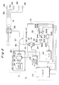
- Fig. 1 is a block diagram of a control system of optical lines facility which is applied to a method for identifying an optical line of this invention.
- Fig. 2 is a block diagram of an inner structure of a code reading device and its peripheral devices according to an embodiment of the first invention.
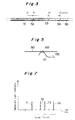
- Fig. 3 shows an example of an identification code.
- Fig. 4A and Fig. 4B show a method for converting an interferogram to a binary code information.
- Fig. 5 shows a branch optical line on which an identification code is formed.
- Fig. 6 is a block diagram of another structure of a code reading device.
- Fig. 7 is a graph of a detecting result.
- Fig. 8 is a block diagram of an inner structure of a code reading device and its peripheral devices according to embodiments of the second, third, and fourth invention.
- Fig. 9A shows an example of an identification code according to the embodiments of the second, third, and fifth invention.
- Fig. 9B shows an example of an identification code according to the embodiments of the second, third, and fifth invention.
- Fig. 10A is a graphic representation which shows a method for converting a reflected light to a binary code information according to the embodiments of the second and fifth invention.
- Fig. 10B is a table which shows a method for converting a reflected light to a binary code information according to the embodiments of the second and fifth invention.
- Fig. 11 shows a branch optical line on which an information code is formed.
- Fig. 12 is a block diagram of a structure of another code reading device according to the embodiments of the second, third and fourth invention.
- Fig. 13 is a perspective view of a structure of another reflecting part according to the embodiments of the second, third, fourth, and fifth invention.
- Fig. 14 is a perspective view of a structure of another reflecting part according to the embodiments of the second, third, fourth, and fifth invention.
- Fig. 15A is a graphic representation which shows a method for converting a reflected light spectrum to a quaternary code information according to the embodiment of the third invention.
- Fig. 15B is a table which shows a method for converting a reflected light spectrum to a quaternary code information according to the embodiment of the third invention.
- Fig. 16A is a perspective view which shows a method for writing down an identification code according to the embodiments of the second, third, fourth, and fifth invention.
- Fig. 16B is a perspective view which shows a method for writing down an identification code according to the embodiments of the second, third, fourth, and fifth invention.
- Fig. 16C is a perspective view which shows a method for writing down an identification code according to the embodiments of the second, third, fourth and fifth invention.
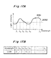
- Fig. 17A is a graphic representation which shows a method for converting a reflected light spectrum to a binary code information according to the embodiment of the fourth invention.
- Fig. 17B is a table which shows a method for converting a reflected light spectrum to a binary code information according to the embodiment of the fourth invention.
- Fig. 18 shows a block diagram of a code reading device and its peripheral devices according to the embodiment of the fifth invention.
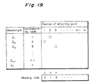
- Fig. 19 shows a method for converting a reflected light to a code information according to the embodiment of the fifth invention.
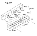
- Fig. 20 is a perspective view of an example of a code information according to an embodiment of the sixth invention.
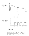
- Fig. 21A is a graphic representative which shows a method for converting a backscattering light intensity to a binary code information according to the embodiment of the sixth invention.
- Fig. 21B is a representative which shows a method for converting a backscattering light intensity to a binary code information according to the embodiment of the sixth invention.
- Fig. 21C is a table which shows a method for converting a backscattering light intensity to a binary code information according to the embodiment of the sixth invention.
- Fig. 22 is a block diagram of a code reading device and its peripheral devices according to the embodiment of the seventh invention.
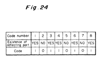
- Fig. 23 is a perspective view of an example of an identification code according to the embodiment of the seventh invention.
- Fig. 24 is a table which shows a method for converting existences of reflecting parts to a binary code information according to the embodiment of the seventh invention.
- Fig. 1 shows a structure of a control system of optical lines facility, which is applied to a method for identifying an optical line of this invention.
- a terminal 2 which switches the optical lines is placed between a local communication office 1 and a house of subscribers 3.
- a plurality of optical lines of which the one end is connected to a transmission device 4 inside of the office 1 are gathered as an optical fiber cable 9, and extend to the terminal 2.
- the other end of every optical line is connected to one end of a respective optical line extending to the house of subscribers 3 through an optical connector 10.
- the transmission device 4 inside of the office 1 and every house of subscribers 3 are substantially connected by one respective line.
- the optical connector 10 it can be freely operated by hand to switch connections. Before the switching is conducted, first, a route information of the optical lines is checked by an identifying method described thereinafter with a code reading device 5 placed inside of the office 1. Then, the route information is transmitted from a control device 6 to a local controller 11, and the information is given to an operator in the field through a display device 12. The operator conducts the requested connector switching based on the route information. After the switching is done, the route information is read again by the code reading device 5, and the route information is confirmed at the office 1 side. Then, this route information is displayed at the display device 12 through the control device 6 and the local controller 11, and the operator confirms the condition of the switching.
- Fig. 2 is a block diagram of an inner structure of the code reading device 5 and its peripheral devices.
- the code reading device 5 comprises a light emitting unit 20 and a light receiving unit 21, and they are controlled by a computer 22 and a timing control circuit 23 which form the control unit 6.
- the light emitting unit 20 contains a light source 24 for emitting a light having an appropriate spectrum range such as white ray, an acoustooptic element 25 for controlling an on/off of an irradiation of light from the light source 24, and lenses 26, 27 placed respectively at an input and an output of the acoustooptic element 25.
- a light emitted from the light source 24 is inputted to one end of the optical fiber 40 as a detecting light through the lens 26, the acoustooptic element 25 and the lens 27.
- the optical fiber 40 is a branch optical line which connects the optical fibers 50 as optical lines to be measured and the code reading device 5.
- the optical fiber 40 is connected to the optical lines 50 with a connecting means 38.
- the connecting means 38 alternatively connects the optical fiber 40 to one of the optical lines 50.
- the light receiving unit 21 contains a Michelson interferometer 30, an A/D convertor circuit 36 for converting an output signal from the Michelson interferometer 30 to a digital value and providing it to the computer 22, and an acoustooptic element 31 for controlling an on/off of an input light to the Michelson interferometer 30 based on a signal from the timing control circuit 23.
- the numerals 32, 33 denote lenses, and the numeral 34 denotes an optical fiber.
- the Michelson interferometer 30 contains a movable mirror 300, a fixed mirror 301, a beam splitter 302, a movable mirror moving device 303, a position-of-movable-mirror reading device 304, a light receiving element 305, and lenses 306, 307.
- a light inputted to the Michelson interferometer 30 from the optical fiber 34 is diverged by the beam splitter 302, and one is led to the fixed mirror 301 and the other one is led to the movable mirror 300.
- the lights reflected by the mirrors come back to the beam splitter 302, and interfere each other.
- the interference light is inputted to the light receiving element 305 through the lens 307 and is converted to an electrical signal.
- an interference waveform called an interferogram is obtained as the optical path length inside of the interferometer is varied by moving the movable mirror 300.
- This is a principle of operation of the Michelson interferometer 30. Using this principle, relative positions of the plurality of reflecting parts which form an identification code 39 are detected.
- Every optical line 50 has unique identification codes 39 written in.
- the identification code 39 consists of the plurality of reflecting parts, and each optical line has a different combination of relative positions of the reflecting parts.
- the reflecting parts forming the identification code 39 are notches on the optical line 50, which are discontinuous points of refractive indices.
- Fig. 3 shows an example of the identification code 39.
- the identification code 39 contains 4 notches 51-54, and the notches 52, 53, 54 are respectively at a distance of 3mm, 10mm and 15mm from the notch 51. Accordingly, if the detecting light from the light emitting unit 20 is inputted to the optical line 50, the reflected light arrived at the light receiving unit 21 from the identification code 39 includes optical path differences produced on the basis of distances between the notches. The optical path differences are detected by the Michelson interferometer 30, so that the relative positions of the notches 51-54 can be detected.
- the identification code 39 is applied to the optical lines between the local communication office 1 and the terminal 2, and to the optical lines between the terminal 2 and the houses of subscribers 3 as shown in Fig. 1. If there is a plurality of terminals between the office 1 and the houses 3, the identification code is also applied to the optical lines between the terminals.
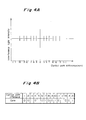
- the detecting light is inputted to the optical line 50 applied the identification code including the four reflecting parts 51-54 as shown in Fig. 3, the light receiving unit 21 collaborates with the computer 22 to get an interferogram shown in Fig. 4A.
- the sub interference intensities appear at the optical path difference of 3mm, 5mm, 7mm, 10mm, 12mm, and 15mm.
- Fig. 4B is a chart of an observational result corresponding to a code information.
- the 15 bits code information "001010100101001" is obtained from the observational result in Fig. 4A.
- the content of the code information is set freely as selecting a number of the reflecting parts or positions of the reflecting parts.
- the optical line which connects the office 1 and the house of subscribers 3 consists of two divided optical lines connected with the terminal 2. Since the identification code is applied to every divided optical line, they have to be distinguished and confirmed. For this reason, the acoustooptic element 31 is used.
- the pulsed detecting light is inputted to the optical line to be measured on the basis of the control of the timing control circuit 23, and based on the input timing of the detecting light, the reflected light from every identification code on the same optical line is periodically pick up by the acoustooptic element 31. Therefore, the reflected lights from the identification codes at different points on the same optical line is distinguished.
- the computer 22 distinguishes the reflected light from every identification code, it obtains a data of the light intensities of the reflected lights, and gets the interferogram of every identification code on the same optical line based on the input timing of the detecting light.
- Picking up the reflected light periodically can be achieved with an optical gate (optical deflector) instead of the acoustooptic element 31.
- a branch optical line 101 in which the identification code is written can be connected thereto with a fiber coupler 102 as shown in Fig. 5.
- Fig. 6 is a block diagram of a device for an identifying method according to another embodiment of the invention.
- the embodiment described above is to detect a relative positions of reflecting parts based on an interference of reflected lights.
- this embodiment is to detect a relative positions of reflecting parts by measuring an arrival time difference between reflected lights.
- a light emittig unit 20 contains a semiconductor laser 66 for outputting a pulse light having a short pulse-width, and a laser drive circuit 65.
- a light receiving unit 21 contains a light receiving element 61, an A/D convertor circuit 62 with memories, and an averaging circuit 63.
- the numerals 64 and 67 denote lenses respectively.
- a pulsed detecting light is inputted to the optical line 50, and a time variation in the reflected light intensities is measured, so that the code information corresponding to the relative positions of the reflecting parts can be read.
- Fig. 7 shows a graph of an example of a measurement result according to this embodiment. The ordinate indicates a reflected light intensity and the abscissa indicates a time.
- This example is to measure the reflected lights from the identification code having four reflecting parts including the reference reflecting part (the nearest reflecting part to the detecting light emitting side).
- the reflected light 71 from the reference reflecting part is arrived first, and the reflected lights 72, 73 and 74 are arrived in order of a distance close to the reference reflecting part. Assuming the reflecting parts except the reference reflecting part can be set only at five points equally separated, the 5 bits identification code can be made by existence of the reflecting part at the each point.
- the code information "01101" is indicated.
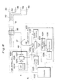
- FIG. 8 is a block diagram of an inner structure of a code reading device 5 and its peripheral devices in case that this embodiment applies to a control system of optical lines facility shown in Fig 1.
- a code reading device 5 contains a light emitting unit 1020 and a light receiving unit 1021, and they are controlled by a computer 1022 and a timing control circuit 1023 which form a control circuit 6.
- the light emitting unit 1020 contains a light source 1024 for emitting a light having an adequate spectrum range such as white ray, an acoustooptic element 1025 for controlling an on/off of a light outputted from the light source 1024, and lenses 1026, 1027 placed respectively at an input and an output of the acoustooptic element 1025.
- the light emitted from the light source 1024 is inputted to one end of an optical fiber 40 as a detecting light through the lens 1026, the acoustooptic element 1025, and the lens 1027.
- the optical fiber 40 is a branch optical line which connects optical fibers 50 to be measured and the code reading device 5.
- the optical fiber 40 is connected to the optical lines 50 with a connecting means 38.
- the connecting means 38 alternatively connects the optical fiber 40 to one of a plurality of the optical lines 50.
- the light receiving unit 1021 contains a Fabry-Perot etalon 1032 as an interference spectroscope, an etalon controller 1033 for controlling a space between two plane boards for a resonance in the etalon 1032, lenses 1030, 1031 placed respectively at an input and an output of the etalon 1032, a light receiving element 1034 for converting a light intensity of the output light from the etalon 1032 to an electrical signal, a boxcar integrator 1035 for periodically picking up an output signal from the light receiving element 1034 based on a signal from a timing control circuit 1023, and an A/D convertor circuit 1036 for converting an output of the boxcar integrator 1035 to a digital signal.
- a Fabry-Perot etalon 1032 as an interference spectroscope
- an etalon controller 1033 for controlling a space between two plane boards for a resonance in the etalon 1032
- lenses 1030, 1031 placed respectively at an input and an output of
- the etalon 1032 inputs a light from an optical fiber 41 connected to an optical fiber 40 with a fiber coupler 37 and analyzes spectra.
- the etalon controller 1033 controls a space between resonance planes in the etalon 1032 based on an instruction from a computer 1022.
- the computer 1022 obtains a data from the A/D convertor circuit 1036 with controlling the etalon 1032, it analyzes a wavelength of the reflected light.
- Each optical line 50 has unique identification codes 39 written in.
- the identification code consists of a plurality of reflecting parts.
- the each reflecting part reflect a light having a specific wavelength only.
- the optical line has a different combination of specific wavelengths of the reflecting parts each other.
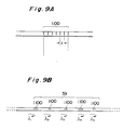
- Every reflecting part forming the identification code 39 is a striped pattern formed by varying the refractive index of the optical line 50 locally. As a spatial frequency of a variation of the refractive indices is adequately set, every reflecting part can obtain a unique wavelength of the reflected light. As shown in Fig. 9A, the reflecting part is the striped pattern where the refractive index is varied over a specific cycle.
- the reflecting parts 1100 obtained in such a way are set at plural points (in Fig. 9B, five points) on the optical line 50 as shown in Fig. 9B, and as the wavelengths ⁇ 1 - ⁇ 5 of the reflected lights are set adequately, the identification code can be formed.
- the refractive index can be varied permanently as a UV ray (Ultra Violet Ray) is partly irradiated to the optical line 50. By using this, the reflecting part which reflects a specific wavelength only can be formed.
- the identification code 39 is applied to the optical lines between the office 1 and the terminal 2, and to the optical lines between the terminal 2 and the houses of subscribers 3 as shown in Fig. 1. If there is a plurality of terminals between the office 1 and the houses of subscribers 3, the identification code is also applied to the optical lines between the terminals.
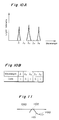
- Fig. 10A is a graph of an example of wavelength characteristics of the reflected lights when the detecting light from the light emitting unit 1020 is given to the optical line 50. The graph shows a wavelength on the abscissa and a light intensity on the ordinate. In this example, the reflected lights at wavelengths of ⁇ 1, ⁇ 3 and ⁇ 5 can be observed, and on the other hand, the reflected lights at wavelength of ⁇ 2 and ⁇ 4 cannot be observed.
- Fig. 10B is a chart of an observational result corresponded to the code information. A five bits code information "10101" is obtained from the result in Fig 10A.
- the optical line which connects the office 1 and the house of subscribers 3 consists of two divided optical lines connected with the terminal 2. Since the identification code is applied to every divided optical line, they have to be distinguished and confirmed. For this reason, the boxcar integrator 1035 is used. In other words, the pulsed detecting light is inputted to the optical line to be measured while the input timing is controlled by the timing control circuit 1023, and the reflected light from each identification code is periodically picked up based on the input timing of the detecting light. Therefore, the reflected lights from identification codes whose locations are different from each other on the same optical line can be distinguished.
- the computer 1022 distinguishes the reflected light from each identification code, it obtains a data of the reflected light intensities in correspondence with the wavelength, so that the computer gets the interferogram of each identification code.
- the distinction of reflected light can be achieved with an optical gate (optical deflector) instead of the boxcar integrator 1035.
- a branch optical line 1101 in which the identification code 1100 is written can be connected thereto with a fiber coupler 1102 as shown in Fig. 11.
- the white-light source 1024 is used as the light source, and the Fabry-Perot etalon 1032 is used as the spectroscope in the light receiving unit 1021.
- the spectroscope in the receiving unit 1021 can be omitted.
- the light source 1109 incorporates a semiconductor laser array 1110, a prism 1113, and a condenser lens 1027.
- the semiconductor laser array 1110 includes a plurality of the semiconductor lasers 1111 for emitting light of different wavelengths, and a lens 1112 which is placed at every semiconductor laser 1111.
- a control circuit 1114 controls a drive of the semiconductor laser 1111 and a movement of the prism 1113. Then, the light source 1109 can selectively outputs a detecting light having a required wavelength. The wavelength of the reflected light at every reflecting part is selected among the wavelengths emitted from the semiconductor lasers 1111. Accordingly, if the wavelength of the detecting light is subsequently switched and the existence of the reflected light at every wavelength is detected when the identification is conducted, similarly to the embodiment described above, the wavelength of the reflected light for every reflecting part can be obtained.
- the boxcar integrator 1035 is operated based on the timing signal from the control circuit 1114. But it is also possible that a light receiving element is placed at unused end of the optical fiber 41 to detect an input timing of the detecting light, and this detecting light is used as an operational timing signal for the boxcar integrator 1035.
- Fig. 13 is a perspective view of a structure of another example of a reflecting part used as an identification code 39.
- an optical filter is used as a reflecting part which reflects a specific wavelength only.
- a method for forming the identification code will be briefly explained.
- Two V-shaped notches 1201, 1202 are formed on a silicon board 1200, and core fibers 1204 and 1205 of a double core tape fiber 1203 which are optical lines are buried in respectively.
- a silicon lid is put over and is hardened with a resin 1207 to fix the optical fibers 1204 and 1205.
- a notch 1208 is formed on the silicon board 1200 over the silicon lid 1206, the optical fibers 1204 and 1205 are cut.
- a desired monochromatic reflecting optical filter 1210 is inserted in the notch 1208, so that the reflecting part which reflects a specific wavelength only is formed on the optical line.
- the optical filter 1210 is formed by a dielectric multiple layered film etc. Using the method with this optical filter, in case that the optical line is either a double core tape fiber like in this example or multicore tape fiber, it is possible to apply the same identification code to every optical fiber at the same time.
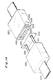
- Fig. 14 is a perspective view of an example of an optical filter placed in a connector.
- an optical line is formed as a plurality of divided optical fibers is connected by connectors.
- the optical filter which comprises an identification code is placed on one side of a connector, an installation of the optical filter becomes easy.
- the connector includes a male connector 1220 having a guide pin 1221, and a female connector 1223 having receiving holes for the guide pin 1221.
- Each connector 1220, 1223 has a structure that two silicon chips 1224, 1225 are piled and hardened with an epoxy resin 1226.
- a number of V-shaped notches equal to or larger than the number of optical fibers forming a tape fiber 1227 are placed on the silicon chip 1224, and each optical fiber is fixed in the V-shaped notch.
- the optical fibers on the side of the male connector 1220 and the optical fibers on the side of the female connector 1223 are coupled one by one.
- a monochromatic reflecting optical filter 1230 is inserted between them, so that the identification code can be formed on the optical line.
- the optical filter is made separately from the connectors 1220, 1223. But it is possible to form a dielectric multiple layered film on one side of the female connector 1223 by vapor-deposition.
- An identification code 39 consists of a plurality of reflecting parts.
- the each reflecting part reflect a light having a specific wavelength only.
- Each optical line has a different combination of specific wavelengths and reflectance.
- Every reflecting part forming the identification code 39 contains striped pattern where refractive indices are varied locally on the optical line 50.
- every reflecting part can obtain a unique wavelength of the reflected light and the reflectance.
- the reflecting part contains striped pattern where the refractive indices are varied over a specific cycle. Let a cycle of the striped pattern 1100 (i.e.
- the desired reflectance can be obtained by conducting the number of stripes and the difference of the refractive indices at striped pattern.
- the reflecting part 1100 obtained in such a way is set at plural parts (In Fig. 9B, five parts) on the optical line 50 as shown in Fig. 9B, and as the wavelengths ⁇ 1 - ⁇ 5 and the reflectances of the reflected lights are adequately set, the identification code can be formed.
- the refractive index can be varied as a UV ray (Ultra Violet Ray) is partly irradiated to the optical line. By using this, the reflecting part which reflects a light with a specific wavelength and reflectance only can be formed.
- the identification code 39 is applied to the optical lines between the office 1 and the terminal 2, and to the optical lines between the terminal 2 and the houses of subscribers 3 as shown in Fig. 1. If there is a plurality of terminals between the office 1 and the houses of subscribers 3, the identification code is also applied to the optical lines between the terminals.
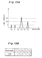
- a 4 notation number is coded. This means that if ⁇ 0 is a reflected wavelength at a reference reflecting part, and based on the reflected light intensity at the reference reflecting part, the other reflected lights with wavelengths ⁇ 1 - ⁇ 5 are corresponded to one of "0"-"3".
- Fig. 15A is a graph of an example of wavelength characteristics of the reflected lights when the detecting light from a light emitting unit 20 is given to the optical line 50. The graph shows a wavelength on the abscissa and a light intensity on the ordinate.
- Fig. 15B is a chart of an observational result corresponded to a code information.
- the code information "10302" is obtained from the result in Fig. 15B.
- the identification code on every divided optical line can be distinguished by the boxcar integrator 1035.
- the identification code can be written in a branch optical line as shown in Fig. 11.
- an embodiment according to a fourth invention is also applied to a control system of optical lines facility as shown in Fig. 1.
- An inner structure of a code reading device and its peripheral devices are shown in Fig. 8.
- an identification code 39 includes a reflecting part where the reflectance depend on wavelengths.
- the reflecting part contains striped pattern where the refractive indices are locally varied. As a spatial frequency of a variation of the refractive indices or a value of a refractive index is adequately set, the reflected light spectrum can be obtained.
- the reflected light spectrum is a content of the identification code 39.
- the identification code 39 is applied to the optical line between the office 1 and the terminal 2, and to the optical line between the terminal 2 and the houses of subscribers 3 as shown in Fig. 1. If there is a plurality of terminals between the office 1 and the houses of subscribers 3, the identification code is also applied to the optical lines between terminals.
- Fig. 16A-Fig. 16C show a method for writing reflecting parts which form an identification code 39. Every figure shows that as a UV ray (Ultra Violet Ray) is locally irradiated to the optical line 50 to vary a refractive index of the irradiated part, the reflecting part having a desired reflected light spectrum is formed.
- Fig. 16A shows a method for recording with a hologram. The UV ray 2062 is irradiated to the hologram 2061, and the diffracted lights by a hologram pattern recorded on the hologram 2061 are projected to the optical line 50.
- the refractive index is locally varied corresponding to a pattern formed by the diffracted lights, so that the reflecting part 2064 containing stripes of varied refractive index is formed on the optical line 50.
- the pattern made by the diffracted lights is freely set by changing a hologram pattern.
- Fig. 16B shows a method for forming a reflecting part 2074 having the striped pattern with the refractive index varied by condensing the UV ray 2072 with a lens 2073, and projecting a mask pattern 2071 having specific intervals and transmissivity of stripes to the optical line 50.
- Fig. 16C shows another method for forming a reflecting part having the striped pattern with the refractive index varied.
- This method comprises a control process of a UV ray intensity by forming a slit image with the UV ray 2083 on an optical line 50 using a slit 2081 and a lens 2082 and a control process of a movement of the slit image. While the UV ray intensity is adequately varied, the slit image is moved along the optical line 50 with a control of its speed to form the reflecting part.
- Fig. 17A is a graph of an example of a reflected light spectrum at an identification code 39 when the detecting light from a light emitted unit 1020 is given to the optical line 50.
- the abscissa indicates a wavelength and the ordinate indicates a light intensity.
- a threshold level 2092 is adequately set to the reflected light spectra 2091, and a binary code is applied to each wavelength based on whether the light intensity at each of wavelengths ⁇ 1 - ⁇ n is larger or smaller than the threshold level 2092.
- Fig. 17B shows a corresponding chart between the wavelengths and binary cords.
- the method for setting a threshold level 2092 is to set a light intensity at a specific wavelength of a reflected light as a threshold level 2092 other than the method for setting a threshold level in advance.
- the identification code on every divided optical line can be periodically picked up by the boxcar integrator 1035.
- the identification code can be written to a branch optical line as shown in Fig. 11.
- Fig. 18 is a block diagram of an inner structure of a code reading device 5 and its peripheral devices in case that this embodiment applies to a control system of optical lines facility shown in Fig. 1.
- the light emitting unit 3020 contains a light source 3109 and its drive control circuit 3114.
- the light source 3109 incorporates a semiconductor laser array 3110, a prism 3113, and a condenser lens 3027.
- the semiconductor laser array 3110 contains a plurality of semiconductor lasers 3111 which emit lights of different wavelengths, and a lens 3112 which is placed at every semiconductor laser 3111.
- the drive control circuit 3114 selectively controls a drive of the semiconductor laser 3111 and a movement of the prism 3113, so that the light source 3109 can selectively output a detecting light having a required wavelength.
- An optical fiber 40 is a branch optical line which connects optical fibers 50 to be measured and a code reading device 5, and is connected to the optical fibers 50 to be measured with a connecting means 38.
- the connecting means 38 selectively connects the optical fiber 40 to one of the optical lines 50 to be measured.
- a light receiving unit 3021 contains a light receiving element 3034 for converting an inputted light to an electrical signal, and an A/D convertor circuit 3035 with memories for converting a signal from the light receiving element 3034 to a digital value, and an averaging circuit 3036 for averaging the digital value from the A/D convertor circuit 3035.
- An optical fiber 41 is connected to the optical fiber 40 with an optical fiber coupler 37, and one end is led to the light receiving unit 3021.
- the A/D convertor circuit 3035 stores a time variation in signals from the light receiving element 3034 based on the emitting timing of the detecting light from the drive control circuit 3114 and converts an analog data to a digital data in an appropriate interval. Accordingly, a period from time when the light emitting unit 3020 emits the detecting light to time when the reflected light comes back can be detected.
- a computer 3022 can identify a specific wavelength of every reflecting part which forms an identification code 39 and a relative position thereof, using a combination of the wavelength of a detecting light and the time when the reflected light at the identification code 39 arrives.
- Each optical line 50 has unique identification codes 39 written in.
- the identification code 39 consists of a plurality of reflecting parts. Each reflecting part reflects a light having a specific wavelength only. Each optical line has a different combination of specific wavelengths and relative positions of reflecting parts. Every reflecting part forming the identification code 39 contains striped pattern where refractive indices are varied locally on the optical line 50. As a spatial frequency of a variation of the refractive indices etc. are adequately set, every reflecting part can obtain a unique wavelength of the reflected light. As shown in Fig. 9A, the reflecting part contains striped pattern where the refractive indices are varied over a specific cycle. Let a cycle of the striped pattern 1100 (i.e.
- the reflecting part 1100 obtained in such a way is set at plural parts (In Fig. 9B, 5 parts) on the optical line 50 as shown in Fig. 9B, and as the wavelengths ⁇ 1 - ⁇ 5 of the reflected lights and relative positions of the reflecting parts are set adequately, the identification code can be formed.
- the refractive index can be varied as a UV ray (Ultra Violet Ray) is locally irradiated to the optical line 50. By using this, the reflecting part which reflects a specific wavelength only is formed.
- the identification code 39 is applied to the optical lines between the office 1 and the terminal 2, and to the optical lines between the terminal 2 and the houses of subscribers 3 as shown in Fig. 1. If there is a plurality of terminals between the office 1 and the houses of subscribers 3, the identification code is also applied to the optical lines between the terminals.
- n notation number is coded with n kinds of wavelengths ⁇ 1 - ⁇ n as wavelengths of reflected lights. This means that numbers 1 to n are assigned to every wavelength. Then, a reflecting part having a wavelength characteristic selected from these wavelengths is applied to m points of the optical line 50. Accordingly, the n notation number of m figure can be coded with the specific wavelengths of the reflecting parts and their relative positions. Since the code reading device 5 can detect the wavelength of the detecting light and the arrival time of the reflected light, the code can be read.
- Fig. 19 shows a combination chart of wavelengths and the relative positions of the reflecting parts. This chart indicates that the wavelength ⁇ 2 is formed first, ⁇ 1 is a second, ⁇ 3 is a third and so on, and as reading this and converting it to a code, "213 ... " is made.
- the A/D convertor circuit 3035 is driven based on the timing signal from the drive control circuit 3114, but it is possible that with the light receiving element placed at unused end of the optical fiber 41, the input timing of the detecting light is detected, and this detected signal is used as an operational timing signal for the A/D convertor circuit 3035.
- the identification code can be written in a branch optical line as shown in Fig. 11.
- a code reading device shown in Fig. 6 is applied to the system shown in Fig. 1.
- Each optical line 50 has unique identification codes 39 written in.
- the identification code 39 consists of a plurality of bending loss parts. A combination of relative positions of the bending loss parts is changed for each optical line. Every bending loss part forming the identification code 39 is a bending part on the optical line 50, and a concrete example of a jig is shown in Fig. 20.
- the jig 4080 consists a receiving member 4081 with V-shaped notches and a weight member 4082. In the receiving member 4081, concavities are formed at the V-shaped notches corresponding to a required identification code.
- the concavities 4083-4086 are formed in the first, third, fourth, and seventh notch.
- projections 4087-4090 are formed at the position corresponding to the concavities on the receiving member 4081.
- the optical line 50 is meandered and inserted in the V-shaped notches on the receiving member 4081 and weighted over with the weight member 4082, so that the bending loss parts are formed at the first, third, fourth, and seventh V-shaped notch.
- a pulsed detecting light is inputted to the optical line 50, and a time variation in backscattering light intensities is measured, so that a code information corresponding to a relative position of each bending loss part is read.
- the identification code 39 is applied to the optical lines between the office 1 and the terminal 2, and to the optical lines between the terminal 2 and the houses of subscribers 3 as shown in Fig. 1. If there is a plurality of terminals between the office 1 and the houses of subscribers 3, the identification code is also applied to the optical lines between the terminals.
- a method for reading an identification code 39 in this embodiment will be explained.
- a detecting light is inputted to the optical line 50 having the identification code formed with the four bending loss parts as shown in Fig. 20.
- the light receiving unit 21 collaborates with the computer 22 to obtain a characteristic of a time variation in the backscattering light intensities as shown in Fig. 21A. This means that at the each bending loss part, the backscattering light intensity rapidly decreases based on the irradiation loss.
- Fig. 21B shows a result of the differentiated characteristics. In this graph, peaks 4095, 4096, 4097 and 4098 are corresponding to the first, third, fourth and seventh bending loss part formed in the V-shaped notches.
- the characteristics shown in Fig. 21B can be replaced with a seven bits code shown in Fig. 21C.
- the content of the code information is set freely as selecting a number of the bending loss parts or positions of the bending loss parts.
- the optical line which connects the office 1 and the houses 3 of subscribers consists of two divided optical lines connected with the terminal 2. Since the identification code is applied to every divided optical line, they have to be distinguished and confirmed. In order to do that, as an operation of the A/D convertor circuit 62 with memories is periodically controlled by timing control circuit 23, a variation of the light intensities is periodically picked up based on the input timing of the detecting light. Therefore, the variation of the light intensities at different points of the identification code on the same optical line can be distinguished. Picking up the backscattering light can be achieved with an optical gate (optical deflector). As shown in Fig. 11, the identification code can be written in a branch optical line.
- a code reading device shown in Fig. 22 is applied to the system shown in Fig. 1.
- optical lines between the office 1 and terminal 2 are gathered to be a multicore optical line, and further the multicore optical lines are gathered to be an optical fiber 9.
- the identification of the optical line described thereinafter is related to an identification of a multicore optical line.
- each mono-optical line inside of the multicore optical line is called a core optical fiber.
- Fig. 22 shows a block diagram of an inner structure of a code reading device 5 and its peripheral devices.
- a code reading device 5 consists of a light emitting unit 5020 and a light receiving unit 5021, and they are controlled by a computer 5022 and a timing control circuit 5023 which form a control circuit 6.
- the light emitting unit 5020 contains a light source 5024 for emitting a light having an adequate spectrum range such as white ray, an acoustooptic element 5025 for controlling an on/off of a light outputted from the light source 5024, and lenses 5026, 5027 placed respectively at an input and an output of the acoustooptic element 5025.
- the light emitted from the light source 5024 is inputted to one end of an optical fiber 40 as a detecting light through the lens 5026, the acoustooptic element 5025, and the lens 5027.
- the optical fiber 40 is a branch optical line which connects one of the multicore optical lines 50 to be measured and the code reading device 5.
- the optical fiber 40 is connected to the multicore optical line 50 with a connecting means 38.
- the optical fiber 40 is also a multicore optical fiber having a number of cores equal to the number of core fibers of optical line 50.
- the connecting means 38 alternatively connects the multicore optical fiber 40 to one of a plurality of the multicore optical lines 50 to be measured.
- a light receiving unit 5021 contains a number of light receiving elements 5031 equal to the number of core fibers of the multicore optical line for converting an inputted light to an electrical signal, and an A/D convertor circuit 3035 for converting a signal from the light receiving element 5031 to a digital value and transmitting the digital value to a computer 5022, and a lens 5033 placed in front of every light receiving element 5031.
- the light receiving element 5031 receives a light from an optical fiber 41 connected to an optical fiber 40 with a fiber coupler 37 and converts the light to an electrical signal.
- the optical fiber 41 is also a multicore optical fiber having a number of optical core fibers equal to the number of core fibers of a multicore optical line 50 that is the number of core fibers of the optical fiber 40.
- Each core optical fiber of the optical fiber 41 is led to the light receiving element 5031. Accordingly, the existence of the reflected light at every core optical fiber can be detected.
- the light receiving elements 5031 are controlled by the timing control circuit 5023, and the light receiving element is operated subsequently from the left hand of the figure, so that the reflected light at the each core optical fiber is subsequently provided to the A/D convertor circuit 5032.
- Unique identification codes 39 are written in each optical line 50.
- the identification code is formed by placing reflecting parts selectively on core optical fibers of the multicore optical line and changing a combination of the existence of the reflecting part at the core optical fibers for every multicore optical line.
- Fig. 23 shows an example of the identification code at the multicore tape optical line.
- Each core optical fiber 5061 of the multicore tape optical line 5060 is exposed to be a part on which the identification code will be made.
- the reflecting part 5063 is selectively made at this part.
- the reflecting parts 5063 can be formed as the refractive indices are varied by irradiating to the core optical lines 5061 with a UV ray (Ultra Violet Ray).
- the reflecting parts 5063 can be also formed by cutting the core optical fibers and inserting an optical filter into the cutting part.
- identification code part 5063 remains being exposed for easy explanation. This part will be fixed by a board like a silicon chip to maintain a mechanical strength in practice.
- a multicore optical line is 8-core tape optical fiber.
- the receiving unit 5021 receives only a reflected light from the core optical fiber having a reflected part. These reflected light is detected at the light receiving element 5031 corresponding to the core optical fiber one by one, and the signal is inputted to the computer 5022 through the A/D convertor circuit 5032.
- Fig. 24 shows a chart of a detection result. All core optical fibers are numbered 1-8. By the existence of the reflecting part at the each numbered core optical fiber, the detection of the reflected light is made. When the reflected light is detected, a code "1" is given and when the reflected light is not detected, a code "0" is given, so that the 8 bits code information is obtained from the detecting result.
- the identification code can be written to a branch optical line.
- the optical line is a multicore type
- reflecting parts can be selectively applied to core optical lines to form an identification code.
- the multicore optical line can be easily and accurately identified.
Landscapes
- Physics & Mathematics (AREA)
- General Physics & Mathematics (AREA)
- Optics & Photonics (AREA)
- Engineering & Computer Science (AREA)
- Chemical & Material Sciences (AREA)
- Analytical Chemistry (AREA)
- Computer Networks & Wireless Communication (AREA)
- Electromagnetism (AREA)
- Manufacturing & Machinery (AREA)
- Signal Processing (AREA)
- Light Guides In General And Applications Therefor (AREA)
- Optical Communication System (AREA)
- Length Measuring Devices By Optical Means (AREA)
- Glass Compositions (AREA)
- Sampling And Sample Adjustment (AREA)
- Diffracting Gratings Or Hologram Optical Elements (AREA)
Claims (33)
- Verfahren zum Identifzieren einer optischen Leitung, umfassend die folgenden Schritte:Bilden einer Vielzahl von reflektierenden Teilen auf einer optischen Leitung entlang einer Längsrichtung davon;Identifizieren der optischen Leitung auf Grundlage einer Kombination von Information in dem Licht, das von den reflektierenden Teilen zurückkommt.
- Verfahren zum Identifizieren einer optischen Leitung nach Anspruch 1, umfassend die folgenden Schritte:Bilden der Vielzahl der reflektierenden Teile auf der jeden optischen Leitung als einen Identifikationscode, wobei die jede optische Leitung eine spezifische Kombination von relativen Positionen der reflektierenden Teile aufweist;Erfassen der relativen Positionen der reflektierenden Teile auf Grundlage von reflektiertem Licht, wenn ein Erfassungslicht der optischen Leitung eingegeben wird; undIdentifizieren der optischen Leitung auf Grundlage eines Ergebnisses des Erfassungsschrittes.
- Verfahren zum Identifizieren einer optischen Leitung nach einem der vorangehenden Ansprüche, umfassend die folgenden Schritte:Bilden der Vielzahl der reflektierenden Teile auf der jeden optischen Leitung als einen Identifikationscode, wobei jedes reflektierende Teil Licht mit einer spezifischen Wellenlänge reflektiert und wobei die jede optische Leitung eine spezifische Kombination der spezifischen reflektierenden Wellenlängen aufweist;Erfassen von Wellenlängen des reflektierten Lichts, wenn ein Erfassungslicht der optischen Leitung eingegeben wird; undIdentifizieren der optischen Leitung auf Grundlage eines Ergebnisses des Erfassungsschrittes.
- Verfahren zum Identifizieren einer optischen Leitung nach einem der vorangehenden Ansprüche, umfassend die folgenden Schritte:Bilden der Vielzahl der reflektierenden Teile auf der jeden optischen Leitung als einen Identifikationscode, wobei jedes reflektierende Teil Licht mit einer spezifischen Wellenlänge reflektiert und wobei die jede optische Leitung eine spezifische Kombination der spezifischen reflektierenden Wellenlängen und der Reflektivität aufweist;Erfassen von Wellenlängen und der Reflektivität des reflektierten Lichts, wenn ein Erfassunglicht der optischen Leitung eingegeben wird; undIdentifizieren der optischen Leitung auf Grundlage eines Ergebnisses des Erfassungsschritts.
- Verfahren zum Identifizieren einer optischen Leitung nach einem der vorangehenden Ansprüche, umfassend die folgenden Schritte:Bilden der Vielzahl der reflektierenden Teile auf der jeden optischen Leitung als einen Identifikationscode, wobei jedes reflektierende Teil Licht mit einer spezifischen Wellenlänge reflektiert und wobei die jede optische Leitung eine spezifische Kombination der spezifischen reflektierenden Wellenlängen und relativen Positionen aufweist;Erfassen von Wellenlängen und relativen Positionen des reflektierten Lichts, wenn ein Erfassunglicht der optischen Leitung eingegeben wird; undIdentifizieren der optischen Leitung auf Grundlage eines Ergebnisses des Erfassungsschrittes.
- Verfahren zum Identifizieren einer optischen Leitung nach einem der vorangehenden Ansprüche, umfassend die folgenden Schritte:Bilden des reflektieren Teils auf der jeden optischen Leitung als ein Identifikationscode, wobei das reflektierende Teil auf der jeden optischen Leitung eine spezifische Reflektivitätscharakteristik in Abhängigkeit von einer Wellenlänge aufweist;Erfassen eines Reflektionslichtspektrums, das von einem reflektierenden Teil zurückkommt, wenn ein Erfassungslicht der optischen Leitung eingegeben wird; undIdentifizieren der optischen Leitung auf Grundlage eines Ergebnisses des Erfassungsschrittes.
- Verfahren zum Identifizieren einer optischen Leitung nach einem der vorangehenden Ansprüche,
dadurch gekennzeichnet, daß
die mehreren reflektierenden Teile auf jeder optischen Zweigleitung vorgesehen sind. - Verfahren zum Identifizieren einer optischen Leitung nach einem der vorangehenden Ansprüche, gekennzeichnet durch den folgenden Schritt:
Erfassen der Information des reflektierten Lichts, das von dem reflektierenden Teil zurückkommt, zu einem Zeitpunkt in Abhängigkeit von der Position davon, wenn ein gepulstes Erfassungslicht der optischen Leitung eingegeben wird. - Verfahren zum Identifizieren einer optischen Leitung nach einem der vorangehenden Ansprüche,
dadurch gekennzeichnet, daß:
das reflektierende Teil aus einem Streifenmuster besteht und durch Ändern des Brechungsindex in der optischen Leitung oder der optischen Zweigleitung lokal gebildet ist. - Verfahren zum Identifizieren einer optischen Leitung nach einem der vorangehenden Ansprüche,
dadurch gekennzeichnet, daß
das reflektierende Teil eine optische Faser ist, die in die optische Leitung oder optische Zweigleitung eingefügt ist. - Verfahren zum Identifizieren einer optischen Leitung nach einem der vorangehenden Ansprüche,
dadurch gekennzeichnet, daßdie optische Leitung aus einer Vielzahl von geteilten optischen Fasern besteht;ein Verbindungsteil mit einem optischen Verbinder zwischen den geteilten optischen Leitungen vorgesehen ist; undein optisches Filter als das Reflektionsteil an dem optischen Verbinder gebildet ist. - Verfahren zum Identifizieren einer optischen Mehrkernleitung bestehend aus einem Bündel von optischen Kernleitungen, umfassend die folgenden Schritte:Bilden einer Vielzahl von reflektierenden Teilen auf der optischen Mehrkernleitung davon selektiv als einen Identifikationscode;wobei die optische Mehrkernleitung eine spezifische Kombination von Existenzen der reflektierenden Teile und Charakteristiken von Reflektionen aufweist;Erfassen des Lichts, das von den reflektierten Teilen zurückkommt, wenn Erfassungslicht der optischen Mehrkernleitung eingegeben wird;Identifizieren der optischen Mehrkernleitung auf Grundlage eines Ergebnisses des Erfassungsschritts.
- Verfahren zum Identifizieren einer optischen Leitung nach einem der Ansprüche 1-12
dadurch gekennzeichnet, daß
eine optische Pfaddifferenz des reflektierten Lichts von den reflektierenden Teilen durch ein Interferrometer gemessen wird und die relativen Positionen der reflektierenden Teile auf Grundlage eines Ergebnisses der Messung erfaßt werden. - Verfahren zum Identifizieren einer optischen Leitung, umfassend die folgenden Schritte:Bilden einer Vielzahl von Biegeverlustteilen auf einer optischen Leitung als einen Identifikationscode entlang einer Längsrichtung davon, wobei die Biegeverlustteile eine spezifische Kombination von relativen Positionen aufweisen;Erfassen der relativen Positionen der Vielzahl von Biegeverlustteilen auf Grundlage des von der Vielzahl von Biegeverlustteilen zurückgestreuten Lichts, wenn ein Erfassungslicht der optischen Leitung eingegeben wird; undIdentifizieren der optischen Leitung auf Grundlage eines Ergebnisses des Erfassungsschritts.
- Verfahren nach den Ansprüchen 1-13,
dadurch gekennzeichnet, daßdie reflektierenden Teile jeweils als ein Beugungsgitter (2064) auf einer optischen Leitung (50) gebildet werden, umfassend die folgenden Schritte:Bereitstellen einer optischen Leitung (50);Strahlen eines Lichts (2062) auf die optische Leitung (50) durch ein Hologrammuster (2061), um so Beugungslicht, verursacht durch das Hologrammuster, auf die optische Leitung (50) zu projezieren, um dadurch Bereiche (2064) zu bilden, deren Brechungsindex einer Intensität des auf die optische Leitung (50) zu projezierenden, gebrochenen Lichts entspricht. - Verfahren nach Anspruch 15,
dadurch gekennzeichnet, daß
das Licht, das auf das Hologrammuster gestrahlt wird, ein ultravioletter Strahl ist, - Verfahren nach Anspruch 15 oder 16,
dadurch gekennzeichnet, daß
die optische Leitung (50) eine optische Faser umfaßt. - Optische Leitung mit einer Vielzahl von entlang einer Längsrichtung davon gebildeten Reflektionsteilen zum Identifizieren der optischen Leitung auf Grundlage einer Kombination von Information in dem Licht, das von den reflektierenden Teilen zurückkommt.
- Optische Leitung (50) nach Anspruch 18 mit wenigstens einem Beugungsgitterbereich als das Reflektionsteil, wobei der Beugungsgitterbereich (2064) durch Strahlen von Licht durch ein Hologrammuster (2061), um so ein Beugungslicht (2063), verursacht durch das Hologrammuster, auf die optische Leitung (50) zu projezieren, gebildet ist, wobei ein Brechungsindex des Beugungsgitterbereichs einer Intensität des Beugungslichts entspricht.
- Verfahren nach den Ansprüchen 1-13
dadurch gekennzeichnet, daßdie reflektierenden Teile jeweils als ein Beugungsgitter auf einer optischen Leitung (50) gebildet sind, umfassend die folgenden Schritte:Bereitstellen einer optischen Leitung (50); undStrahlen eines Lichts (2072) auf ein Maskenmuster (2071) einschließlich einer Vergrößerung eines Lichtmusters, das durch das Maskenmuster tritt, unter Verwendung eines optischen Systems (2073), um dadurch das vergrößerte Lichtmuster auf die optische Leitung zu projezieren, wobei ein Brechungsindex des Bereichs (2074) einer Intensität des durch das Maskenmuster (2071) tretenden Lichtmusters entspricht. - Verfahren nach Anspruch 20,
dadurch gekennzeichnet, daß
das optische System (2073), das in dem Vergrößerungsschritt verwendet wird, eine Linse (2073) umfaßt. - Verfahren nach Anspruch 20,
dadurch gekennzeichnet, daß
das auf das Maskenmuster (2071) gestrahlte Licht ein ultravioletter Strahl ist. - Verfahren nach Ansprch 20,
dadurch gekennzeichnet, daß
die optische Leitung (50) eine optische Faser umfaßt. - Optische Leitung nach Anspruch 18 mit wenigstens einem Beugungsgitterbereich als das Reflektionsteil, wobei der Beugungsgitterbereich durch Strahlen von Licht (2072) auf ein Maskenmuster (2071), um ein durch das Maskenmuster (2071) tretendes Lichtmuster mit einem optischen System (2073) zu vergrößern, gebildet wird, um dadurch ein vergrößertes Lichtmuster auf die optische Leitung (50) zu projezieren, wobei ein Brechungsindex des Beugungsgitterbereichs (2074) einer Intensität des durch das Maskenmuster (2071) tretenden Lichtmusters entspricht.
- Verfahren nach den Ansprüchen 1-13,
dadurch gekennzeichnet, daßdie reflektierenden Teile jeweils als ein Beugungsgitter auf einer optischen Leitung (50) gebildet sind, umfassend die folgenden Schritte:Bereitstellen einer optischen Leitung (50);Strahlen von Licht (2083) durch einen Schlitz (2081) zum Projezieren eines Schlitzabbildes auf die optische Leitung mit Ändern einer Intensität des Lichts, das gerade aufgestrahlt wird, gemäß einer Funktion einer Projektionsposition des Schlitzabbildes in einer Längsrichtung (2084) der optischen Leitung, um einen Bereich mit einem Brechungsindex zu bilden, der sich von demjenigen der Umgebung davon unterscheidet. - Verfahren nach Anspruch 25,
dadurch gekennzeichnet, daß
das Licht, das durch den Schlitz (2081) gestrahlt wird, ein ultravioletter Strahl ist. - Verfahren nach Anspruch 25,
dadurch gekennzeichnet, daß
die optische Leitung eine optische Faser umfaßt. - Verfahren nach Anspruch 25,
dadurch gekennzeichnet, daß
das Gitter durch die Kombination einer Intensitätssteuerung von UV-Licht und durch eine Bewegungssteuerung des Schlitzes gebildet wird. - Optische Leitung nach Anspruch 18 mit wenigstens einem Beugungsgitterbereich als das Reflektionsteil, wobei der Beugungsgitterbereich durch Strahlen eines Lichts (2083) durch einen Schlitz (2081), um so ein Schlitzabbild auf die optische Leitung zu projezieren, gebildet wird, wobei eine Intensität des Lichts, das gerade aufgestrahlt wird, gemäß einer Funktion der Projektionsposition des Schlitzabbildes entlang einer Längsrichtung (2084) der optischen Leitung geändert wird, um dadurch einen Bereich mit einem Brechungsindex zu bilden, der sich von demjenigen der Umgebung davon unterscheidet.
- Optische Leitung nach Anspruch 19,
dadurch gekennzeichnet, daß
eine Vielzahl von Beugungsgitterbereichen auf der optischen Leitung vorgesehen sind und entlang einer Längsrichtung der optischen Leitung angeordnet sind, wodurch die optische Leitung mit wenigstens einer Charakteristik eines Lichts, das von der Vielzahl von Beugungsgitterbereichen im Ansprechen auf Licht, das an ein Ende der optischen Leitung geführt wird, reflektiert wird, identifiziert werden kann. - Optische Leitung nach Anspruch 24,
dadurch gekennzeichnet, daß
eine Vielzahl von Beugungsgitterbereichen auf der optischen Leitung vorgesehen sind und entlang einer Längsrichtung angeordnet sind, wobei die optische Leitung mit wenigstens einer Charakteristik von Licht, das von der Vielzahl von Beugungsgitterbereichen im Ansprechen auf Licht, das an ein Ende der optischen Leitung geführt wird, identifiziert werden kann. - Optische Leitung nach Anspruch 29,
dadurch gekennzeichnet, daß
eine Vielzahl von Beugungsgitterbereichen auf der optischen Leitung vorgesehen sind und entlang einer Längsrichtung angeordnet sind, wobei die optische Leitung gemäß wenigstens einer Charakteristik von Licht, das von den Beugungsgitterbereichen im Ansprechen auf Licht, das an ein Ende der optischen Faser geführt wird, reflektiert wird, identifiziert werden kann. - Verfahren nach Anspruch 12,
dadurch gekennzeichnet, daß
die Vielzahl von reflektierenden Teilen auf der optischen Mehrkernleitung entlang einer Längsrichtung davon gebildet sind.
Priority Applications (1)
| Application Number | Priority Date | Filing Date | Title |
|---|---|---|---|
| EP98102083A EP0851248B1 (de) | 1992-05-01 | 1993-04-28 | Verfahren zur Identifikation einer optischen Leitung |
Applications Claiming Priority (15)
| Application Number | Priority Date | Filing Date | Title |
|---|---|---|---|
| JP04112805A JP3078104B2 (ja) | 1992-05-01 | 1992-05-01 | 光線路の識別方法 |
| JP04112818A JP3078105B2 (ja) | 1992-05-01 | 1992-05-01 | 光線路の識別方法 |
| JP4112797A JPH05307118A (ja) | 1992-05-01 | 1992-05-01 | 光線路の識別方法 |
| JP112818/92 | 1992-05-01 | ||
| JP112822/92 | 1992-05-01 | ||
| JP04112822A JP3078106B2 (ja) | 1992-05-01 | 1992-05-01 | 光線路の識別方法 |
| JP112808/92 | 1992-05-01 | ||
| JP04112804A JP3078103B2 (ja) | 1992-05-01 | 1992-05-01 | 光線路の識別方法 |
| JP112820/92 | 1992-05-01 | ||
| JP112804/92 | 1992-05-01 | ||
| JP04112808A JP3129831B2 (ja) | 1992-05-01 | 1992-05-01 | 光線路の識別方法 |
| JP112805/92 | 1992-05-01 | ||
| JP112797/92 | 1992-05-01 | ||
| JP4112820A JPH05313020A (ja) | 1992-05-01 | 1992-05-01 | 光線路の識別方法 |
| PCT/JP1993/000567 WO1993022647A1 (en) | 1992-05-01 | 1993-04-28 | Method for identifying optical line |
Related Child Applications (1)
| Application Number | Title | Priority Date | Filing Date |
|---|---|---|---|
| EP98102083A Division EP0851248B1 (de) | 1992-05-01 | 1993-04-28 | Verfahren zur Identifikation einer optischen Leitung |
Publications (3)
| Publication Number | Publication Date |
|---|---|
| EP0592690A1 EP0592690A1 (de) | 1994-04-20 |
| EP0592690A4 EP0592690A4 (de) | 1995-03-15 |
| EP0592690B1 true EP0592690B1 (de) | 1998-10-14 |
Family
ID=27565796
Family Applications (2)
| Application Number | Title | Priority Date | Filing Date |
|---|---|---|---|
| EP98102083A Expired - Lifetime EP0851248B1 (de) | 1992-05-01 | 1993-04-28 | Verfahren zur Identifikation einer optischen Leitung |
| EP93911952A Expired - Lifetime EP0592690B1 (de) | 1992-05-01 | 1993-04-28 | Verfahren zur identifizierung einer optischen linie |
Family Applications Before (1)
| Application Number | Title | Priority Date | Filing Date |
|---|---|---|---|
| EP98102083A Expired - Lifetime EP0851248B1 (de) | 1992-05-01 | 1993-04-28 | Verfahren zur Identifikation einer optischen Leitung |
Country Status (9)
| Country | Link |
|---|---|
| US (2) | US5506674A (de) |
| EP (2) | EP0851248B1 (de) |
| KR (2) | KR970004993B1 (de) |
| CN (2) | CN1238980C (de) |
| AU (1) | AU666382B2 (de) |
| CA (1) | CA2112692C (de) |
| DE (2) | DE69333369T2 (de) |
| NO (1) | NO318903B1 (de) |
| WO (1) | WO1993022647A1 (de) |
Cited By (3)
| Publication number | Priority date | Publication date | Assignee | Title |
|---|---|---|---|---|
| GB2280326B (en) * | 1993-07-15 | 1997-04-23 | Marconi Gec Ltd | Optical communication systems |
| FR2865044A1 (fr) * | 2004-01-14 | 2005-07-15 | Cit Alcatel | Fibre optique facilement identifiable, procedes d'identification et de fabrication d'une telle fibre optique |
| US7974182B2 (en) | 2004-03-31 | 2011-07-05 | British Telecommunications Public Limited Company | Evaluating the position of a disturbance |
Families Citing this family (79)
| Publication number | Priority date | Publication date | Assignee | Title |
|---|---|---|---|---|
| GB9506163D0 (en) * | 1995-03-27 | 1995-05-17 | Bicc Plc | Optical fibre and network |
| GB9515498D0 (en) * | 1995-07-28 | 1995-09-27 | Bicc Plc | Optical fibre system |
| JP2924881B2 (ja) * | 1997-01-27 | 1999-07-26 | 住友電気工業株式会社 | 波長可変光源およびotdr装置 |
| US5898804A (en) * | 1997-06-09 | 1999-04-27 | Trw Inc. | Precision wavelength control for automated fiber optic Bragg grating writing |
| JP3414257B2 (ja) * | 1998-05-19 | 2003-06-09 | 安藤電気株式会社 | 多心光ファイバの測定データ集計方法及び装置ならびに集計処理プログラムを記録した記録媒体 |
| US6157443A (en) * | 1998-08-19 | 2000-12-05 | Lucent Technologies Inc. | Method and system for transporting data for monitoring optical fibers |
| US20050074244A1 (en) * | 2000-01-12 | 2005-04-07 | Nortel Networks Limited | Optimization of a communications system based on identification of an optical member |
| US6347172B1 (en) | 2000-06-28 | 2002-02-12 | Alcatel | Cable having side-emitting fiber under transparent or translucent cable jacket |
| US6643436B2 (en) * | 2000-12-14 | 2003-11-04 | Radiodetection Limited | Identifying fibers of fiber optic cables |
| US7508608B2 (en) * | 2004-11-17 | 2009-03-24 | Illumina, Inc. | Lithographically fabricated holographic optical identification element |
| US7399643B2 (en) * | 2002-09-12 | 2008-07-15 | Cyvera Corporation | Method and apparatus for aligning microbeads in order to interrogate the same |
| EP1535241A1 (de) * | 2002-08-20 | 2005-06-01 | Cyvera Corporation | Auf einem beugungsgitter basierendes optisches identifikationselement |
| US7901630B2 (en) | 2002-08-20 | 2011-03-08 | Illumina, Inc. | Diffraction grating-based encoded microparticle assay stick |
| US7872804B2 (en) * | 2002-08-20 | 2011-01-18 | Illumina, Inc. | Encoded particle having a grating with variations in the refractive index |
| US20050227252A1 (en) * | 2002-08-20 | 2005-10-13 | Moon John A | Diffraction grating-based encoded articles for multiplexed experiments |
| US7923260B2 (en) | 2002-08-20 | 2011-04-12 | Illumina, Inc. | Method of reading encoded particles |
| US7164533B2 (en) | 2003-01-22 | 2007-01-16 | Cyvera Corporation | Hybrid random bead/chip based microarray |
| US7619819B2 (en) | 2002-08-20 | 2009-11-17 | Illumina, Inc. | Method and apparatus for drug product tracking using encoded optical identification elements |
| US7441703B2 (en) * | 2002-08-20 | 2008-10-28 | Illumina, Inc. | Optical reader for diffraction grating-based encoded optical identification elements |
| US7900836B2 (en) | 2002-08-20 | 2011-03-08 | Illumina, Inc. | Optical reader system for substrates having an optically readable code |
| AU2003265584C1 (en) * | 2002-08-20 | 2009-05-21 | Cyvera Corporation | Diffraction grating-based encoded micro-particles for multiplexed experiments |
| CA2498916A1 (en) * | 2002-09-12 | 2004-03-25 | Cyvera Corporation | Chemical synthesis using diffraction grating-based encoded optical elements |
| US20100255603A9 (en) | 2002-09-12 | 2010-10-07 | Putnam Martin A | Method and apparatus for aligning microbeads in order to interrogate the same |
| CA2498906A1 (en) * | 2002-09-12 | 2004-03-25 | Cyvera Corporation | Diffraction grating-based optical identification element |
| US7092160B2 (en) * | 2002-09-12 | 2006-08-15 | Illumina, Inc. | Method of manufacturing of diffraction grating-based optical identification element |
| CA2498913A1 (en) * | 2002-09-12 | 2004-03-25 | Cyvera Corporation | Assay stick comprising coded microbeads |
| WO2004025562A1 (en) * | 2002-09-12 | 2004-03-25 | Cyvera Corp. | Method and apparatus for labelling using diffraction grating-based encoded optical identification elements |
| EP1540591A1 (de) * | 2002-09-12 | 2005-06-15 | Cyvera Corporation | Mit hilfe eines beugungsgitters kodierte mikropartikeln für multiplex-experimente |
| WO2004066210A1 (en) * | 2003-01-22 | 2004-08-05 | Cyvera Corporation | Hybrid random bead/chip based microarray |
| US20060057729A1 (en) * | 2003-09-12 | 2006-03-16 | Illumina, Inc. | Diffraction grating-based encoded element having a substance disposed thereon |
| WO2005027031A2 (en) * | 2003-09-12 | 2005-03-24 | Cyvera Corporation | Method and apparatus for labeling using diffraction grating-based encoded optical identification elements |
| US20070277191A1 (en) * | 2003-09-25 | 2007-11-29 | Englund Mark A | Method Of Optical Data Storage |
| US7667849B2 (en) | 2003-09-30 | 2010-02-23 | British Telecommunications Public Limited Company | Optical sensor with interferometer for sensing external physical disturbance of optical communications link |
| GB0322859D0 (en) | 2003-09-30 | 2003-10-29 | British Telecomm | Communication |
| US7433123B2 (en) | 2004-02-19 | 2008-10-07 | Illumina, Inc. | Optical identification element having non-waveguide photosensitive substrate with diffraction grating therein |
| US7848645B2 (en) | 2004-09-30 | 2010-12-07 | British Telecommunications Public Limited Company | Identifying or locating waveguides |
| GB0421747D0 (en) | 2004-09-30 | 2004-11-03 | British Telecomm | Distributed backscattering |
| WO2006055735A2 (en) * | 2004-11-16 | 2006-05-26 | Illumina, Inc | Scanner having spatial light modulator |
| US7604173B2 (en) * | 2004-11-16 | 2009-10-20 | Illumina, Inc. | Holographically encoded elements for microarray and other tagging labeling applications, and method and apparatus for making and reading the same |
| WO2006055736A1 (en) | 2004-11-16 | 2006-05-26 | Illumina, Inc. | And methods and apparatus for reading coded microbeads |
| GB0427733D0 (en) | 2004-12-17 | 2005-01-19 | British Telecomm | Optical system |
| US8045174B2 (en) | 2004-12-17 | 2011-10-25 | British Telecommunications Public Limited Company | Assessing a network |
| DE102005006318A1 (de) * | 2005-02-11 | 2006-08-17 | Deutsche Telekom Ag | Eindeutige Markierung von Glasfasern |
| EP1853964B1 (de) | 2005-03-04 | 2009-06-24 | British Telecommunications Public Limited Company | Akustooptische modulatoranordnung |
| GB0504579D0 (en) | 2005-03-04 | 2005-04-13 | British Telecomm | Communications system |
| EP1708388A1 (de) | 2005-03-31 | 2006-10-04 | British Telecommunications Public Limited Company | Verfahren zum Mitteilen von Informationen |
| EP1713301A1 (de) | 2005-04-14 | 2006-10-18 | BRITISH TELECOMMUNICATIONS public limited company | Verfahren und Gerät zur Schallübertragung über eine optische Verbindung |
| US7672545B2 (en) * | 2005-05-23 | 2010-03-02 | Lxdata Inc. | Methods and apparatuses for obtaining information regarding sensors in optical paths |
| EP1729096A1 (de) | 2005-06-02 | 2006-12-06 | BRITISH TELECOMMUNICATIONS public limited company | Verfahren und Vorrichtung zur Ermittlung der Stelle einer Störung in einer optischen Faser |
| EP1757966A3 (de) * | 2005-08-23 | 2007-12-19 | KT Corporation | Vorrichtung und Verfahren zur Identifizierung eines optischen Kabels |
| US8482725B2 (en) * | 2005-10-24 | 2013-07-09 | Exfo Inc. | Method and apparatus for identification of multiple fibers using an OTDR |
| CA2631900C (en) * | 2005-10-24 | 2014-08-26 | Exfo Electro-Optical Engineering Inc. | Method and apparatus for identification of multiple fibers using an otdr |
| US7623624B2 (en) * | 2005-11-22 | 2009-11-24 | Illumina, Inc. | Method and apparatus for labeling using optical identification elements characterized by X-ray diffraction |
| EP1826924A1 (de) | 2006-02-24 | 2007-08-29 | BRITISH TELECOMMUNICATIONS public limited company | Abtastung einer Störung |
| CA2643345A1 (en) | 2006-02-24 | 2007-08-30 | British Telecommunications Public Limited Company | Sensing a disturbance |
| EP1989797B1 (de) | 2006-02-24 | 2011-04-13 | BRITISH TELECOMMUNICATIONS public limited company | Erfassen einer störung |
| EP2002219B1 (de) | 2006-04-03 | 2014-12-03 | BRITISH TELECOMMUNICATIONS public limited company | Auswertung der position einer störung |
| US7830575B2 (en) | 2006-04-10 | 2010-11-09 | Illumina, Inc. | Optical scanner with improved scan time |
| WO2008116309A1 (en) * | 2007-03-26 | 2008-10-02 | Universite Laval | Method and system for testing for defects in a multipath optical network |
| KR100888917B1 (ko) * | 2007-04-09 | 2009-03-16 | 주식회사 파이버프로 | 광케이블 식별 장치 및 그 방법 |
| JP5266316B2 (ja) * | 2007-06-07 | 2013-08-21 | エイエフエル テレコミュニケーションズ エルエルシー | 光ファイバファイバおよびリボンの検出方法 |
| DE102009018478A1 (de) * | 2009-04-22 | 2010-11-18 | Adc Gmbh | Verfahren und Anordnung zur Identifikation mindestens eines Objekts |
| CN102104421B (zh) * | 2009-12-16 | 2015-03-25 | 华为技术有限公司 | 光纤网络中分支光纤故障检测方法、装置以及光纤网络 |
| CN102244539B (zh) * | 2010-05-11 | 2014-09-17 | 华为技术有限公司 | 分支光纤检测方法及系统、无源光网络和分光器 |
| US20130183035A1 (en) * | 2011-12-01 | 2013-07-18 | Joseph L. Smith | Enhanced PON And Splitter Module And Associated Method |
| US10026030B2 (en) * | 2012-01-13 | 2018-07-17 | Empire Technology Development Llc | Simple diffraction gratings for product identification |
| WO2013141112A1 (ja) * | 2012-03-23 | 2013-09-26 | 住友電気工業株式会社 | 干渉測定装置 |
| CH706936B1 (de) * | 2012-09-14 | 2016-04-15 | Diamond Sa | Verfahren zum Erstellen einer faseroptischen Verbindung und Verwendung eines Spleissgerätes in einem solchen Verfahren. |
| ES2620292T3 (es) * | 2012-11-28 | 2017-06-28 | Deutsche Telekom Ag | Red de datos |
| US9184833B2 (en) * | 2013-08-28 | 2015-11-10 | Fluke Corporation | Optical fiber testing using OTDR instrument |
| CN104729831B (zh) * | 2015-01-23 | 2017-11-21 | 湖南新中合光电科技股份有限公司 | 一种fa漏光检测装置 |
| DE102016124654A1 (de) * | 2016-12-16 | 2018-06-21 | fos4X GmbH | Verfahren und Vorrichtung zum Identifizieren einer Faser in einem Bündel von Lichtwellenleiter-Fasern sowie zugehörige Verwendung |
| WO2018150300A1 (en) * | 2017-02-16 | 2018-08-23 | Ficomms Limited | Conduit identifying method and apparatus |
| US11047766B2 (en) | 2018-04-11 | 2021-06-29 | Afl Telecommunications Llc | Systems and methods for identification and testing of optical fibers |
| CN108833001A (zh) * | 2018-04-18 | 2018-11-16 | 中山水木光华电子信息科技有限公司 | 一种基于可调谐光源的光纤编码识别系统 |
| CN111198169A (zh) * | 2019-11-08 | 2020-05-26 | 桂林电子科技大学 | 微结构光纤高分辨率三维折射率测试方法 |
| JP2022167095A (ja) * | 2021-04-22 | 2022-11-04 | 横河電機株式会社 | 光パルス試験器 |
| WO2023274530A1 (en) * | 2021-06-30 | 2023-01-05 | Telefonaktiebolaget Lm Ericsson (Publ) | A method for determining information associated with an optical component system |
| US20230384126A1 (en) * | 2022-05-27 | 2023-11-30 | Kidde Technologies, Inc. | Digital data encoding in optical fibers using fiber bragg gratings |
Family Cites Families (23)
| Publication number | Priority date | Publication date | Assignee | Title |
|---|---|---|---|---|
| US3689264A (en) * | 1970-03-19 | 1972-09-05 | Bell Telephone Labor Inc | Method for increasing index of refraction in transparent bodies and its application to light guides and the like |
| BE789176A (fr) * | 1971-09-24 | 1973-01-15 | Siemens Ag | Dispositif pour l'introduction et l'extraction de lumiere dans des guides d'ondes optiques dielectriques et procede pour sa fabrication |
| JP2521708B2 (ja) * | 1984-08-13 | 1996-08-07 | ユナイテッド テクノロジーズ コーポレーション | 光ファイバ内に格子を形成する方法 |
| GB8722615D0 (en) * | 1987-09-25 | 1987-11-04 | Plessey Co Plc | Optical fibres |
| JPH0786572B2 (ja) * | 1988-07-08 | 1995-09-20 | 株式会社関西テレコムテクノロジー | 光ファイバケーブルの空回線識別方法 |
| WO1990004803A1 (en) * | 1988-10-24 | 1990-05-03 | Australian Optical Fibre Research Pty Limited | Optical switch |
| JP2721211B2 (ja) * | 1988-11-24 | 1998-03-04 | 古河電気工業株式会社 | 分岐光線路の損失分布測定装置 |
| GB8828408D0 (en) * | 1988-12-06 | 1989-01-05 | British Telecomm | Loss detector |
| JP2676090B2 (ja) * | 1989-01-05 | 1997-11-12 | 株式会社フジクラ | 光ファイバ心線対照方法 |
| US5098804A (en) * | 1989-01-13 | 1992-03-24 | E. I. Du Pont De Nemours And Company | Multiplexer-demultiplexer for integrated optic circuit |
| EP0380800A3 (de) * | 1989-02-01 | 1991-10-30 | Leningradskoe Otdelenie Tsentralnogo Nauchno-Issledo-Vatelskogo Instituta Svyazi (Loniis) | Verfahren zur Ermittlung optischer Verluste in gekoppelten Lichtleitern im reflektierten Licht |
| EP0380801A3 (de) * | 1989-02-01 | 1991-11-06 | Leningradskoe Otdelenie Tsentralnogo Nauchno-Issledo-Vatelskogo Instituta Svyazi (Loniis) | Verfahren zur Messung optischer Verluste in Lichtleitfasern im reflektierten Licht |
| EP0380779A3 (de) * | 1989-02-01 | 1991-10-30 | Leningradskoe Otdelenie Tsentralnogo Nauchno-Issledo-Vatelskogo Instituta Svyazi (Loniis) | Verfahren zur Ermittlung von optischen Verlusten in Lichtleiterfasern im reflektierten Licht |
| EP0380981A3 (de) * | 1989-02-01 | 1991-10-30 | Leningradskoe Otdelenie Tsentralnogo Nauchno-Issledo-Vatelskogo Instituta Svyazi (Loniis) | Verfahren zur Ermittlung optischer Verluste an den Stirnseiten und Stirnseitenverbindungsstellen von Lichtleiterfasern |
| JP2566004B2 (ja) * | 1989-03-02 | 1996-12-25 | 古河電気工業株式会社 | 光ファイバケーブル識別方法とその識別装置 |
| JPH02230105A (ja) * | 1989-03-02 | 1990-09-12 | Furukawa Electric Co Ltd:The | 光ファイバケーブル識別方法とその識別装置 |
| GB8918862D0 (en) * | 1989-08-18 | 1989-09-27 | British Telecomm | Line monitoring system |
| GB9007897D0 (en) * | 1990-04-06 | 1990-06-06 | British Telecomm | Method of controlling the transmission characteristics of an optical communications network |
| JP2874977B2 (ja) * | 1990-07-27 | 1999-03-24 | 日本電信電話株式会社 | 分配形光線路の心線識別方法 |
| GB9022969D0 (en) * | 1990-10-23 | 1990-12-05 | Rosemount Ltd | Displacement measurement apparatus |
| US5104209A (en) * | 1991-02-19 | 1992-04-14 | Her Majesty The Queen In Right Of Canada, As Represented By The Minister Of Communications | Method of creating an index grating in an optical fiber and a mode converter using the index grating |
| US5367588A (en) * | 1992-10-29 | 1994-11-22 | Her Majesty The Queen In Right Of Canada, As Represented By The Minister Of Communications | Method of fabricating Bragg gratings using a silica glass phase grating mask and mask used by same |
| US5604829A (en) * | 1995-04-17 | 1997-02-18 | Hughes Aircraft Company | Optical waveguide with diffraction grating and method of forming the same |
-
1993
- 1993-04-28 EP EP98102083A patent/EP0851248B1/de not_active Expired - Lifetime
- 1993-04-28 KR KR1019930704090A patent/KR970004993B1/ko not_active IP Right Cessation
- 1993-04-28 AU AU42713/93A patent/AU666382B2/en not_active Ceased
- 1993-04-28 US US08/170,297 patent/US5506674A/en not_active Expired - Lifetime
- 1993-04-28 CA CA002112692A patent/CA2112692C/en not_active Expired - Lifetime
- 1993-04-28 DE DE69333369T patent/DE69333369T2/de not_active Expired - Lifetime
- 1993-04-28 WO PCT/JP1993/000567 patent/WO1993022647A1/ja active IP Right Grant
- 1993-04-28 EP EP93911952A patent/EP0592690B1/de not_active Expired - Lifetime
- 1993-04-28 DE DE69321548T patent/DE69321548T2/de not_active Expired - Lifetime
- 1993-05-01 CN CNB991024729A patent/CN1238980C/zh not_active Expired - Fee Related
- 1993-05-01 CN CN93106370A patent/CN1045663C/zh not_active Expired - Fee Related
- 1993-12-30 NO NO19934917A patent/NO318903B1/no not_active IP Right Cessation
-
1996
- 1996-01-19 US US08/605,265 patent/US5671308A/en not_active Expired - Lifetime
-
1997
- 1997-02-17 KR KR97701034A patent/KR0148255B1/ko not_active IP Right Cessation
Cited By (3)
| Publication number | Priority date | Publication date | Assignee | Title |
|---|---|---|---|---|
| GB2280326B (en) * | 1993-07-15 | 1997-04-23 | Marconi Gec Ltd | Optical communication systems |
| FR2865044A1 (fr) * | 2004-01-14 | 2005-07-15 | Cit Alcatel | Fibre optique facilement identifiable, procedes d'identification et de fabrication d'une telle fibre optique |
| US7974182B2 (en) | 2004-03-31 | 2011-07-05 | British Telecommunications Public Limited Company | Evaluating the position of a disturbance |
Also Published As
| Publication number | Publication date |
|---|---|
| AU666382B2 (en) | 1996-02-08 |
| NO318903B1 (no) | 2005-05-18 |
| DE69321548D1 (de) | 1998-11-19 |
| KR940701538A (ko) | 1994-05-28 |
| CA2112692C (en) | 2004-09-21 |
| DE69333369T2 (de) | 2004-10-07 |
| CN1045663C (zh) | 1999-10-13 |
| NO934917D0 (no) | 1993-12-30 |
| EP0851248B1 (de) | 2003-12-17 |
| DE69321548T2 (de) | 1999-04-15 |
| NO934917L (no) | 1994-02-24 |
| EP0592690A4 (de) | 1995-03-15 |
| US5671308A (en) | 1997-09-23 |
| US5506674A (en) | 1996-04-09 |
| KR0148255B1 (en) | 1998-08-17 |
| EP0851248A2 (de) | 1998-07-01 |
| KR970004993B1 (ko) | 1997-04-10 |
| DE69333369D1 (de) | 2004-01-29 |
| CA2112692A1 (en) | 1993-11-02 |
| CN1238980C (zh) | 2006-01-25 |
| CN1249576A (zh) | 2000-04-05 |
| EP0592690A1 (de) | 1994-04-20 |
| WO1993022647A1 (en) | 1993-11-11 |
| EP0851248A3 (de) | 2000-01-26 |
| CN1082717A (zh) | 1994-02-23 |
| AU4271393A (en) | 1993-11-29 |
Similar Documents
| Publication | Publication Date | Title |
|---|---|---|
| EP0592690B1 (de) | Verfahren zur identifizierung einer optischen linie | |
| CN107063127B (zh) | 光学测量装置 | |
| CA2272033A1 (en) | Arrangement for determining the temperature and strain of an optical fiber | |
| US5862285A (en) | Multichannel optical fiber bundle with ordered structure in its sensitive probe tip | |
| JPH0827212B2 (ja) | 分光器 | |
| JPH07503544A (ja) | 光導波体のための測定装置およびこの測定を実施する方法 | |
| JPH0943432A (ja) | 識別標識を備えた光線路 | |
| JP3078103B2 (ja) | 光線路の識別方法 | |
| CA2449305A1 (en) | Optical waveguide having a diffraction grating area and method of fabricating the same | |
| EP3786606A1 (de) | Auf paralleler optik basierte optische zeitbereichsreflektometererfassung | |
| JP3078104B2 (ja) | 光線路の識別方法 | |
| JPH10160635A (ja) | 多心光ファイバのスキュー検査方法およびスキュー検査装置 | |
| JP3078105B2 (ja) | 光線路の識別方法 | |
| JP3231238B2 (ja) | 光ファイバおよび光ファイバ型回折格子の製造方法 | |
| JP3231167B2 (ja) | 光線路の識別方法及び光線路の識別装置 | |
| JPH05307118A (ja) | 光線路の識別方法 | |
| JP3078106B2 (ja) | 光線路の識別方法 | |
| JP3129831B2 (ja) | 光線路の識別方法 | |
| JP3303271B2 (ja) | 分岐光線路の心線対照方式 | |
| JPH06347649A (ja) | 光線路の識別方法 | |
| JP3215774B2 (ja) | 光線路の識別方法 | |
| Boye et al. | Application of resonant subwavelength gratings to a rotary position encoder | |
| JPH05164654A (ja) | 光ファイバ光損監視方法及び装置 | |
| Bussard et al. | Optical design and experimental results of a six-channel LED Littrow-type wavelength-division-multiplexing coupler | |
| JPH10339820A (ja) | 光導波路および光導波路型回折格子の製造方法 |
Legal Events
| Date | Code | Title | Description |
|---|---|---|---|
| PUAI | Public reference made under article 153(3) epc to a published international application that has entered the european phase |
Free format text: ORIGINAL CODE: 0009012 |
|
| AK | Designated contracting states |
Kind code of ref document: A1 Designated state(s): DE FR GB IT SE |
|
| 17P | Request for examination filed |
Effective date: 19940408 |
|
| A4 | Supplementary search report drawn up and despatched | ||
| AK | Designated contracting states |
Kind code of ref document: A4 Designated state(s): DE FR GB IT SE |
|
| 17Q | First examination report despatched |
Effective date: 19960417 |
|
| GRAG | Despatch of communication of intention to grant |
Free format text: ORIGINAL CODE: EPIDOS AGRA |
|
| GRAG | Despatch of communication of intention to grant |
Free format text: ORIGINAL CODE: EPIDOS AGRA |
|
| GRAH | Despatch of communication of intention to grant a patent |
Free format text: ORIGINAL CODE: EPIDOS IGRA |
|
| GRAH | Despatch of communication of intention to grant a patent |
Free format text: ORIGINAL CODE: EPIDOS IGRA |
|
| GRAA | (expected) grant |
Free format text: ORIGINAL CODE: 0009210 |
|
| AK | Designated contracting states |
Kind code of ref document: B1 Designated state(s): DE FR GB IT SE |
|
| REF | Corresponds to: |
Ref document number: 69321548 Country of ref document: DE Date of ref document: 19981119 |
|
| ET | Fr: translation filed | ||
| PLBE | No opposition filed within time limit |
Free format text: ORIGINAL CODE: 0009261 |
|
| STAA | Information on the status of an ep patent application or granted ep patent |
Free format text: STATUS: NO OPPOSITION FILED WITHIN TIME LIMIT |
|
| 26N | No opposition filed | ||
| REG | Reference to a national code |
Ref country code: GB Ref legal event code: IF02 |
|
| PGFP | Annual fee paid to national office [announced via postgrant information from national office to epo] |
Ref country code: FR Payment date: 20110426 Year of fee payment: 19 Ref country code: DE Payment date: 20110420 Year of fee payment: 19 Ref country code: SE Payment date: 20110412 Year of fee payment: 19 |
|
| PGFP | Annual fee paid to national office [announced via postgrant information from national office to epo] |
Ref country code: GB Payment date: 20110427 Year of fee payment: 19 |
|
| PGFP | Annual fee paid to national office [announced via postgrant information from national office to epo] |
Ref country code: IT Payment date: 20110412 Year of fee payment: 19 |
|
| REG | Reference to a national code |
Ref country code: SE Ref legal event code: EUG |
|
| GBPC | Gb: european patent ceased through non-payment of renewal fee |
Effective date: 20120428 |
|
| REG | Reference to a national code |
Ref country code: FR Ref legal event code: ST Effective date: 20121228 |
|
| PG25 | Lapsed in a contracting state [announced via postgrant information from national office to epo] |
Ref country code: GB Free format text: LAPSE BECAUSE OF NON-PAYMENT OF DUE FEES Effective date: 20120428 |
|
| REG | Reference to a national code |
Ref country code: DE Ref legal event code: R119 Ref document number: 69321548 Country of ref document: DE Effective date: 20121101 |
|
| PG25 | Lapsed in a contracting state [announced via postgrant information from national office to epo] |
Ref country code: FR Free format text: LAPSE BECAUSE OF NON-PAYMENT OF DUE FEES Effective date: 20120430 Ref country code: IT Free format text: LAPSE BECAUSE OF NON-PAYMENT OF DUE FEES Effective date: 20120428 Ref country code: SE Free format text: LAPSE BECAUSE OF NON-PAYMENT OF DUE FEES Effective date: 20120429 |
|
| PG25 | Lapsed in a contracting state [announced via postgrant information from national office to epo] |
Ref country code: DE Free format text: LAPSE BECAUSE OF NON-PAYMENT OF DUE FEES Effective date: 20121101 |