EP0588305B1 - Milieu d'enregistrement d'informations optique et appareil d'enregistrement et de reproduction d'informations optiques - Google Patents
Milieu d'enregistrement d'informations optique et appareil d'enregistrement et de reproduction d'informations optiques Download PDFInfo
- Publication number
- EP0588305B1 EP0588305B1 EP93114766A EP93114766A EP0588305B1 EP 0588305 B1 EP0588305 B1 EP 0588305B1 EP 93114766 A EP93114766 A EP 93114766A EP 93114766 A EP93114766 A EP 93114766A EP 0588305 B1 EP0588305 B1 EP 0588305B1
- Authority
- EP
- European Patent Office
- Prior art keywords
- signal
- recording
- identification signal
- light beam
- address
- Prior art date
- Legal status (The legal status is an assumption and is not a legal conclusion. Google has not performed a legal analysis and makes no representation as to the accuracy of the status listed.)
- Expired - Lifetime
Links
Images


Classifications
-
- G—PHYSICS
- G11—INFORMATION STORAGE
- G11B—INFORMATION STORAGE BASED ON RELATIVE MOVEMENT BETWEEN RECORD CARRIER AND TRANSDUCER
- G11B7/00—Recording or reproducing by optical means, e.g. recording using a thermal beam of optical radiation by modifying optical properties or the physical structure, reproducing using an optical beam at lower power by sensing optical properties; Record carriers therefor
- G11B7/24—Record carriers characterised by shape, structure or physical properties, or by the selection of the material
- G11B7/2407—Tracks or pits; Shape, structure or physical properties thereof
- G11B7/24085—Pits
-
- G—PHYSICS
- G11—INFORMATION STORAGE
- G11B—INFORMATION STORAGE BASED ON RELATIVE MOVEMENT BETWEEN RECORD CARRIER AND TRANSDUCER
- G11B19/00—Driving, starting, stopping record carriers not specifically of filamentary or web form, or of supports therefor; Control thereof; Control of operating function ; Driving both disc and head
- G11B19/02—Control of operating function, e.g. switching from recording to reproducing
- G11B19/04—Arrangements for preventing, inhibiting, or warning against double recording on the same blank or against other recording or reproducing malfunctions
-
- G—PHYSICS
- G11—INFORMATION STORAGE
- G11B—INFORMATION STORAGE BASED ON RELATIVE MOVEMENT BETWEEN RECORD CARRIER AND TRANSDUCER
- G11B27/00—Editing; Indexing; Addressing; Timing or synchronising; Monitoring; Measuring tape travel
- G11B27/10—Indexing; Addressing; Timing or synchronising; Measuring tape travel
- G11B27/19—Indexing; Addressing; Timing or synchronising; Measuring tape travel by using information detectable on the record carrier
- G11B27/24—Indexing; Addressing; Timing or synchronising; Measuring tape travel by using information detectable on the record carrier by sensing features on the record carrier other than the transducing track ; sensing signals or marks recorded by another method than the main recording
-
- G—PHYSICS
- G11—INFORMATION STORAGE
- G11B—INFORMATION STORAGE BASED ON RELATIVE MOVEMENT BETWEEN RECORD CARRIER AND TRANSDUCER
- G11B27/00—Editing; Indexing; Addressing; Timing or synchronising; Monitoring; Measuring tape travel
- G11B27/10—Indexing; Addressing; Timing or synchronising; Measuring tape travel
- G11B27/19—Indexing; Addressing; Timing or synchronising; Measuring tape travel by using information detectable on the record carrier
- G11B27/28—Indexing; Addressing; Timing or synchronising; Measuring tape travel by using information detectable on the record carrier by using information signals recorded by the same method as the main recording
- G11B27/30—Indexing; Addressing; Timing or synchronising; Measuring tape travel by using information detectable on the record carrier by using information signals recorded by the same method as the main recording on the same track as the main recording
- G11B27/3027—Indexing; Addressing; Timing or synchronising; Measuring tape travel by using information detectable on the record carrier by using information signals recorded by the same method as the main recording on the same track as the main recording used signal is digitally coded
-
- G—PHYSICS
- G11—INFORMATION STORAGE
- G11B—INFORMATION STORAGE BASED ON RELATIVE MOVEMENT BETWEEN RECORD CARRIER AND TRANSDUCER
- G11B7/00—Recording or reproducing by optical means, e.g. recording using a thermal beam of optical radiation by modifying optical properties or the physical structure, reproducing using an optical beam at lower power by sensing optical properties; Record carriers therefor
- G11B7/004—Recording, reproducing or erasing methods; Read, write or erase circuits therefor
- G11B7/005—Reproducing
-
- G—PHYSICS
- G11—INFORMATION STORAGE
- G11B—INFORMATION STORAGE BASED ON RELATIVE MOVEMENT BETWEEN RECORD CARRIER AND TRANSDUCER
- G11B7/00—Recording or reproducing by optical means, e.g. recording using a thermal beam of optical radiation by modifying optical properties or the physical structure, reproducing using an optical beam at lower power by sensing optical properties; Record carriers therefor
- G11B7/007—Arrangement of the information on the record carrier, e.g. form of tracks, actual track shape, e.g. wobbled, or cross-section, e.g. v-shaped; Sequential information structures, e.g. sectoring or header formats within a track
- G11B7/00718—Groove and land recording, i.e. user data recorded both in the grooves and on the lands
-
- G—PHYSICS
- G11—INFORMATION STORAGE
- G11B—INFORMATION STORAGE BASED ON RELATIVE MOVEMENT BETWEEN RECORD CARRIER AND TRANSDUCER
- G11B7/00—Recording or reproducing by optical means, e.g. recording using a thermal beam of optical radiation by modifying optical properties or the physical structure, reproducing using an optical beam at lower power by sensing optical properties; Record carriers therefor
- G11B7/007—Arrangement of the information on the record carrier, e.g. form of tracks, actual track shape, e.g. wobbled, or cross-section, e.g. v-shaped; Sequential information structures, e.g. sectoring or header formats within a track
- G11B7/00745—Sectoring or header formats within a track
-
- G—PHYSICS
- G11—INFORMATION STORAGE
- G11B—INFORMATION STORAGE BASED ON RELATIVE MOVEMENT BETWEEN RECORD CARRIER AND TRANSDUCER
- G11B7/00—Recording or reproducing by optical means, e.g. recording using a thermal beam of optical radiation by modifying optical properties or the physical structure, reproducing using an optical beam at lower power by sensing optical properties; Record carriers therefor
- G11B7/08—Disposition or mounting of heads or light sources relatively to record carriers
- G11B7/085—Disposition or mounting of heads or light sources relatively to record carriers with provision for moving the light beam into, or out of, its operative position or across tracks, otherwise than during the transducing operation, e.g. for adjustment or preliminary positioning or track change or selection
- G11B7/08505—Methods for track change, selection or preliminary positioning by moving the head
-
- G—PHYSICS
- G11—INFORMATION STORAGE
- G11B—INFORMATION STORAGE BASED ON RELATIVE MOVEMENT BETWEEN RECORD CARRIER AND TRANSDUCER
- G11B7/00—Recording or reproducing by optical means, e.g. recording using a thermal beam of optical radiation by modifying optical properties or the physical structure, reproducing using an optical beam at lower power by sensing optical properties; Record carriers therefor
- G11B7/08—Disposition or mounting of heads or light sources relatively to record carriers
- G11B7/09—Disposition or mounting of heads or light sources relatively to record carriers with provision for moving the light beam or focus plane for the purpose of maintaining alignment of the light beam relative to the record carrier during transducing operation, e.g. to compensate for surface irregularities of the latter or for track following
- G11B7/0941—Methods and circuits for servo gain or phase compensation during operation
-
- G—PHYSICS
- G11—INFORMATION STORAGE
- G11B—INFORMATION STORAGE BASED ON RELATIVE MOVEMENT BETWEEN RECORD CARRIER AND TRANSDUCER
- G11B2220/00—Record carriers by type
- G11B2220/20—Disc-shaped record carriers
-
- G—PHYSICS
- G11—INFORMATION STORAGE
- G11B—INFORMATION STORAGE BASED ON RELATIVE MOVEMENT BETWEEN RECORD CARRIER AND TRANSDUCER
- G11B7/00—Recording or reproducing by optical means, e.g. recording using a thermal beam of optical radiation by modifying optical properties or the physical structure, reproducing using an optical beam at lower power by sensing optical properties; Record carriers therefor
- G11B7/004—Recording, reproducing or erasing methods; Read, write or erase circuits therefor
- G11B7/0045—Recording
-
- G—PHYSICS
- G11—INFORMATION STORAGE
- G11B—INFORMATION STORAGE BASED ON RELATIVE MOVEMENT BETWEEN RECORD CARRIER AND TRANSDUCER
- G11B7/00—Recording or reproducing by optical means, e.g. recording using a thermal beam of optical radiation by modifying optical properties or the physical structure, reproducing using an optical beam at lower power by sensing optical properties; Record carriers therefor
- G11B7/08—Disposition or mounting of heads or light sources relatively to record carriers
- G11B7/09—Disposition or mounting of heads or light sources relatively to record carriers with provision for moving the light beam or focus plane for the purpose of maintaining alignment of the light beam relative to the record carrier during transducing operation, e.g. to compensate for surface irregularities of the latter or for track following
- G11B7/0901—Disposition or mounting of heads or light sources relatively to record carriers with provision for moving the light beam or focus plane for the purpose of maintaining alignment of the light beam relative to the record carrier during transducing operation, e.g. to compensate for surface irregularities of the latter or for track following for track following only
-
- G—PHYSICS
- G11—INFORMATION STORAGE
- G11B—INFORMATION STORAGE BASED ON RELATIVE MOVEMENT BETWEEN RECORD CARRIER AND TRANSDUCER
- G11B7/00—Recording or reproducing by optical means, e.g. recording using a thermal beam of optical radiation by modifying optical properties or the physical structure, reproducing using an optical beam at lower power by sensing optical properties; Record carriers therefor
- G11B7/08—Disposition or mounting of heads or light sources relatively to record carriers
- G11B7/09—Disposition or mounting of heads or light sources relatively to record carriers with provision for moving the light beam or focus plane for the purpose of maintaining alignment of the light beam relative to the record carrier during transducing operation, e.g. to compensate for surface irregularities of the latter or for track following
- G11B7/095—Disposition or mounting of heads or light sources relatively to record carriers with provision for moving the light beam or focus plane for the purpose of maintaining alignment of the light beam relative to the record carrier during transducing operation, e.g. to compensate for surface irregularities of the latter or for track following specially adapted for discs, e.g. for compensation of eccentricity or wobble
- G11B7/0953—Disposition or mounting of heads or light sources relatively to record carriers with provision for moving the light beam or focus plane for the purpose of maintaining alignment of the light beam relative to the record carrier during transducing operation, e.g. to compensate for surface irregularities of the latter or for track following specially adapted for discs, e.g. for compensation of eccentricity or wobble to compensate for eccentricity of the disc or disc tracks
-
- Y—GENERAL TAGGING OF NEW TECHNOLOGICAL DEVELOPMENTS; GENERAL TAGGING OF CROSS-SECTIONAL TECHNOLOGIES SPANNING OVER SEVERAL SECTIONS OF THE IPC; TECHNICAL SUBJECTS COVERED BY FORMER USPC CROSS-REFERENCE ART COLLECTIONS [XRACs] AND DIGESTS
- Y10—TECHNICAL SUBJECTS COVERED BY FORMER USPC
- Y10S—TECHNICAL SUBJECTS COVERED BY FORMER USPC CROSS-REFERENCE ART COLLECTIONS [XRACs] AND DIGESTS
- Y10S428/00—Stock material or miscellaneous articles
- Y10S428/913—Material designed to be responsive to temperature, light, moisture
-
- Y—GENERAL TAGGING OF NEW TECHNOLOGICAL DEVELOPMENTS; GENERAL TAGGING OF CROSS-SECTIONAL TECHNOLOGIES SPANNING OVER SEVERAL SECTIONS OF THE IPC; TECHNICAL SUBJECTS COVERED BY FORMER USPC CROSS-REFERENCE ART COLLECTIONS [XRACs] AND DIGESTS
- Y10—TECHNICAL SUBJECTS COVERED BY FORMER USPC
- Y10S—TECHNICAL SUBJECTS COVERED BY FORMER USPC CROSS-REFERENCE ART COLLECTIONS [XRACs] AND DIGESTS
- Y10S430/00—Radiation imagery chemistry: process, composition, or product thereof
- Y10S430/146—Laser beam
-
- Y—GENERAL TAGGING OF NEW TECHNOLOGICAL DEVELOPMENTS; GENERAL TAGGING OF CROSS-SECTIONAL TECHNOLOGIES SPANNING OVER SEVERAL SECTIONS OF THE IPC; TECHNICAL SUBJECTS COVERED BY FORMER USPC CROSS-REFERENCE ART COLLECTIONS [XRACs] AND DIGESTS
- Y10—TECHNICAL SUBJECTS COVERED BY FORMER USPC
- Y10T—TECHNICAL SUBJECTS COVERED BY FORMER US CLASSIFICATION
- Y10T428/00—Stock material or miscellaneous articles
- Y10T428/21—Circular sheet or circular blank
Definitions
- the present invention relates to an optical information recording medium in which two types areas, that is, areas in guide grooves formed on the optical information recording medium in advance and areas between guide grooves, are used as information recording tracks, and an optical information recording/reproducing apparatus for recording information signals in the optical information recording medium.
- Optical disk is one of the optical information recording media.
- guide grooves are formed in an optical disk substrate to thereby form tracks.
- Laser light is converged to flat portions of concave or convex portions among the tracks to thereby perform recording/reproducing of information signals.
- concave portions or convex portions are generally used for recording information signals but the other concave or convex portions are used as guard bands for separating adjacent tracks.
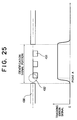
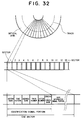
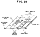
- Fig. 39 is an enlarged perspective view of such a conventional optical disk.
- the reference numeral 201 designates a recording layer which is, for example, formed from a phase change material.
- the reference numeral 202 designates recording pits; and 203, a beam spot of laser light.
- the reference numeral 204 designates concave portions formed from guide grooves; and 205, convex portions between guide grooves. The width of each of the concave portions 204 is set to be larger than the width of each of the convex portions 205.
- the reference numeral 206 designates pre-pits which form identification signals expressing position information on the disk. In the drawing, a transparent disk substrate which transmits incident light is not shown.
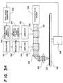
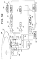
- Fig. 40 is a block diagram of the conventional optical information recording/reproducing apparatus.
- the reference numeral 207 designates an optical disk; and 208, a recording track which is constituted by a concave portion 204 in this case.
- the reference numeral 210 designates a semiconductor laser; 211, a collimator lens for collimating laser light emitted from the semiconductor laser 210; 212, a half mirror arranged on a light bundle; and 213, an objective lens for converging collimated light passing the half mirror 212 onto a recording surface of the optical disk 207.
- the reference numeral 214 designates a photo detector for receiving light passing through the objective lens 213 and the half mirror 212 and reflected from the optical disk 207.
- the photo detector 214 is divided into two parts in parallel with the track direction of the disk in order to obtain a tracking error signal. That is, the photo detector 214 is constituted by two light-receiving portions 214a and 214b.
- the reference numeral 215 designates an actuator for supporting the objective lens 213. These parts are mounted on a head base not shown to form an optical head 216.
- the reference numeral 217 designates a differential amplifier which receives detection signals outputted from the light-receiving portions 214a and 214b; and 218, a low pass filter (LPF) which receives a differential signal outputted from the differential amplifier 217.
- LPF low pass filter
- the reference numeral 219 designates a tracking control circuit which receives the output signal of the LPF 218 and a control signal L1 from a first system controller 232 and gives a tracking control signal to a driving circuit 220 and a traverse control circuit 226.
- the reference numeral 220 designates a driving circuit for giving a driving current to the actuator 215.
- the reference numeral 221 designates an addition amplifier which receives detection signals outputted from the light-receiving portions 214a and 214b and generates a summation signal; 222, a high pass filter (HPF) which receives the summation signal from the addition amplifier 221 and delivers high-frequency components of the summation signal to a waveform shaping circuit 223; 223, a first waveform shaping circuit which receives high-frequency components of the summation signal from the HPF 222 and delivers a digital signal to a reproduction signal processing circuit 224 and a first address reproducing circuit 225; and 224, a reproduction signal processing circuit which delivers an information signal such as an audio signal to an output terminal 233.
- HPF high pass filter
- the reference numeral 225 designates a first address reproducing circuit which receives the digital signal from the first waveform shaping circuit 223 and delivers an address signal to a first system controller 232.
- the reference numeral 226 designates a traverse control circuit which gives a driving current to a traverse motor 227 on the basis of a control signal L2 given from the first system controller 232; and 227, a traverse motor for moving the optical head 216 in the direction of the radius of the optical disk 207.
- the reference numeral 228 designates a spindle motor for rotating the optical disk 207.
- the reference numeral 229 designates a recording signal processing circuit which receives an information signal such as an audio signal from an external input terminal 230 and delivers a recording signal to a laser driving circuit 231; and 231, a laser driving circuit which receives a control signal L3 from the first system controller 232 and the recording signal from the recording signal processing circuit 230 and gives a driving current to the semiconductor laser 210.
- the reference numeral 232 designates a first system controller which delivers control signals L1 to L3 to the tracking control circuit 219, the traverse control circuit 226 and the recording signal processing circuit 229 and receives the address signal from the first address reproducing circuit 225.
- a laser beam radiated from the semiconductor laser 210 is collimated by the collimator lens 211 and converged onto the optical disk 207 by the objective lens 213 via the beam splitter 212.
- the light beam reflected from the optical disk 207 carries information of recording track 208 by diffraction and is led onto the photo detector 214 by the beam splitter 212 via the objective lens 213.
- the light-receiving portions 214a and 214b convert the changes of the light quantity distribution of the incident light beam into electric signals and deliver the electric signals to the differential amplifier 217 and the addition amplifier 221.
- the differential amplifier 217 subjects the respective input currents to I-V conversion, calculates difference between voltage values and delivers the difference signal as a push-pull signal.
- the LPF 218 extracts low-frequency components from the push-pull signal and delivers the low-frequency components as a tracking error signal to the tracking control circuit 219.
- the tracking control circuit 219 gives a tracking control signal to the driving circuit 220 in accordance with the level of the input tracking error signal, so that the driving circuit 220 supplies a driving current to the actuator 215 in accordance with the tracking control signal to thereby control the position of the objective lens 213 in the recording track-crossing direction.
- the beam spot performs scanning on the convex portion 205 correctly.
- the position of the objective lens 213 is controlled in the direction perpendicular to the disk surface by a focussing control circuit not shown in order to focus the beam spot onto the disk correctly.
- the addition amplifier 221 subjects the output currents of the light-receiving portions 214a and 214b to I-V conversion, adds voltage values and delivers the resulting signal as a summation signal to the HPF 222.
- the HPF 222 cuts off unnecessary low-frequency components from the summation signal, makes the reproducing signal as a main information signal and the address signal pass in analog waveform and delivers the signals to the first waveform shaping circuit 223.
- the first waveform shaping circuit 223 performs data slicing of the analog waveform main information signal and address signal by a predetermined threshold to form a pulse waveform and delivers the pulse waveform to the reproducing signal processing circuit 224 and the first address reproducing circuit 225.
- the reproduction signal processing circuit 224 decodes the input digital main information signal, applies processes such as error correction to the decoded signal and delivers the resulting signal as an audio signal or the like to the output terminal 233.
- the first address reproducing circuit 225 decodes the input digital address signal and delivers the decoded signal, as information of position on the disk, to the system controller 232. That is, as a result of scanning of the beam spot 203 on recording pits 202, a reproducing signal is given to the reproduction signal processing circuit 223, and as a result of scanning on pre-pits 206, an address signal is given to the first address reproducing circuit 225.
- the first system controller 232 judges on the basis of the address signal whether the light beam is currently fit to the desired address.
- the traverse control circuit 226 gives a driving current to the traverse motor 227 in accordance with the control signal L2 given from the first system controller 232 at the time of transferring of the optical head to thereby move the optical head 216 to the target track.
- the tracking control circuit 219 temporarily interrupts tracking servo on the basis of the control signal L1 given from the first system controller 232.
- the traverse motor 227 is driven in accordance with low-frequency components of the tracking error signal given from the tracking control circuit 219 to thereby move the optical head 216 slowly in the direction of the radius of the disk with the advance of reproduction.
- the recording signal processing circuit 229 adds an error code or the like to an audio signal or the like inputted from the external input terminal 230 at the time of recording and delivers the resulting signal as a coded recording signal to the laser driving circuit 231.
- the laser driving circuit 231 modulates a driving current to be applied to the semiconductor laser 210 in accordance with the recording signal.
- the intensity of the beam spot radiated onto the optical disk 207 changes according to the recording signal, so that recording pits 202 are formed.
- the laser driving circuit 231 is set to a reproducing mode through the control signal L3, so that a driving current is controlled to emit light from the semiconductor laser 210 at constant light intensity.
- a driving current is controlled to emit light from the semiconductor laser 210 at constant light intensity.
- the spindle motor 228 rotates the optical disk 207 at a constant angular velocity.
- the width of the convex portion 205 is narrowed so that the distance between tracks is reduced.
- the diffraction angle of reflected light due to the concave portion 203 becomes large. Accordingly, there arises a problem in that the tracking error signal for making the beam spot 203 follow a track with high accuracy is lowered.
- the width of the concave portion 204 must be narrowed. As a result, the size of the recording pits 202 is reduced, so that there arises a problem in that the amplitude of the reproducing signal is lowered.
- Fig. 41 is an enlarged perspective view of such an optical disk.
- the reference numeral 201 designates a recording layer; 202, recording pits; and 203, a beam spot of laser light.
- the reference numeral 240 designates concave portions formed as guide grooves; and 241, convex portions between guide grooves. As shown in the drawing, the width of each of the concave portions 240 is set to be substantially equal to the width of each of the convex portions 241.
- the reference numeral 242 designates pre-pits which are formed both in the concave portions 240 and in the convex portions 241 and placed in the respective heads of sectors in the two types of recording tracks so as to serve as identification signals expressing information of position on the optical disk.
- the recording pits 202 are formed both in the concave portions 240 and in the convex portions 241 as shown in the drawing.
- the guide groove pitch of the operational disk in Fig. 41 is equal to that of the optical disk in Fig. 39, but the distance between recording pit trains is reduced to 1/2. As a result, the recording capacity of the optical disk is increased to two times.
- the concave portions 240 and the convex portions 241 in this type optical disk are generically called "recording tracks" in the meaning that recording pits 202 are formed.
- the recording/reproducing operation of the optical information recording/reproducing apparatus for recording information signals in this type optical disk is carried out substantially in the same manner as the conventional optical information recording/reproducing apparatus shown in Fig. 40.
- This can be realized by inserting an on/off controllable inversion amplifier in between the LPF 218 and the tracking control circuit 219 in Fig. 40.
- identification signals such as pre-pits must be formed in the two types of recording tracks in order to obtain positional information in arbitrary position on the concave and convex recording tracks.
- the manufacturing process is complicated compared with the conventional optical disk shown in Fig. 39.
- An object of the present invention is to solve the above-mentioned problems, that is, to provide an optical information recording medium in which positional information can be obtained in two types recording tracks without formation of identification signals such as an address signal, etc. both in concave recording tracks and in convex recording tracks.
- the above object is achieved by an optical information recording medium according to claim 1 and by an optical information recording/reproducing apparatus according to claim 9, respectively.
- the invention starts from the teaching that is to be taken from JP-A-2177027.
- US-A-4949331 discloses preformed header signal pits in the land portions of a pregrooved optical medium.
- a phase change type recording material in which recording is performed on the basis of the change of real reflectance is used as a recordable/reproducible optical disk, and a constant angular velocity (hereinafter referred to as "CAV") control system is used as an optical disk rotating control system.
- CAV constant angular velocity
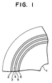
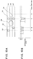
- Fig. 1 is a plan view of a first optical disk.
- the reference numeral 1 designates a first optical disk; 2, 4 and 6, concave recording tracks (hereinafter referred to as “concave portions”) constituted by guide grooves; and 3 and 5, convex recording tracks (hereinafter referred to as “convex portions”) constituted by regions between guide grooves.
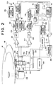
- Fig. 2 is a block diagram of a first optical information recording/reproducing apparatus.
- the reference numeral 40 designates a first optical disk using concave portions and convex portions as recording tracks; and 41, a recording track.
- an identification signal is preliminarily formed only in the concave portions.
- the reference numeral 210 designates a semiconductor laser; 211, a collimator lens; 212, a half mirror; 213, an objective lens; 214, a photo detector; 214a and 214b, light-receiving portions thereof; 215, an actuator; 216, an optical head; 217, a differential amplifier; 218, a low pass filter (LPF); 219, a tracking control circuit; 220, a driving circuit; 221, an addition amplifier; 222, a high pass filter (HPF); 223, a first waveform shaping circuit; 224, a reproduction signal processing circuit; 226, a traverse control circuit; 227, a traverse motor; 228, a spindle motor; 229, a recording signal processing circuit; 230, an external input terminal; 231, an LD driving circuit; and 233, an output terminal.
- These parts are substantially similar to constituent parts of a conventional optical recording/reproducing apparatus shown in Fig. 40. Accordingly, reference numerals given to the constituent parts of the conventional apparatus are given
- the reference numeral 50 designates a first polarity inverting circuit which receives a control signal L4 from a first system controller 56 and transmits a tracking error signal outputted from the LPF 218 to the tracking control circuit 219. With respect to the polarity for tracking control, it is assumed that tracking leading-in is performed on concave recording tracks in the case where a tracking error signal is inputted to the tracking control circuit 219 directly from the differential amplifier without any change of the polarity.
- the reference numeral 51 designates a second waveform shaping circuit which receives high-frequency components of a summation signal from the HPF 222 and gives a digital signal to the other input terminal of a first selector 52.
- the reference numeral 52 designates a first selector which receives a control signal L5 from a second system controller 56 and transmits outputs of the first and second waveform shaping circuits 223 and 51 to a second address reproducing circuit 53.
- the reference numeral 53 designates a second address reproducing circuit which receives the digital signal from the first selector 52 and gives address data to a second system controller 56.
- the reference numeral 54 designates a jump pulse generating circuit which receives a control signal L6 from the second system controller 56 and gives a jump pulse signal to one input terminal of a second selector 55.
- the reference numeral 55 designates a second selector which receives a switching signal L7 from the second system controller 56 and transmits the jump pulse signal from the jump pulse generating circuit 54 and the tracking control signal from the tracking control circuit 219 to the driving circuit 220.
- the reference numeral 56 designates a second system controller which receives an address signal from the second address reproducing circuit 53 and gives control signals L1 to L7 to the tracking control circuit 219, the traverse control circuit 226, the LD driving circuit 231, the recording signal processing circuit 229, the polarity inverting circuit 50, the first selector 52, the jump pulse generating circuit 54 and the second selector 55 respectively.
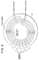
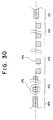
- Fig. 3 is a plan view showing the structure of recording tracks.
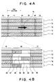
- Figs. 4A to 4C are structural views of a sector format.
- the reference numeral 61 designates concave portions; and 62, convex portions.
- Recording track numbers are assigned to respective tracks so that the tracks are numbered through the concave and convex portions at intervals of one rotation.
- a beam spot rotates to perform tracing clockwise from the inner circumferential side to the outer circumferential side so that recording track numbers are represented by T, T+1, T+2, T+3 and T+4 in the drawing.
- One rotation of each track is divided into N sectors so that sector numbers of from No. 1 to No. N are assigned to the N sectors. Because the recording tracks are shaped like a helical coil, the concave portions are formed so that sector No. N of track No. T is connected to sector No. 1 of track No. T+2.
- the convex portions are formed so that sector No. N of track No. T+1 is connected to sector No. 1 of track No. T+3.
- These recording track numbers and sector numbers are preliminarily formed on the disk as pre-pits as described above. Because the optical disk in this embodiment uses a CAV system as described above, boundaries between sectors are arranged on lines radially.
- Fig. 4A is a structural view of a sector format of the first optical disk 40.
- the transverse direction represents a track direction
- the longitudinal direction represents a disk radius direction.
- the reference numeral 70 designates a beam spot tracing direction.
- the reference numerals 71, 73 and 75 designate concave portions; and 72 and 74, convex portions.
- the reference numerals 76, 77, 78 and 79 designate main information signal portions for recording digitalized information signals such as audio signals, video signals, etc.; and 80, 81 and 82, identification signal portions provided on concave portions. Areas 89 and 90 which are provided on convex recording tracks so as to be radially adjacent to these identification signal portions are provided as blank areas where nothing is recorded.
- Identification signal portions are disposed before the main information signal portions respectively, so that a combination of one identification signal portion and one main information signal portion forms one sector.
- Fig. 4B shows an identification signal portion which is enlarged in the track direction.
- the reference numerals 83, 84 and 85 designate address areas in which pre-pits or the like are formed in respective sectors.
- the address areas 83, 84 and 85 are formed only on concave portions as described above. Because data stored in each of the address areas contains information such as track number and sector number and because the address areas are formed only on concave portions, track numbers in the address areas are picked up alternately so as to be represented by T, T+2, T+4... Sector numbers can be defined so that the same value is given to radially adjacent sectors.
- the reference numerals 86, 87 and 88 designate blank areas which are disposed before or after the address areas so as to be adjacent to the address areas and in which no signal is recorded.
- the length of each of the blank areas 86, 87 and 88 is equal to the length of each of the address areas 83, 84 and 85.
- the address areas 83, 84 and 85 and the blank areas 86, 87 and 88 are arranged alternately correspondingly to the concave portions.
- Fig. 4C is a structural view of the inside of each address area.
- One address area is composed of a sector mark block, a sync pattern block, an address mark block, a track number block, and a sector number block.
- the respective blocks function as follows.
- the sector mark block, the sync pattern block and the address mark block may be equalized in all sectors.
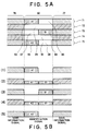
- Fig. 5A is a detailed structural view of an identification signal portion similar to Fig. 4B. Like numerals in each of Figs. 5A and 4B refer like parts.
- Fig. 5B is a timing chart of a reproducing signal in the case where a beam spot traces convex and concave portions. In Fig.
- the diagram (1) is a timing chart in the case where the concave portion 71 is traced
- the diagram (2) is a timing chart in the case where the convex portion 72 is traced
- the diagram (3) is a timing chart in the case where the concave portion 73 is traced
- the diagram (4) is a timing chart in the case where the convex portion 74 is traced
- the diagram (5) is a timing chart in the case where the concave portion 75 is traced.
- the transversal axis represents time
- the longitudinal axis represents the amplitude of the reproducing signal.
- the broken lines between Figs. 5A and 5B show correspondence between position and time.
- data (track number and sector number) in the address portions 83, 84 and 85 are replaced by A1, B1 and A2, respectively.
- a beam spot performs tracing on the address areas 83 and 85 arranged in the first half of the identification signal portion to thereby reproduce addresses A1 and A2 as shown in the diagrams (1) and (5).
- a beam spot performs tracing on the address area 84 arranged in the second half of the identification signal portion to thereby reproduce an address B1 as shown in the diagram (3).
- a signal component obtained from the quantity of reflection light modified with a pre-pit of an address area by scanning of the center of the beam spot 70 just above the address area as described above is hereinafter referred to as "main component".
- the convex portion 72 there is no main component reproduced from the blank area 89 of the identification signal portion even if the beam spot traces the blank area 89, but address signals A1 and B1 based on pre-pits of the address areas 83 and 84 of the adjacent concave portions 71 and 73 are reproduced as crosstalk as shown in the diagram (2).
- these components are referred to as "crosstalk components”. Because the address areas of the adjacent concave portions are arranged alternately, the crosstalk component from the address area 83 and the crosstalk component from the address area 84 are reproduced while separated with respect to time.
- the amplitude of these crosstalk signals is made smaller than the amplitude of signals reproduced in the case where the beam spot traces the address areas 83 and 85. Further, because there is no main information signal recorded in the blank area 89, unnecessary signal components except the crosstalk signals from the address areas 83 and 84 are prevented from mixing as noise.
- the case of the convex portion 74 is similar to the case of the convex portion 72, so that address values B1 and A2 of the address areas 84 and 85 are reproduced as crosstalk. Accordingly, track numbers of concave portions adjacent to the convex portion can be known by detecting these crosstalk signals, so that the track number of the currently traced convex portion can be calculated.
- the sector number of the convex portion can be known directly from the sector numbers of concave portions adjacent to the convex portion.
- the track numbers of the tracks 71, 72, 73, 74 and 75 in Fig. 5A are T, T+1, T+2, T+3 and T+4 respectively
- the track numbers recorded as pre-pits in the address areas 83, 84 and 85 are T, T+2 and T+4 respectively.
- the operation of the optical information recording/reproducing apparatus configured as described above will be described. Because the processes of radiation of a laser beam to the first optical disk 40 and reflection of the laser beam therefrom are carried out in the same manner as in the conventional apparatus, the detailed description of this apparatus will be omitted but only the point where this apparatus is different from the conventional apparatus, that is, how to perform the operation of detecting identification signals from pre-pits or the like and retrieving information (hereinafter referred to as "seek operation"), will be described below.
- the second system controller 56 judges by reference to an address map or the like whether the sector of the designated address exists in a convex portion or whether the sector exists in a concave portion.
- the sector of the designated address exists in a convex portion, the polarity of an input signal to the first polarity inverting circuit 50 is inverted through the control signal L4 so that the polarity-inverted signal is outputted from the first polarity inverting circuit 50.
- the sector of the designated address exists in a convex portion, the polarity of a signal is not changed so that the signal is outputted directly.
- the second system controller 56 gives the control signal L5 to the first selector 52 and makes the first selector 52 select either of the output of the first waveform shaping circuit 223 and the output of the second waveform shaping circuit 51 so that the former output is used as an input source to be given to the second address reproducing circuit 53 when the sector of the designated address exists in a concave portion, and the latter output is used as the input source when the sector of the designated address exists in a convex portion.
- the second selector 55 is made to select the tracking control circuit 219 through the control signal L7 so that the output of the tracking control circuit 219 is to be supplied to the driving circuit 220.
- the traverse control circuit 226 is made to drive the traverse motor 227 through the control signal L2 to thereby move the optical head 216 near to a track in which the target address exists.
- This operation is called "rough seek".
- this movement is carried out on the basis of comparison between the number of tracks preliminarily calculated from difference between the address value before the movement and the target address value and the number of traverse tracks obtained from the tracking error signal during the movement.
- the tracking control circuit 219 is made to turn on through the control signal L1 to thereby control the beam spot to perform tracing on the convex or concave portion.
- the output currents of the light-receiving portions 214a and 214b are subjected to I-V conversion and addition amplification by the addition amplifier 221 in the same manner as shown in the description of the prior art with reference to Fig. 40. Then, after unnecessary frequency band components are removed by the HPF 222, the output of the HPF 222 is inputted to the first and second waveform shaping circuits 223 and 51.
- the first waveform shaping circuit 223 performs waveform shaping of an address signal from the reproduced main component to a digital signal whereafter the first selector 52 is made to deliver the digital signal to the second address reproducing circuit 53 through the control signal L5 given by the second system controller 56.
- the second address reproducing circuit 53 decodes address data from the digital and delivers the address data to the second system controller 56. Thereafter, the second system controller 56 performs control while regarding the address data as a current address value.
- the second waveform shaping circuit 51 performs waveform shaping of an address signal from the reproduced crosstalk component to a digital signal whereafter the first selector 52 is made to deliver the digital signal to the second address reproducing circuit 53 through the control signal L5 given by the second system controller 56. Because the second waveform shaping circuit 51 performs waveform shaping after the input reproducing signal is amplified by a predetermined gain, even the waveform of a signal having small-amplitude crosstalk components can be shaped suitably.
- the second address reproducing circuit 53 decodes address data from the output of the first selector 52 and delivers the address data to the second system controller 56.
- the second system controller 56 calculates a current address value from the address data and thereafter performs control on the basis of the current address value. That is, as described above, the second system controller 56 receives two address values (A1 and B1 in the diagram (2) in Fig. 5B or B1 and A2 in the diagram (4) in Fig. 5B) from the second address reproducing circuit 53, calculates the number of a track between tracks designated by the two address values on the basis of the two address values and determines a current address value as well as a sector number common to the two.
- the second system controller 56 compares the current address value with the target address value. When the difference between the current address value and the target address value is not smaller than one track, the second system controller 56 makes the second selector 55 connect the output of the jump pulse generating circuit 54 to the input of the driving circuit 220 through the control signal L7 again. Then, the second system controller 56 gives the number of tracks to be jumped to the jump pulse generating circuit 54 through the control signal L6, so that the jump pulse generating circuit 54 supplies driving pulses to the driving circuit 220 to move the actuator 215 by a fine quantity to thereby perform jumping of the set number of tracks. This is called "fine seek". When the fine seek is completed so that the beam spot reaches the target track, tracking leading-in is performed so that the current address value is detected again. After the beam spot reaches the target sector by the rotation of the disk, an information signal is recorded on or reproduced from the target sector and sectors after the target sector in the same manner as shown in the description of the prior art in Fig. 40.
- the second system controller 56 controls the recording operation timing of the recording signal processing circuit 229 and the LD driving circuit 231 through the control signal L3 to prevent recording of main information signals or the like on the blank areas 86, 87, 88, 89 and 90 shown in Fig. 4B.
- the address areas 83 and 84 arranged on the concave recording tracks 71 and 73 are shifted so as not to be adjacent to each other in the track-crossing direction. Accordingly, in the case where the beam spot 70 traces the convex recording track 72, crosstalk components of two identification signals in a detection signal outputted from the photo detector 214 are provided by means of time division. Accordingly, the second wave-form shaping circuit 51 can perform two-valuing of the identification signal from the crosstalk component suitably, so that the second address reproducing circuit 53 can decode address information accurately.
- address information can be obtained in two types recording tracks, that is, concave and convex recording tracks, it is possible to form address areas only in the concave recording tracks in order to reduce the number of processes for producing an optical disk. Furthermore, because main information signals or the like are not recorded in the blank areas 86, 87, 88, 89 and 90 at the time of recording, unnecessary recording signals are prevented from mixing as noise in the crosstalk component of the reproduced identification signal. Accordingly, accuracy in reading address information can be improved.
- this embodiment shows a seeking operation in which the second system controller 56 selects the polarity of the output of the first polarity inverting circuit 50 at the time of starting of seeking on the basis of judgment as to whether the destination of seeking is a concave recording track or a convex recording track to thereby move the beam spot to the target recording track through rough seeking and fine seeking
- a seeking operation from a concave portion to a concave portion or from a convex portion to a convex portion and a seeking operation from a concave portion to a convex portion or from a convex portion to a concave portion are switched over as follows.
- the beam spot can be made to reach the target recording track directly if the second system controller 56 performs rough seeking and fine seeking without changing the polarity of the output of the first polarity inverting circuit 50.
- the second system controller 56 performs rough seeking and fine seeking without changing the polarity of the output of the first polarity inverting circuit 50 to thereby make the beam spot reach a recording track adjacent to the target recording track. Then, the polarity of the output of the first polarity inverting circuit 50 is inverted and, at the same time, a driving pulse signal corresponding to track jumping of the beam spot by the width of 1/2 of the guide groove pitch is generated from the jump pulse generating circuit 54 to the driving circuit 220.
- Such 1/2 track jumping can be substantially realized by using the 1 track jumping method employed in the conventional optical disk. That is, such 1/2 track jumping can be substantially realized by the same method as Bang-Bang control using acceleration/deceleration pulses at regular intervals as disclosed in Murayama et al., "Optical Disk Technique (Third Edition)", pp. 163-164, issued by RADIO GIJUTSUSHA. Because the polarity of a tracking error signal does not change at the time of starting of seeking if the seeking operation is carried out as described above, the number of traverse tracks at the time of rough seeking can be measured accurately so that a higher-speed seeking operation can be provided.
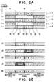
- FIG. 6A is a detailed structural view showing the vicinity of an identification signal portion of such a second optical disk.
- the reference numerals 71, 73 and 75 designate concave portions; 72 and 74, convex portions; 76 and 77, main information signal portions; 80, an identification signal portion; 89 and 90, blank areas; and 83, 84 and 85, address areas.
- the reference numerals 91, 92 and 93 designate address areas constituted by pre-pits.
- the pit pattern of each of the address areas 91, 92 and 93 is the same as the pit pattern of an adjacent address area on the disk inner circumferential side (the upper side in the drawing). That is, address signals A1 and B1 are recorded in the address areas 92 and 93, respectively. Though not shown in Fig. 5A, an address signal B0 is recorded in the address area 91.
- Fig. 6B is a timing chart of a reproducing signal in the case where the beam spot traces convex and concave portions.
- the diagram (1) is a timing chart in the case where the concave portion 71 is traced
- the diagram (2) is a timing chart in the case where the convex portion 72 is traced
- the diagram (3) is a timing chart in the case where the concave portion 73 is traced
- the diagram (4) is a timing chart in the case where the convex portion 74 is traced
- the diagram (5) is a timing chart in the case where the concave portion 75 is traced.
- the transversal axis represents time
- the longitudinal axis represents the amplitude of the reproducing signal.
- a beam spot performs tracing on the address areas 83 and 91 to thereby reproduce addresses A1 and A2 as shown in the diagram (1).
- a beam spot performs tracing on the address areas 92 and 84 to thereby reproduce addresses A1 and B1 as shown in the diagram (3).
- a beam spot performs tracing on the address areas 85 and 93 to thereby reproduce addresses A2 and B1 as shown in the diagram (5).
- main components modulated with pre-pits of address areas are obtained as address signals.
- bit patterns of the two adjacent address areas 91 and 84 are different from each other (B0 and B1), so that the reproducing signal synthesized from crosstalk components obtained from the two adjacent address areas 91 and 84 respectively is made error.
- This signal is not used as an address signal.
- the address value B1 of adjacent address areas 84 and 90 is reproduced as an address signal. Accordingly, the track numbers of two adjacent concave portions can be known by detecting these address signals, so that the track number of the currently traced convex portion can be calculated. Assuming now that the track numbers of the tracks 71, 72, 73, 74 and 75 in Fig.
- the track numbers of the pit patterns B0, A1, B1 and A2 are set to T-1, T+1, T+3 and T+5 respectively.
- the track numbers of the address signals to be reproduced are T+1 and T-1 in the first and second halves respectively. Accordingly, by averaging the two numbers according to the arithmetic operation ⁇ (T+1)+(T-1) ⁇ /2, the correct track number T can be obtained.
- the track numbers of the address signals to be reproduced are T+1 and error in the first and second halves respectively.
- T+1 is employed as the track number directly.
- Fig. 7 is a block diagram of the optical information recording/reproducing apparatus.
- the reference numeral 210 designates a semiconductor laser; 211, a collimator lens; 212, a half mirror; 213, an objective lens; 214, a photo detector; 214a and 214b, light-receiving portions thereof; 215, an actuator; 216, an optical head; 217, a differential amplifier; 218, a low pass filter (LPF); 219, a tracking control circuit; 220, a driving circuit; 221, an addition amplifier; 222, a high pass filter (HPF); 224, a reproduction signal processing circuit; 226, a traverse control circuit; 227, a traverse motor; 228, a spindle motor; 229, a recording signal processing circuit; 230, an external input terminal; 231, an LD driving circuit; 233, an output terminal; 50, a first polarity inverting circuit; 223, a first waveform
- the reference numeral 100 designates a second optical disk using Gray code as track number in the identification signal portion.
- the reference numeral 101 designates a recording track of the second optical disk 100.
- the reference numeral 102 designates a fourth waveform shaping circuit which receives an output signal from the HPF 222 and gives a digital signal to a Gray code decoding circuit.
- the reference numeral 103 designates a Gray code decoding circuit which receives the digital signal from the fourth waveform shaping circuit 102 and a control signal L8 from a third system controller and gives address data to the third system controller.
- the reference numeral 104 designates a fifth waveform shaping circuit which receives an output signal from the HPF 222 and gives a digital signal to an addition Gray code decoding circuit.
- the reference numeral 105 designates an addition Gray code decoding circuit which receives the digital signal from the fifth waveform shaping circuit 104 and a control signal L8 from the third system controller and gives address data to the third system controller.
- the reference numeral 106 designates a third system controller which receives address signals from the Gray code decoding circuit 103 and the addition Gray code decoding circuit 105 and gives control signals L1, L2, L3, L4, L6, L7 and L8 to the tracking control circuit 219, the traverse control circuit 226, the LD driving circuit 231, the first polarity inverting circuit 50, the jump pulse generating circuit 54, the second selector 55, the Gray code decoding circuit 103 and the addition Gray code decoding circuit 105 respectively.
- this embodiment is characterized in that so-called Gray code patterns are used as identification signals arranged on the second optical disk 100.
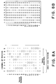
- Figs. 8A and 8B show an example of Gray code patterns adapted to track numbers.
- 16 kinds of 9-bit unit patterns from 1 to 16 are set as Gray code patterns and assigned for track numbers so that a series of patterns is repeated every 16 tracks.
- Fig. 8A shows a series of patterns on the disk.
- "o" represents the existence of pits
- "-" represents the non-existence of pits
- the transversal numerals represent channel bit positions
- the longitudinal numerals represent track numbers.
- Fig. 8B shows binary codes obtained by reading the Gray code patterns in Fig. 8A.
- this series of patterns is characterized in that the bit position in one of unit patterns of adjacent tracks always changes by one channel bit compared with the bit pattern in the other unit pattern of the adjacent tracks.
- Figs. 9A and 9B are structural views of a sector in the second optical disk 100 in this embodiment.
- the reference numeral 70 designates the direction of tracing of the beam spot.
- the reference numerals 111, 113 and 115 designate concave portions; 112 and 114, convex portions; 116, 117, 118 and 119, main information signal portions; 120, 121 and 122, identification signal portions; and 126 and 127, blank areas. Because this structure is equivalent to the sector structure in the first embodiment shown in Figs. 4A to 4C, the detailed description thereof will be omitted.
- the reference numerals 128, 129 and 130 designate address areas formed on the concave portions 111, 113 and 115 and having the same structure as shown in Fig. 4C. Track numbers and sector numbers are expressed by Gray code patterns shown in Figs. 8A and 8B.
- the beam spot performs tracing on the address areas 128, 129 and 130 directly so that information, such as sector mark, sync pattern, address mark, track number and sector number, recorded in these areas can be reproduced.
- the Gray codes of track number and sector number thus reproduced are converted into generally-used binary codes through a conversion table using memory or the like.
- the beam spot performs tracing on the blank areas 126 and 127 but signals recorded in address areas on the opposite sides of the blank areas are reproduced as crosstalk in the same manner as described above in the first embodiment.
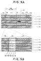
- Figs. 10A and 10B are views showing the relation between pit arrangement on concave portions and reproducing signal waveform in the case where the beam spot traces a convex portion.
- Fig. 10A is a view of arrangement of pits
- Fig. 10B is a graph view of reproducing signal waveform.
- the reference numerals 131, 132, 133 and 134 designate pre-pits set as identification signals on concave portions in advance.
- the reference numerals 135 and 137 designate concave portions; and 136, a convex portion.
- Fig. 10A the reference numerals 131, 132, 133 and 134 designate pre-pits set as identification signals on concave portions in advance.
- the reference numerals 135 and 137 designate concave portions; and 136, a convex portion.
- Fig. 10A the reference numerals 131, 132, 133 and 134 designate pre-pits set as identification signals on concave portions
- the abscissa represents the tracking-direction position of the beam spot, and the ordinate represents the quantity of reproduced light. Because the optical information recording/reproducing apparatus in this embodiment uses CAV control, pre-pits in address areas are aligned in radial directions. Accordingly, when attention is given to one convex track, pit arrangement of concave portions on opposite sides of the convex portion is classified into the following three cases: the case where a pit exists in either of the concave portions on opposite sides of the convex portion as represented by position A and position B in Fig. 10B; the case where pits exist in the opposite sides as represented by position C in Fig. 10B; and the case where there is no pit on the opposite sides as represented by position D in Fig. 10B.
- the quantity of reproduced light is as shown in Fig. 10B.
- the quantity of reproduced light in positions A and B is reduced by ⁇ as shown in Fig. 10B because of scattering of the beam caused by the pit of the adjacent concave portion whereas the quantity of reproduced light in position C is reduced by ⁇ larger than ⁇ because of scattering of the beam caused by the pits of the two adjacent concave portions.
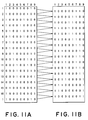
- Fig. 11A shows Gray codes arranged in concave recording tracks
- Fig. 11B shows two-valued codes of crosstalk summation signals in convex recording tracks.
- the Gray codes shown in Fig. 11A are the same as the Gray codes shown in Fig. 8B.
- Fig. 11B shows results of summation of codes of adjacent track numbers shown in Fig. 11A.
- the results of summation are called "addition Gray codes”. Because Gray codes of adjacent tracks are formed so that any one bit position in the unit pattern changes by one channel bit, it is apparent from Fig. 11B that the summation Gray codes are different from each other.
- the respective track numbers of the concave portions on the opposite sides can be identified so that the track number of the convex portion can be identified.
- an address signal can be detected in accordance with the Gray code pattern.
- the third system controller 106 judges by reference to an address map or the like whether the sector of the designated address exists in a convex portion or whether the sector exists in a concave portion.
- the sector of the designated address exists in a convex portion, the polarity of an input signal to the first polarity inverting circuit 50 is inverted through the control signal L4 so that the polarity-inverted signal is outputted from the first polarity inverting circuit 50.
- the sector of the designated address exists in a convex portion, the polarity of a signal is not changed so that the signal is outputted directly.
- the third system controller 106 gives the control signal L8 to the Gray code decoding circuit 103 and the addition Gray code decoding circuit 105 so that the Gray code deciding circuit 103 and the addition Gray code decoding circuit 105 are turned to an operative state and an inoperative state respectively when the given address is in a concave portion, and the Gray code deciding circuit 103 and the addition Gray code decoding circuit 105 are turned to an inoperative state and an operative state respectively when the given address is in a convex portion. In these states, rough seeking and tracking leading-in are performed.
- the reproducing signals from the light-receiving portions 214a and 214b are inputted to the first waveform shaping circuit 223, the fourth waveform shaping circuit 102 and the fifth waveform shaping circuit 104 via the addition amplifier 221 and the HPF 222.
- the fourth waveform shaping circuit 102 performs waveform shaping to a digital signal by two-valuing the reproducing signal reproduced from the address area of the concave portion and delivers the digital signal to the Gray code decoding circuit 103.
- the Gray code decoding circuit 103 converts track number expressed in Gray code into general address data allowed to be used in the system controller on the basis of a conversion table constituted by memory or the like and delivers the address data together with other identification signals such as sector number to the third system controller 106. Thereafter, the system controller 106 performs control while regarding the address data as a current address value.
- the fifth waveform shaping circuit 104 performs waveform shaping to a digital signal by two-valuing the reproducing signal reproduced by crosstalk from identification signal portions of two concave portions adjacent to the convex portion and delivers the digital signal to the addition Gray code decoding circuit 105.
- the addition Gray code decoding circuit 105 converts track number expressed in Gray code into general address data allowed to be used in the system controller on the basis of a conversion table constituted by memory or the like and delivers the address data together with other identification signals such as sector number to the third system controller 106. Thereafter, the third system controller 106 performs control while regarding the address data as a current address value.
- Gray codes are used as track numbers arranged as pre-pits in the address areas 128 and 129, so that when the beam spot traces a convex recording track 112, the addition Gray code decoding circuit 105 can decode address information accurately by using crosstalk components obtained from the address areas 128 and 129. Accordingly, because address information can be obtained in two types of recording tracks, that is, concave and convex recording tracks, it is possible to form address areas only in concave recording tracks so that the number of processes required for manufacturing optical disks can be reduced.
- any other code may be used as the address code for track number as long as patterns generated by logical summation of adjacent unit patterns are different from each other. Examples of Gray code allowed to be used in this embodiment are shown in Figs. 12A to 12D. Alternatively, patterns as described in detail in JP-A 3-168927 may be used.
- a third optical disk and an optical information recording/reproducing apparatus using the disk will be described below in detail.
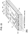
- Fig. 13 is an enlarged perspective view of a recording surface of a third optical disk according to the present invention.
- the reference numeral 301 designates a disk substrate; 302, a recording layer; 303, 304, 305 and 306, concave portions formed spirally and serving as guide grooves for tracking control; 307, 308 and 309, convex portions between the concave portions.
- the concave portions and the convex portions are arranged at intervals of the pitch Tp.
- the concave/convex portions are lined up in numerical order so that low-numbered concave/convex portions are arranged in the inner circumferential side.
- the reference numeral 310 designates pre-pits aligned in the convex-concave form in areas where guide grooves are interrupted.
- the respective center lines of pre-pit trains are shifted by 1/4 of Tp from the respective center lines of the guide grooves to the outer circumferential side. That is, one pre-pit area corresponds to a combination of a concave portion and a convex portion adjacent to each other.
- Identification signals are recorded according to the arrangement of such pre-pits 310.
- this drawing shows the case where the number of identification signal pre-pits is not larger than 3 per one track. The number of pre-pits is however actually from the order of tens to the order of hundreds according to the information capacity of the identification signal.
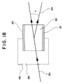
- the reference numeral 311 designates a beam spot converged into the recording layer by an objective lens and the like.
- the beam spot 311 is scanned along the center line of a concave or convex portion (hereinafter referred to as "track center") as shown in Fig. 13.
- the beam spot 311 moves on a concave or convex portion along the track center. Though the beam spot 311 reaches a guide groove interruption area, scanning is performed along the track center if the interruption area passing time is sufficiently short.
- the positional relation between the beam spot 311 and a pre-pit 310 in this case is shown in Fig. 14.
- Fig. 14 is an enlarged view of a recording surface of the optical disk in this embodiment, from just above.
- the beam spot 310 moves along the track center of a convex portion, the left half of the beam spot 310 overlaps a pre-pit 310.
- the reflected light of the beam spot is modulated with such a pre-pit. Accordingly, address information or the like can be obtained if the modulated light is detected by a photo detector or the like.
- the depth of the pre-pit 310 calculated as an optical length is set to 1/4 of the wave length of a radiation beam generating the beam spot, the degree of modulation of the reflected light can be maximized.
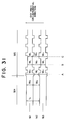
- Fig. 15 is a structural view of recording tracks.
- the reference numeral 320 designates concave portions; and 321, convex portions. Recording track numbers are assigned to respective tracks so that the tracks are numbered through the concave and convex portions at intervals of one rotation.
- a beam spot rotates to perform tracing clockwise from the inner circumferential side to the outer circumferential side so that recording track numbers are represented by T, T+1, T+2, T+3 and T+4 in the drawing.
- the reference numeral 322 designates sectors obtained by diving one rotation of each track into N groups. Sector numbers of from No. 1 to No. N are given to the N sectors, respectively.
- the concave portions are formed so that sector No. N of track No. T is connected to sector No. 1 of track No. T+2. Further, the convex portions are formed so that sector No. N of track No. T+1 is connected to sector No. 1 of track No. T+3.
- These recording track numbers and sector numbers are preliminarily formed on the disk as pre-pits as described above.
- address data in convex recording tracks are recorded as pre-pits.
- the current position information can ba obtained easily by adding 1 to the track number in the address data reproduced from pre-pits.
- the sector numbers of adjacent sectors in radial directions are equal to each other, signals reproduced from pre-pits in concave and convex recording tracks can be used as position information directly.
- Fig. 16 is a view for explaining the format of identification signals per one sector.
- one sector is composed of an identification signal area and a main information signal area.
- the identification signal area is composed of a sector mark block, a sync pattern block, an address mark block, a track number block, and a sector number block.
- the respective blocks function as follows.
- the sector mark block, the sync pattern block and the address mark block may be equalized in all sectors.
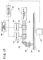
- Fig. 17 is a block diagram showing the configuration of the apparatus.
- the reference numeral 330 designates a radiation beam source such as a laser light source for radiating a radiation beam 331 having sufficient energy.
- the radiation beam 331 passes through a light intensity modulator 332, a light deflector 333 and a mirror prism 334 and is converged to a fine radiation beam spot by an objective lens 335.
- a radiation beam sensing layer 337 such as a photoresist layer is applied to a recording carrier 336 such as an optical disk substrate.
- the light intensity modulator 332 intercepts the radiation beam 331 in accordance with the identification signal given from an identification signal generator 338 through an amplifier 339. Accordingly, the identification signal outputted from the identification signal generator 338 is converted into radiation beam pulses and converted into photo-sensitive mark trains on the radiation beam sensing layer 337. Upon reception of gate pulse signal from a gate signal generator 340, the identification signal generator 338 generates an identification signal.
- the light intensity modulator 332 can be constituted by a photoelectric crystal for rotating the direction of deflection of the radiation beam in response to application of a voltage, and an analyzer for converting the direction change of a deflection surface into the change of light intensity.
- the light deflector 333 makes the angle of the radiation beam 331 change by a very small value so that the fine beam spot is moved by a predetermined width on the recording carrier in the direction of the radius thereof only when a gate pulse signal is given from the gate signal generator 340 connected through an amplifier 341.
- the gate signal generator 340 generates a gate pulse signal having a length equal to the length of the identification signal in a predetermined period in synchronism with a rotation phase signal outputted from a motor 342 for rotating the recording carrier 336 and delivers the gate pulse signal to the identification signal generator 338 and the amplifier 341.
- a continuous track is written on the radiation beam sensing layer when the gate pulse signal is absent, but an identification signal is written as a mark train in a position shifted by a predetermined quantity in the radial direction compared with the continuous track when the gate pulse signal is generated.
- the continuous track and the pre-pit train as an identification signal can be written on the radiation beam sensing layer 337 by a series of operations. That is, the identification signal is expressed by intermission of the continuous track.
- the light deflector 341 can be constituted by a so-called acoustic-optical deflector.
- Fig. 18 shows an acoustic-optical element used as the deflector 341.
- an acoustic-optical cell 350 is provided with two electro-mechanical transducers 351 and 352 connected to terminals 355 and 356 respectively.
- an electric signal is supplied between the terminals 355 and 356, an acoustic wave with a certain frequency is generated in a medium such as glass within the cell 350.
- Bragg refraction occurs in the medium so that a part of the radiation beam 353 is deflected by an angle ⁇ as a sub-beam 354.
- the angle ⁇ is proportional to the frequency of the supplied electric signal.
- the respective center lines of pre-pit trains are shifted by 1/4 of the guide groove pitch from the respective center lines of the guide grooves to the outer circumferential side. Accordingly, both in concave recording tracks and in convex recording tracks, the beam spot can be sufficiently modulated with pre-pits so that the identification signal can be detected. Further, there is no necessity of forming prepits both in concave recording tracks and in convex recording tracks, so that the number of processes required for production of an optical disk can be reduced.
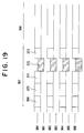
- FIG. 19 shows an example of a sector format of such a disk.
- the reference numerals 360, 362, 364 and 366 designate concave portions; 361, 363 and 365, convex portions; 367, an identification signal portion; 368, a main information signal portion; 369, an area in which a sector mark is recorded; 370, an area in which a sync pattern is recorded; 371, an area in which an address mark is recorded; 372, an area in which a track number is recorded; and 373, an area in which a sector number is recorded.
- this embodiment shows the case where an identification signal is arranged in a segment in which a concave portion constituted by a guide groove is interrupted
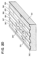
- the present invention can be applied to the case where identification signals are arranged by making pre-pits overlap a continuous guide groove as shown in Fig. 20. In this case, there is no interruption of the guide groove, so that tracking control is stabilized.
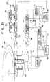
- Fig. 21 is a block diagram showing the configuration of the optical information recording/reproducing apparatus.
- the reference numeral 210 designates a semiconductor laser; 211, a collimator lens; 212, a half mirror; 213, an objective lens; 214, a photo detector; 214a and 214b, light-receiving portions thereof; 215, an actuator; 216, an optical head; 217, a differential amplifier; 218, a low pass filter (LPF); 219, a tracking control circuit; 220, a driving circuit; 221, an addition amplifier; 222, a high pass filter (HPF); 223, a first waveform shaping circuit; 224, a reproduction signal processing circuit; 225, an address reproducing circuit; 226, a traverse control circuit; 227, a traverse motor; 228, a spindle motor; 229, a recording signal processing circuit; 230, an external input terminal; 231, an laser driving circuit; and 233, an output terminal.
- the reference numeral 210 designates a semiconductor
- the reference numeral 50 designates a first polarity inverting circuit; 223, a first waveform shaping circuit; 54, a jump pulse generating circuit; and 55, a second selector. These parts are substantially similar to constituent parts of the first optical information recording/reproducing apparatus shown in Fig. 2.
- the reference numeral 400 designates a third optical disk as described above with reference to Fig. 13; 401, a recording track thereof; and 402, a sixth waveform shaping circuit which receives high-frequency components of a summation signal from the HPF 222 and delivers a digital signal to the address reproducing circuit 225.
- the reference numeral 403 designates an address calculation circuit which receives an address signal from the address reproducing circuit 225 and the control signal L4 from a fourth system controller and delivers a correct address signal to the fourth system controller.
- the reference numeral 404 designates a system controller which receives the address signal from the address calculation circuit 403 and delivers control signals L1, L2, L3, L4, L6 and L7 to the tracking control circuit 219, the traverse control circuit 226, the laser driving circuit 231, the recording signal processing circuit 229, the first polarity inverting circuit 50, the address calculation circuit 403, the jump pulse generating circuit 54 and the first selector 55 respectively.
- optical information recording/reproducing apparatus configured as described above will be described with reference to the drawings. Because the processes of radiation of a laser beam to the optical disk 400 and reflection of the laser beam therefrom are carried out in the same manner as in the conventional apparatus, the detailed description of this apparatus will be omitted but only the point where this apparatus is different from the conventional apparatus, that is, how to perform the operation of detecting identification signals from pre-pits or the like and seeking a target address, will be described below.
- the fourth system controller 404 judges by reference to an address map or the like whether the sector of the designated address exists in a convex portion or whether the sector exists in a concave portion, and outputs a judgment signal as L4. It is now assumed that the level of the signal L4 becomes low in the case of a concave portion whereas the level of the signal L4 becomes high in the case of a convex portion.
- the start address is an address in a convex portion
- the polarity of an input signal to the first polarity inverting circuit 50 is inverted.
- the start address is an address in a concave portion, the polarity of a signal is not changed so that the signal is outputted directly.
- the second selector 55 is made to select the tracking control circuit 219 through the control signal L7 so that the output of the tracking control circuit 219 is supplied to the driving circuit 220.
- the traverse control circuit 226 is made to drive the traverse motor 227 through the control signal L2 to thereby perform rough seeking. This movement is carried out on the basis of comparison between the number of tracks preliminarily calculated from difference between the address value before the movement and the target address value and the number of traverse tracks obtained from the tracking error signal during the movement.
- the tracking control circuit 219 is made to turn on through the control signal L1 to thereby control the beam spot to perform tracing on the convex or concave portion.
- the output currents of the light-receiving portions 214a and 214b are subjected to I-V conversion and addition amplification by the addition amplifier 221 in the same manner as shown in the description of the prior art with reference to Fig. 40. Then, after unnecessary frequency band components are removed by the HPF 222, the output of the HPF 222 is inputted to the first and sixth waveform shaping circuits 223 and 406. In the case where the beam spot performs tracing on an interruption area, the reproducing signal outputted from the HPF 222 is a signal modulated with pre-pits.
- the sixth waveform shaping circuit 402 Upon reception of the reproducing signal from the HPF 222, the sixth waveform shaping circuit 402 performs waveform shaping to a digital signal by amplifying the reproducing signal to predetermined amplitude and two-valuing the amplified reproducing signal, and delivers the digital signal to the address reproducing circuit 225.
- the address reproducing circuit 225 decodes address data from the digital signal and delivers the address data to the address calculation circuit 403.
- the address calculation circuit 403 delivers the input address data to the fourth system controller 404 directly while regarding the input address data as a current address.
- the address calculation circuit 403 adds 1 to the track number in the address data and delivers the resulting data to the fourth system controller 404. Thereafter, the fourth system controller 404 performs control while regarding the given value as a current address value.
- the fourth system controller 404 compares the current address value with the target address value. When the difference between the current address value and the target address value is not smaller than one track, the fourth system controller 404 makes the second selector 55 connect the output of the jump pulse generating circuit 54 to the input of the driving circuit 220 through the control signal L7 again. Then, the fourth system controller 404 gives the number of tracks to be jumped to the jump pulse generating circuit 54 through the control signal L6, so that the jump pulse generating circuit 54 supplies driving pulses to the driving circuit 220 to move the actuator 215 by a fine quantity to thereby perform jumping of the set number of tracks. When the beam spot reaches the target track, tracking leading-in is performed so that the current address value is detected again.
- the first waveform shaping circuit 223 After the beam spot reaches the target sector by the rotation of the disk, an information signal is recorded on or reproduced from the target sector and sectors after the target sector.
- the first waveform shaping circuit 223 upon reception of the reproducing from the HPF 222, the first waveform shaping circuit 223 performs waveform shaping to a digital signal by amplifying the reproducing signal to predetermined amplitude and two-valuing the amplified reproducing signal, and delivers the digital signal to the reproduction signal processing circuit 224. Because the amplitude of the main information signal based on recording marks is different from the reproduction amplitude of the identification signal based on pre-pits, the amplification factor of the first waveform shaping circuit 223 is set to be different from the amplification factor of the sixth waveform shaping circuit 402. The reproduction signal processing circuit 224 decodes the digital signal, corrects error and delivers the correct signal to the output terminal 233. Further, the operation of this apparatus at the time of recording is the same as that of the conventional optical information recording/reproducing apparatus shown in
- the fourth system controller 404 judges whether the track currently scanned by the light beam is a concave portion or a convex portion, so that the address calculation circuit 403 calculates the address of the position currently scanned by the light beam on the basis of the judgment result and the address data decoded by the address reproducing circuit 225. Accordingly, the address can be read correctly.
- this embodiment is adapted to an optical disk in which pre-pits are shifted by 1/4 of the guide groove pitch from the respective center lines of the guide grooves to the outer circumferential side
- the present invention can be also applied to an optical disk in which pre-pits are shifted to the inner circumferential side.
- the value to be added to the track number in the address calculation circuit 403 is changed from +1 to -1 when the level of the judgment signal L4 is high.
- Fig. 22 is a block diagram showing the configuration of the fourth optical information recording/reproducing apparatus.
- the reference numeral 50 designates a first polarity inverting circuit; 223, a first waveform shaping circuit; 402, a sixth waveform shaping circuit; 403, an address calculation circuit; 54, a jump pulse generating circuit; 55, a second selector; 404, a fourth system controller; 210, a semiconductor laser; 211, a collimator lens; 212, a half mirror; 213, an objective lens; 214, a photo detector; 214a and 214b, light-receiving portions thereof; 215, an actuator; 216, an optical head; 217, a differential amplifier; 218, a low pass filter (LPF); 219, a tracking control circuit; 220, a driving circuit; 221, an addition amplifier; 222, a high pass filter (HPF); 224, a reproduction signal processing circuit; 225, an address reproducing circuit; 226, a traverse control circuit; 227, a
- the reference numeral 410 designates a fourth optical disk; and 411, a recording track thereof.
- the reference numeral 412 designates a seventh waveform shaping circuit which receives an output from the HPF 222 and the control signal L4 from the fourth system controller 404 and delivers a signal to a sync signal detecting circuit; 413, a sync signal detecting circuit which receives the output signal of the seventh waveform shaping circuit 412 and delivers an address sync signal to a gate signal generating circuit; 414, a gate signal generating circuit which receives the address sync signal from the sync signal detecting circuit 413 and delivers first and second gate signals L8 and L9 to a hold circuit and a variable-gain amplifier respectively; 415, a hold circuit which receives the output of the first polarity inverting circuit 50 and the first gate signal of the gate signal generating circuit 414 and delivers a tracking error signal to the tracking control circuit 219; and 4
- Fig. 23 is an enlarged perspective view of the fourth optical disk 410.
- the reference numeral 420 designates a main information signal area constituted by concave and convex recording tracks formed from guide grooves; and 421, an identification signal area in which pre-pits are arranged so as to be shifted in the direction of the radius of the disk in the same manner as described above with reference to Fig. 13.
- the reference numeral 422 designates a sync signal area which is formed between the main information signal area 420 and the identification signal area 421 on extension lines of concave portions and in which pre-pits are formed by intermission of guide grooves. The pattern of the sync signal is common to all sectors.
- the reference numeral 301 designates a disk substrate; 302, a recording layer; 310, pre-pits; and 311, a beam spot.
- the first polarity inverting circuit 50 delivers the tracking error signal to the hold circuit 415 directly in accordance with the control signal L4 in the same manner as in the third optical information recording/reproducing apparatus shown in Fig. 21.
- the hold circuit 415 delivers the tracking error signal to the tracking control circuit 219 directly.
- the tracking control circuit 219 moves the actuator 215 through the driving circuit 220 to eliminate off-track in accordance with the tracking error signal.
- the second selector 55 connects the tracking control circuit 219 and the driving circuit 220 on the basis of the control signal L7.
- a sync signal recorded as arrangement of pre-pits 310 in the sync signal area 422 is inputted to the seventh waveform shaping circuit 412 through the photo detector 214, the addition amplifier 221 and the HPF 222.
- the seventh waveform shaping circuit 412 performs two-valuing of the reproduced sync signal on the basis of the first threshold Th1 and delivers the two-valued signal as a digital signal to the sync signal detecting circuit 413.
- the sync signal detecting circuit 413 always compares the pattern of the digital signal received from the seventh waveform shaping circuit 412 with the pattern of a sync signal preliminarily stored in the inside of the sync signal detecting circuit 412. When the two patterns coincide with each other, the sync signal detecting circuit 413 generates the first and second gate signals L8 and L9.
- Fig. 24 is a timing chart showing the first and second gate signals in the case where the beam spot passes through respective areas.
- the level of the first gate signal being generally low (Lo) turns to a high level (Hi) when the sync signal is detected, and then returns to a low level (Lo) when the time T1 required for the beam spot's passing through the identification signal area 421 passes away.
- the level of the second gate signal being generally low (Lo) turns to a high level (Hi) at a point of time of falling of the first gate signal from Hi to Lo and is kept high (Hi) till a predetermined time T2 passes away.
- a tracking error signal is inputted to the hold circuit 415 through the photo detector 214, the differential amplifier 217, the LPF 218 and the polarity inverting circuit 62.
- the hold circuit 415 When the level of the gate signal L8 is low, the hold circuit 415 outputs the input signal directly.
- the gate signal L8 rises from a low level (Lo) to a high level (Hi), the hold circuit 415 holds the value of the input signal just before the rising of the gate signal L8 and continuously outputs the value till the level of the signal L8 returns to a low level (Lo).
- the variable-gain amplifier 416 amplifies the input signal by gain A1 when the level of the gate signal L9 is low, and it amplifies the input signal by gain A2 when the level of the gate signal L9 is high.
- the gain is set to satisfy A1 ⁇ A2.
- Fig. 25 is a waveform view of a tracking error signal outputted from the polarity inverting circuit 50 in the case where the beam spot performs tracing on an identification signal area.
- the reference numeral 430 designates a concave portion; 431, pre-pits which are recorded so as to be shifted by Tp/4; and 432, a beam spot.
- the tracking error signal takes a large value as shown at point A in the waveform view.
- an excessive driving current is supplied to the actuator 215 rapidly, so that tracking control may be shaken so as to be unstable.
- the sync signal arranged just before the identification signal area is detected so that the hold circuit 415 holds the tracking error signal in accordance with the first gate signal L8 just before the beam spot starts tracing of the identification signal area. Accordingly, the tracking error signal is prevented from increasing rapidly in this area, so that tracking control is prevented from becoming unstable.
- the holding is released so that tracking control is restarted in accordance with the tracking error signal outputted from the first polarity inverting circuit 50.
- variable-gain amplifier 416 amplifies the tracking error signal by gain A2 to thereby increase the tracking control loop gain for time T2.
- the tracking control circuit 219 makes the actuator 215 generate a large driving force in the direction of elimination of tracking error through the driving circuit 220. Accordingly, tracking leading-in is performed rapidly so that off-track after releasing of the holding is eliminated soon.
- the time T2 is set to an optimum value under the consideration of the linear speed of the disk, the length of the time T1, the driving force of the actuator 215, etc.
- the first polarity inverting circuit 50 inverts the input tracking error signal on the basis of the control signal L4 given by the system controller. Accordingly, the beam spot traces a convex recording track.
- the second threshold Th2 different from the first threshold Th1 is set as a comparison level for two-valuing on the basis the control signal L4. The reason why the threshold is made variable between concave recording tracks and convex recording tracks will be described below with reference to the drawings.
- Fig. 26 is an enlarged view showing the positional relation between pre-pits in a sync signal area and a beam spot in the case where the beam spot traces a convex recording track.
- the reference numerals 440, 442, 444 and 446 designate concave portions; and 441, 443 and 445, convex portions.
- the reference numeral 447 designates a main information signal portion; 448, a sync signal area; 449, a beam spot; and 450, pre-pits.
- the patterns of sync signals are all equal, so that the patterns of arrangement of pits on opposite sides of the beam spot 449 coincide with each other.
- the beam spot 449 partly overlaps pre-pits in the concave portions 442 and 444 on the opposite sides so that the beam spot 449 is modulated with the pre-pits.
- the sync signal can be reproduced. Because the concave recording track is however different from the convex recording track in the area in which the beam spot overlaps pre-pits, the two types of tracks are also different in the degree of modulation of the reproduced sync signal.
- the thresholds Th1 and Th2 are set to optimum values in accordance with the degrees of modulation respectively, so that the sync signal can be two-valued well.
- the width Wp of the pre-pit 451 for sync signal may be set to be larger than the width Wg of the guide groove as shown in Fig. 27.
- the area in which the beam spot overlaps pre-pits at the time of tracing of a convex recording track is widened so that the degree of modulation of the reproducing signal is improved.
- Such pre-pits can be formed easily by increasing the intensity of the radiation beam to enlarge the photosensitive portion on the radiation beam sensing layer by using the optical disk producing apparatus as shown in Fig. 17.
- Fig. 28 is a view for explaining the structure of a recording track in which such a gap area is provided.
- a gap area having a length corresponding to the time T2 is provided just after the identification signal portion, so that recording of the main information signal is prevented unless the track offset is eliminated. In this manner, recording of the main information signal in an off-track state can be avoided, so that the quality of the recording signal can be improved.
- the sync signal arranged just before the identification signal area is detected, so that the hold circuit 415 holds the tracking error signal just before the beam spot starts tracing of the identification signal area.
- the driving current supplied to the actuator 215 is prevented from changing rapidly, so that tracking control can be stabilized.
- the variable-gain amplifier 416 keeps the tracking control loop gain in a large value for the time T2 just after releasing of the holding. In this manner, tracking leading-in is performed rapidly, so that off-track produced at the time of holding can be eliminated soon. Further, a gap portion having a length corresponding to the time T2 is provided. In this manner, recording of the main information signal in an off-track state can be avoided, so that the quality of the recording signal can be improved.
- Fig. 29 is a block diagram for detection of an identification signal in this case.
- the reference numeral 217 designates a differential amplifier; 218, an LPF; 50, a first polarity inverting circuit; 219, a tracking control circuit; 225, and an address reproducing circuit.
- the above configuration is the same as the configuration shown in Fig. 21.
- the reference numeral 460 designates a high pass filter (HPF) for extracting identification signal components from a push-pull signal outputted from the differential amplifier 217.
- HPF high pass filter
- the reference numeral 461 designates a second polarity inverting circuit for inverting the output signal of the HPF 460 in accordance with a control signal (equivalent to L4 in Fig. 21) given from a system controller not shown.
- the reference numeral 462 designates an eighth waveform shaping circuit for digitizing an analog reproducing signal outputted from the second polarity inverting circuit 225 and for delivering the resulting digital signal to the address reproducing circuit 225.
- the distribution of the quantity of reflected light is made asymmetric in the direction of the radius of the disk because the pre-pit is shifted by Tp/4 in the direction of the radius of the disk.
- the identification signal based on pre-pits can be detected by calculating the difference between the outputs of the light-detecting portions 214a and 214b arranged in the direction of the radius of the disk, that is, by taking a push-pull signal, in the same manner as in the tracking error signal.
- the polarity of the push-pull signal is inverted. Accordingly, in Fig. 29, the polarity inverting circuit 461 inverts the polarity of the push-pull signal in accordance with the control signal L4. If the identification signal modulating method used is not affected by the polarity, the second polarity inverting circuit 461 is not required. In the above configuration, the push-pull signal has no DC component, so that there arises an excellent advantage in that the ability of detection of the identification signal is not affected by the change of reflectance.
- the fourth optical information recording/reproducing apparatus shown in Fig. 22 has been described upon the case where the end of the identification signal portion is detected by measuring the elapsed time T1
- the present invention can be applied to the case where a signal corresponding to an end identifier is formed as a pre-pit in the last of the identification signal so that the end of the identification signal portion is detected by detecting the signal at the time of recording/reproducing.
- Fig. 30 shows an example thereof.
- the reference numerals 470 and 471 designate main information signal portions; 472, a sync signal area; 473, an identification signal portion; 474, an end indicator; 475, pre-pits; and 476, a beam spot.
- the center line of the pre-pit train of the end identifier is made to coincide with that of the identification signal area so that the end identifier can be detected in the same manner as in the identification signal. In this manner, the timing of releasing the tracking error signal can be made accurate, so that tracking control can be prevented from becoming unstable because of difference in releasing timing.
- a fifth optical disk and an optical information recording/reproducing apparatus using the fifth optical disk according to the present invention will be described below in detail.
- Fig. 31 is an enlarged view of the vicinity of an identification signal portion of the fifth optical disk.
- the reference numerals 501 and 503 designate concave portions; and 502, a convex portion.
- the concave and convex portions are arranged at intervals of the pitch Tp.
- the width of the concave portion takes two values in accordance with the binary value of the identification signal so that the width is W H when the identification signal is 1, and the width is W L (W H >W L ) when the identification signal is 0.
- the width of the concave portion is modulated with the identification signal.
- the quantity of reflected light changes in accordance with the difference in width.
- the identification signal can be read.
- the quantities of reflected light corresponding to the respective widths of the concave portion of W O , W H and W L are I O , I H and I L respectively, then the relations I H >I O >I L hold.
- CAV is used, and the identification signal area is arranged so that displacement points of identification signals in adjacent tracks coincide with each other. Accordingly, with respect to the convex portion, the width of the convex portion is W L (point A in Fig.
- the width of the convex portion is W H (point B in Fig. 1) when the width of each of concave portions adjacent to the convex portion is W L , and the width of the convex portion is W O (point C in Fig. 1) when the widths of concave portions adjacent to the convex portion are W L and W H respectively.
- the width of the convex portion is modulated in accordance with the pattern of the width modulation of concave portions adjacent to the convex portion.
- Fig. 32 is a view for explaining the recording format in concave recording tracks.
- One track is divided into a plurality of sectors.
- respective sectors are arranged radially in the direction of the radius of the disk.
- One sector is composed of an identification signal area, and a main information signal area.
- the identification signal area is composed of a sector mark block, a sync pattern block, an address mark block, a track number block, a sector number block, and a concave-convex mark block.
- these blocks are recorded by the change of the width of a concave portion.
- the sector mark block, the sync pattern block and the address mark block are common to all sectors. Sectors adjacent in the direction of the radius of the disk are supplied with the same sector number. Further, in this embodiment, Gray codes are used as track numbers so that adjacent track numbers are different by only one bit. Hereinafter, this bit is called "shift bit". In the concave-convex mark block, the width of the concave portion is set to W H .
- the recording format in convex portions is substantially similar to that in concave portions.
- the identification signal is obtained by using the fact that the width of a convex portion is changed by modulation of the width of concave portions adjacent to the convex portion in accordance with the identification signal.
- the width of the convex portion is obtained by reversing the pattern of each of the adjacent concave portions. Accordingly, if the polarity of the reproducing signal obtained by the change of the quantity of reflected light when the beam spot traces this portion is inverted, data can be read in the same manner as in the case of a concave recording track. Because Gray codes are used in the track number block, patterns of bits except the shift bit in adjacent concave portions are equal to each other. Accordingly, this block can be read in the same manner as in the other blocks.
- the widths of the adjacent concave portions are W L and W H . Accordingly, the with of the convex portion is W O , and the quantity of reflected light is substantially equal to I O . Because I O , I H and I L can be identified respectively if the change of the quantity of reflected light is detected by a three-value detector, the position of the shift bit can be detected. If the track number of a convex portion is defined to be equal to the track number of a concave portion adjacent to the convex portion with respect to the inner circumferential side, the track number of the convex portion can be obtained on the basis of the reproduced binary pattern except the shift bit and the position of the shift bit.
- Figs. 33A to 33D are views for explaining this.
- Fig. 33A shows Gray codes of track numbers recorded in adjacent two concave portions
- Fig. 33B is an enlarged view of the concave portions width-modulated correspondingly to the Gray codes
- Fig. 33C is a waveform view of digital signals reproduced from the respective tracks
- Fig. 33D shows binary patterns obtained from a signal obtained by inverting a digital signal reproduced from the convex portion.
- the reference numerals 510 and 511 designate concave portions; and 512, a convex portion.
- the shift bit is neither H nor L when the convex portion 512 is reproduced. Accordingly, error occurs so that the track number cannot be identified. Gray codes of adjacent numbers are however different by only one bit. According, if the shift bit in the binary patterns obtained in Fig. 33D is set to H, the resulting Gray code is made equal to the Gray code of the concave portion 510. If the shift bit is set to L, the resulting Gray code is made equal to the Gray code of the concave portion 511. If an algorithm of always selecting smaller one from the two codes is used on the basis of the above-mentioned definition of track numbers, an always correct track number can be obtained even in the convex portion.
- the width of each of the two adjacent concave portions is W H , the width of the convex portion is automatically determined to W L to thereby make it possible to discriminate between concave portion and convex portion.
- Fig. 34 is a block diagram showing the configuration of the apparatus.
- the reference numeral 530 designates a radiation beam source such as a laser light source for radiating a radiation beam 531 having sufficient energy.
- the radiation beam 531 passes through a light intensity modulator 532, a light deflector 533 and a mirror prism 534 and is converged to a fine radiation beam spot by an objective lens 535.
- a radiation beam sensing layer 537 such as a photoresist layer is applied to a recording carrier 536 such as an optical disk substrate.
- a gate signal generator 539 generates a gate pulse signal having a length equal to the length of the identification signal in a predetermined period in synchronism with a rotation phase signal outputted from a motor 538 for rotating the recording carrier 536 and delivers the gate pulse signal to an identification signal generator 540.
- the identification signal generator 540 Upon reception of the gate pulse signal from the gate signal generator 539, the identification signal generator 540 generates an identification signal to a modulator 542 and an intensity switching signal generator 544.
- An oscillator 541 generates a carrier signal having a sufficient high frequency compared with the bit clock of the identification signal and delivers the carrier signal to the modulator 542.
- the modulator 542 performs AM-modulation of the carrier signal generated from the oscillator on the basis of the identification signal and delivers the resulting signal as a modulation signal to an amplifier 543.
- a light deflector 533 makes the angle of the radiation beam 531 change by a very small value in accordance with the driving signal given through the amplifier 543 so that the fine beam spot is moved by a predetermined width on the recording carrier in the direction of the radius thereof.
- Fig. 35 shows the locus of the fine beam spot moved in accordance with the driving signal. As shown in Fig.
- the amplitude of the modulation signal outputted in a period in which the identification signal is not inputted is set so that the amplitude of movement in the main information signal area is W O .
- the amplitude of the driving signal and the degree of AM modulation are set so that the respective amplitude values become predetermined values. At the same time, factors such as error based on the intensity distribution of the fine beam spot, and so on, are adjusted.
- the intensity switching signal generator 544 generates a three-stage intensity switching signal to the light intensity modulator 532 through the amplifier 545 in accordance with the binary value of the identification signal and the presence/absence of inputting of the identification signal.
- the light intensity modulator 532 switches the intensity of the radiation beam 531 in accordance with the intensity switching signal inputted thereto.
- An intensity switching method is formed under the consideration of the speed of displacement of the fine beam spot in the direction of the radius of the disk so that the intensity is largest when the amplitude of displacement of the fine beam spot is W H , the intensity is smallest when the amplitude is W L , and the intensity is in an intermediate value when the amplitude is W O .
- the sensing layer 537 can be subjected to beam radiation with substantially constant intensity per unit time, so that irregularity of the exposure state can be eliminated.
- a disk substrate is completed though steps such as etching, transferring, shaping, etc.
- the width of a concave portion in a CAV control disk is also modulated.
- the identification signal can be obtained even in the convex portion.
- Gray codes for track numbers recorded as identification signals in concave portions correct track numbers can be obtained even in convex portions.
- Fig. 36 is a block diagram showing the configuration of main parts of the fifth optical information recording/reproducing apparatus.
- the reference numerals 214a and 214b designate light-receiving portions of a photo detector; 217, a differential amplifier; 218, a low pass filter (LPF); 221, an addition amplifier; 222, a high pass filter (HPF); 223, a first waveform shaping circuit; 224, a reproduction signal processing circuit; and 233, an output terminal.
- LPF low pass filter
- HPF high pass filter
- 224 a reproduction signal processing circuit
- 233 an output terminal.
- the reference numeral 50 designates a first polarity inverting circuit which receives a tracking error signal outputted from the LPF 218 and a control signal L4 from a fifth system controller 567 and transmits the tracking error signal to the tracking control circuit 219.
- a tracking error signal outputted from the LPF 218 and a control signal L4 from a fifth system controller 567 and transmits the tracking error signal to the tracking control circuit 219.
- the polarity for tracking control it is assumed that tracking leading-in is performed on concave recording tracks in the case where a tracking error signal is inputted to the tracking control circuit 219 directly from the differential amplifier 217 without any change of the polarity.
- the reference numeral 561 designates a third polarity inverting circuit which receives high-frequency components of a summation signal from the HPF 222 and a control signal L4 from a fifth system controller and gives a high-frequency signal to a ninth waveform shaping circuit.
- the reference numeral 562 designates a ninth waveform shaping circuit which receives the high-frequency signal from the second polarity inverting circuit 561 and gives a digital reproducing signal to a second address reproducing circuit and a third address reproducing circuit.
- the reference numeral 563 designates a second address reproducing circuit which receives the digital reproducing signal from the second waveform shaping circuit 562 and gives first address data to a second address calculation circuit 566.
- the reference numeral 564 designates a tenth waveform shaping circuit which receives high-frequency components of a summation signal from the HPF 222 and gives a detection pulse signal to a third address reproducing circuit.
- the reference numeral 565 designates a third address reproducing circuit which receives the digital reproducing signal from the ninth and tenth waveform shaping circuits 562 and 564 and gives second address data to the second address calculation circuit 566.
- the reference numeral 566 designates an address calculation circuit which receives two address data from the second and third address reproducing circuits 563 and 565 and the control signal L4 from the fifth system controller and gives third address data to the fifth system controller.
- the reference numeral 567 designates a fifth system controller which gives the control signal L4 to the first polarity inverting circuit 50, the third polarity inverting circuit 561 and the second address calculation circuit 566 and receives the third address data from the second address calculation circuit 566. Further, the fifth system controller 567 carries out the same operation as that of the first system controller in the conventional optical information recording/reproducing apparatus shown in Fig. 40.
- the fifth system controller 567 controls the first and third polarity inverting circuits 50 and 561 to be in an inoperative state through the control signal L4.
- the first polarity inverting circuit 50 gives the tracking error signal to the tracking control circuit 219 directly.
- the beam spot radiated onto the optical disk traces the concave recording track.
- the second waveform shaping circuit 62 performs two-valuing of the input high-frequency signal on the basis of a reference level which is set to make it possible to discriminate between reproducing signal amplitude values (which are replaced by S H and S L respectively) corresponding to the widths W H and W L of the aforementioned concave portions. Then, the second waveform shaping circuit 62 delivers the two-valued signal as a digital reproducing signal to the second address reproducing circuit 63.
- the second address reproducing circuit 63 Upon reception of the digital reproducing signal, the second address reproducing circuit 63 detects a sector mark, a sync pattern and an address mark from the digital reproducing signal, confirms that the area currently traced by the beam spot is an identification signal area, then decodes the track number and the address number and delivers the decoded values as first address data together with the value of the concave-convex mark to the address calculation circuit 66.
- the address calculation circuit 66 reads the value of the control signal L4 and the value of the concave-convex mark obtained from the first address data. If the fact that both the values express a concave recording track is confirmed, the address calculation circuit 66 delivers the first address data directly as third address data to the second system controller 67.
- the second system controller 67 Upon reception of the third address data, the second system controller 67 performs control of recording, reproducing, retrieval and so on after that on the basis of the third address data. If the value of the concave-convex mark obtained from the first address data does not express the concave recording track, the address calculation circuit 66 aborts the input first address data as error and waits for arrival of the next address data.
- the system controller 67 controls the first and third polarity inverting circuit 50 and 561 to be in an operative state through the control signal L4.
- the first polarity inverting circuit 50 inverts the polarity of the input tracking error signal and delivers the polarity-inverted signal to the tracking control circuit 219.
- the beam spot radiated onto the optical disk traces the convex recording track.
- the third polarity inverting circuit 561 inverts the polarity of high-frequency components of the input reproduction summation signal and delivers the polarity-inverted signal to the ninth waveform shaping circuit 562.
- the ninth waveform shaping circuit 562 performs two-valuing of the input high-frequency signal on the basis of the above-mentioned reference level and delivers the two-valued signal as a digital reproducing signal to the third address reproducing circuit 565.
- the tenth waveform shaping circuit 564 is a wind comparator in which a reference level is set to make it possible to identify the reproducing signal amplitude (which is replaced by S O ) corresponding to the width W O of the aforementioned convex portion. Only when the amplitude of the input high-frequency signal is S O , the tenth waveform shaping circuit 564 delivers a detection pulse signal to the third address reproducing circuit 565.
- the detection pulse signal is delivered to the third address reproducing circuit 565.
- the third address reproducing circuit 565 detects a sector mark, a sync pattern and an address mark from the input digital reproducing signal and confirms that the area currently traced by the beam spot is an identification signal area. Then, from the time relation between the digital reproducing signal given from the ninth waveform shaping circuit 562 and the shift bit detection pulse signal given from the tenth waveform shaping circuit 564, the position of the shift bit in the Gray code of the track number is counted. Then, a Gray code with the shift bit of 1 and a Gray code with the shift bit of 0 are generated and decoded to obtain two track numbers respectively.
- the second address calculation circuit 566 reads the value of the control signal L4 and the value of the concave-convex mark obtained from the second address data. If the fact that both the values express the convex recording track is confirmed, the second address data is delivered directly as third address data to the fifth system controller 567. Upon reception of the third address data, the fifth system controller 567 performs control of recording, reproducing, retrieval and so on after that on the basis of the third address data. If the value of the concave-convex mark obtained from the second address data does not express the convex recording track, the second address calculation circuit 566 aborts the input first address data as error and waits for arrival of the next address data.
- the third address reproducing circuit 565 calculates two Gray codes recorded in concave portions adjacent to the convex portion on the basis of the digital signal obtained from the ninth waveform shaping circuit 562 as a result of two-valuing the reproducing signal having the polarity inverted by the third polarity inverting circuit 561 and the Gray code shift bit detection pulse signal outputted from the tenth waveform shaping circuit 564.
- a correct track number is decoded on the basis of the two Gray codes, so that correct address data can be obtained even in the convex recording track.
- Fig. 37 is a block diagram showing the configuration of main parts of an embodiment of the optical information recording/reproducing apparatus using the fifth optical disk.
- the reference numeral 50 designates a first polarity inverting circuit; 561, a third polarity inverting circuit; 562, a ninth waveform shaping circuit; 563, a second address reproducing circuit; 566, a second address calculation circuit; 567, a fifth system controller; 214a and 214b, light-receiving portions of a photo detector; 217, a differential amplifier; 218, a low pass filter (LPF); 221, an addition amplifier; 222, a high pass filter (HPF); 223, a first waveform shaping circuit; 224, a reproducing signal processing circuit; and 233, an output terminal.
- LPF low pass filter
- HPF high pass filter
- 224 a reproducing signal processing circuit
- 233 an output terminal.
- the reference numeral 570 designates an HPF which receives a differential signal outputted from the differential amplifier 217 and gives a high-frequency signal to an eleventh waveform shaping circuit.
- the reference numeral 571 designates an eleventh waveform shaping circuit which receives the high-frequency signal of the differential signal from the HPF 570 and gives a detection pulse signal to a fourth address reproducing circuit.
- the reference numeral 572 designates a fourth address reproducing circuit which receives the digital reproducing signal from the ninth waveform shaping circuit 562 and the detection pulse signal from the eleventh waveform shaping circuit 571 and gives second address data to the second address calculation circuit 566.
- this embodiment is characterized in that the eleventh waveform shaping circuit 571 and the fourth address reproducing circuit 572 are provided instead of the tenth waveform shaping circuit 564 and the third address reproducing circuit 565 in Fig. 36 so that the output of the differential amplifier 217 is used as the input of the eleventh waveform shaping circuit 571 through the HPF 570.
- optical information recording/reproducing apparatus configured as described above will be described below with reference to the drawings, while the description is narrowed to the operation different from that in the first embodiment.
- the HPF 570 extracts high-frequency components from a push-pull signal outputted from the differential amplifier 217 and delivers the high-frequency components to the eleventh waveform shaping circuit 571.
- the eleventh waveform shaping circuit 571 is a comparator having two positive and negative reference levels. When the amplitude of the input push-pull signal is larger than the positive reference level, the eleventh waveform shaping circuit 571 generates a first detection pulse signal to the fourth address reproducing circuit 572. When the amplitude of the push-pull signal is smaller than the negative reference level, the eleventh waveform shaping circuit 571 generates a second detection pulse signal to the fourth address reproducing circuit 572.
- the fourth address reproducing circuit 572 Upon reception of the digital signal from the ninth waveform shaping circuit 562, the fourth address reproducing circuit 572 corrects the shift bit of the Gray code in the digital signal on the basis of the first and second detection pulse signals. The reason why a binary value correct in the shift bit can be obtained from the high-frequency components of the push-pull signal will be described below.
- Figs. 38A to 38D are timing charts for explaining the reason.
- the reference numerals 580 and 582 designate concave portions; and 581, a convex portion.
- the binary value of the Gray code recorded in the concave portion 580 is "1010", and the binary value in the concave portion 582 is "1110".
- the shift bit is the second bit.
- the width of a concave portion on the left side in the direction of movement of the beam spot 583 is W L in the shift bit whereas the width of a concave portion on the right side in the direction of movement of the beam spot 583 is W H .
- the convex portion in the shift bit is shifted to the concave portion 580 side relative to the beam spot 583 (L 1 >L 2 ) so that a state equivalent to a state in which tracking error occurs is established. Accordingly, the waveform of the push-pull signal is formed as shown in Fig. 38B.
- the eleventh waveform shaping circuit 571 compares the waveforms to thereby generate a positive detection pulse signal to the fourth address reproducing circuit 572.
- Fig. 38C shows the case where the binary value of the Gray code recorded in the concave portion 586 is "1010", and the binary value in the concave portion 588 is "1000".
- the shift bit is the third bit.
- the width of a concave portion on the left side in the direction of movement of the beam spot 589 is W H in the shift bit whereas the width of a concave portion on the left side in the direction of movement of the beam spot 589 is W L .
- the convex portion 587 in the shift bit is shifted to the concave portion 588 side relative to the beam spot.
- the waveform of the push-pull signal is formed as shown in Fig. 38D.
- the eleventh waveform shaping circuit 571 compares the waveforms to thereby generate a negative detection pulse signal to the fourth address reproducing circuit 572. In this manner, the fourth address reproducing circuit 572 can obtain a binary value correct in the shift bit in the input digital signal by referring to the polarity of the detection pulse signal.
- optical information recording/reproducing apparatus while the light beam performs scanning on an identification signal in a convex recording track, binary values of Gray codes of two concave portions adjacent to the convex portion in the position of the shift bit can be determined on the basis of the amplitude and polarity of a push-pull signal outputted from the differential amplifier 217 through the HPF 570. Accordingly, correct address data can be obtained even in the convex recording track.
- the present invention can be applied to the case where any recording medium such as a photomagnetic recording medium, a pigment recording medium, etc. is used.
- any method is used as long as identification signals in adjacent tracks can be arranged in the track-crossing direction.
- MCAV modified constant angular velocity
Claims (31)
- Support d'enregistrement optique d'informations (1) dans lequel dès sillons (303, 501) et des plages (307, 502) alternés en spirale ou concentriques sont disposés sur un substrat de disque, à la fois les sillons convexes et les plages concaves étant utilisés en vue d'enregistrer des signaux d'informations grâce à une illumination avec un faisceau de lumière,
caractérisé en ce quedes signaux d'identification sont formés à l'avance par des modifications de forme physique (310, 510) du substrat de disque au niveau d'une partie formée dans une zone à l'intérieur des limites d'une piste concave et d'une position formée dans une zone appartenant à une piste convexe adjacente. - Support d'enregistrement optique d'informations selon la revendication 1, dans lequel un matériau du type à changement de phase dans lequel un changement d'état est produit entre un état amorphe et un état cristallin, est utilisé en tant que matériau destiné à une couche d'enregistrement dans laquelle lesdits signaux d'informations sont enregistrés.
- Support d'enregistrement optique d'informations selon la revendication 1 ou 2, dans lequel chacun desdits signaux d'identification est formé d'une pré-microcuvette concave/convexe (3P ; 310) dont une profondeur/hauteur optique est sensiblement égale à une profondeur desdits sillons (303, 304, 305, 306).
- Support d'enregistrement optique d'informations selon la revendication 1 ou 2, dans lequel chacun desdits signaux d'identification est formé d'une pré-microcuvette concave/convexe (1) dont une profondeur/hauteur optique est sensiblement égale à λ/4 (λ étant une longueur d'onde dudit faisceau de lumière).
- Support d'enregistrement optique d'informations selon l'une quelconque des revendications précédentes, dans lequel chacun desdits signaux d'identification est formé d'une prémicrocuvette concave/convexe dont une largeur n'est pas plus petite qu'une largeur desdits sillons.
- Support d'enregistrement optique d'informations selon l'une quelconque des revendications précédentes, dans lequel chacune desdites zones de signal d'identification comprend un identificateur destiné à identifier une piste d'enregistrement d'un sillon correspondant et une piste d'enregistrement d'une plage correspondante.
- Support d'enregistrement optique d'informations selon l'une quelconque des revendications 1 à 6, dans lequel chacune desdites zones de signal d'identification et desdites zones de signal d'informations est formée radialement dans au moins une partie sur ledit support d'enregistrement optique d'informations.
- Support d'enregistrement optique d'informations (400) selon l'une quelconque des revendications 1 à 7, dans lequel lesdites zones de signal d'identification sont disposées de sorte qu'un signal d'identification corresponde à une paire d'un sillon et d'une plage adjacents l'un à l'autre et de sorte qu'au moins une partie du réseau de microcuvettes (310, 473) dudit signal d'identification soit décalée de la ligne centrale dudit sillon ou de ladite plage.
- Support d'enregistrement optique d'informations selon l'une quelconque des revendications 1 à 8, dans lequel au moins une partie (372 ) indiquant un numéro de piste dudit signal d'identification (367) est décalée de la ligne centrale dudit sillon ou de ladite plage.
- Support d'enregistrement optique d'informations selon l'une quelconque des revendications 1 à 9, dans lequel la valeur de décalage dudit signai d'identification par rapport à ladite ligne centrale dudit sillon ou de ladite plage est 1/4 fois le pas dudit sillon.
- Support d'enregistrement optique d'informations selon l'une quelconque des revendications 1 à 10, dans lequel un premier signal de synchronisation (472) indiquant un point de départ d'une zone dans laquelle un signal d'identification est formé, est formé immédiatement avant ledit signal d'identification (473) à l'avance.
- Support d'enregistrement optique d'informations selon l'une quelconque des revendications 1 à 11, dans lequel un second signal de synchronisation indiquant un point de fin d'une zone dans laquelle un signal d'identification (474) est formé, est formé immédiatement après ledit signal d'identification (473) à l'avance.
- Support d'enregistrement optique d'informations selon l'une quelconque des revendications 1 à 12, dans lequel lesdits signaux d'identification sont enregistrés en modulant une largeur desdits sillons (501, 503), et
dans lequel des positions supérieures desdits signaux d'identification sont amenées à concorder entre lesdits sillons adjacents les unes aux autres, dans au moins une partie dudit support d'enregistrement optique d'informations. - Support d'enregistrement optique d'informations selon l'une quelconque des revendications 1 à 13, dans lequel une moyenne des largeurs desdits sillons dans lesdites zones de signal d'identification est sensiblement égale à la moitié d'un pas de sillon.
- Support d'enregistrement optique d'informations selon l'une quelconque des revendications 1 à 14, dans lequel des informations de position dans un signal d'identification sont formées d'un code de Gray dont un seul bit change au moment du comptage progressif.
- Dispositif destiné à enregistrer/reproduire/effacer un signal d'informations sur/à partir d'un support d'enregistrement optique d'informations (400) selon l'une quelconque des revendications précédentes, comprenant :un système optique (216) destiné à faire rayonner un faisceau de lumière généré à partir d'une source de lumière (210) jusque sur une piste d'enregistrement (401) dudit support d'enregistrement optique d'informations (400),un moyen de détection de lumière (214) destiné à détecter une lumière réfléchie dudit faisceau de lumière provenant dudit support d'enregistrement optique d'informations et destiné à fournir en sortie un signal de détection de lumière, etun moyen de lecture de signal d'identification (225) destiné à extraire un signal d'identification à partir dudit signal de détection de lumière, dans lequelledit moyen de lecture de signal d'identification (225) lit un signal d'identification à partir dudit signal de détection de lumière modulé en amplitude avec ledit signal d'identification (310) formé entre une paire (305, 309) d'un sillon et d'une plage adjacents l'un a l'autre sur ledit support d'enregistrement optique d'informations, indépendamment de celui du sillon ou de la plage qui est balayé par ledit faisceau de lumière (311).
- Dispositif selon la revendication 16, comprenant en outreun moyen d'amplification (221) destiné à amplifier ledit signal de détection de lumière et destiné à appliquer le signal de détection de lumière amplifié audit moyen de lecture de signal d'identification,
dans lequel un facteur d'amplification dudit moyen d'amplification varie entre l'instant où ledit faisceau de lumière est en cours de balayage d'un sillon et l'instant où ledit faisceau de lumière est en cours de balayage d'une plage. - Dispositif selon la revendication 16 ou 17, comprenant en outre :un moyen d'enregistrement (229) destiné à enregistrer un signal d'informations sur une piste d'enregistrement, etun moyen de commande d'enregistrement (404) destiné à commander ledit moyen d'enregistrement de façon à ne pas enregistrer ledit signal d'informations dans lesdites zones de signal d'identification.
- Dispositif selon l'une quelconque des revendications 16 à 18, comprenant en outre :un premier moyen de positionnement de faisceau de lumière (219) destiné à commander la position d'un faisceau de lumière en vue de balayer une piste d'enregistrement conformément à un signal de commande précis,un second moyen de positionnement de faisceau de lumière (226) destiné à déplacer ledit faisceau de lumière dans la direction croisant une pluralité de pistes d'enregistrement conformément à un signal de commande approché, etun moyen de commande de recherche (404) destiné à appliquer ledit signal de commande approché audit second moyen de positionnement de faisceau de lumière de façon à déplacer ledit faisceau de lumière jusque sur une piste d'enregistrement de destination lorsque l'une d'une piste d'enregistrement d'un sillon et d'une piste d'enregistrement d'une plage est établie en tant que première piste d'enregistrement et que l'autre est établie en tant que seconde piste d'enregistrement et ledit faisceau de lumière est . amené à rechercher ladite première piste d'enregistrement, et destiné à appliquer ledit signal de commande précis audit premier moyen de positionnement de faisceau de lumière de façon à déplacer ledit faisceau de lumière jusque sur une piste d'enregistrement de destination d'un demi pas des sillons après que ledit signal de commande approché soit appliqué audit second moyen de positionnement de faisceau de lumière de façon à déplacer ledit faisceau de lumière jusque sur ladite première piste d'enregistrement adjacente à ladite piste d'enregistrement de destination lorsque ledit faisceau de lumière est amené à rechercher ladite seconde piste d'enregistrement.
- Dispositif selon l'une quelconque des revendications 16 à 19, comprenant en outre :un moyen de décalage (228) destiné à décaler relativement ledit faisceau de lumière (311) dans une direction d'une piste d'enregistrement (401),un moyen de détection d'erreur de suivi de piste (214, 217) destiné à fournir en sortie, en tant que signal d'erreur de suivi de piste, une quantité d'intervalle entre ledit faisceau de lumière rayonné jusque sur ledit support d'enregistrement optique d'informations et une piste d'enregistrement d'un sillon (303, 304, 305, 306) sur ledit support d'enregistrement optique d'informations ou une piste d'enregistrement d'une plage (307, 308, 309),un moyen de commande de suivi de piste (219) destiné à déplacer ledit faisceau de lumière dans la direction croisant des pistes d'enregistrement conformément audit signal d'erreur de suivi de piste afin d'éliminer ainsi ladite quantité d'interstice,un moyen d'évaluation (404) destiné à évaluer laquelle d'une piste d'enregistrement dudit sillon et d'une piste d'enregistrement de ladite plage est balayée par ledit faisceau de lumière, et destiné à fournir en sortie un résultat d'évaluation en tant que signal d'évaluation, etun moyen de détection de position (403) destiné à calculer une position où ledit faisceau de lumière est balayé, sur la base dudit signal d'identification lu par ledit moyen de lecture de signal d'identification et dudit signal d'évaluation.
- Dispositif selon l'une quelconque des revendications 16 à 20 comprenant en outre un moyen de commande de gain (416) destiné à augmenter un gain d'une boucle de commande de suivi de piste uniquement pendant une période prédéterminée immédiatement après qu'un faisceau de lumière ait franchi une zone dans laquelle un signal d'identification est formé.
- Dispositif selon l'une quelconque des revendications 16 à 21, comprenant en outre :un moyen d'enregistrement (229, 231) destiné à enregistrer des signaux d'informations sur ledit support d'enregistrement optique d'informations, etun moyen de commande d'enregistrement (404) destiné à commander une opération dudit moyen d'enregistrement de façon à ne pas enregistrer de signaux d'informations quelconques dans des sections prédéterminées sur des sillons ou des plages immédiatement après les signaux d'identification.
- Dispositif selon l'une quelconque des revendications 16 à 22,
dans lequel ledit moyen de détection de lumière (214) est constitué de deux détecteurs de lumière (214a, 214b) qui sont disposés sur une surface en vue de recevoir un faisceau de lumière réfléchi et de façon symétrique dans la direction croisant les pistes de sorte que lesdits deux détecteurs de lumière convertissent des quantités respectives de lumière reçue en signaux électriques, et
dans lequel ledit moyen de lecture de signal d'identification comporte un moyen d'opération arithmétique (221) destiné à réaliser une somme desdits signaux électriques fournis en sortie à partir desdits deux détecteurs de lumière et à fournir en sortie ladite somme en tant que signal reproduit. - Dispositif d'enregistrement/reproduction optique d'informations selon l'une quelconque des revendications 16 à 23,
dans lequel ledit moyen de détection de lumière (214) est constitué de deux détecteurs de lumière (214a, 214b) qui sont disposés sur une surface en vue de recevoir un faisceau de lumière réfléchi et de façon symétrique dans la direction croisant des pistes de sorte que lesdits deux détecteurs de lumière convertissent des quantités respectives de lumière reçue en signaux électriques, et
dans lequel ledit moyen de lecture de signal d'identification comporte un moyen d'opération arithmétique (217) destiné à réaliser une différence entre ledit signal électrique fourni en sortie à partir desdits deux détecteurs de lumière et à fournir en sortie ladite différence en tant que signal reproduit. - Dispositif selon l'une quelconque des revendications 16 à 24, comprenant en outre :un moyen de détection de zone de signal d'identification (413, 414) destiné à détecter le fait que le faisceau de lumière est en train de balayer une zone dans laquelle un signal d'identification est formé, et à fournir en sortie un signal de détection, etun moyen de conservation de signal d'erreur de suivi de piste (415) destiné à conserver un signal d'erreur de suivi de piste à une valeur immédiatement avant que ledit signal de détection soit fourni en sortie pendant que ledit signal de détection est fourni en sortie.
- Dispositif selon l'une quelconque des revendications 16 à 25, comprenant en outre :un moyen d'enregistrement (229, 231) destiné à enregistrer un signal d'informations jusque sur une piste d'enregistrement,un moyen de commande d'enregistrement (404) destiné à commander ledit moyen d'enregistrement de façon à ne pas enregistrer ledit signal d'informations dans lesdites zones de signal d'identification.
- Dispositif selon l'une quelconque des revendications 16 à 26, comprenant en outre un moyen de détection de signal d'identification qui comprend :un moyen de détection de premier signal de synchronisation (413) qui génère un signal de détection lorsqu'un premier signal de synchronisation est détecté dans le signal de détection de lumière fourni en sortie depuis ledit moyen de détection de lumière, etun moyen de commande (414) qui prend une décision indiquant que le faisceau de lumière est en train de balayer une zone où un signal d'identification est formé, lorsque ledit signal de détection est appliqué audit moyen de commande.
- Dispositif selon l'une quelconque des revendications 16 à 27, comprenant en outre un moyen de détection de zone de signal d'identification qui comprend :un moyen de détection de second signal de synchronisation qui génère un signal de détection lorsqu'un second signal de synchronisation est détecté dans le signal de détection de lumière fourni en sortie depuis ledit moyen de détection de lumière, etun moyen de commande qui prend une décision indiquant que le balayage du faisceau de lumière sur une zone où un signal d'identification est formé, est terminé, lorsque ledit signal de détection est appliqué audit moyen de commande.
- Dispositif selon l'une quelconque des revendications 16 à 28, dans lequel ledit moyen de lecture de signal d'identification (563, 565, 566) lit un signal d'identification à partir dudit signal de détection de lumière modulé en amplitude par des variations de la largeur du sillon ou de la plage lorsque ledit faisceau de lumière est en train de balayer une zone de signal d'identification.
- Dispositif selon l'une quelconque des revendications 16 à 29, comprenant en outre un moyen d'inversion de phase (561) qui est disposé entre ledit moyen de détection de lumière (214a, 214b) et ledit moyen de lecture de signal d'identification (563) et destiné à inverser la phase du signal de détection de lumière entre un cas où ledit faisceau de lumière est en train de balayer un sillon (501, 503) et un cas où ledit faisceau de lumière est en train de balayer une plage (502) et destiné à appliquer un signal de détection de lumière inversé en phase audit moyen de lecture de signal d'identification.
- Dispositif selon l'une quelconque des revendications 16 à 30, comprenant en outre :un moyen de détection d'erreur de suivi de piste (214, 217) destiné à détecter un écart de distribution d'une quantité de lumière dans la direction suivant laquelle des pistes sont croisées par un faisceau de lumière réfléchi sur ledit support d'enregistrement optique d'informations, et destiné à fournir en sortie un signal d'erreur de suivi de piste conformément audit écart, etun moyen de détection d'erreur (571) destiné à fournir en sortie une première impulsion de détection lorsque ledit signal d'erreur de suivi de piste est au-delà d'une valeur de seuil positive prédéterminée, et à fournir en sortie une seconde impulsion de détection lorsque ledit signal d'erreur de suivi de piste est en dessous d'une valeur de seuil négative prédéterminée, pendant qu'un faisceau de lumière est en train de balayer un signal d'identification sur une plage,
dans lequel ledit moyen de lecture de signal d'identification (572, 566) corrige un signal d'identification décodé à partir d'un signal lu conformément auxdites première et seconde impulsions de détection pendant qu'un faisceau de lumière est en train de balayer ledit signal d'identification sur une plage.
Applications Claiming Priority (9)
| Application Number | Priority Date | Filing Date | Title |
|---|---|---|---|
| JP24438892 | 1992-09-14 | ||
| JP4244388A JP2705481B2 (ja) | 1992-09-14 | 1992-09-14 | 光ディスクおよび光ディスク装置およびシーク方法 |
| JP244388/92 | 1992-09-14 | ||
| JP322971/92 | 1992-12-02 | ||
| JP4322971A JP2663817B2 (ja) | 1992-12-02 | 1992-12-02 | 光ディスク及びそれを用いた光ディスク装置 |
| JP32297192 | 1992-12-02 | ||
| JP8841893 | 1993-04-15 | ||
| JP88418/93 | 1993-04-15 | ||
| JP5088418A JP2842141B2 (ja) | 1993-04-15 | 1993-04-15 | 光ディスク装置 |
Publications (3)
| Publication Number | Publication Date |
|---|---|
| EP0588305A2 EP0588305A2 (fr) | 1994-03-23 |
| EP0588305A3 EP0588305A3 (en) | 1996-01-03 |
| EP0588305B1 true EP0588305B1 (fr) | 2000-12-20 |
Family
ID=27305804
Family Applications (1)
| Application Number | Title | Priority Date | Filing Date |
|---|---|---|---|
| EP93114766A Expired - Lifetime EP0588305B1 (fr) | 1992-09-14 | 1993-09-14 | Milieu d'enregistrement d'informations optique et appareil d'enregistrement et de reproduction d'informations optiques |
Country Status (4)
| Country | Link |
|---|---|
| US (2) | US5452284A (fr) |
| EP (1) | EP0588305B1 (fr) |
| DE (1) | DE69329765T2 (fr) |
| SG (1) | SG45335A1 (fr) |
Families Citing this family (83)
| Publication number | Priority date | Publication date | Assignee | Title |
|---|---|---|---|---|
| US5740141A (en) * | 1993-03-09 | 1998-04-14 | Matsushita Electric Industrial Co., Ltd. | Signal processing device for an optical information reproducing apparatus |
| US5881039A (en) * | 1993-03-09 | 1999-03-09 | Matsushita Electric Industrial Co., Ltd. | Signal processing device for an optical information reproducing apparatus |
| US5602823A (en) * | 1993-07-30 | 1997-02-11 | Ricoh Company, Ltd. | Optical recording medium having pre-formatted patterns arrange by shifting phases |
| JP2878574B2 (ja) * | 1993-12-01 | 1999-04-05 | シャープ株式会社 | 光ディスク及びその再生方法 |
| US5568461A (en) | 1994-04-20 | 1996-10-22 | Matsushita Electric Industrial Co., Ltd. | Optical information recording and reproducing apparatus |
| US5648952A (en) * | 1994-09-28 | 1997-07-15 | Ricoh Company, Ltd. | Phase-change optical disc recording method and apparatus, and information recording apparatus and recording pre-compensation method |
| WO1996023303A1 (fr) * | 1995-01-23 | 1996-08-01 | Sony Corporation | Procede et disque permettant d'enregistrer des donnees sur un disque optique et procede et dispositif permettant de reproduire des donnees a partir dudit disque optique |
| KR100433605B1 (ko) * | 1995-01-31 | 2004-11-12 | 소니 가부시끼 가이샤 | 광학적기록매체재생장치 |
| US7072278B2 (en) * | 1995-02-14 | 2006-07-04 | Hitachi, Ltd. | Optical reproducing method for optical medium with aligned prepit portion |
| JP2788022B2 (ja) * | 1995-02-14 | 1998-08-20 | 株式会社日立製作所 | 光記録媒体 |
| US5982738A (en) | 1995-02-14 | 1999-11-09 | Hitachi, Ltd. | Optical recording medium having at least wobbled synchronous information shared between tracks |
| US5872767A (en) * | 1995-02-17 | 1999-02-16 | Matsushita Electric Industrial Co., Ltd. | Optical disk and an optical disk recording/reproduction device having address blocks located on boundary lines between adjoining tracks |
| DE69621678T2 (de) * | 1995-03-14 | 2002-11-28 | Toshiba Kawasaki Kk | Lichtdetektor |
| JP3794036B2 (ja) * | 1995-04-07 | 2006-07-05 | ソニー株式会社 | データの記録媒体及びデータ記録装置 |
| JP3265527B2 (ja) * | 1995-04-27 | 2002-03-11 | 株式会社ニコン | 情報記録媒体 |
| JP2723079B2 (ja) * | 1995-05-23 | 1998-03-09 | 日本電気株式会社 | 光ディスク用原盤露光装置および露光方法 |
| JPH0969230A (ja) * | 1995-08-31 | 1997-03-11 | Sony Corp | 光ディスク、光ディスク記録再生装置および方法 |
| EP0751504A3 (fr) * | 1995-06-28 | 1998-02-11 | Nikon Corporation | Dispositif pour la reproduction de données, et méthode pour la reproduction de données utilisant ce dispositif |
| US5615205A (en) * | 1995-06-28 | 1997-03-25 | International Business Machines Corporation | Bi-level optical media having embossed header format |
| US6118752A (en) * | 1995-07-07 | 2000-09-12 | Matsushita Electric Industrial Co., Ltd. | Optical information recording medium offset pre-pit array indicating identification information |
| JP3612385B2 (ja) * | 1995-07-07 | 2005-01-19 | 松下電器産業株式会社 | 光ディスク装置 |
| US5787228A (en) | 1996-02-28 | 1998-07-28 | Fiely; Sharon K. | Portable vehicle articulated windshield defroster with heated air-flow and timer |
| US6744706B2 (en) | 1995-07-07 | 2004-06-01 | Matsushita Electric Industrial Co. | Optical system with tracking controller |
| JP3707833B2 (ja) * | 1995-08-10 | 2005-10-19 | 株式会社東芝 | 光ディスク装置 |
| US5757759A (en) * | 1995-09-26 | 1998-05-26 | Matsushita Electric Industrial Co., Ltd. | Optical disk data recording and reproduction with opposed polarity in adjacent tracks |
| US5835479A (en) * | 1995-10-09 | 1998-11-10 | Matsushita Electric Industrial Co., Ltd. | Optical information recording medium |
| JP3063596B2 (ja) * | 1995-11-24 | 2000-07-12 | 三菱電機株式会社 | 光ディスク装置および光ディスク |
| JPH09161322A (ja) * | 1995-12-04 | 1997-06-20 | Lg Electron Inc | 光ディスク及び光ディスク記録再生装置 |
| US6821707B2 (en) | 1996-03-11 | 2004-11-23 | Matsushita Electric Industrial Co., Ltd. | Optical information recording medium, producing method thereof and method of recording/erasing/reproducing information |
| JP3063613B2 (ja) * | 1996-03-25 | 2000-07-12 | 三菱電機株式会社 | 光ディスク媒体及び光ディスク装置 |
| EP0893792B1 (fr) * | 1996-04-11 | 2001-02-21 | Matsushita Electric Industrial Co., Ltd. | Disque optique |
| US6044051A (en) * | 1996-04-11 | 2000-03-28 | Matsushita Electric Industrial Co., Ltd. | Optical information recording/reproducing device and method for recording, reproducing and erasing information on an optical information recording medium utilizing light beam radiation |
| CN100419862C (zh) * | 1996-04-15 | 2008-09-17 | 松下电器产业株式会社 | 一种光盘及其记录/再生设备 |
| JP3063616B2 (ja) | 1996-05-13 | 2000-07-12 | 三菱電機株式会社 | 光ディスク装置 |
| CN1077710C (zh) * | 1996-06-04 | 2002-01-09 | Lg电子株式会社 | 光盘及其记录/再现装置 |
| JPH1011760A (ja) * | 1996-06-24 | 1998-01-16 | Mitsubishi Electric Corp | 光ディスクおよび光ディスクトラッキング方法 |
| TW357345B (en) * | 1996-06-26 | 1999-05-01 | Matsushita Electric Ind Co Ltd | CD having re-write area and ROM area |
| JP3418065B2 (ja) * | 1996-06-26 | 2003-06-16 | 三菱電機株式会社 | 光ディスク |
| JP3103505B2 (ja) * | 1996-06-26 | 2000-10-30 | 三菱電機株式会社 | 光ディスク及び光ディスク駆動装置 |
| JPH11513165A (ja) * | 1996-06-27 | 1999-11-09 | フィリップス エレクトロニクス ネムローゼ フェンノートシャップ | 補助情報を含む情報担体、読取装置及びその情報担体の製造方法 |
| JPH1064120A (ja) * | 1996-08-20 | 1998-03-06 | Toshiba Corp | ランド・グルーブ記録用情報記録媒体 |
| JP3512583B2 (ja) * | 1997-01-30 | 2004-03-29 | シャープ株式会社 | 光ディスク |
| JP2924841B2 (ja) * | 1997-02-27 | 1999-07-26 | 日本電気株式会社 | 光学情報記録装置および光記録媒体および光記録媒体のトラッキング極性の判別方法 |
| JPH10326435A (ja) * | 1997-03-25 | 1998-12-08 | Sony Corp | 光学記録媒体及び光学ディスク装置 |
| JPH10275364A (ja) * | 1997-03-28 | 1998-10-13 | Toshiba Corp | 情報記憶媒体および情報再生装置 |
| US6069572A (en) | 1997-03-31 | 2000-05-30 | Seagate Technology, Inc. | Apparatus and method to encode position information data on a recording medium |
| JP3511464B2 (ja) * | 1997-05-08 | 2004-03-29 | パイオニア株式会社 | トラッキングエラー信号生成方法及びトラッキングエラー信号生成装置 |
| JPH10320841A (ja) * | 1997-05-16 | 1998-12-04 | Seiko Epson Corp | 光ディスク原盤加工方法及び、マスタリング装置 |
| JP3330059B2 (ja) * | 1997-06-20 | 2002-09-30 | 株式会社日立製作所 | 情報記録再生方法及びそれを用いた情報記録再生装置 |
| US6503690B1 (en) | 1997-08-12 | 2003-01-07 | Matsushita Electric Industrial Co., Ltd. | Optical information recording medium, method for producing the same, and method for recording and reproducing optical information |
| JPH11134720A (ja) | 1997-08-28 | 1999-05-21 | Matsushita Electric Ind Co Ltd | 光学的情報記録媒体及びその記録再生方法 |
| US6310838B1 (en) * | 1997-09-03 | 2001-10-30 | U.S. Philips Corporation | Record carrier and apparatus for scanning the record carrier |
| US6343062B1 (en) | 1997-09-26 | 2002-01-29 | Matsushita Electric Industrial Co., Ltd | Optical disk device and optical disk for recording and reproducing high-density signals |
| US6687826B1 (en) * | 1997-12-29 | 2004-02-03 | Sony Corporation | Optical disc and method of recording data into same |
| JP3775914B2 (ja) | 1998-02-02 | 2006-05-17 | 三菱電機株式会社 | 光学的情報再生装置 |
| WO1999040576A1 (fr) * | 1998-02-06 | 1999-08-12 | Sanyo Electric Co., Ltd. | Disque optique |
| DE69901948T2 (de) * | 1998-03-16 | 2003-02-13 | Koninkl Philips Electronics Nv | Optischer aufzeichnungsträger |
| JP4036400B2 (ja) * | 1998-03-20 | 2008-01-23 | 株式会社東芝 | 光ディスク装置 |
| JP3513017B2 (ja) * | 1998-06-30 | 2004-03-31 | 株式会社東芝 | 光記録媒体及びこれを用いた光記録再生装置 |
| TW448443B (en) | 1998-08-05 | 2001-08-01 | Matsushita Electric Ind Co Ltd | Optical information storage media and production method as well as the storage reproducing method and device |
| US6604223B1 (en) | 1998-08-17 | 2003-08-05 | Seagate Technology Llc | System and method for correcting interference errors in data encoded on storage media |
| WO2000023990A1 (fr) | 1998-10-21 | 2000-04-27 | Matsushita Electric Industrial Co., Ltd. | Support d'enregistrement d'information optique, procede et appareil d'enregistrement et de reproduction |
| PT1143989E (pt) * | 1999-01-14 | 2007-03-30 | Amylin Pharmaceuticals Inc | Exendinas para supressão de glucagon |
| WO2001001409A1 (fr) * | 1999-06-28 | 2001-01-04 | Fujitsu Limited | Support d'enregistrement magnetique et optique, procede et dispositif de reproduction d'un enregistrement magnetique et optique |
| WO2001006502A1 (fr) | 1999-07-15 | 2001-01-25 | Matsushita Electric Industrial Co., Ltd. | Support d'enregistrement optique et procede d'enregistrement de ce support d'enregistrement optique |
| US6288862B1 (en) | 1999-07-30 | 2001-09-11 | Storage Technology Corporation | Method and mechanism to distinguish valid from outdated recording blocks in a tape drive |
| JP2001052338A (ja) * | 1999-08-09 | 2001-02-23 | Sony Corp | 光情報記録装置、光情報記録方法、光情報記録媒体、光情報処理装置及び光情報記録媒体のアクセス方法 |
| US7088668B1 (en) | 1999-10-19 | 2006-08-08 | Matsushita Electric Industrial Co., Ltd. | Optical recording medium with address information composed of pits |
| US6377525B1 (en) * | 1999-11-22 | 2002-04-23 | Sony Corporation | Optical disc apparatus and method for reading information |
| US6922387B1 (en) | 2000-03-24 | 2005-07-26 | Matsushita Electric Industrial Co., Ltd. | Optical information recording medium, and method and apparatus for recording/reproducing information thereon |
| US6754143B2 (en) | 2000-03-24 | 2004-06-22 | Matsushita Electric Industrial Co., Ltd. | Optical information recording medium, and method and apparatus for recording/reproducing information thereon |
| JP4361198B2 (ja) * | 2000-07-06 | 2009-11-11 | パイオニア株式会社 | 書換可能な光学式記録媒体、その製造方法及び製造装置 |
| JP2002237102A (ja) * | 2000-07-07 | 2002-08-23 | Tdk Corp | 光記録媒体およびその製造方法 |
| JP2004030860A (ja) * | 2002-04-30 | 2004-01-29 | Pioneer Electronic Corp | 記録ディスク及び記録情報再生装置並びに記録情報再生方法 |
| US7385888B2 (en) * | 2002-08-21 | 2008-06-10 | Koninklijke Philips Electronics, N.V. | Tracking system with dual differential signals with fraction of A/C signal added back to D/C signal |
| KR100677106B1 (ko) * | 2002-12-10 | 2007-02-01 | 삼성전자주식회사 | 정보저장매체 및 그 기록/재생방법 |
| JP4328548B2 (ja) * | 2003-02-18 | 2009-09-09 | 日本電気株式会社 | 光ディスク媒体及び光ディスク装置 |
| JP4228727B2 (ja) * | 2003-03-04 | 2009-02-25 | 株式会社日立製作所 | 情報記録媒体および情報再生方法 |
| JP2005310329A (ja) * | 2004-04-26 | 2005-11-04 | Sony Corp | 光記録媒体、再生装置、トラッキングサーボ方法 |
| DE112007001432T5 (de) * | 2006-08-09 | 2009-04-23 | Mitsubishi Electric Corp. | Wiedergabegerät für ein optisches Speichermedium |
| JP2008299961A (ja) * | 2007-05-31 | 2008-12-11 | Toshiba Corp | 光ディスク装置、およびフォーカス位置制御方法 |
| JP2010277624A (ja) * | 2009-05-26 | 2010-12-09 | Toshiba Storage Device Corp | 磁気記録装置、ヘッド評価装置、スピンスタンド装置およびライトポールイレーズ評価方法 |
| JP2011198427A (ja) * | 2010-03-23 | 2011-10-06 | Sony Corp | 記録装置、記録方法 |
Citations (1)
| Publication number | Priority date | Publication date | Assignee | Title |
|---|---|---|---|---|
| US4949331A (en) * | 1985-06-19 | 1990-08-14 | Hitachi, Ltd. | Apparatus and record carrier for optical disc memory with correction pattern and master disc cutting apparatus |
Family Cites Families (16)
| Publication number | Priority date | Publication date | Assignee | Title |
|---|---|---|---|---|
| FR2197495A5 (fr) * | 1972-08-25 | 1974-03-22 | Thomson Csf | |
| NL7314267A (nl) * | 1973-10-17 | 1975-04-21 | Philips Nv | Registratiedrager waarop informatie is aangebracht in een optisch uitleesbare struktuur. |
| US4049013A (en) * | 1976-10-22 | 1977-09-20 | William Shenk | Sewage system |
| US4712204A (en) * | 1984-08-31 | 1987-12-08 | Matsushita Electric Industrial Co., Ltd. | Optical disk and method for reproducing reference signal therefrom |
| JPS6163930A (ja) * | 1984-09-04 | 1986-04-02 | Matsushita Electric Ind Co Ltd | 円盤状記録担体及び円盤状記録担体のアドレス信号再生装置 |
| JPS6357859A (ja) * | 1986-08-27 | 1988-03-12 | Nippon Carbureter Co Ltd | 気化器の浮子弁装置 |
| JPH02177027A (ja) * | 1988-12-27 | 1990-07-10 | Sony Corp | 光デイスク |
| KR920700446A (ko) * | 1989-04-03 | 1992-02-19 | 롤프-디이터 베르거 | 광 기록 및/또는 재생 세트의 광주사 장치회로 |
| US5303225A (en) * | 1989-10-30 | 1994-04-12 | Matsushita Electrical Industrial Co., Ltd. | Multi-layered optical disk with track and layer identification |
| JPH03168927A (ja) * | 1989-11-27 | 1991-07-22 | Toshiba Corp | 光ディスク |
| US5214629A (en) * | 1990-02-27 | 1993-05-25 | Hitachi Maxell, Ltd. | Optical disc having a high-speed access capability and reading apparatus therefor |
| US5268887A (en) * | 1990-05-15 | 1993-12-07 | Kabushiki Kaisha Toshiba | Optical recording medium having offset-compensating areas |
| US5270998A (en) * | 1990-11-06 | 1993-12-14 | Pioneer Electronic Corporation | Rewritable recording medium and recording reproducing apparatus for use with rewritable recording medium |
| FR2676565B1 (fr) * | 1991-05-14 | 1996-04-12 | Art Gigadisc Atg | Support d'informations lisibles optiquement et appareil de lecture d'un tel support. |
| JPH056590A (ja) * | 1991-06-28 | 1993-01-14 | Toshiba Corp | 光磁気記録装置 |
| US5432775A (en) * | 1993-12-03 | 1995-07-11 | Advanced Micro Devices, Inc. | Auto negotiation system for a communications network |
-
1993
- 1993-09-13 US US08/120,216 patent/US5452284A/en not_active Expired - Lifetime
- 1993-09-14 EP EP93114766A patent/EP0588305B1/fr not_active Expired - Lifetime
- 1993-09-14 DE DE69329765T patent/DE69329765T2/de not_active Expired - Lifetime
- 1993-09-14 SG SG1996003782A patent/SG45335A1/en unknown
-
1995
- 1995-07-18 US US08/503,846 patent/US5616390A/en not_active Expired - Lifetime
Patent Citations (1)
| Publication number | Priority date | Publication date | Assignee | Title |
|---|---|---|---|---|
| US4949331A (en) * | 1985-06-19 | 1990-08-14 | Hitachi, Ltd. | Apparatus and record carrier for optical disc memory with correction pattern and master disc cutting apparatus |
Also Published As
| Publication number | Publication date |
|---|---|
| DE69329765T2 (de) | 2001-05-31 |
| EP0588305A3 (en) | 1996-01-03 |
| US5616390A (en) | 1997-04-01 |
| EP0588305A2 (fr) | 1994-03-23 |
| US5452284A (en) | 1995-09-19 |
| SG45335A1 (en) | 1998-01-16 |
| DE69329765D1 (de) | 2001-01-25 |
Similar Documents
| Publication | Publication Date | Title |
|---|---|---|
| EP0588305B1 (fr) | Milieu d'enregistrement d'informations optique et appareil d'enregistrement et de reproduction d'informations optiques | |
| JP2663817B2 (ja) | 光ディスク及びそれを用いた光ディスク装置 | |
| US6118752A (en) | Optical information recording medium offset pre-pit array indicating identification information | |
| US6487147B2 (en) | Optical information recording medium and an optical information recording/reproduction device | |
| US5936932A (en) | Optical recording medium having ID part shifting from the center of groove tracks | |
| US6438079B1 (en) | Optical disk, optical disk drive apparatus, and optical disk tracking method | |
| US6044051A (en) | Optical information recording/reproducing device and method for recording, reproducing and erasing information on an optical information recording medium utilizing light beam radiation | |
| JP2705481B2 (ja) | 光ディスクおよび光ディスク装置およびシーク方法 | |
| JP2568503B2 (ja) | 光デイスクのアドレス再生回路 | |
| US6744706B2 (en) | Optical system with tracking controller | |
| EP1772862B1 (fr) | Procédé de fabrication d'un support d'enregistrement optique et support d'enregistrement optique | |
| JP2842141B2 (ja) | 光ディスク装置 | |
| JP3729467B2 (ja) | 光情報記録媒体および光学的情報記録再生装置 | |
| JPH0684172A (ja) | 光ディスク装置 | |
| US6600711B1 (en) | Optical recording medium including prepit sequence formed at predetermined interval between land track and neighboring groove track along spiral | |
| JP2001184678A (ja) | 光ディスク装置とそのフォーカス制御方法 | |
| JPH11144327A (ja) | 光ディスク及びこの再生装置 | |
| JP2600725B2 (ja) | データ復調回路 | |
| JP2001176075A (ja) | 情報記憶装置および記録媒体 | |
| JP2004071151A (ja) | 光ディスク装置 | |
| GB2321997A (en) | Optical disk | |
| GB2320362A (en) | Optical disk drive | |
| JP2001312833A (ja) | チルト検出装置および光ディスク装置、チルト制御方法 |
Legal Events
| Date | Code | Title | Description |
|---|---|---|---|
| PUAI | Public reference made under article 153(3) epc to a published international application that has entered the european phase |
Free format text: ORIGINAL CODE: 0009012 |
|
| AK | Designated contracting states |
Kind code of ref document: A2 Designated state(s): DE FR GB NL |
|
| 17P | Request for examination filed |
Effective date: 19940728 |
|
| PUAL | Search report despatched |
Free format text: ORIGINAL CODE: 0009013 |
|
| AK | Designated contracting states |
Kind code of ref document: A3 Designated state(s): DE FR GB NL |
|
| 17Q | First examination report despatched |
Effective date: 19961203 |
|
| GRAG | Despatch of communication of intention to grant |
Free format text: ORIGINAL CODE: EPIDOS AGRA |
|
| GRAG | Despatch of communication of intention to grant |
Free format text: ORIGINAL CODE: EPIDOS AGRA |
|
| GRAH | Despatch of communication of intention to grant a patent |
Free format text: ORIGINAL CODE: EPIDOS IGRA |
|
| GRAH | Despatch of communication of intention to grant a patent |
Free format text: ORIGINAL CODE: EPIDOS IGRA |
|
| GRAA | (expected) grant |
Free format text: ORIGINAL CODE: 0009210 |
|
| AK | Designated contracting states |
Kind code of ref document: B1 Designated state(s): DE FR GB NL |
|
| REF | Corresponds to: |
Ref document number: 69329765 Country of ref document: DE Date of ref document: 20010125 |
|
| ET | Fr: translation filed | ||
| PLBE | No opposition filed within time limit |
Free format text: ORIGINAL CODE: 0009261 |
|
| STAA | Information on the status of an ep patent application or granted ep patent |
Free format text: STATUS: NO OPPOSITION FILED WITHIN TIME LIMIT |
|
| 26N | No opposition filed | ||
| REG | Reference to a national code |
Ref country code: GB Ref legal event code: IF02 |
|
| PGFP | Annual fee paid to national office [announced via postgrant information from national office to epo] |
Ref country code: GB Payment date: 20120912 Year of fee payment: 20 |
|
| PGFP | Annual fee paid to national office [announced via postgrant information from national office to epo] |
Ref country code: DE Payment date: 20120912 Year of fee payment: 20 Ref country code: FR Payment date: 20120926 Year of fee payment: 20 |
|
| PGFP | Annual fee paid to national office [announced via postgrant information from national office to epo] |
Ref country code: NL Payment date: 20120919 Year of fee payment: 20 |
|
| REG | Reference to a national code |
Ref country code: DE Ref legal event code: R071 Ref document number: 69329765 Country of ref document: DE |
|
| REG | Reference to a national code |
Ref country code: NL Ref legal event code: V4 Effective date: 20130914 |
|
| REG | Reference to a national code |
Ref country code: GB Ref legal event code: PE20 Expiry date: 20130913 |
|
| PG25 | Lapsed in a contracting state [announced via postgrant information from national office to epo] |
Ref country code: DE Free format text: LAPSE BECAUSE OF EXPIRATION OF PROTECTION Effective date: 20130917 |
|
| PG25 | Lapsed in a contracting state [announced via postgrant information from national office to epo] |
Ref country code: GB Free format text: LAPSE BECAUSE OF EXPIRATION OF PROTECTION Effective date: 20130913 |