EP0584087B1 - Circuit de test integre pour dispositifs d'affichage tels que des afficheurs a cristaux liquides - Google Patents
Circuit de test integre pour dispositifs d'affichage tels que des afficheurs a cristaux liquides Download PDFInfo
- Publication number
- EP0584087B1 EP0584087B1 EP92907297A EP92907297A EP0584087B1 EP 0584087 B1 EP0584087 B1 EP 0584087B1 EP 92907297 A EP92907297 A EP 92907297A EP 92907297 A EP92907297 A EP 92907297A EP 0584087 B1 EP0584087 B1 EP 0584087B1
- Authority
- EP
- European Patent Office
- Prior art keywords
- lines
- data
- bus
- test
- select
- Prior art date
- Legal status (The legal status is an assumption and is not a legal conclusion. Google has not performed a legal analysis and makes no representation as to the accuracy of the status listed.)
- Expired - Lifetime
Links
Images
Classifications
-
- G—PHYSICS
- G01—MEASURING; TESTING
- G01R—MEASURING ELECTRIC VARIABLES; MEASURING MAGNETIC VARIABLES
- G01R31/00—Arrangements for testing electric properties; Arrangements for locating electric faults; Arrangements for electrical testing characterised by what is being tested not provided for elsewhere
- G01R31/28—Testing of electronic circuits, e.g. by signal tracer
-
- G—PHYSICS
- G09—EDUCATION; CRYPTOGRAPHY; DISPLAY; ADVERTISING; SEALS
- G09G—ARRANGEMENTS OR CIRCUITS FOR CONTROL OF INDICATING DEVICES USING STATIC MEANS TO PRESENT VARIABLE INFORMATION
- G09G3/00—Control arrangements or circuits, of interest only in connection with visual indicators other than cathode-ray tubes
- G09G3/006—Electronic inspection or testing of displays and display drivers, e.g. of LED or LCD displays
-
- G—PHYSICS
- G01—MEASURING; TESTING
- G01R—MEASURING ELECTRIC VARIABLES; MEASURING MAGNETIC VARIABLES
- G01R31/00—Arrangements for testing electric properties; Arrangements for locating electric faults; Arrangements for electrical testing characterised by what is being tested not provided for elsewhere
- G01R31/50—Testing of electric apparatus, lines, cables or components for short-circuits, continuity, leakage current or incorrect line connections
-
- G—PHYSICS
- G09—EDUCATION; CRYPTOGRAPHY; DISPLAY; ADVERTISING; SEALS
- G09G—ARRANGEMENTS OR CIRCUITS FOR CONTROL OF INDICATING DEVICES USING STATIC MEANS TO PRESENT VARIABLE INFORMATION
- G09G2330/00—Aspects of power supply; Aspects of display protection and defect management
- G09G2330/12—Test circuits or failure detection circuits included in a display system, as permanent part thereof
-
- G—PHYSICS
- G09—EDUCATION; CRYPTOGRAPHY; DISPLAY; ADVERTISING; SEALS
- G09G—ARRANGEMENTS OR CIRCUITS FOR CONTROL OF INDICATING DEVICES USING STATIC MEANS TO PRESENT VARIABLE INFORMATION
- G09G3/00—Control arrangements or circuits, of interest only in connection with visual indicators other than cathode-ray tubes
- G09G3/20—Control arrangements or circuits, of interest only in connection with visual indicators other than cathode-ray tubes for presentation of an assembly of a number of characters, e.g. a page, by composing the assembly by combination of individual elements arranged in a matrix no fixed position being assigned to or needed to be assigned to the individual characters or partial characters
- G09G3/34—Control arrangements or circuits, of interest only in connection with visual indicators other than cathode-ray tubes for presentation of an assembly of a number of characters, e.g. a page, by composing the assembly by combination of individual elements arranged in a matrix no fixed position being assigned to or needed to be assigned to the individual characters or partial characters by control of light from an independent source
- G09G3/36—Control arrangements or circuits, of interest only in connection with visual indicators other than cathode-ray tubes for presentation of an assembly of a number of characters, e.g. a page, by composing the assembly by combination of individual elements arranged in a matrix no fixed position being assigned to or needed to be assigned to the individual characters or partial characters by control of light from an independent source using liquid crystals
- G09G3/3611—Control of matrices with row and column drivers
- G09G3/3648—Control of matrices with row and column drivers using an active matrix
-
- Y—GENERAL TAGGING OF NEW TECHNOLOGICAL DEVELOPMENTS; GENERAL TAGGING OF CROSS-SECTIONAL TECHNOLOGIES SPANNING OVER SEVERAL SECTIONS OF THE IPC; TECHNICAL SUBJECTS COVERED BY FORMER USPC CROSS-REFERENCE ART COLLECTIONS [XRACs] AND DIGESTS
- Y10—TECHNICAL SUBJECTS COVERED BY FORMER USPC
- Y10S—TECHNICAL SUBJECTS COVERED BY FORMER USPC CROSS-REFERENCE ART COLLECTIONS [XRACs] AND DIGESTS
- Y10S345/00—Computer graphics processing and selective visual display systems
- Y10S345/904—Display with fail/safe testing feature
Definitions
- the present invention relates to a test circuit integrated for display devices, in particular for liquid crystal displays.
- Liquid crystal displays for television and computers are known in the art. We can for example, refer to U.S. patents 4,742,346 and 4,766,430, both granted to G.G. Gillette et al. and taken here as a reference.
- Displays of the type described in the patents Gillette include an array of crystal cells liquids which are arranged at the crossings of lines of data and selection lines. Selection lines are selected in sequence by a line sweeper selection to produce the horizontal lines of the display. Data lines apply signals of brightness (gray scale) to the columns of cells to liquid crystal when the selection lines are selected in sequence. Each liquid crystal cell is associated with a switching device by which a voltage in the form of a ramp is applied to the cells to liquid crystals in the selected line. Each of the switching devices is maintained by a comparator, or a counter, which receives one of the brightness signals for allow the ramp-shaped voltage to charge the liquid crystal cell associated with a voltage proportional to the level of gloss received from the data from the comparator.
- Liquid crystal displays for television and computer monitors have many columns of liquid crystal cells, e.g. 1.440.
- a display with 1,440 lines of data would have approximately 1,080 selection lines.
- none of this large number of lines can include opening hours.
- the data lines and the lines of selection are perpendicular and therefore cross the each other and must be electrically isolated.
- Three types of failure occur frequently during the manufacture of LCD displays, namely the failure of the data line scanning stages, data line cutting and short circuits between selection lines and data lines. For this reason, we need a circuit to test such which is reliable, fast and inexpensive.
- the current invention satisfies this need by providing a circuit integrated which is fabricated on the device substrate which significantly reduces the number of lines test required for the display device.
- a test circuit to test the continuity of data lines of a liquid crystal display, for test the stages of a data line scanner, and to detect short circuits between the lines of data and display selection lines includes an output bus with a test line.
- a register to offset activates the control electrodes in sequence TFTs for transferring line data signals data to the test line.
- the test line is monitored to identify faulty floors in the data line sweeper, data lines open and the selection line with lines of data.
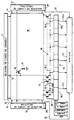
- the Figure shows an embodiment preferential.
- a liquid crystal display 10 includes a data line scanner 11 which provides data signals on a plurality of lines of data 12.
- a selection line scanner 13 applies sequentially a voltage on a plurality of lines of selection 14.
- Data lines 12 and data lines selection 14 are perpendicular and the cells to liquid crystals, like 15, are arranged at crosses.
- Switching devices 16, such as thin film transistors (TFT) are put under voltage by the polarized selection lines 14 and the 12 data lines load crystal cells liquids at levels determined by the signals of data.
- a redundant selection line scanner 13 can also apply tension to selection lines 14.
- the stages of the selection line scanner 13 which correspond to the defective stages of the sweeper 13 of selection lines are used instead of floors defective.
- Data line scanner 11, data line scanner 13 selection lines and the TFT 16 are manufactured simultaneously on an insulating substrate.
- test transistors 17, which are preferably TFTs are produced on the substrate at the same time as the scanners 11, 13 and the TFTs 16.
- the conductive connection of a TFT 17 is arranged between each of the data lines 12 and an output bus 18.
- the output bus 18 is divided into 6 games, 18-1 to 18-6.
- a shift register 19 includes preferably a number of parts 19-1 to 19-6, equal to number of parts in the output bus 18.
- the lines of output 20 of the shift register 19 are connected separately to the TFT 17 control electrodes.
- test lines 21-1 to 21-6 connect parts 18-1 to 18-6 from the bus, respectively, to a monitor 22.
- the lines input 23 to 27 are used to supply the voltage of polarization, input signal and clock signals shift register 19.
- the operating speed of the shift register 19 is increased, and the load on the data scanner 11 is decreased by dividing bus 18.
- Selection line sweepers 13 and 13 ' each include an additional floor, respectively 28 and 28 '.
- the sweepers 13 and 13 'of selection lines are tested separately before continuity test, short circuit test, and test of the data line scanner described here by doing operate the selection line sweeper so normal and looking at the monitor 22.
- a defective floor is indicated by the absence of an input signal to the monitor 22 coming from test line 24 of the floor sweeper defective.
- Separate equipment and methods such as described in patent applications S / N 660274 and S / N 660273, to which reference has been made above, can be used to identify the faulty floor.
- the shift registers 19 set sequentially energized the transistors 17 when the 11 data line scanner provides signals from data on data lines 12. Only one of the TFTs 17 is energized both in each register part and therefore the data lines 12 are coupled in sequence to monitor 22 via individual TFTs 17 and part of the bus 18. Consequently, the absence of voltage on one of the test lines 21-1 to 21-6 indicates a lack of continuity of one of the data lines 12.
- the faulty data line can be identified with precision if you synchronize the operation of the sweeper 11 data lines and shift register 19 and if the sequential implementation of the TFTs 17 is monitored.
- the monitor 22 therefore preferably comprises equipment for computer-controlled measurement, which is the skill technical specialists. The defective floors of the data line sweepers are identified because that no stage after the defective stage gives a signal on a data line 12.
- the existence of a short circuit between one of the lines of data 12 and one of the selection lines 14 is detected using the selection line sweeper 13 to sequentially activate selection lines 14 all by switching on the TFT 17.
- the result of a short circuit between a selection line and a line of data is the application by one of the test lines 21-1 at 21-6 of a voltage at monitor 22.
- the identity of data lines and shorted selection lines can be determined precisely.
- the preferred embodiment includes the six output lines 21, the two test lines 24, 24 'and the five input lines 23-27, thirteen lines in total. This is a very significant reduction in the number of lines of test necessary to directly test the lines of data 12 separately, which would require a line of separate test for each column of crystal cells liquids, 1,440 lines in the example given above.
Landscapes
- Physics & Mathematics (AREA)
- General Physics & Mathematics (AREA)
- Engineering & Computer Science (AREA)
- Computer Hardware Design (AREA)
- Theoretical Computer Science (AREA)
- General Engineering & Computer Science (AREA)
- Liquid Crystal (AREA)
- Liquid Crystal Display Device Control (AREA)
- Testing Of Short-Circuits, Discontinuities, Leakage, Or Incorrect Line Connections (AREA)
- Testing Electric Properties And Detecting Electric Faults (AREA)
- Tests Of Electronic Circuits (AREA)
- Control Of Indicators Other Than Cathode Ray Tubes (AREA)
Abstract
Description
Claims (7)
- Circuit de test intégré d'un afficheur à cristaux liquides (10) ayant une matrice de cellules disposées en rangées et colonnes, une pluralité de lignes de données (12) pour appliquer des signaux de données venant d'un balayeur de lignes de données (11) aux colonnes de cellules et une pluralité de lignes de sélection (14) pour appliquer des signaux de sélection venant d'un balayeur de lignes de sélection (13,13') aux rangées de cellules, caractérisé en ce qu'il comporte:un bus de sortie (18) ayant au moins une ligne de test (21-1à6),une pluralité de dispositifs semi-conducteurs (17) ayant des liaisons conductrices reliant séparément les lignes de données (12) au bus de sortie (18), chacun des dispositifs semi-conducteurs (17) ayant une électrode de commande,des moyens (20) pour actionner séquentiellement les électrodes de commande pour transférer lesdits signaux de données des lignes de données (12) à ladite ligne de test (21-1à6),et des moyens (22) pour surveiller la ligne de test afin d'identifier les lignes de données (12) ouvertes et les lignes de sélection (14) en court-circuit.
- Circuit de test selon la revendication 1 caractérisé en ce que le bus de sortie (18) est divisé en une pluralité de segments (18-1à6), chacun de ces segments ayant une ligne de test (21-1à6), et en ce que les moyens (20) pour actionner séquentiellement les électrodes de commande comprennent un registre à décalage (19) divisé en un nombre égal de sections (19-1à6) où chacune des sections actionne l'un des segments (18-1à6).
- Circuit de test selon la revendication 2 caractérisé en ce que le balayeur de lignes de sélection (13,13') inclut un étage de test (28,28') pour isoler le balayeur de lignes de sélection (13,13') du circuit de test, cet étage de test (28,28') ayant une ligne de sortie de test (24,24') pour vérifier le fonctionnement du balayeur de lignes de sélection (13,13').
- Circuit de test selon la revendication 3 caractérisé en ce que les dispositifs semi-conducteurs (17) sont des transistors à couches minces.
- Méthode de test d'un afficheur à cristaux liquides (10) ayant une matrice de cellules disposées en rangées et colonnes, l'afficheur (10) ayant un balayeur de lignes de données (11) pour appliquer les signaux de données à une pluralité de lignes de données (12) qui appliquent individuellement des signaux de données aux colonnes, l'afficheur (10) ayant aussi un balayeur de lignes de sélection (13,13') pour appliquer des signaux de sélection à une pluralité de lignes de sélection (14) qui appliquent séparément des signaux de sélection aux rangées, caractérisée en ce qu'elle est appliquée au dispositif selon une quelconque des revendications précédentes, et qu'elle comporte dans un ordre quelconque les étapes suivantes:arrangement de dispositifs semi-conducteurs (17) séparés entre chacune des lignes de données (12) et un bus (18),mise en oeuvre séquentielle des dispositifs semi-conducteurs (17) pendant l'application de signaux de données aux lignes de données (12) et surveillance de la tension sur le bus (18) pour identifier les lignes de données (12) ouvertes par l'absence de tension sur le bus (18).actionnement séquentiel des dispositifs semi-conducteurs (17) pendant l'application de signaux de sélection aux lignes de sélection (14) tout en surveillant le bus (18) pour détecter l'existence d'un court-circuit par l'existence d'une tension sur le bus (18),et fonctionnement de manière normale du balayeur de lignes de données (13,13') afin de détecter un étage défectueux par l'absence de signal sur le moniteur (22).
- Méthode selon la revendication 5 incluant aussi l'étape de division du bus (18) en une pluralité de segments (18-1à6) et en surveillant séparément les segments (18-1à6).
- Méthode selon la revendication 6 caractérisée en ce que les dispositifs semi-conducteurs (17) sont des transistors à couches minces.
Applications Claiming Priority (3)
| Application Number | Priority Date | Filing Date | Title |
|---|---|---|---|
| US660275 | 1991-02-28 | ||
| US07/660,275 US5113134A (en) | 1991-02-28 | 1991-02-28 | Integrated test circuit for display devices such as LCD's |
| PCT/FR1992/000188 WO1992015891A1 (fr) | 1991-02-28 | 1992-02-28 | Circuit de test integre pour dispositifs d'affichage tels que des afficheurs a cristaux liquides |
Publications (2)
| Publication Number | Publication Date |
|---|---|
| EP0584087A1 EP0584087A1 (fr) | 1994-03-02 |
| EP0584087B1 true EP0584087B1 (fr) | 2000-03-08 |
Family
ID=24648835
Family Applications (1)
| Application Number | Title | Priority Date | Filing Date |
|---|---|---|---|
| EP92907297A Expired - Lifetime EP0584087B1 (fr) | 1991-02-28 | 1992-02-28 | Circuit de test integre pour dispositifs d'affichage tels que des afficheurs a cristaux liquides |
Country Status (6)
| Country | Link |
|---|---|
| US (1) | US5113134A (fr) |
| EP (1) | EP0584087B1 (fr) |
| JP (1) | JP3213943B2 (fr) |
| KR (1) | KR100212108B1 (fr) |
| DE (1) | DE69230754T2 (fr) |
| WO (1) | WO1992015891A1 (fr) |
Families Citing this family (54)
| Publication number | Priority date | Publication date | Assignee | Title |
|---|---|---|---|---|
| US5179345A (en) * | 1989-12-13 | 1993-01-12 | International Business Machines Corporation | Method and apparatus for analog testing |
| FR2667718B1 (fr) * | 1990-10-09 | 1992-11-27 | France Etat | Circuit de commande des colonnes d'un ecran d'affichage, comprenant des moyens de test a sortie unique. |
| JP2792634B2 (ja) * | 1991-06-28 | 1998-09-03 | シャープ株式会社 | アクティブマトリクス基板の検査方法 |
| US5268638A (en) * | 1991-07-15 | 1993-12-07 | Siemens Aktiengesellschaft | Method for particle beam testing of substrates for liquid crystal displays "LCD" |
| US5543729A (en) * | 1991-09-10 | 1996-08-06 | Photon Dynamics, Inc. | Testing apparatus and connector for liquid crystal display substrates |
| US5184082A (en) * | 1991-09-18 | 1993-02-02 | Honeywell Inc. | Apparatus and method for testing an active matrix pixel display |
| JP2758103B2 (ja) * | 1992-04-08 | 1998-05-28 | シャープ株式会社 | アクティブマトリクス基板及びその製造方法 |
| GB9219836D0 (en) * | 1992-09-18 | 1992-10-28 | Philips Electronics Uk Ltd | Electronic drive circuits for active matrix devices,and a method of self-tasting and programming such circuits |
| US5483155A (en) * | 1992-11-20 | 1996-01-09 | Eastman Kodak Company | Test system and method for dynamic testing of a plurality of packaged same-type charge coupled device image sensors |
| US5546013A (en) * | 1993-03-05 | 1996-08-13 | International Business Machines Corporation | Array tester for determining contact quality and line integrity in a TFT/LCD |
| JP3402400B2 (ja) | 1994-04-22 | 2003-05-06 | 株式会社半導体エネルギー研究所 | 半導体集積回路の作製方法 |
| US6943764B1 (en) | 1994-04-22 | 2005-09-13 | Semiconductor Energy Laboratory Co., Ltd. | Driver circuit for an active matrix display device |
| US6919874B1 (en) | 1994-05-17 | 2005-07-19 | Thales Avionics Lcd S.A. | Shift register using M.I.S. transistors and supplementary column |
| JP2889132B2 (ja) * | 1994-10-12 | 1999-05-10 | 株式会社フロンテック | 薄膜トランジスタの検査装置 |
| CN100576306C (zh) * | 1995-02-01 | 2009-12-30 | 精工爱普生株式会社 | 液晶显示装置 |
| US5686935A (en) * | 1995-03-06 | 1997-11-11 | Thomson Consumer Electronics, S.A. | Data line drivers with column initialization transistor |
| US5600345A (en) * | 1995-03-06 | 1997-02-04 | Thomson Consumer Electronics, S.A. | Amplifier with pixel voltage compensation for a display |
| DE69623153T2 (de) * | 1995-03-06 | 2003-04-17 | Thomson Multimedia, Boulogne | Treiberschaltungen für Datenleitungen mit einem gemeinsamen Rampensignal für ein Anzeigesystem |
| US5673063A (en) * | 1995-03-06 | 1997-09-30 | Thomson Consumer Electronics, S.A. | Data line driver for applying brightness signals to a display |
| US5726678A (en) * | 1995-03-06 | 1998-03-10 | Thomson Consumer Electronics, S.A. | Signal disturbance reduction arrangement for a liquid crystal display |
| JP3251474B2 (ja) * | 1995-09-06 | 2002-01-28 | シャープ株式会社 | アクティブマトリクス基板 |
| JP3190238B2 (ja) * | 1995-10-31 | 2001-07-23 | シャープ株式会社 | アクティブマトリクス液晶パネルの欠陥検出方法 |
| KR100195276B1 (ko) * | 1995-12-01 | 1999-06-15 | 윤종용 | 구동회로를 내장한 액정 표시장치 및 그 구동방법 |
| JPH09159997A (ja) * | 1995-12-07 | 1997-06-20 | Sharp Corp | 液晶パネルの欠陥候補箇所検出方法 |
| US6697037B1 (en) | 1996-04-29 | 2004-02-24 | International Business Machines Corporation | TFT LCD active data line repair |
| DE19710855A1 (de) * | 1997-03-15 | 1998-10-01 | Dambach Werke Gmbh | Leuchtdiodenmatrix-Anzeigevorrichtung |
| JPH10260391A (ja) * | 1997-03-19 | 1998-09-29 | Fujitsu Ltd | 検査回路を有する液晶表示装置 |
| US6518945B1 (en) * | 1997-07-25 | 2003-02-11 | Aurora Systems, Inc. | Replacing defective circuit elements by column and row shifting in a flat-panel display |
| US6265889B1 (en) * | 1997-09-30 | 2001-07-24 | Kabushiki Kaisha Toshiba | Semiconductor test circuit and a method for testing a semiconductor liquid crystal display circuit |
| US6191770B1 (en) * | 1997-12-11 | 2001-02-20 | Lg. Philips Lcd Co., Ltd. | Apparatus and method for testing driving circuit in liquid crystal display |
| JP3107039B2 (ja) * | 1998-03-20 | 2000-11-06 | 日本電気株式会社 | 面光源プローバ装置及び検査方法 |
| US6424161B2 (en) * | 1998-09-03 | 2002-07-23 | Micron Technology, Inc. | Apparatus and method for testing fuses |
| US6281701B1 (en) * | 1999-06-04 | 2001-08-28 | Chi Mei Optoelectronics Corporation | Apparatus for testing flat panel display |
| JP2001330639A (ja) * | 2000-05-24 | 2001-11-30 | Toshiba Corp | アレイ基板の検査方法 |
| JP4615100B2 (ja) * | 2000-07-18 | 2011-01-19 | 富士通セミコンダクター株式会社 | データドライバ及びそれを用いた表示装置 |
| JP4276373B2 (ja) | 2000-12-07 | 2009-06-10 | セイコーエプソン株式会社 | 電気光学装置の検査用回路、電気光学装置および電子機器 |
| KR100442305B1 (ko) * | 2001-07-18 | 2004-07-30 | 가부시끼가이샤 도시바 | 어레이 기판 및 그 검사 방법 및 액정 표시 장치 |
| JP3707404B2 (ja) * | 2001-08-03 | 2005-10-19 | ソニー株式会社 | 検査方法、半導体装置、及び表示装置 |
| JP3989756B2 (ja) * | 2002-03-18 | 2007-10-10 | シャープ株式会社 | 表示装置およびその走査回路検査方法 |
| JP4103544B2 (ja) * | 2002-10-28 | 2008-06-18 | セイコーエプソン株式会社 | 有機el装置 |
| KR100517558B1 (ko) | 2003-03-17 | 2005-09-28 | 삼성전자주식회사 | 테스트 핀을 구비한 반도체 집적 회로 및 그것의 테스트방법 |
| TW594655B (en) * | 2003-07-11 | 2004-06-21 | Toppoly Optoelectronics Corp | Testing circuit and method thereof for a flat panel display |
| JP2005043661A (ja) * | 2003-07-22 | 2005-02-17 | Sony Corp | 検査方法、半導体装置、及び表示装置 |
| JP4143588B2 (ja) * | 2003-10-27 | 2008-09-03 | 日本電気株式会社 | 出力回路及びデジタルアナログ回路並びに表示装置 |
| KR101133768B1 (ko) * | 2005-03-07 | 2012-04-09 | 삼성전자주식회사 | 표시 장치 |
| JP4887977B2 (ja) * | 2005-11-21 | 2012-02-29 | セイコーエプソン株式会社 | 電気光学装置、電気光学装置の駆動方法、電圧モニタ方法および電子機器 |
| DE102006005051A1 (de) * | 2006-02-03 | 2007-08-16 | Siemens Ag | Schaltungsanordnung und Prüfvorrichtung |
| KR101337459B1 (ko) * | 2006-02-03 | 2013-12-06 | 가부시키가이샤 한도오따이 에네루기 켄큐쇼 | 표시장치 및 그 표시장치를 구비한 전자기기 |
| CN104183225B (zh) * | 2014-08-15 | 2017-08-15 | 上海天马微电子有限公司 | 一种驱动装置、阵列基板和显示装置 |
| WO2017094461A1 (fr) * | 2015-12-01 | 2017-06-08 | シャープ株式会社 | Élément de formation d'image |
| KR102510912B1 (ko) * | 2018-03-19 | 2023-03-17 | 삼성디스플레이 주식회사 | 표시 장치 및 이의 크랙 검사 방법 |
| JP7096721B2 (ja) * | 2018-07-13 | 2022-07-06 | 株式会社ジャパンディスプレイ | 表示装置 |
| US11508274B2 (en) * | 2020-06-30 | 2022-11-22 | Silicon Works Co., Ltd. | Display panel driving device |
| CN113763850A (zh) * | 2021-09-14 | 2021-12-07 | 深圳创维-Rgb电子有限公司 | 不良竖线定位电路、方法、显示模组及电视机 |
Family Cites Families (13)
| Publication number | Priority date | Publication date | Assignee | Title |
|---|---|---|---|---|
| US4297692A (en) * | 1979-03-07 | 1981-10-27 | Simmonds Precision Products, Inc. | Segment failure detector for digital display |
| DE2951584A1 (de) * | 1979-12-21 | 1981-07-16 | Kienzle Apparate Gmbh, 7730 Villingen-Schwenningen | Verfahren und anordnung zur ansteuerung, ueberwachung und kontrolle des betriebes einer weitgehend passiven datenanzeige, insbesondere z.b. einer fluessigkristallanzeige (lcd-anzeige) |
| GB2081018B (en) * | 1980-07-31 | 1985-06-26 | Suwa Seikosha Kk | Active matrix assembly for display device |
| FR2554622B1 (fr) * | 1983-11-03 | 1988-01-15 | Commissariat Energie Atomique | Procede de fabrication d'une matrice de composants electroniques |
| US4701695A (en) * | 1983-12-22 | 1987-10-20 | Monolithic Memories, Inc. | Short detector for PROMS |
| DE3432247C2 (de) * | 1984-09-01 | 1986-12-18 | Mannesmann Kienzle GmbH, 7730 Villingen-Schwenningen | Anordnung zur Anzeige einer fehlerhaften Funktionsweise einer Flüssigkristallanzeige |
| US4766430A (en) * | 1986-12-19 | 1988-08-23 | General Electric Company | Display device drive circuit |
| US4742346A (en) * | 1986-12-19 | 1988-05-03 | Rca Corporation | System for applying grey scale codes to the pixels of a display device |
| NL8700933A (nl) * | 1987-04-21 | 1988-11-16 | Philips Nv | Testmethode voor lcd-elementen. |
| KR960006869B1 (ko) * | 1987-09-02 | 1996-05-23 | 도오교오 에레구토론 가부시끼가이샤 | 프로우브 장치에 의한 전기특성 검사방법 |
| US4893311A (en) * | 1988-04-25 | 1990-01-09 | Motorola, Inc. | CMOS implementation of a built-in self test input generator (BISTIG) |
| US4870357A (en) * | 1988-06-03 | 1989-09-26 | Apple Computer, Inc. | LCD error detection system |
| US5057775A (en) * | 1990-05-04 | 1991-10-15 | Genrad, Inc. | Method of testing control matrices for flat-panel displays |
-
1991
- 1991-02-28 US US07/660,275 patent/US5113134A/en not_active Expired - Lifetime
-
1992
- 1992-02-28 KR KR1019930702537A patent/KR100212108B1/ko not_active Expired - Fee Related
- 1992-02-28 DE DE69230754T patent/DE69230754T2/de not_active Expired - Fee Related
- 1992-02-28 JP JP50690092A patent/JP3213943B2/ja not_active Expired - Fee Related
- 1992-02-28 WO PCT/FR1992/000188 patent/WO1992015891A1/fr not_active Ceased
- 1992-02-28 EP EP92907297A patent/EP0584087B1/fr not_active Expired - Lifetime
Also Published As
| Publication number | Publication date |
|---|---|
| WO1992015891A1 (fr) | 1992-09-17 |
| US5113134A (en) | 1992-05-12 |
| KR930703616A (ko) | 1993-11-30 |
| DE69230754T2 (de) | 2000-06-29 |
| KR100212108B1 (ko) | 1999-08-02 |
| DE69230754D1 (de) | 2000-04-13 |
| EP0584087A1 (fr) | 1994-03-02 |
| JP3213943B2 (ja) | 2001-10-02 |
| JPH06505799A (ja) | 1994-06-30 |
Similar Documents
| Publication | Publication Date | Title |
|---|---|---|
| WO1992015891A1 (fr) | Circuit de test integre pour dispositifs d'affichage tels que des afficheurs a cristaux liquides | |
| EP0321073B1 (fr) | Dispositif d'affichage à cristal liquide | |
| EP0506906B1 (fr) | Systeme pour appliquer des signaux de luminosite a un dispositif | |
| JP2984712B2 (ja) | 表示装置検査方法 | |
| EP0627722B1 (fr) | Valve de lumière avec circuit pour la détection de défauts | |
| JP2810844B2 (ja) | Tft/lcdアレイをテストする方法 | |
| FR2704321A1 (fr) | Appareil et procédé de détection d'erreur pour un affichage électro-optique. | |
| EP0506875A1 (fr) | Ecran a cristaux liquides avec redondance du lecteur de selection. | |
| WO1992015992A1 (fr) | Registre a decalage utilise comme balayeur de lignes de selection pour un afficheur a cristaux liquides | |
| IE914093A1 (en) | Method and apparatus for testing lcd panel array prior to¹shorting bar removal | |
| US20010028336A1 (en) | Semiconductor integrated circuit for driving liquid crystal panel | |
| JP4112300B2 (ja) | 電気的検査方法及び半導体表示装置の作製方法 | |
| JP3790684B2 (ja) | 検査用回路、検査方法および液晶セルの製造方法 | |
| US7423447B2 (en) | Method for testing liquid crystal display panels | |
| EP0573607B1 (fr) | Registres a decalage redondants pour dispositifs de balayage | |
| FR2667188A1 (fr) | Circuit echantillonneur-bloqueur pour ecran d'affichage a cristal liquide. | |
| JP3191073B2 (ja) | 多結晶シリコン薄膜トランジスタアレイ検査装置 | |
| EP0573550A1 (fr) | Procede de test pour les registres a decalage redondants | |
| JPH01102498A (ja) | アクティブマトリックス基板の試験方法 | |
| JPH06281944A (ja) | 修復可能の冗長駆動マトリックス表示装置 | |
| JPH0646345B2 (ja) | アクテイブマトリクス基板 | |
| JP3191898B2 (ja) | 薄膜トランジスタアレイの検査方法 | |
| JP2558755B2 (ja) | 液晶表示パネル用セグメントドライブic | |
| JPH079521B2 (ja) | 点欠陥の検出及び補修の可能なアクティブマトリクス基板の製造方法 | |
| JP2558845B2 (ja) | 液晶パネル駆動用集積回路 |
Legal Events
| Date | Code | Title | Description |
|---|---|---|---|
| PUAI | Public reference made under article 153(3) epc to a published international application that has entered the european phase |
Free format text: ORIGINAL CODE: 0009012 |
|
| 17P | Request for examination filed |
Effective date: 19930727 |
|
| AK | Designated contracting states |
Kind code of ref document: A1 Designated state(s): DE FR GB NL |
|
| 17Q | First examination report despatched |
Effective date: 19940809 |
|
| RIC1 | Information provided on ipc code assigned before grant |
Free format text: 6G 01R 31/02 A, 6G 01R 31/28 B |
|
| GRAG | Despatch of communication of intention to grant |
Free format text: ORIGINAL CODE: EPIDOS AGRA |
|
| GRAG | Despatch of communication of intention to grant |
Free format text: ORIGINAL CODE: EPIDOS AGRA |
|
| GRAG | Despatch of communication of intention to grant |
Free format text: ORIGINAL CODE: EPIDOS AGRA |
|
| GRAH | Despatch of communication of intention to grant a patent |
Free format text: ORIGINAL CODE: EPIDOS IGRA |
|
| GRAH | Despatch of communication of intention to grant a patent |
Free format text: ORIGINAL CODE: EPIDOS IGRA |
|
| GRAA | (expected) grant |
Free format text: ORIGINAL CODE: 0009210 |
|
| AK | Designated contracting states |
Kind code of ref document: B1 Designated state(s): DE FR GB NL |
|
| GBT | Gb: translation of ep patent filed (gb section 77(6)(a)/1977) |
Effective date: 20000308 |
|
| REF | Corresponds to: |
Ref document number: 69230754 Country of ref document: DE Date of ref document: 20000413 |
|
| PLBE | No opposition filed within time limit |
Free format text: ORIGINAL CODE: 0009261 |
|
| 26N | No opposition filed | ||
| REG | Reference to a national code |
Ref country code: GB Ref legal event code: IF02 |
|
| PGFP | Annual fee paid to national office [announced via postgrant information from national office to epo] |
Ref country code: NL Payment date: 20040205 Year of fee payment: 13 |
|
| PG25 | Lapsed in a contracting state [announced via postgrant information from national office to epo] |
Ref country code: NL Free format text: LAPSE BECAUSE OF NON-PAYMENT OF DUE FEES Effective date: 20050901 |
|
| NLV4 | Nl: lapsed or anulled due to non-payment of the annual fee |
Effective date: 20050901 |
|
| PGFP | Annual fee paid to national office [announced via postgrant information from national office to epo] |
Ref country code: DE Payment date: 20080221 Year of fee payment: 17 |
|
| PGFP | Annual fee paid to national office [announced via postgrant information from national office to epo] |
Ref country code: GB Payment date: 20090225 Year of fee payment: 18 |
|
| PGFP | Annual fee paid to national office [announced via postgrant information from national office to epo] |
Ref country code: FR Payment date: 20090213 Year of fee payment: 18 |
|
| PG25 | Lapsed in a contracting state [announced via postgrant information from national office to epo] |
Ref country code: DE Free format text: LAPSE BECAUSE OF NON-PAYMENT OF DUE FEES Effective date: 20090901 |
|
| GBPC | Gb: european patent ceased through non-payment of renewal fee |
Effective date: 20100228 |
|
| REG | Reference to a national code |
Ref country code: FR Ref legal event code: ST Effective date: 20101029 |
|
| PG25 | Lapsed in a contracting state [announced via postgrant information from national office to epo] |
Ref country code: FR Free format text: LAPSE BECAUSE OF NON-PAYMENT OF DUE FEES Effective date: 20100301 |
|
| PG25 | Lapsed in a contracting state [announced via postgrant information from national office to epo] |
Ref country code: GB Free format text: LAPSE BECAUSE OF NON-PAYMENT OF DUE FEES Effective date: 20100228 |