EP0338817A2 - Integrierte Halbleiterschaltungsanordnung vom "Masterslice"-Typ und Herstellungsverfahren dafür - Google Patents
Integrierte Halbleiterschaltungsanordnung vom "Masterslice"-Typ und Herstellungsverfahren dafür Download PDFInfo
- Publication number
- EP0338817A2 EP0338817A2 EP89303912A EP89303912A EP0338817A2 EP 0338817 A2 EP0338817 A2 EP 0338817A2 EP 89303912 A EP89303912 A EP 89303912A EP 89303912 A EP89303912 A EP 89303912A EP 0338817 A2 EP0338817 A2 EP 0338817A2
- Authority
- EP
- European Patent Office
- Prior art keywords
- region
- region corresponding
- wiring
- wirings
- impurity regions
- Prior art date
- Legal status (The legal status is an assumption and is not a legal conclusion. Google has not performed a legal analysis and makes no representation as to the accuracy of the status listed.)
- Granted
Links
- 239000004065 semiconductor Substances 0.000 title claims abstract description 14
- 238000000034 method Methods 0.000 title claims description 34
- 238000013459 approach Methods 0.000 title claims description 23
- 238000009413 insulation Methods 0.000 claims abstract description 73
- 238000003491 array Methods 0.000 claims abstract description 12
- 239000012535 impurity Substances 0.000 claims description 143
- 238000000926 separation method Methods 0.000 claims description 37
- 238000009792 diffusion process Methods 0.000 claims description 7
- 238000010586 diagram Methods 0.000 description 38
- 230000008569 process Effects 0.000 description 19
- 230000008901 benefit Effects 0.000 description 10
- 230000009467 reduction Effects 0.000 description 8
- 230000002457 bidirectional effect Effects 0.000 description 5
- 239000000470 constituent Substances 0.000 description 4
- 230000002194 synthesizing effect Effects 0.000 description 4
- VYPSYNLAJGMNEJ-UHFFFAOYSA-N Silicium dioxide Chemical compound O=[Si]=O VYPSYNLAJGMNEJ-UHFFFAOYSA-N 0.000 description 3
- 230000005540 biological transmission Effects 0.000 description 3
- 230000010354 integration Effects 0.000 description 3
- 238000000059 patterning Methods 0.000 description 3
- 229910052814 silicon oxide Inorganic materials 0.000 description 3
- 230000015572 biosynthetic process Effects 0.000 description 2
- 238000005229 chemical vapour deposition Methods 0.000 description 2
- 230000003247 decreasing effect Effects 0.000 description 2
- 230000006870 function Effects 0.000 description 2
- 238000012986 modification Methods 0.000 description 2
- 230000004048 modification Effects 0.000 description 2
- 239000000758 substrate Substances 0.000 description 2
- XAGFODPZIPBFFR-UHFFFAOYSA-N aluminium Chemical compound [Al] XAGFODPZIPBFFR-UHFFFAOYSA-N 0.000 description 1
- 229910052782 aluminium Inorganic materials 0.000 description 1
- 238000013461 design Methods 0.000 description 1
- 230000000694 effects Effects 0.000 description 1
- 230000005611 electricity Effects 0.000 description 1
- 238000005530 etching Methods 0.000 description 1
- 230000008020 evaporation Effects 0.000 description 1
- 238000001704 evaporation Methods 0.000 description 1
- 230000003071 parasitic effect Effects 0.000 description 1
- 239000005360 phosphosilicate glass Substances 0.000 description 1
- 229910021420 polycrystalline silicon Inorganic materials 0.000 description 1
- 229920005591 polysilicon Polymers 0.000 description 1
- 238000012545 processing Methods 0.000 description 1
- 238000009751 slip forming Methods 0.000 description 1
- 239000007787 solid Substances 0.000 description 1
- 230000003068 static effect Effects 0.000 description 1
Images


Classifications
-
- H—ELECTRICITY
- H01—ELECTRIC ELEMENTS
- H01L—SEMICONDUCTOR DEVICES NOT COVERED BY CLASS H10
- H01L27/00—Devices consisting of a plurality of semiconductor or other solid-state components formed in or on a common substrate
- H01L27/02—Devices consisting of a plurality of semiconductor or other solid-state components formed in or on a common substrate including semiconductor components specially adapted for rectifying, oscillating, amplifying or switching and having potential barriers; including integrated passive circuit elements having potential barriers
- H01L27/04—Devices consisting of a plurality of semiconductor or other solid-state components formed in or on a common substrate including semiconductor components specially adapted for rectifying, oscillating, amplifying or switching and having potential barriers; including integrated passive circuit elements having potential barriers the substrate being a semiconductor body
-
- H—ELECTRICITY
- H01—ELECTRIC ELEMENTS
- H01L—SEMICONDUCTOR DEVICES NOT COVERED BY CLASS H10
- H01L23/00—Details of semiconductor or other solid state devices
- H01L23/52—Arrangements for conducting electric current within the device in operation from one component to another, i.e. interconnections, e.g. wires, lead frames
- H01L23/522—Arrangements for conducting electric current within the device in operation from one component to another, i.e. interconnections, e.g. wires, lead frames including external interconnections consisting of a multilayer structure of conductive and insulating layers inseparably formed on the semiconductor body
- H01L23/528—Geometry or layout of the interconnection structure
-
- H—ELECTRICITY
- H01—ELECTRIC ELEMENTS
- H01L—SEMICONDUCTOR DEVICES NOT COVERED BY CLASS H10
- H01L21/00—Processes or apparatus adapted for the manufacture or treatment of semiconductor or solid state devices or of parts thereof
- H01L21/70—Manufacture or treatment of devices consisting of a plurality of solid state components formed in or on a common substrate or of parts thereof; Manufacture of integrated circuit devices or of parts thereof
- H01L21/77—Manufacture or treatment of devices consisting of a plurality of solid state components or integrated circuits formed in, or on, a common substrate
- H01L21/78—Manufacture or treatment of devices consisting of a plurality of solid state components or integrated circuits formed in, or on, a common substrate with subsequent division of the substrate into plural individual devices
- H01L21/82—Manufacture or treatment of devices consisting of a plurality of solid state components or integrated circuits formed in, or on, a common substrate with subsequent division of the substrate into plural individual devices to produce devices, e.g. integrated circuits, each consisting of a plurality of components
-
- H—ELECTRICITY
- H01—ELECTRIC ELEMENTS
- H01L—SEMICONDUCTOR DEVICES NOT COVERED BY CLASS H10
- H01L27/00—Devices consisting of a plurality of semiconductor or other solid-state components formed in or on a common substrate
- H01L27/02—Devices consisting of a plurality of semiconductor or other solid-state components formed in or on a common substrate including semiconductor components specially adapted for rectifying, oscillating, amplifying or switching and having potential barriers; including integrated passive circuit elements having potential barriers
- H01L27/04—Devices consisting of a plurality of semiconductor or other solid-state components formed in or on a common substrate including semiconductor components specially adapted for rectifying, oscillating, amplifying or switching and having potential barriers; including integrated passive circuit elements having potential barriers the substrate being a semiconductor body
- H01L27/10—Devices consisting of a plurality of semiconductor or other solid-state components formed in or on a common substrate including semiconductor components specially adapted for rectifying, oscillating, amplifying or switching and having potential barriers; including integrated passive circuit elements having potential barriers the substrate being a semiconductor body including a plurality of individual components in a repetitive configuration
- H01L27/118—Masterslice integrated circuits
- H01L27/11803—Masterslice integrated circuits using field effect technology
- H01L27/11807—CMOS gate arrays
-
- H—ELECTRICITY
- H01—ELECTRIC ELEMENTS
- H01L—SEMICONDUCTOR DEVICES NOT COVERED BY CLASS H10
- H01L2924/00—Indexing scheme for arrangements or methods for connecting or disconnecting semiconductor or solid-state bodies as covered by H01L24/00
- H01L2924/0001—Technical content checked by a classifier
- H01L2924/0002—Not covered by any one of groups H01L24/00, H01L24/00 and H01L2224/00
Definitions
- the present invention relates to a technique of utilizing a master slice approach and, more particularly, to a semiconductor integrated circuit device and a method of producing the device using the master slice approach.
- a semiconductor integrated circuit or large scale integrated circuit device produced through the master slice approach is hereinafter referred to as a master slice type LSI device.
- the master slice approach generally comprises a first process of forming a master chip and a second process of forming a desired wiring pattern on the master chip.
- a basic cell region including a plurality of basic cells, each consisting of a predetermined number of transistors, is formed together with an input/output (I/O) cell region on a chip using a common and fixed pattern mask.
- the second process is carried out in accordance with a specification or conditions demanded by a user and includes a plurality of steps.
- the second process normally includes four steps of: forming contact holes in a first insulation layer formed on the master chip; forming thereon a first wiring layer; forming through holes in a second insulation layer formed thereon; and forming thereon a second wiring layer so as to contact the first wiring layer via through holes. Therefore, four pattern masks corresponding to the contact hole, first wiring layer, through hole and second wiring layer are required to constitute a given circuit in the basic cell region.
- This one custom mask approach is a method of forming a wiring pattern on the master chip using one layer custom mask (wiring pattern mask according to user's specification).
- wiring pattern mask according to user's specification.
- the wiring pattern mask can be made common to a plurality of master slice type LSI devices, it becomes possible to easily realize the reduction of the turnaround time and the simplification of the process.
- An embodiment of the present invention may provide a master slice type LSI device and a method of producing the device which can greatly reduce a turnaround time.
- An embodiment of the present invention may apply the one custom mask approach to an I/O cell region of a master chip, thereby producing a desired master slice type LSI device easily and in a short period.
- Another embodiment of the present invention may apply the one custom mask approach to a basic cell region of a master chip and utilize an unused region on the basic cell region so as to form a wiring pattern for bypassing a wiring obstruction pattern, thereby producing a desired master slice type LSI device easily and in a short period.
- a semiconductor integrated circuit device including: a master chip including a plurality of basic cells arrayed thereon, each having a plurality of wiring channels extending along a first direction and a second direction perpendicular to the first direction and including: a pair of electrodes extending in parallel along the second direction; a separation region formed in a region corresponding to a central portion of the electrodes; a p-type impurity region formed on one side of the separation region with respect to the first direction, having a first, second and third regions formed on one side of the electrodes with respect to the second direction, on another side thereof and therebetween, respectively; an n-type impurity region formed on another side of the separation region, having a fourth, fifth and sixth regions formed on one side of the electrodes with respect to the second direction, on another side thereof and therebetween, respectively; and six lead portions formed by a portion of the pair of electrodes, having four lead portions formed in each end portion thereof and two lead portions formed in each central portion
- a semiconductor integrated circuit device comprising: a master chip including a basic cell region having a plurality of basic cell arrays arranged thereon, and an input/output cell region having a plurality of input/output cells arranged along the periphery of the basic cell region; a first wiring layer formed on the basic cell region and the input/output cell region via a first insulation layer having contact holes at predetermined positions; and a second wiring layer formed on the first wiring layer via a second insulation layer having through holes at predetermined positions; wherein the first wiring layer includes fixed wirings in a region corresponding to the input/output cell region, and the second wiring layer includes wirings programmed in accordance with conditions of a given circuit applied to the input/output cell region in a region corresponding to the input/output cell region.
- a semiconductor integrated circuit device including: a master chip including a basic cell region having a plurality of basic cell arrays arranged thereon and extending along a first direction at a constant space therebetween, and in input/output cell region having a plurality of input/output cells arranged along the periphery of the basic cell region; a first wiring layer formed on the basic cell region and the input/output cell region via a first insulation layer having contact holes at predetermined positions; and a second wiring layer formed on the first wiring layer via a second insulation layer having through holes at predetermined positions; wherein the first wiring layer includes fixed wirings in a region corresponding to the basic cell region, and a bypass wiring region having a predetermined wiring pattern and formed between adjacent basic cells disposed along the first direction in each of the basic cell arrays, and the second wiring layer includes wirings programmed in accordance with conditions of a given circuit applied to the basic cell region in a region corresponding to the basic cell region.
- Figure 1 schematically illustrates a whole constitution of a master chip in the master slice type LSI device of the present invention.
- reference 201 denotes a basic cell region, which is formed on the central region of a master chip 203 and includes a plurality of basic cell arrays 206 extending along Y direction at a predetermined space therebetween.
- Each of the basic cell arrays 206 includes a plurality of pairs of basic cells 204,205, and each pair of basic cells are parallelly disposed along X direction perpendicular to Y direction.
- a plurality of basic cells 204,205 are arranged in the form of a so-called double column structure on the master chip.
- Reference 202 denotes an I/O cell region, which is formed along the periphery of the master chip 203 and includes a plurality of I/O cells 207. A concrete constitution of each I/O cell will be described later.
- Reference 208 denotes a wiring channel region formed between adjacent basic cell arrays 206.
- FIG.2 illustrates a portion of the basic cell array shown in Fig.1.
- each basic cell 1 (corresponding to the basic cell 204 or 205 in Fig.1) is constituted by a pair of p-channel transistors Qp connected in series and a pair of n-channel transistors Qn connected in series.
- One of the p-channel transistors is constituted by a gate electrode 2 and p-type impurity regions 4,5 serving as a source/drain, and another is constituted by a gate electrode 3 and p-type impurity regions 5,6 serving as a source/drain.
- one of the n-channel transistors is constituted by a gate electrode 2 and n-type impurity regions 7,8 serving as a source/drain, and another is constituted by a gate electrode 3 and p-type impurity regions 8,9 serving as a source/drain.
- Reference 10 denotes a separation region for separating a region on which p-channel transistors are formed from a region on which n-channel transistors are formed.
- References 11 to 16 denote lead portions used for connecting gate electrodes 2,3 to each portion of a given logic circuit or gate, which are constituted by a portion of the gate electrodes and formed in each end portion and each central portion, respectively.
- the lead portions 11 to 16 are hereinafter referred to as gate electrode lead portions.
- the gate electrode lead portions 11 to 16 and the gate electrodes 2,3 are composed of, for example, polysilicon.
- reference B1 indicates a basic block in which the logic circuit or gate is formed, and which is constituted by a pair of basic cells 1 parallelly disposed along a longitudinal (Y) direction.
- Reference B2 indicates a basic block as well, which is constituted by a single basic cell 1.
- Figure 3 illustrates a common pattern employed in the first embodiment of the first aspect.
- solid round marks indicate contact holes formed in the first insulation layer;
- (thin) solid lines indicate fixed wirings formed in the first wiring layer;
- empty round marks indicate through holes formed in the second insulation layer.
- a given logic circuit or gate is constituted with a unit of the basic block B1 consisting of a pair of basic cells.
- the common pattern of Fig.3 is formed by: forming the basic cell array as shown in Fig.2; forming thereon the first insulation layer consisting of, for example, silicon oxide, by chemical vapor deposition; forming contact holes at predetermined positions of the first insulation layer; forming thereon the first wiring layer including predetermined fixed wirings; forming thereon the second insulation layer consisting of, for example, phospho-silicate glass, by chemical vapor deposition; and forming through holes at predetermined positions of the second insulation layer.
- the arrangement of each pattern of the contact holes, first wiring layer(wirings) and through holes will be explained.
- each basic cell is formed on a region defined by three wiring channels CX1 ⁇ CX3 parallelly extending in parallel along a horizontal (X) direction at a constant space therebetween, hereinafter referred to as horizontal wiring channels, and fourteen wiring channels CY1 ⁇ CY14 parallelly extending along a vertical (Y) direction at a constant space therebetween, hereinafter referred to as vertical wiring channels.
- the contact holes, first wiring layer(wirings) and through holes are formed at predetermined positions defined by horizontal wiring channels and vertical wiring channels.
- each pattern of the contact holes, first wiring layer(wirings) and through holes is formed in the symmetrical arrangement with respect to the center of the basic block B1.
- the first insulation layer includes one contact hole 17 ⁇ 26 in each region corresponding to the gate electrode lead portions 11 ⁇ 14 and the impurity regions 4 ⁇ 9
- the second insulation layer includes, one through hole 27 ⁇ 30 in each region corresponding to the gate electrode lead portions 11 ⁇ 14, three through holes 31 ⁇ 33 in each region corresponding to the impurity regions 4,6,7,9, and four through holes 34 ⁇ 37 in a region corresponding to the separation region 10.
- the first wiring layer includes: wirings 38, each connecting a contact hole to a through hole in each region corresponding to the gate electrode lead portions 11 ⁇ 14; wirings 39, each connecting a pair of through holes between each region corresponding to the impurity regions 4 and 6, between each region corresponding to the impurity regions 7 and 9, respectively; wirings 40, each connecting another pair of through holes between each region corresponding to the impurity regions 4,6, between each region corresponding to the impurity regions 7,9, respectively, and extending along one of the vertical wiring channels CY1 ⁇ CY14, and mainly serving as a power supply line; wirings 41, each connecting a contact hole to a through hole in each region corresponding to the impurity regions 4,6,7,9; wirings 42, each connecting a contact hole in each region corresponding to the impurity regions 5,8, respectively, to a corresponding through hole in a region corresponding to the separation region 10; and wirings 43, each connecting another through hole in a region corresponding to the separation region to a corresponding through hole provided in
- FIG. 4A to 4C illustrate various examples of the second wiring layer pattern constituting a logic circuit or gate based on the common pattern shown in Fig. 3, together with an equivalent circuit diagram symbolically shown.
- (thick) solid lines indicate wirings formed in the second wiring layer.
- the first embodiment it is possible to easily realize a desired logic circuit or gate by suitably changing only the second wiring layer pattern in accordance with demanded conditions of a given circuit. Accordingly, the turnaround time of the master slice type LSI device can be greatly reduced.
- Figure 5 illustrates a common pattern employed in the second embodiment of the first aspect.
- a given logic circuit or gate is constituted with a unit of the basic block B1 as in the first embodiment, and each basic cell is formed on a region defined by three horizontal wiring channels CX1 ⁇ CX3 and fourteen vertical wiring channels CY1 ⁇ CY14.
- the process of forming the illustrated common pattern is the same as that of the first embodiment and, accordingly, the explanation thereof is omitted.
- each pattern of the contact holes, first wiring layer(wirings) and through holes is formed in a symmetrical arrangement with respect to the center of the basic block B1.
- the first insulation layer includes one contact hole 44 ⁇ 49 in each region corresponding to the gate electrode lead portions 11 ⁇ 14 and the impurity regions 4,6,7,9, and two contact holes 50,51 in each region corresponding to the impurity regions 5,8.
- the second insulation layer includes: one through hole 52,53 in each region corresponding to the gate electrode lead portions 11 ⁇ 14; three through holes 54 ⁇ 56 in each region corresponding to one of the impurity regions 4,6 and one of the impurity regions 7,9; two through holes 57,58 in each region corresponding to another of the impurity regions 4,6 and another of the impurity regions 7,9; two through holes 59,60 in a region corresponding to the separation region 10; and two through holes 61,62 in a region corresponding to each cell-to-cell wiring channel BCX1,BCX2.
- the first wiring layer includes: wirings 63, each connecting a contact hole to a through hole in each region corresponding to the gate electrode lead portions 11 ⁇ 14; wirings 64, each connecting a contact hole in each region corresponding to the impurity regions 5,8, respectively, to a corresponding through hole in each region corresponding to one of the impurity regions 4,6 and one of the impurity regions 7,9; wirings 65, each connecting a pair of through holes between each region corresponding to the impurity regions 4,6, between each region corresponding to the impurity regions 7,9, respectively, and extending along one of the vertical wiring channels CY1 ⁇ CY14, and mainly serving as a power supply line; wirings 66,67, each connecting a contact hole to a through hole in each region corresponding to the impurity regions 4,6,7,9; wirings 68, each connecting a contact hole in each region corresponding to the impurity regions 5,8, respectively, to a corresponding through hole in a region corresponding to the separation region 10; and wirings 69, each connecting
- FIG. 6A to 6D illustrate various examples of the second wiring layer pattern constituting a logic circuit or gate based on the common pattern shown in Fig. 5, together with an equivalent circuit diagram symbolically shown.
- the second embodiment has the same advantage as in the first embodiment, i.e., reduction of the turnaround time, plus the following advantages:
- the wiring 69 can be utilized as a signal line extending in the horizontal direction. As a result, it is possible to easily effect a connection between basic cells disposed in the horizontal direction. This enables formation of a large scale circuit.
- Figure 7 illustrates a common pattern employed in the third embodiment of the first aspect.
- a given logic circuit or gate is constituted with a unit of the basic block B1 as in the first embodiment, and each basic cell is formed on a region defined by three horizontal wiring channels CX1 ⁇ CX3 and fourteen vertical wiring channels CY1 ⁇ CY14.
- the process of forming the illustrated common pattern is the same as that of the first embodiment and, accordingly, the explanation thereof is omitted.
- each pattern of the contact holes, first wiring layer(wirings) and through holes is formed in the symmetrical arrangement with respect to the center of the basic block B1.
- the first insulation layer includes one contact hole 70 ⁇ 72 in each region corresponding to the gate electrode lead portions 11 ⁇ 14 and the impurity regions 4,6,7,9, and two contact holes 73,74 in each region corresponding to the impurity regions 5,8, and the second insulation layer includes: one through hole 75 in each region corresponding to the gate electrode lead portions 11 ⁇ 14; three through holes 76 ⁇ 78 in each region corresponding to one of the impurity regions 4,6 and one of the impurity regions 7,9; two through holes 79,80 in each region corresponding to another of the impurity regions 4,6 and another of the impurity regions 7,9; two through holes 81,82 in a region corresponding to the separation region 10; and four through holes 83 ⁇ 86 in a region corresponding to each cell-to-cell wiring channel BCX1,BCX2.
- the first wiring layer includes: wirings 87, each connecting a contact hole to a through hole in each region corresponding to the gate electrode lead portions 11 ⁇ 14; wirings 88, each connecting a contact hole in each region corresponding to said the impurity regions 5,8, respectively, to a corresponding through hole in each region corresponding to one of the impurity regions 4,6 and one of the impurity regions 7,9; wirings 89, each connecting a pair through holes between each region corresponding to the impurity regions 4,6, between each region corresponding to the impurity regions 7,9, respectively, and extending along one of the vertical wiring channels CY1 ⁇ CY14, and mainly serving as a power supply line; wirings 90, each connecting a contact hole to a through hole in each region corresponding to the impurity regions 4,6,7,9; wirings 91, each connecting a contact hole in each region corresponding to the impurity regions 5,8, respectively, to a corresponding through hole in a region corresponding to the separation region 10; and wirings 92, each intermittently
- FIG. 8A to 8D illustrate various examples of the second wiring layer pattern constituting a logic circuit or gate based on the common pattern shown in Fig. 7, together with an equivalent circuit diagram symbolically shown.
- the third embodiment has the same advantage as in the first embodiment, i.e., reduction of the turnaround time, plus the following advantages:
- each wiring 92 provided along each cell-to-cell wiring channel intermittently connects each through hole 83 ⁇ 86 provided thereon so that it is not short-circuited to the wiring 89 serving as the power supply line
- the wiring 89 can be continuously formed along the vertical direction without using contact holes. Accordingly, it is possible to decrease the voltage drop caused when currents flow through the the power supply line 89. This contributes to an increase in the speed of the circuit operation.
- Figure 9 illustrates a common pattern employed in the fourth embodiment of the first aspect.
- a given logic circuit or gate is constituted with a unit of the basic block B1 as in the first embodiment, and each basic cell is formed on a region defined by three horizontal wiring channels CX1 ⁇ CX3 and sixteen vertical wiring channels CY1 ⁇ CY16.
- the process of forming the illustrated common pattern is the same as that of the first embodiment and, accordingly, the explanation thereof is omitted.
- each pattern of the contact holes, first wiring layer(wirings) and through holes is formed in the symmetrical arrangement with respect to the center of the basic block B1.
- the first insulation layer includes one contact hole 93 ⁇ 95 in each region corresponding to the gate electrode lead portions 11 ⁇ 14 and the impurity regions 4,6,7,9, and two contact holes 96,97 in each region corresponding to the impurity regions 5,8, and the second insulation layer includes: one through hole 98 in each region corresponding to the gate electrode lead portions 11 ⁇ 14; three through holes 99 ⁇ 101 in each region corresponding to one of the impurity regions 4,6 and one of the impurity regions 7,9; two through holes 102,103 in each region corresponding to another of the impurity regions 4,6 and another of the impurity regions 7,9; two through holes 104,105 in a region corresponding to the separation region 10; and four through holes 106 ⁇ 109 in a region corresponding to each cell-to-cell wiring channel BCX1 ⁇ BCX3.
- the first wiring layer includes: wirings 110, each connecting a contact hole to a through hole in each region corresponding to the gate electrode lead portions 11 ⁇ 14; wirings 111, each connecting a contact hole in each region corresponding to said the impurity regions 5,8, respectively, to a corresponding through hole in each region corresponding to one of the impurity regions 4,6 and one of the impurity regions 7,9; wirings 112, each connecting a pair through holes between each region corresponding to the impurity regions 4,6, between each region corresponding to the impurity regions 7,9, respectively, and extending along one of the vertical wiring channels CY1 ⁇ CY16, and mainly serving as a power supply line; wirings 113,114, each connecting a contact hole to a through hole in each region corresponding to the impurity regions 4,6,7,9; wirings 115, each connecting a contact hole in each region corresponding to the impurity regions 5,8, respectively, to a corresponding through hole in a region corresponding to the separation region 10; and wirings 116, each
- FIG. 10A to 10D illustrate various examples of the second wiring layer pattern constituting a logic circuit or gate based on the common pattern shown in Fig. 9, together with an equivalent circuit diagram symbolically shown.
- the fourth embodiment has the same advantage as in the first embodiment, i.e., reduction of the turnaround time, plus the following advantages:
- the position of the through hole 107 provided on the cell-to-cell wiring channel can be shifted by a distance corresponding to a space between wiring channels from that of the through hole 101 provided on the basic cell. Accordingly, it is possible to form a pair of series-connected transmission gates on one basic cell, i.e., on half of the region of the basic block, as shown in Fig.10D. This contributes to reduction in the formation area of the pattern.
- the present embodiment is advantageous in that it is possible to realize a high degree of integration of the circuit.
- Figure 11 illustrates a common pattern employed in the fifth embodiment of the first aspect.
- a given logic circuit or gate is constituted with a unit of the basic block B1 as in the first embodiment, and each basic cell is formed on a region defined by three horizontal wiring channels CX1 ⁇ CX3 and fourteen vertical wiring channels CY1 ⁇ CY14.
- the process of forming the illustrated common pattern is the same as that of the first embodiment and, accordingly, the explanation thereof is omitted.
- each pattern of the contact holes, first wiring layer(wirings) and through holes is formed in the symmetrical arrangement with respect to the center of the basic block B1.
- the first insulation layer includes one contact hole 117 ⁇ 120 in each region corresponding to the gate electrode lead portions 11 ⁇ 14 and the impurity regions 4 ⁇ 9
- the second insulation layer includes: one through hole 121 in each region corresponding to the gate electrode lead portions 11 ⁇ 14 and the impurity regions 5,8; two through holes 122 ⁇ 125 in each region corresponding to the impurity regions 4,6,7,9; two through holes 126,127 in a region corresponding to the separation region 10; and four through holes 128 ⁇ 131 in a region corresponding to each cell-to-cell wiring channel BXC1 ⁇ BCX3.
- the first wiring layer includes: wirings 132, each connecting a contact hole to a through hole in each region corresponding to the gate electrode lead portions 11 ⁇ 14; wirings 133, each connecting a pair of through holes between each region corresponding to the impurity regions 4,6, between each region corresponding to the impurity regions 7,9, respectively, and extending along one of the vertical wiring channels CY1 ⁇ CY14, and mainly serving as a power supply line; wirings 134,135, each connecting a contact hole to a through hole in each region corresponding to the impurity regions 4,6,7,9; wirings 136, each connecting a contact hole in each region corresponding to the impurity regions 5,8, respectively, to a corresponding through hole in a region corresponding to the separation region 10; and wirings 137, each intermittently connecting each through hole provided in a region corresponding to each cell-to-cell wiring channel so that it is out of contact with the power supply line, i.e., the wiring 133.
- Figures. 12A to 12D illustrate various examples of the second wiring layer pattern constituting a logic circuit or gate based on the common pattern shown in Fig. 11, together with an equivalent circuit diagram symbolically shown.
- the fifth embodiment has the same advantage as in the first embodiment, i.e., reduction of the turnaround time, plus the following advantages:
- the present embodiment it is possible to form two series-connected transmission gates on one basic cell as shown in Fig.12D, as in the fourth embodiment (see Fig.10D).
- the number of the vertical wiring channels is decreased to fourteen(CY1 ⁇ CY14) compared with the fourth embodiment, it is possible to realize a further high degree of integration of the circuit.
- Figure 13 illustrates a common pattern employed in the sixth embodiment of the first aspect.
- a given logic circuit or gate is constituted with a unit of the basic block B2 consisting of a single basic cell, and each basic cell is formed on a region defined by three horizontal wiring channels CX1 ⁇ CX3 and fourteen vertical wiring channels CY1 ⁇ CY14.
- the process of forming the illustrated common pattern is the same as that of the first embodiment and, accordingly, the explanation thereof is omitted.
- each pattern of the contact holes, first wiring layer(wirings) and through holes is formed in the symmetrical arrangement with respect to the center of the basic cell.
- the first insulation layer includes one contact hole 138 ⁇ 141 in each region corresponding to the gate electrode lead portions 11 ⁇ 14 and the impurity regions 4 ⁇ 9
- the second insulation layer includes: one through hole 142 in each region corresponding to the gate electrode lead portions 11 ⁇ 14; two through holes 143 ⁇ 146 in each region corresponding to the impurity regions 4 ⁇ 9; and four through holes 147 ⁇ 150 in a region corresponding to a cell-to-cell wiring channel BCX.
- the first wiring layer includes: wirings 151, each connecting a contact hole to a through hole in each region corresponding to the gate electrode lead portions 11 ⁇ 14; wirings 152, each connecting a pair of through holes between each region corresponding to the impurity regions 4,6, between each region corresponding to the impurity regions 7,9, respectively, and extending along one of the vertical wiring channels CY1 ⁇ CY14, and mainly serving as a power supply line; wirings 153 ⁇ 155, each connecting a contact hole to a through hole in each region corresponding to the impurity regions 4 ⁇ 9; one wiring 156 connecting a through hole in a region corresponding to the impurity region 5 to a corresponding through hole in a region corresponding to the impurity region 8; and wirings 157, each intermittently connecting each through hole provided in a region corresponding to the cell-to-cell wiring channel so that it is out of contact with the power supply line, i.e., the wiring 152.
- Figures. 14A to 14D illustrate various examples of the second wiring layer pattern constituting a logic circuit or gate based on the common pattern shown in Fig. 13, together with an equivalent circuit diagram symbolically shown.
- the sixth embodiment has the same advantage as in the first embodiment, i.e., reduction of the turnaround time, plus the following advantages:
- the basic block for forming a logic circuit is constituted by a pair of basic cells, there arises a disadvantage in that, where the logic circuit is formed using one of the pair of basic cells, another thereof is left unused and becomes unavailing, and vice versa.
- the present embodiment even if any one of basic cells is used for forming a given logic circuit, it is possible to prevent any of basic cells from becoming unavailing, because the basic block is constituted by a single basic cell, and the first wiring layer(wirings) is symmetrically formed with respect to the center of the basic block. Therefore, it is possible to heighten the efficiency in use of the basic cells and thus realize a high degree of integration of the circuit.
- Figures.15A to 15C illustrate constitutions of main parts of the master chip shown in Fig. 1.
- references 220a,220b denote transistors of CMOS structure and correspond to the p-channel transistor Qp and n-channel transistor Qn shown in Fig.2, respectivley. Accordingly, each of the basic cells 204,205 is constituted by two pairs of CMOS transistors 220a, 220b.
- Reference 230 denotes a cell-to-cell wiring region, which is extending along Y direction between adjacent basic cells 204,205 disposed along X direction. A portion of the cell-to-cell wiring region 230 is included in the wiring channel region 208(see Fig.1).
- Reference 240 denotes a bypass wiring region, which is formed between adjacent basic cells 204(205) disposed along Y direction, and extending along X direction. Namely, the bypass wiring region 240 and the basic cell 204(205) are alternatingly arranged along Y direction.
- Reference 250 denotes an end portion wiring region, which is formed in an end portion of the basic cell array 206 and extending along Y direction, Namely, a pair of end portion wiring regions 250 are formed with respect to one basic cell array 206.
- the cell-to-cell wiring region 230, bypass wiring region 240 and end portion wiring region 250 include a plurality of wirings of a predetermined length, respectively, and a connection of wirings between each region is not effected.
- the cell-to-cell wiring region 230 comprises a short wiring region 230a and a long wiring region 230b.
- the short wiring region 230a includes a plurality of short wirings extending along X direction, which are divided into a plurality of portions along X direction in a region between adjacent basic cells 204,205 disposed along X direction, and arranged at a predetermined space in Y direction.
- the long wiring region 230b includes a plurality of long wirings, which are continuously extending along X direction in a region between adjacent bypass wiring regions 240 disposed along X direction.
- the number of the wirings in the long wiring region 230b is the same as that in the bypass wiring region 240.
- Each of the long wirings is formed such that an end portion thereof faces that of each of the wirings in the bypass wiring region 240 and extends internally from an end portion of the basic cell 204,205.
- the wiring channel region 208 includes a plurality of wirings 208a of a predetermined length extending along X direction, which are divided into a plurality of portions along X direction and arranged at a predetermined space in Y direction.
- the wiring channel region 208 is formed so as to be wider than the cell-to-cell wiring region 230 (in the present example, twice or more).
- the distance between each contact hole provided in the region of the wirings 208a is selected such that one vertical wiring formed in the second wiring layer can pass therethrough.
- Figures.16A and 16B illustrate the mounting pattern of each of the I/O cells 207 shown in Fig.15B.
- the I/O cell 207 includes three diffusion regions for MOS transistors. These diffusion regions are constituted by the following constituent elements: n-channel MOS transistors TN1 ⁇ TN6, e.g., for an output buffer; p-channel MOS transistors TP1 ⁇ TP6, e.g., for an output buffer; a p-channel MOS transistor TPU functioning as an input pull-up resistor; and an n-channel MOS transistor TPD functioning as an input pull-down resistor. Each transistor is constituted by a gate G and a source/drain S/D, as shown in Fig.16B.
- each transistor is connected via the contact hole NA to the first wiring layer(wirings) LA, and the first wiring layer(wirings) LA is connected via the through hole NB to the second wiring layer(wirings) LB.
- the second wiring layer(wirings) LB is formed using a custom pattern mask according to the user's specification, in another process different from the process of forming basic cell regions.
- reference PAD denotes a bonding pad; reference Vcc a power supply line; reference GND a ground line; reference IN an input buffer internal terminal; reference CI a clock buffer internal terminal; reference OP an output buffer internal terminal for p-channel MOS transistors; and reference ON an output buffer internal terminal for n-channel MOS transistors. Since the relation of connection between each element is apparent from Fig.16A, its explanation is omitted.
- Figure.17 illustrates an equivalent circuit, symbolically showing transistor diffusion regions TN1 ⁇ TN6, TP1 ⁇ TP6, TPU and TPD in Fig.16A.
- Fig.18 illustrates an equivalent circuit of the pattern shown in Fig.16A, together with program points.
- Each of the program points is shown by a block PP indicated by a dotted line, and corresponds to a region in which a connection betweeen wirings is effected in the second wiring layer in accordance with demanded conditions of a given circuit.
- the portion surrounded by a dot-dash line indicates an input protection circuit.
- Figure.19 illustrates a pattern diagram of an input buffer circuit as a first application
- Fig.20 illustrates an equivalent circuit thereof.
- connection portion (program point) formed by the custom pattern mask is indicated by a hatched portion in Fig. 19, and by a thick solid line in Fig.20. Note, the manner of the indication of connection portion (program point) is common to other applications described later.
- a signal input through the pad PAD is directly output to the terminal IN.
- the p-channel MOS transistors TP1 ⁇ TP6, each being brought to OFF state, and the n-channel MOS transistors TN1 ⁇ TN6, each being brought to OFF state are connected each other.
- a PN junction between the source and drain of the corresponding pair of p-channel and n-channel MOS transistors constitutes a parasitic diode, which functions as a protection circuit against static electricity.
- Figure.21 illustrates a pattern diagram of an input buffer circuit with a pull-up resistor as a second application
- Fig.22 illustrates an equivalent circuit thereof
- Fig.23 illustrates a pattern diagram of an input buffer circuit with a pull-down resistor as a third application
- Fig.24 illustrates an equivalent circuit thereof.
- the MOS transistor TPU in Figs.21,22 is connected so as to be brought to normally-ON state and, accordingly, employed as a pull-up resistor.
- the MOS transistor TPD in Figs.23,24 is connected so as to be brought to normally-ON state and, accordingly, employed as a pull-down resistor.
- Each resistance value of the pull-up resistor and pull-down resistor is appropriately selected according to the size of each transistor.
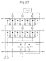
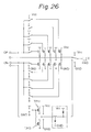
- Figure.25 illustrates a pattern diagram of an output buffer circuit as a fourth application
- Fig.26 illustrates an equivalent circuit thereof.
- FIG.27 illustrates a pattern diagram of a bidirectional buffer circuit as a fifth application
- Fig.28 illustrates an equivalent circuit thereof.
- the illustrated bidirectional buffer circuit is a combination of the input buffer circuit shown in Figs.19,20 and the output buffer circuit shown in Figs.25,26.
- the pull-up resistor or pull-down resistor can be provided with the bidirectional buffer circuit, if necessary.
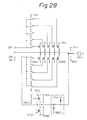
- Figure.29 illustrates a pattern diagram of a clock buffer circuit as a sixth application
- Fig.30 illustrates an equivalent circuit thereof.
- Figs.29 and 30 output signals from internal cells are fed through the terminals OP and ON, and a clock signal is fed through the terminal CI to the internal cells. Since the clock buffer circuit drives the internal cells of heavy load, its scale or size inevitably becomes large. As a result, it is difficult to constitute the clock buffer circuit by the internal cells. Contrary to this, since the clock buffer circuit according to the present embodiment is constituted by I/O cells provided in the periphery on the chip, it is possible to prevent increase in the size of the chip.
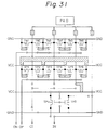
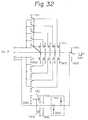
- Figure.31 illustrates a pattern diagram of a power voltage supply circuit as a seventh application
- Fig.32 illustrates an equivalent circuit thereof
- Fig.33 illustrates a pattern diagram of a ground voltage supply circuit as a eighth application
- Fig.34 illustrates an equivalent circuit thereof.
- the illustrated designing apparatus 400 comprises a fundamental mask pattern memory means 401, a wiring mask pattern memory means 402 and a pattern synthesizing means 403.
- the fundamental mask pattern memory means 401 stores two kinds of fundamental mask pattern information.
- One is a first fundamental mask pattern information consisting of four kinds of mask patterns, i.e., contact holes NA, first wiring layer(wirings) LA, through holes NB and second wiring layer(wirings) LB, necessary for forming a demanded connection between constituent elements in the basic cell region.
- Another is a second fundamental mask pattern information consisting of four kinds of mask patterns, i.e., contact holes NA, first wiring layer(wirings) LA, through holes NB and second wiring layer(wirings) LB, necessary for forming a demanded connection between constituent elements in the I/O circuits provided on the master chip.
- the wiring mask pattern memory means 402 stores two kinds of wiring mask pattern information. One is a first plurality of wiring mask patterns with respect to one wiring layer to be combined on the fundamental mask patterns, and another is a second plurality of wiring mask patterns necessary for forming one wiring layer in the program points in accordance with the kind of the I/O circuit to constitute the connection portions.
- the I/O circuit corresponds to the input buffer circuit, output buffer circuit, bidirectional buffer circuit, power voltage supply circuit or the like, as shown in Figs.19 ⁇ 34.
- the mask pattern of the internal circuit (basic cells) in the LSI is generated based on the first fundamental mask pattern information stored in the fundamental mask pattern memory means 401 and the first wiring mask pattern information stored in the wiring mask pattern memory means 402.
- the mask pattern of the I/O circuit in the LSI is generated based on the second fundamental mask pattern information and the second wiring mask pattern information.
- the second fundamental mask pattern information and the second wiring mask pattern information corresponding to the kind of the I/O circuit are read out by the pattern synthesizing means 403, where both groups of pattern information are synthesized to generate the mask pattern 404 of the I/O circuit.
- the method of producing the master slice type LSI device roughly classifying, includes the steps of forming the basic cell regions 201 together with the I/O cell regions 202 (see Fig.1) and forming the wiring pattern using a custom mask on the cell regions.
- the basic cell regions and I/O cell regions are produced by: forming an insulation layer 301 consisting of silicon oxide and including contact holes NA (not shown) on a semiconductor substrate 300; forming thereon the first wiring layer LA by aluminum(Al) evaporation; forming thereon an insulation layer 302 consisting of silicon oxide; forming through holes NB in the insulation layer 302 so that they contact the first wiring layer LA; and forming thereon a conduction layer 303.
- the mask pattern (including the mask pattern 404 of the I/O circuit) is designed by the designing apparatus 400 (see Fig.35) in accordance with the user's specification and then a desired wiring patterning is effected on the conduction layer 303 by etching process using the designed mask pattern (see Fig.36B).
- a desired second wiring layer LB is formed as shown in Fig.36C, and the master slice type LSI device according to the user's specification can be produced.
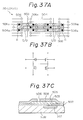
- Figures.37A to 37C illustrate a detailed plan view of the basic cell 204(205), an equivalent circuit and a sectional structure thereof, respectively.
- the basic cell is indicated by a hatched portion.
- a diffusion layer 501 of a MOS transistor formed on a substrate SUB is connected via a contact hole 503 formed in an insulation layer 502 to a first wiring layer 508.
- the first wiring layer 508 is insulated by an insulation layer 505, which includes a through hole 506 at a predetermined position.
- a through hole 506 (except for a through hole 506a) formed outside the basic cell cannot be connected to the first wiring layer(wirings) 508 connected to the diffusion layer 501 of the MOS transistor formed inside the basic cell. Accordingly, even if a second wiring layer is formed on the through hole 506, it is not short-circuited to the first wiring layer 508.
- a through hole 506 formed inside the basic cell and the above through hole 506a formed outside the basic cell constitutes a wiring obstruction pattern, where a connection between them is unnecessary.
- a wiring pattern which bypasses the wiring obstruction pattern needs to be employed.
- other region such as the bypass wiring region 240 (see Fig.15A) has been used for bypassing the wiring obstruction pattern. This is because, in the existing designing apparatus, it has been difficult to utilize an unused region on the basic cell region and design a wiring pattern for bypassing the wiring obstruction pattern, in the efficiency and speed of processing.
- bypass private region must be secured between basic cells.
- one custom mask approach cannot be utilized.
- the wiring must be formed via the bypass private region. Accordingly, there occurs another problem in that the wiring is unnecessarily lengthened and its resistance is increased.
- Figure.38 illustrates a pattern diagram of a detailed arrangement of the basic cells shown in Fig. 15A
- Fig.39 illustrates an example of connection in the bypass wiring regions 240 shown in Fig.38.
- the diffusion layer of MOS transistors formed in each basic cell 204,205 is connected via contact holes 503 to the first wiring layer(wirings)508.
- the first wiring layer(wirings)508 is connected via through holes 506 to the second wiring layer(wirings)507 formed according to the one custom mask approach.
- Figures.40A to 40H illustrate various patterns of a wiring cell, corresponding to the pattern of the basic cell 204,205 shown in Fig.37A.
- the through hole 506 formed inside the basic cell and the through hole 506a formed outside the basic cell constitutes a wiring obstruction pattern, where a connection between them is unnecessary.
- each pattern of the wiring cell 510a to 510h shown in Figs.40A to 40H is formed so as to bypass the wiring obstruction pattern.
- the wiring cell 510a shown in Fig.40A is used for connecting a through hole 506b provided at the left end of the basic cell 204 (205) to another through hole 506b provided at the right end thereof.
- the wiring cell 510b shown in Fig.40B is used for connecting each through hole 506b provided at the left and right ends of the basic cell 204 (205) to the first wiring layer(wirings) provided in the upper side thereof and connecting the first wiring layer(wirings) provided in the upper side thereof to the first wiring layer(wirings) provided in the lower side thereof.
- the wiring cell 510c shown in Fig.40C is used for connecting the first wiring layer(wirings) provided in the upper side thereof to the first wiring layer(wirings) provided in the lower side thereof.
- the wiring cell 510d shown in Fig.40D is used for connecting the through hole 506b provided at the left end thereof to the first wiring layer(wirings) provided in the lower side thereof, connecting the through hole 506b provided at the right end thereof to the first wiring layer(wirings) provided in the upper side thereof and connecting the first wiring layer(wirings) provided in the upper side thereof to the first wiring layer(wirings) provided in the lower side thereof.
- the wiring cells 510e to 510h shown in Figs.40E to 40H include an elemental pattern of the wiring cells 510a to 510d, respectively.
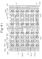
- Figure.41 illustrates a wiring pattern of an example using each wiring cell shown in Figs.40A to 40H in the basic cell region.
- the second wiring layer(wirings)507 is formed according to the one custom mask approach and constituted by a suitable combination of the wiring cells 510a to 510h.
- the pattern between points A-A′ is a combination of two wiring cells 510a
- the pattern between points B-B′ is a combination of a cell symmetrical to the wiring cell 510f with respect to X-axis, the wiring cell 510g, a cell symmetrical to the wiring cell 510f with respect to Y-axis, and the wiring cell 510a, from the left.
- the designing apparatus 400 employed in the third aspect is different from that employed in the second aspect in that a wiring cell mask pattern memory means 402a is provided in place of the wiring mask pattern memory means 402, and the mask pattern 404a of the basic cell region is generated in place of the mask pattern 404 of the I/O cell region.
- Other constitution and the operation thereof are the same as those in the second aspect and, accordingly, the explanation thereof is omitted.
- the wiring cell mask pattern memory means 402a stores a plurality of wiring cell mask pattern information concerning each pattern of the wiring cell 510a to 510h shown in Figs.40A to 40H.
- the fundamental mask pattern memory means 401 stores a fundamental mask pattern information concerning the basic cell array 206 shown in Fig.39.
- the pattern synthesizing means 403 reads out a wiring cell mask pattern information having the shortest length for bypassing the wiring obstruction pattern, from among the plurality of wiring cell mask pattern information stored in the wiring cell mask pattern memory means 402a.
- the read out wiring cell mask pattern information is combined with the fundamental mask pattern information by the pattern synthesizing means 403, which generates the wiring mask pattern 404 of the basic cell array (region).
- the designing of the wiring mask pattern of the basic cell region can be facilitated and, accordingly, it is possible to greatly reduce time needed for the designing. Accordingly, it is possible to form the wiring in the basic cell region using one custom mask approach and, accordingly, to greatly reduce time necessary for producing the master slice type LSI device. Also, since the length of the wiring to be formed is restricted to a minimum length, the wiring resistance can be decreased.
- the method of producing the master slice type LSI device with relation to the third aspect of the present invention is the same as that in the second aspect thereof and, accordingly, the explanation thereof is omitted.
Landscapes
- Engineering & Computer Science (AREA)
- Power Engineering (AREA)
- Physics & Mathematics (AREA)
- Condensed Matter Physics & Semiconductors (AREA)
- General Physics & Mathematics (AREA)
- Computer Hardware Design (AREA)
- Microelectronics & Electronic Packaging (AREA)
- Manufacturing & Machinery (AREA)
- Geometry (AREA)
- Design And Manufacture Of Integrated Circuits (AREA)
- Semiconductor Integrated Circuits (AREA)
Priority Applications (1)
| Application Number | Priority Date | Filing Date | Title |
|---|---|---|---|
| EP94119969A EP0650196A2 (de) | 1988-04-22 | 1989-04-20 | Integrierte Halbleiterschaltungsanordnung vom Masterslice-Typ und Herstellungsverfahren dafür |
Applications Claiming Priority (9)
| Application Number | Priority Date | Filing Date | Title |
|---|---|---|---|
| JP10063188 | 1988-04-22 | ||
| JP100631/88 | 1988-04-22 | ||
| JP63100631A JP2526269B2 (ja) | 1988-04-22 | 1988-04-22 | マスタスライス方法 |
| JP63180954A JPH0230164A (ja) | 1988-07-20 | 1988-07-20 | マスタスライス型半導体集積回路装置およびその製造方法 |
| JP180954/88 | 1988-07-20 | ||
| JP180953/88 | 1988-07-20 | ||
| JP18095488 | 1988-07-20 | ||
| JP18095388 | 1988-07-20 | ||
| JP63180953A JPH0230163A (ja) | 1988-07-20 | 1988-07-20 | マスタスライス型半導体集積回路装置およびその製造方法 |
Related Child Applications (2)
| Application Number | Title | Priority Date | Filing Date |
|---|---|---|---|
| EP94119969A Division EP0650196A2 (de) | 1988-04-22 | 1989-04-20 | Integrierte Halbleiterschaltungsanordnung vom Masterslice-Typ und Herstellungsverfahren dafür |
| EP94119969.7 Division-Into | 1989-04-20 |
Publications (3)
| Publication Number | Publication Date |
|---|---|
| EP0338817A2 true EP0338817A2 (de) | 1989-10-25 |
| EP0338817A3 EP0338817A3 (de) | 1992-05-06 |
| EP0338817B1 EP0338817B1 (de) | 1999-09-08 |
Family
ID=27309268
Family Applications (2)
| Application Number | Title | Priority Date | Filing Date |
|---|---|---|---|
| EP94119969A Withdrawn EP0650196A2 (de) | 1988-04-22 | 1989-04-20 | Integrierte Halbleiterschaltungsanordnung vom Masterslice-Typ und Herstellungsverfahren dafür |
| EP89303912A Expired - Lifetime EP0338817B1 (de) | 1988-04-22 | 1989-04-20 | Integrierte Halbleiterschaltungsanordnung vom "Masterslice"-Typ |
Family Applications Before (1)
| Application Number | Title | Priority Date | Filing Date |
|---|---|---|---|
| EP94119969A Withdrawn EP0650196A2 (de) | 1988-04-22 | 1989-04-20 | Integrierte Halbleiterschaltungsanordnung vom Masterslice-Typ und Herstellungsverfahren dafür |
Country Status (4)
| Country | Link |
|---|---|
| US (1) | US5506162A (de) |
| EP (2) | EP0650196A2 (de) |
| KR (1) | KR920008419B1 (de) |
| DE (1) | DE68929068T2 (de) |
Cited By (2)
| Publication number | Priority date | Publication date | Assignee | Title |
|---|---|---|---|---|
| US5252507A (en) * | 1990-03-30 | 1993-10-12 | Tactical Fabs, Inc. | Very high density wafer scale device architecture |
| US5315130A (en) * | 1990-03-30 | 1994-05-24 | Tactical Fabs, Inc. | Very high density wafer scale device architecture |
Families Citing this family (7)
| Publication number | Priority date | Publication date | Assignee | Title |
|---|---|---|---|---|
| US5691218A (en) * | 1993-07-01 | 1997-11-25 | Lsi Logic Corporation | Method of fabricating a programmable polysilicon gate array base cell structure |
| US6242767B1 (en) | 1997-11-10 | 2001-06-05 | Lightspeed Semiconductor Corp. | Asic routing architecture |
| KR100313280B1 (ko) | 1999-10-25 | 2001-11-07 | 한신혁 | 반도체 장치의 전도배선 마스크 제조방법 |
| US6613611B1 (en) | 2000-12-22 | 2003-09-02 | Lightspeed Semiconductor Corporation | ASIC routing architecture with variable number of custom masks |
| US6885043B2 (en) * | 2002-01-18 | 2005-04-26 | Lightspeed Semiconductor Corporation | ASIC routing architecture |
| JP2006156929A (ja) * | 2004-04-19 | 2006-06-15 | Fujitsu Ltd | 半導体集積回路及びその設計方法 |
| US8097918B2 (en) * | 2009-08-14 | 2012-01-17 | Infineon Technologies Ag | Semiconductor arrangement including a load transistor and sense transistor |
Citations (7)
| Publication number | Priority date | Publication date | Assignee | Title |
|---|---|---|---|---|
| FR2508255A1 (fr) * | 1981-06-22 | 1982-12-24 | Hitachi Ltd | Dispositif a circuit integre, realise a partir d'une matrice " standard, realisant une multiplicite de fonctions logiques par modification du reseau de calibrage " |
| DE3238311A1 (de) * | 1982-10-15 | 1984-04-19 | Siemens AG, 1000 Berlin und 8000 München | Integrierte halbleiterschaltung in gate-array-technik |
| GB2137413A (en) * | 1983-03-11 | 1984-10-03 | Rca Corp | Variable geometry automated universal array |
| JPS59204254A (ja) * | 1983-05-06 | 1984-11-19 | Sumitomo Electric Ind Ltd | 多層配線マスタスライスicの製造方法 |
| JPS60242639A (ja) * | 1985-03-25 | 1985-12-02 | Fujitsu Ltd | 半導体集積回路装置 |
| JPS6130050A (ja) * | 1984-07-20 | 1986-02-12 | Nec Corp | 集積論理回路装置 |
| EP0314376A1 (de) * | 1987-10-22 | 1989-05-03 | Matsushita Electronics Corporation | Integriertes Schaltkreis-Bauelement vom Typ "Master Slice" und dessen Verwendung |
Family Cites Families (20)
| Publication number | Priority date | Publication date | Assignee | Title |
|---|---|---|---|---|
| US3835530A (en) * | 1967-06-05 | 1974-09-17 | Texas Instruments Inc | Method of making semiconductor devices |
| US3702025A (en) * | 1969-05-12 | 1972-11-07 | Honeywell Inc | Discretionary interconnection process |
| US3861023A (en) * | 1973-04-30 | 1975-01-21 | Hughes Aircraft Co | Fully repairable integrated circuit interconnections |
| JPS57133712A (en) * | 1981-02-12 | 1982-08-18 | Fujitsu Ltd | Constituting method of delay circuit in master slice ic |
| EP0074805B2 (de) * | 1981-09-10 | 1992-03-11 | Fujitsu Limited | Integrierte Halbleiterschaltung mit einem Halbleitersubstrat und Verbindungsschichten |
| JPS5851537A (ja) * | 1981-09-24 | 1983-03-26 | Ricoh Co Ltd | マスタスライスチツプ |
| JPS5851538A (ja) * | 1981-09-24 | 1983-03-26 | Hitachi Ltd | 半導体集積回路装置 |
| JPS58200570A (ja) * | 1982-05-19 | 1983-11-22 | Hitachi Ltd | 半導体集積回路装置 |
| GB2122809B (en) * | 1982-06-01 | 1985-10-02 | Standard Telephones Cables Ltd | Integrated circuit interconnection bus structure |
| JPS59220940A (ja) * | 1983-05-31 | 1984-12-12 | Toshiba Corp | 電子ビ−ムによる半導体装置の内部動作電圧波形の測定方法 |
| US4617193A (en) * | 1983-06-16 | 1986-10-14 | Digital Equipment Corporation | Planar interconnect for integrated circuits |
| JPS6022337A (ja) * | 1983-07-19 | 1985-02-04 | Toshiba Corp | 半導体集積回路 |
| JPS6065547A (ja) * | 1983-09-20 | 1985-04-15 | Sharp Corp | 半導体装置 |
| JPH0828480B2 (ja) * | 1983-09-30 | 1996-03-21 | 富士通株式会社 | 半導体集積回路装置 |
| JPS60144956A (ja) * | 1984-01-06 | 1985-07-31 | Oki Electric Ind Co Ltd | 半導体装置の製造方法 |
| US4613941A (en) * | 1985-07-02 | 1986-09-23 | The United States Of America As Represented By The Secretary Of The Army | Routing method in computer aided customization of a two level automated universal array |
| DE3718598A1 (de) * | 1986-06-04 | 1987-12-10 | Mitsubishi Electric Corp | Halbleiteranordnung |
| JPS63275138A (ja) * | 1987-05-06 | 1988-11-11 | Nec Corp | 集積回路 |
| US5185283A (en) * | 1987-10-22 | 1993-02-09 | Matsushita Electronics Corporation | Method of making master slice type integrated circuit device |
| JPH02247943A (ja) * | 1989-03-20 | 1990-10-03 | Toshiba Corp | カラー受像管用シャドウマスクの洗浄方法 |
-
1989
- 1989-04-20 EP EP94119969A patent/EP0650196A2/de not_active Withdrawn
- 1989-04-20 DE DE68929068T patent/DE68929068T2/de not_active Expired - Fee Related
- 1989-04-20 EP EP89303912A patent/EP0338817B1/de not_active Expired - Lifetime
- 1989-04-22 KR KR1019890005315A patent/KR920008419B1/ko not_active IP Right Cessation
-
1995
- 1995-05-15 US US08/441,011 patent/US5506162A/en not_active Expired - Fee Related
Patent Citations (7)
| Publication number | Priority date | Publication date | Assignee | Title |
|---|---|---|---|---|
| FR2508255A1 (fr) * | 1981-06-22 | 1982-12-24 | Hitachi Ltd | Dispositif a circuit integre, realise a partir d'une matrice " standard, realisant une multiplicite de fonctions logiques par modification du reseau de calibrage " |
| DE3238311A1 (de) * | 1982-10-15 | 1984-04-19 | Siemens AG, 1000 Berlin und 8000 München | Integrierte halbleiterschaltung in gate-array-technik |
| GB2137413A (en) * | 1983-03-11 | 1984-10-03 | Rca Corp | Variable geometry automated universal array |
| JPS59204254A (ja) * | 1983-05-06 | 1984-11-19 | Sumitomo Electric Ind Ltd | 多層配線マスタスライスicの製造方法 |
| JPS6130050A (ja) * | 1984-07-20 | 1986-02-12 | Nec Corp | 集積論理回路装置 |
| JPS60242639A (ja) * | 1985-03-25 | 1985-12-02 | Fujitsu Ltd | 半導体集積回路装置 |
| EP0314376A1 (de) * | 1987-10-22 | 1989-05-03 | Matsushita Electronics Corporation | Integriertes Schaltkreis-Bauelement vom Typ "Master Slice" und dessen Verwendung |
Non-Patent Citations (3)
| Title |
|---|
| PATENT ABSTRACTS OF JAPAN vol. 10, no. 104 (E-397)(2161) 19 April 1986 & JP-A-60 242 639 ( FUJITSU LTD. ) 2 December 1985 * |
| PATENT ABSTRACTS OF JAPAN vol. 10, no. 184 (E-415)(2240) 27 June 1986 & JP-A-61 030 050 ( NEC CORP ) 12 February 1986 * |
| PATENT ABSTRACTS OF JAPAN vol. 9, no. 65 (E-304)(1788) 26 March 1985 & JP-A-59 204 254 ( SUMITOMO DENKI KOGYO K.K. ) 19 November 1984 * |
Cited By (3)
| Publication number | Priority date | Publication date | Assignee | Title |
|---|---|---|---|---|
| US5252507A (en) * | 1990-03-30 | 1993-10-12 | Tactical Fabs, Inc. | Very high density wafer scale device architecture |
| US5315130A (en) * | 1990-03-30 | 1994-05-24 | Tactical Fabs, Inc. | Very high density wafer scale device architecture |
| US5514884A (en) * | 1990-03-30 | 1996-05-07 | Tactical Fabs, Inc. | Very high density wafer scale device architecture |
Also Published As
| Publication number | Publication date |
|---|---|
| EP0650196A2 (de) | 1995-04-26 |
| KR890016667A (ko) | 1989-11-29 |
| EP0338817A3 (de) | 1992-05-06 |
| EP0650196A3 (de) | 1995-05-10 |
| EP0338817B1 (de) | 1999-09-08 |
| DE68929068D1 (de) | 1999-10-14 |
| DE68929068T2 (de) | 1999-12-23 |
| US5506162A (en) | 1996-04-09 |
| KR920008419B1 (ko) | 1992-09-28 |
Similar Documents
| Publication | Publication Date | Title |
|---|---|---|
| US4161662A (en) | Standardized digital logic chip | |
| US5079614A (en) | Gate array architecture with basic cell interleaved gate electrodes | |
| US6271548B1 (en) | Master slice LSI and layout method for the same | |
| US4668972A (en) | Masterslice semiconductor device | |
| KR920008396B1 (ko) | 반도체 집적회로 장치 | |
| US5401989A (en) | Semiconductor device having a basic cell region and an I/O cell region defined on a surface thereof | |
| US6683335B2 (en) | Gate array layout for interconnect | |
| US5760428A (en) | Variable width low profile gate array input/output architecture | |
| EP0338817A2 (de) | Integrierte Halbleiterschaltungsanordnung vom "Masterslice"-Typ und Herstellungsverfahren dafür | |
| US4750027A (en) | Master slice semiconductor device | |
| US4992845A (en) | Semiconductor integrated circuit device having input/output buffer cells each comprising a plurality of transistor regions arranged in a single line | |
| JPS58182242A (ja) | 半導体集積回路装置 | |
| US5206184A (en) | Method of making single layer personalization | |
| US5162893A (en) | Semiconductor integrated circuit device with an enlarged internal logic circuit area | |
| US8178904B2 (en) | Gate array | |
| EP0154346B1 (de) | Integrierte Halbleiterschaltungsvorrichtung | |
| EP0221431A2 (de) | Ausgerichtete Verbindungen zwischen logischen Stufen | |
| US5081059A (en) | Method of forming semiconductor integrated circuit using master slice approach | |
| JPS586157A (ja) | Cmosマスタ・スライスlsi | |
| JP2540222B2 (ja) | 集積回路 | |
| EP0662716A2 (de) | Verbesserungen in oder in bezug auf Gate-Array Zellen | |
| EP0344055B1 (de) | Integrierte Halbleiterschaltungsanordnung | |
| JP2000223575A (ja) | 半導体装置の設計方法、半導体装置および半導体装置の製造方法 | |
| US5977573A (en) | Wiring pattern for a semiconductor integrated circuit device | |
| JP3030778B2 (ja) | セミカスタム集積回路装置 |
Legal Events
| Date | Code | Title | Description |
|---|---|---|---|
| PUAI | Public reference made under article 153(3) epc to a published international application that has entered the european phase |
Free format text: ORIGINAL CODE: 0009012 |
|
| AK | Designated contracting states |
Kind code of ref document: A2 Designated state(s): DE FR GB |
|
| PUAL | Search report despatched |
Free format text: ORIGINAL CODE: 0009013 |
|
| AK | Designated contracting states |
Kind code of ref document: A3 Designated state(s): DE FR GB |
|
| 17P | Request for examination filed |
Effective date: 19920626 |
|
| 17Q | First examination report despatched |
Effective date: 19940419 |
|
| GRAG | Despatch of communication of intention to grant |
Free format text: ORIGINAL CODE: EPIDOS AGRA |
|
| GRAG | Despatch of communication of intention to grant |
Free format text: ORIGINAL CODE: EPIDOS AGRA |
|
| GRAH | Despatch of communication of intention to grant a patent |
Free format text: ORIGINAL CODE: EPIDOS IGRA |
|
| RBV | Designated contracting states (corrected) | ||
| GRAH | Despatch of communication of intention to grant a patent |
Free format text: ORIGINAL CODE: EPIDOS IGRA |
|
| GRAA | (expected) grant |
Free format text: ORIGINAL CODE: 0009210 |
|
| AK | Designated contracting states |
Kind code of ref document: B1 Designated state(s): DE FR |
|
| DX | Miscellaneous (deleted) | ||
| REF | Corresponds to: |
Ref document number: 68929068 Country of ref document: DE Date of ref document: 19991014 |
|
| ET | Fr: translation filed | ||
| PLBE | No opposition filed within time limit |
Free format text: ORIGINAL CODE: 0009261 |
|
| STAA | Information on the status of an ep patent application or granted ep patent |
Free format text: STATUS: NO OPPOSITION FILED WITHIN TIME LIMIT |
|
| 26N | No opposition filed | ||
| PGFP | Annual fee paid to national office [announced via postgrant information from national office to epo] |
Ref country code: FR Payment date: 20030408 Year of fee payment: 15 |
|
| PGFP | Annual fee paid to national office [announced via postgrant information from national office to epo] |
Ref country code: DE Payment date: 20030502 Year of fee payment: 15 |
|
| PG25 | Lapsed in a contracting state [announced via postgrant information from national office to epo] |
Ref country code: DE Free format text: LAPSE BECAUSE OF NON-PAYMENT OF DUE FEES Effective date: 20041103 |
|
| PG25 | Lapsed in a contracting state [announced via postgrant information from national office to epo] |
Ref country code: FR Free format text: LAPSE BECAUSE OF NON-PAYMENT OF DUE FEES Effective date: 20041231 |
|
| REG | Reference to a national code |
Ref country code: FR Ref legal event code: ST |