EP0293851B1 - Processeur de traitement numérique de signaux - Google Patents
Processeur de traitement numérique de signaux Download PDFInfo
- Publication number
- EP0293851B1 EP0293851B1 EP88108755A EP88108755A EP0293851B1 EP 0293851 B1 EP0293851 B1 EP 0293851B1 EP 88108755 A EP88108755 A EP 88108755A EP 88108755 A EP88108755 A EP 88108755A EP 0293851 B1 EP0293851 B1 EP 0293851B1
- Authority
- EP
- European Patent Office
- Prior art keywords
- data
- address
- memory
- microinstruction
- unit
- Prior art date
- Legal status (The legal status is an assumption and is not a legal conclusion. Google has not performed a legal analysis and makes no representation as to the accuracy of the status listed.)
- Expired - Lifetime
Links
- 230000015654 memory Effects 0.000 claims description 164
- 238000012546 transfer Methods 0.000 claims description 37
- 238000000034 method Methods 0.000 claims description 32
- 238000012545 processing Methods 0.000 claims description 22
- 238000009825 accumulation Methods 0.000 claims description 20
- 238000012360 testing method Methods 0.000 claims description 12
- 230000006870 function Effects 0.000 claims description 10
- 238000004891 communication Methods 0.000 claims description 6
- 238000006073 displacement reaction Methods 0.000 claims description 4
- 230000001174 ascending effect Effects 0.000 claims description 2
- 230000001360 synchronised effect Effects 0.000 claims 1
- 239000013598 vector Substances 0.000 description 25
- 238000010586 diagram Methods 0.000 description 8
- 230000001276 controlling effect Effects 0.000 description 7
- 238000004364 calculation method Methods 0.000 description 6
- 230000003111 delayed effect Effects 0.000 description 6
- 101100268670 Caenorhabditis elegans acc-3 gene Proteins 0.000 description 5
- 101000822152 Petunia hybrida 1-aminocyclopropane-1-carboxylate oxidase 1 Proteins 0.000 description 5
- 238000010276 construction Methods 0.000 description 5
- 238000011156 evaluation Methods 0.000 description 5
- 238000006243 chemical reaction Methods 0.000 description 3
- 230000014509 gene expression Effects 0.000 description 3
- 101000912352 Homo sapiens Putative uncharacterized protein DANCR Proteins 0.000 description 2
- 102100026242 Putative uncharacterized protein DANCR Human genes 0.000 description 2
- 238000010606 normalization Methods 0.000 description 2
- 238000013519 translation Methods 0.000 description 2
- 238000004148 unit process Methods 0.000 description 2
- 229930091051 Arenine Natural products 0.000 description 1
- 101100491817 Caenorhabditis elegans evl-20 gene Proteins 0.000 description 1
- 230000003044 adaptive effect Effects 0.000 description 1
- 101150065510 adsl-1 gene Proteins 0.000 description 1
- 229910002056 binary alloy Inorganic materials 0.000 description 1
- 230000001419 dependent effect Effects 0.000 description 1
- 230000002542 deteriorative effect Effects 0.000 description 1
- 230000009977 dual effect Effects 0.000 description 1
- 230000000694 effects Effects 0.000 description 1
- 238000001914 filtration Methods 0.000 description 1
- 238000012856 packing Methods 0.000 description 1
- 230000001105 regulatory effect Effects 0.000 description 1
- 239000000126 substance Substances 0.000 description 1
Images


Classifications
-
- G—PHYSICS
- G06—COMPUTING; CALCULATING OR COUNTING
- G06F—ELECTRIC DIGITAL DATA PROCESSING
- G06F7/00—Methods or arrangements for processing data by operating upon the order or content of the data handled
- G06F7/38—Methods or arrangements for performing computations using exclusively denominational number representation, e.g. using binary, ternary, decimal representation
- G06F7/48—Methods or arrangements for performing computations using exclusively denominational number representation, e.g. using binary, ternary, decimal representation using non-contact-making devices, e.g. tube, solid state device; using unspecified devices
- G06F7/57—Arithmetic logic units [ALU], i.e. arrangements or devices for performing two or more of the operations covered by groups G06F7/483 – G06F7/556 or for performing logical operations
- G06F7/575—Basic arithmetic logic units, i.e. devices selectable to perform either addition, subtraction or one of several logical operations, using, at least partially, the same circuitry
-
- G—PHYSICS
- G06—COMPUTING; CALCULATING OR COUNTING
- G06F—ELECTRIC DIGITAL DATA PROCESSING
- G06F13/00—Interconnection of, or transfer of information or other signals between, memories, input/output devices or central processing units
- G06F13/14—Handling requests for interconnection or transfer
- G06F13/20—Handling requests for interconnection or transfer for access to input/output bus
- G06F13/28—Handling requests for interconnection or transfer for access to input/output bus using burst mode transfer, e.g. direct memory access DMA, cycle steal
-
- G—PHYSICS
- G06—COMPUTING; CALCULATING OR COUNTING
- G06F—ELECTRIC DIGITAL DATA PROCESSING
- G06F15/00—Digital computers in general; Data processing equipment in general
- G06F15/76—Architectures of general purpose stored program computers
- G06F15/78—Architectures of general purpose stored program computers comprising a single central processing unit
- G06F15/7828—Architectures of general purpose stored program computers comprising a single central processing unit without memory
- G06F15/7832—Architectures of general purpose stored program computers comprising a single central processing unit without memory on one IC chip (single chip microprocessors)
-
- G—PHYSICS
- G06—COMPUTING; CALCULATING OR COUNTING
- G06F—ELECTRIC DIGITAL DATA PROCESSING
- G06F15/00—Digital computers in general; Data processing equipment in general
- G06F15/76—Architectures of general purpose stored program computers
- G06F15/78—Architectures of general purpose stored program computers comprising a single central processing unit
- G06F15/7839—Architectures of general purpose stored program computers comprising a single central processing unit with memory
- G06F15/7842—Architectures of general purpose stored program computers comprising a single central processing unit with memory on one IC chip (single chip microcontrollers)
- G06F15/786—Architectures of general purpose stored program computers comprising a single central processing unit with memory on one IC chip (single chip microcontrollers) using a single memory module
-
- G—PHYSICS
- G06—COMPUTING; CALCULATING OR COUNTING
- G06F—ELECTRIC DIGITAL DATA PROCESSING
- G06F9/00—Arrangements for program control, e.g. control units
- G06F9/06—Arrangements for program control, e.g. control units using stored programs, i.e. using an internal store of processing equipment to receive or retain programs
- G06F9/30—Arrangements for executing machine instructions, e.g. instruction decode
- G06F9/30003—Arrangements for executing specific machine instructions
- G06F9/3005—Arrangements for executing specific machine instructions to perform operations for flow control
- G06F9/30058—Conditional branch instructions
-
- G—PHYSICS
- G06—COMPUTING; CALCULATING OR COUNTING
- G06F—ELECTRIC DIGITAL DATA PROCESSING
- G06F9/00—Arrangements for program control, e.g. control units
- G06F9/06—Arrangements for program control, e.g. control units using stored programs, i.e. using an internal store of processing equipment to receive or retain programs
- G06F9/30—Arrangements for executing machine instructions, e.g. instruction decode
- G06F9/30094—Condition code generation, e.g. Carry, Zero flag
-
- G—PHYSICS
- G06—COMPUTING; CALCULATING OR COUNTING
- G06F—ELECTRIC DIGITAL DATA PROCESSING
- G06F9/00—Arrangements for program control, e.g. control units
- G06F9/06—Arrangements for program control, e.g. control units using stored programs, i.e. using an internal store of processing equipment to receive or retain programs
- G06F9/30—Arrangements for executing machine instructions, e.g. instruction decode
- G06F9/34—Addressing or accessing the instruction operand or the result ; Formation of operand address; Addressing modes
- G06F9/345—Addressing or accessing the instruction operand or the result ; Formation of operand address; Addressing modes of multiple operands or results
-
- G—PHYSICS
- G06—COMPUTING; CALCULATING OR COUNTING
- G06F—ELECTRIC DIGITAL DATA PROCESSING
- G06F9/00—Arrangements for program control, e.g. control units
- G06F9/06—Arrangements for program control, e.g. control units using stored programs, i.e. using an internal store of processing equipment to receive or retain programs
- G06F9/30—Arrangements for executing machine instructions, e.g. instruction decode
- G06F9/34—Addressing or accessing the instruction operand or the result ; Formation of operand address; Addressing modes
- G06F9/355—Indexed addressing
-
- G—PHYSICS
- G06—COMPUTING; CALCULATING OR COUNTING
- G06F—ELECTRIC DIGITAL DATA PROCESSING
- G06F9/00—Arrangements for program control, e.g. control units
- G06F9/06—Arrangements for program control, e.g. control units using stored programs, i.e. using an internal store of processing equipment to receive or retain programs
- G06F9/30—Arrangements for executing machine instructions, e.g. instruction decode
- G06F9/38—Concurrent instruction execution, e.g. pipeline or look ahead
- G06F9/3877—Concurrent instruction execution, e.g. pipeline or look ahead using a slave processor, e.g. coprocessor
-
- G—PHYSICS
- G06—COMPUTING; CALCULATING OR COUNTING
- G06F—ELECTRIC DIGITAL DATA PROCESSING
- G06F9/00—Arrangements for program control, e.g. control units
- G06F9/06—Arrangements for program control, e.g. control units using stored programs, i.e. using an internal store of processing equipment to receive or retain programs
- G06F9/30—Arrangements for executing machine instructions, e.g. instruction decode
- G06F9/38—Concurrent instruction execution, e.g. pipeline or look ahead
- G06F9/3885—Concurrent instruction execution, e.g. pipeline or look ahead using a plurality of independent parallel functional units
-
- G—PHYSICS
- G06—COMPUTING; CALCULATING OR COUNTING
- G06F—ELECTRIC DIGITAL DATA PROCESSING
- G06F2207/00—Indexing scheme relating to methods or arrangements for processing data by operating upon the order or content of the data handled
- G06F2207/38—Indexing scheme relating to groups G06F7/38 - G06F7/575
- G06F2207/3804—Details
- G06F2207/386—Special constructional features
- G06F2207/3884—Pipelining
Definitions
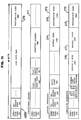
- Fig. 1 is a block diagram showing the constitution of DSSP1 (Digital Speech Signal Processor 1), namely, an exemplary conventional digital signal processor, "A High-speed VLSI Signal Processor with Normalizing Floating-point Systems", the proceedings of the annual communication Symposium of the Institute of Electronics and Communication Engineers of Japan (IECEJ), 1986, Japan.
- DSSP1 Digital Speech Signal Processor 1
- IECEJ Institute of Electronics and Communication Engineers of Japan
- the data is set in the DPO 22 and DP1 23 by the preceding microinstruction, and the contents of the P 25 is fetched by the succeeding or later microinstruction to obtain the results of multiplication. While the contents of the P 25 is being fetched, the data is held by the DPO 22, DP1 23 and the P 25. Accordingly, one multiplication operation formerly requiring three microinstructions for data input, multiplication and data output can be carried out by one microinstruction when the process is executed continuously.
- the FMPL 24 and the FALU 28 are connected by the P 25.
- the FALU is able to accumulate the contents of the P25 in the ACCO 29 to the ACC3 29 to execute one term of product-sum operation which is often used in filtering and the butterfly operation of fast Fourier transform (FFT) in one machine cycle similarly to one pair of a multiplier and accumulator shown in "Packing a signal processor onto a single digital board", Louis Schirm, Electronics, Dec. 20, 1979.
- FFT fast Fourier transform
- the product-sum is calculated by using an expression: where N is an integer not less than 1 (one), and a and hare input data.
- one term of the product-sum can be obtained for one microinstruction.
- two input data corresponding to the input data a and b must be given respectively to the DPO 22 and the DP1 23 every one microinstruction.
- the 2P-RAM 21 is enabled to supply the two input data, and a bus is provided to transfer the data read from the 20-RAM 21 directly to the DPO 22 and DP1 23 without using the D-Bus 8 to avoid bus contention in the D-Bus 8.
- the AAU 12 has output means for selectively providing two address data among address data of 9-bit width provided through the ARO 12, AR1 14 and AR2 15 mainly to address the input data of the 2P-RAM 21.
- the AAU 12 is able to specify three addresses simultaneously at the maximum only in generating addresses for the two input data given thereto from the 2P-RAM 21, and an address for one output data given through the DR 30 and the AR 20 to the external data memory.
- Each addressing is so-called indirect addressing system using an address pointer internally set in the AAU 12.
- the ARO 13 is susceptible to increment, modulo, bit reverse, repeat, increment base address and updating of increment, while the AR1 14 and the AR2 15 are susceptible only to simple increment.
- the AAU 12 is able to perform address operation only in a 9-bit natural binary system. In specifying a 12-bit address in the external data memory, three bits for specifying a memory page are added to the nine bits to specify twelve bits.
- the microinstruction execution timing of the DSSP1 will be described with reference to Fig. 2.
- the machine cycle 40 of the DSSP1 is divided into four phases of timing PO through P3.
- the nominal machine cycle time is as high as 50 nsec. Accordingly, it is practically difficult to accomplish three operations, namely, reading a microinstruction from the instruction mask ROM 2, decoding the microinstruction by the instruction decoder 5 and execution of the instruction by the internal resources such as the FMPL 24 and the FALU 28, within one machine cycle. Accordingly, the three operations are divided into stages for each machine cycle to form a three-stage pipeline to enable high-speed operation. The following operations are performed in the stages of the three-stage pipeline.
- the DSSP/1 changes the instruction succeeding the branch instruction automatically into a no-operation instruction (NOP) during the execution of the branch instruction.
- NOP no-operation instruction
- Such a function is aimed at simplifying microinstruction description, however, one machine cycle is wasted in the branching operation and two machine cycles are wasted in indirect branching operation using the D-Bus 8.
- no problem arises in about 80% of unconditional branching operations even if the succeeding instruction is executed when the sequence of instruction description is arranged properly and hence loss of machine cycles can be avoided.
- the DSSP1 is unable to avoid the loss of machine cycles.
- the DSSP1 is unable to support such an operation and hence such an operation must be decomposed into individual four arithmetic operations for processing. Therefore, three separate operations must be executed to calculate a single term.
- the process multitude can be increased by sorting in differential + square accumulation by saving interim results by the 2P-RAM 21.
- the conventional digital signal processor thus constituted has the following problems.
- the instruction memory is partly or totally reloadable, microprograms corresponding functional processes are written in the reloadable instruction memory by an external device to enable the digital signal processing to implement complex or diversified processes, and microprograms are provided automatically by an external memory when the microprograms are not written in the instruction memory.
- an external program bus 200 connecting the digital signal processor to an external extension microinstruction memory, an internal writable instruction memory (WCS) 201, a sequence control unit 202 which receives a microinstruction read through the external program bus 200 or from the WCS 201 and performs predetermined control operation in an instruction execution pipeline, an address generating unit 203 which generates 2-input 1-output addresses in parallel for data memories, three internal data buses 204 each having a width of twenty-four bits, for the parallel transfer of the 2-input 1-output data, an external bus 211 connected to an external extension data memory, an external data memory (I/F) 205 for selectively connecting one of the three internal data buses 204 to the external data bus 211, an arithmetic unit 206 which performs predetermined operations, connected to the three internal data buses 204, an internal data memory (MO) 207 having one read port and one read/write port
- the difference square sum is obtained by the delayed operation of the DPRO 226.
- this instruction is used continuously in most cases and hence problems attributable to the instruction is negligible.
- the instruction sets are classified roughly into a load 270, a branch 271, a 1-source operation 272 and a 2-source operation 273.
- a source code 274 for controlling source destination, a destination code 275, a source 0 code 276 and a source 1 code 277 are set corresponding to the function code.
- these codes are addressing codes for specifying the corresponding AGUs 256 of the address generating unit 203.
- the AGUs are identified by resource codes.
- the addressing mode can be changed over and the setting of normalization shift value can be changed for every operation instruction by using the instruction set, so that a complex signal processing algorithm can be programmed at the least loss.
Landscapes
- Engineering & Computer Science (AREA)
- Theoretical Computer Science (AREA)
- Software Systems (AREA)
- Physics & Mathematics (AREA)
- General Physics & Mathematics (AREA)
- General Engineering & Computer Science (AREA)
- Computer Hardware Design (AREA)
- Mathematical Optimization (AREA)
- Mathematical Analysis (AREA)
- Pure & Applied Mathematics (AREA)
- Computational Mathematics (AREA)
- Computing Systems (AREA)
- Microelectronics & Electronic Packaging (AREA)
- Executing Machine-Instructions (AREA)
- Advance Control (AREA)
- Complex Calculations (AREA)
Claims (13)
caractérisé par
Priority Applications (3)
| Application Number | Priority Date | Filing Date | Title |
|---|---|---|---|
| EP93104195A EP0551931B1 (fr) | 1987-06-05 | 1988-06-01 | Processeur de signaux numériques comprenant un générateur d'adresse pour accéder à des données stockées dans un espace bidirectionel d'une mémoire de données |
| EP93104196A EP0551932B1 (fr) | 1987-06-05 | 1988-06-01 | Processeur de signaux numériques opérant des branchements conditionnels multipoints en mode pipeline |
| EP93104194A EP0554917B1 (fr) | 1987-06-05 | 1988-06-01 | Système de traitement de signaux numériques comprenant un processeur accédant deux mémoires d'instruction sous contrÔle d'un ordinateur hÔte |
Applications Claiming Priority (16)
| Application Number | Priority Date | Filing Date | Title |
|---|---|---|---|
| JP14087287A JPS63304344A (ja) | 1987-06-05 | 1987-06-05 | マルチポ−トメモリ回路 |
| JP140872/87 | 1987-06-05 | ||
| JP18685887A JPS6429932A (en) | 1987-07-27 | 1987-07-27 | Address control system for signal processing |
| JP186858/87 | 1987-07-27 | ||
| JP19700987A JPS6441028A (en) | 1987-08-06 | 1987-08-06 | Interruption processing system |
| JP197009/87 | 1987-08-06 | ||
| JP273763/87 | 1987-10-29 | ||
| JP62273763A JPH0630056B2 (ja) | 1987-10-29 | 1987-10-29 | 信号処理装置 |
| JP274810/87 | 1987-10-30 | ||
| JP27481087A JPH01116730A (ja) | 1987-10-30 | 1987-10-30 | デイジタル信号処理プロセツサ |
| JP62296612A JPH0766328B2 (ja) | 1987-11-25 | 1987-11-25 | プロセッサの信号処理方式 |
| JP62296611A JPH0766327B2 (ja) | 1987-11-25 | 1987-11-25 | 信号処理方法及び装置 |
| JP296611/87 | 1987-11-25 | ||
| JP296612/87 | 1987-11-25 | ||
| JP316553/87 | 1987-12-15 | ||
| JP31655387A JPH01156825A (ja) | 1987-12-15 | 1987-12-15 | 信号処理用アドレス生成方式 |
Related Child Applications (7)
| Application Number | Title | Priority Date | Filing Date |
|---|---|---|---|
| EP93104197.4 Division-Into | 1988-06-01 | ||
| EP93104196A Division EP0551932B1 (fr) | 1987-06-05 | 1988-06-01 | Processeur de signaux numériques opérant des branchements conditionnels multipoints en mode pipeline |
| EP93104194A Division EP0554917B1 (fr) | 1987-06-05 | 1988-06-01 | Système de traitement de signaux numériques comprenant un processeur accédant deux mémoires d'instruction sous contrÔle d'un ordinateur hÔte |
| EP93104238.6 Division-Into | 1988-06-01 | ||
| EP93104194.1 Division-Into | 1988-06-01 | ||
| EP93104195A Division EP0551931B1 (fr) | 1987-06-05 | 1988-06-01 | Processeur de signaux numériques comprenant un générateur d'adresse pour accéder à des données stockées dans un espace bidirectionel d'une mémoire de données |
| EP93104196.6 Division-Into | 1988-06-01 |
Publications (3)
| Publication Number | Publication Date |
|---|---|
| EP0293851A2 EP0293851A2 (fr) | 1988-12-07 |
| EP0293851A3 EP0293851A3 (en) | 1990-05-09 |
| EP0293851B1 true EP0293851B1 (fr) | 1994-10-19 |
Family
ID=27573171
Family Applications (6)
| Application Number | Title | Priority Date | Filing Date |
|---|---|---|---|
| EP93104196A Expired - Lifetime EP0551932B1 (fr) | 1987-06-05 | 1988-06-01 | Processeur de signaux numériques opérant des branchements conditionnels multipoints en mode pipeline |
| EP93104238A Withdrawn EP0551934A2 (fr) | 1987-06-05 | 1988-06-01 | Processeur de traitement numérique |
| EP19930104197 Withdrawn EP0551933A3 (en) | 1987-06-05 | 1988-06-01 | Digital signal processor |
| EP93104195A Expired - Lifetime EP0551931B1 (fr) | 1987-06-05 | 1988-06-01 | Processeur de signaux numériques comprenant un générateur d'adresse pour accéder à des données stockées dans un espace bidirectionel d'une mémoire de données |
| EP88108755A Expired - Lifetime EP0293851B1 (fr) | 1987-06-05 | 1988-06-01 | Processeur de traitement numérique de signaux |
| EP93104194A Expired - Lifetime EP0554917B1 (fr) | 1987-06-05 | 1988-06-01 | Système de traitement de signaux numériques comprenant un processeur accédant deux mémoires d'instruction sous contrÔle d'un ordinateur hÔte |
Family Applications Before (4)
| Application Number | Title | Priority Date | Filing Date |
|---|---|---|---|
| EP93104196A Expired - Lifetime EP0551932B1 (fr) | 1987-06-05 | 1988-06-01 | Processeur de signaux numériques opérant des branchements conditionnels multipoints en mode pipeline |
| EP93104238A Withdrawn EP0551934A2 (fr) | 1987-06-05 | 1988-06-01 | Processeur de traitement numérique |
| EP19930104197 Withdrawn EP0551933A3 (en) | 1987-06-05 | 1988-06-01 | Digital signal processor |
| EP93104195A Expired - Lifetime EP0551931B1 (fr) | 1987-06-05 | 1988-06-01 | Processeur de signaux numériques comprenant un générateur d'adresse pour accéder à des données stockées dans un espace bidirectionel d'une mémoire de données |
Family Applications After (1)
| Application Number | Title | Priority Date | Filing Date |
|---|---|---|---|
| EP93104194A Expired - Lifetime EP0554917B1 (fr) | 1987-06-05 | 1988-06-01 | Système de traitement de signaux numériques comprenant un processeur accédant deux mémoires d'instruction sous contrÔle d'un ordinateur hÔte |
Country Status (4)
| Country | Link |
|---|---|
| US (1) | US5045993A (fr) |
| EP (6) | EP0551932B1 (fr) |
| CA (1) | CA1288169C (fr) |
| DE (4) | DE3851858T2 (fr) |
Families Citing this family (55)
| Publication number | Priority date | Publication date | Assignee | Title |
|---|---|---|---|---|
| CA1311063C (fr) * | 1988-12-16 | 1992-12-01 | Tokumichi Murakami | Processeur de signaux numeriques |
| JPH0769791B2 (ja) * | 1988-12-21 | 1995-07-31 | 三菱電機株式会社 | マイクロプロセッサ |
| JPH0740241B2 (ja) * | 1989-01-17 | 1995-05-01 | 富士通株式会社 | リクエストキャンセル方式 |
| US5237670A (en) * | 1989-01-30 | 1993-08-17 | Alantec, Inc. | Method and apparatus for data transfer between source and destination modules |
| US5150471A (en) * | 1989-04-20 | 1992-09-22 | Ncr Corporation | Method and apparatus for offset register address accessing |
| US5175863A (en) * | 1989-10-23 | 1992-12-29 | International Business Machines Corporation | Signal data processing system having independently, simultaneously operable alu and macu |
| EP0843254A3 (fr) * | 1990-01-18 | 1999-08-18 | National Semiconductor Corporation | Processeur de traitement de signaux numériques et processeur universal intégré avec mémoire interne partagée |
| JPH0444151A (ja) * | 1990-06-11 | 1992-02-13 | Omron Corp | プロセッサ |
| JPH0470946A (ja) * | 1990-07-04 | 1992-03-05 | Mitsubishi Electric Corp | Dmaコントローラを内蔵した処理装置 |
| JP3194193B2 (ja) * | 1990-10-31 | 2001-07-30 | カシオ計算機株式会社 | 信号処理装置 |
| RU1804645C (ru) * | 1991-03-27 | 1993-03-23 | Институт Точной Механики И Вычислительной Техники Им.С.А.Лебедева | Центральный процессор |
| US7197623B1 (en) | 1991-06-27 | 2007-03-27 | Texas Instruments Incorporated | Multiple processor cellular radio |
| FR2678400B1 (fr) * | 1991-06-27 | 1995-08-04 | Texas Instruments France | Processeur de protocole destine a l'execution d'un ensemble d'instructions en un nombre reduit d'operation. |
| JP3201786B2 (ja) * | 1991-07-18 | 2001-08-27 | アジレント・テクノロジー株式会社 | ディジタル信号処理システムの制御方法 |
| JP3172214B2 (ja) * | 1991-09-30 | 2001-06-04 | 富士通株式会社 | 状態モード設定方式 |
| JP2906792B2 (ja) * | 1991-11-15 | 1999-06-21 | 日本電気株式会社 | ディジタルプロセッサ及びその制御方法 |
| DE69228980T2 (de) * | 1991-12-06 | 1999-12-02 | Nat Semiconductor Corp | Integriertes Datenverarbeitungssystem mit CPU-Kern und unabhängigem parallelen, digitalen Signalprozessormodul |
| US6000026A (en) * | 1992-06-22 | 1999-12-07 | Texas Instrument Incorporated | Multiple processor apparatus having a protocol processor intended for the execution of a collection of instructions in a reduced number of operations |
| DE69315630T2 (de) * | 1992-07-23 | 1998-07-16 | Rockwell International Corp | Datenzugriff in einem RISC-Digitalsignalprozessor |
| WO1994006075A1 (fr) * | 1992-08-31 | 1994-03-17 | Fujitsu Limited | Procede et appareil de discrimination de caracteres non numeriques |
| US5717908A (en) * | 1993-02-25 | 1998-02-10 | Intel Corporation | Pattern recognition system using a four address arithmetic logic unit |
| US5825921A (en) * | 1993-03-19 | 1998-10-20 | Intel Corporation | Memory transfer apparatus and method useful within a pattern recognition system |
| FR2708359A1 (fr) * | 1993-06-30 | 1995-02-03 | Philips Electronics Nv | Procédé pour exploiter un processeur numérique de signal et dispositif mettant en Óoeuvre le procédé. |
| EP0638859B1 (fr) * | 1993-08-09 | 1999-09-29 | Siemens Aktiengesellschaft | Dispositif de traitement de signaux |
| JP3452655B2 (ja) * | 1993-09-27 | 2003-09-29 | 株式会社日立製作所 | ディジタル信号処理プロセッサおよびそれを用いて命令を実行する方法 |
| US5778416A (en) * | 1993-12-20 | 1998-07-07 | Motorola, Inc. | Parallel process address generator and method |
| US5590356A (en) * | 1994-08-23 | 1996-12-31 | Massachusetts Institute Of Technology | Mesh parallel computer architecture apparatus and associated methods |
| US5835730A (en) * | 1996-07-31 | 1998-11-10 | General Instrument Corporation Of Delaware | MPEG packet header compression for television modems |
| US5958048A (en) * | 1996-08-07 | 1999-09-28 | Elbrus International Ltd. | Architectural support for software pipelining of nested loops |
| WO1998006038A1 (fr) * | 1996-08-07 | 1998-02-12 | Sun Microsystems, Inc. | Support architectural pour le chevauchement de boucles par logiciel |
| WO1998006042A1 (fr) * | 1996-08-07 | 1998-02-12 | Sun Microsystems, Inc. | Procede et appareil permettant de decondenser des instructions longues |
| WO1998006041A1 (fr) * | 1996-08-07 | 1998-02-12 | Sun Microsystems, Inc. | Appareil et procede de preextraction dans un reseau |
| WO1998006039A1 (fr) * | 1996-08-07 | 1998-02-12 | Sun Microsystems, Inc. | Circuit de memoire de desambiguisation et procede de fonctionnement |
| WO1998006040A1 (fr) * | 1996-08-07 | 1998-02-12 | Sun Microsystems, Inc. | Support architectural pour le chevauchement par logiciel de boucles imbriquees |
| US5880981A (en) * | 1996-08-12 | 1999-03-09 | Hitachi America, Ltd. | Method and apparatus for reducing the power consumption in a programmable digital signal processor |
| US6332152B1 (en) * | 1997-12-02 | 2001-12-18 | Matsushita Electric Industrial Co., Ltd. | Arithmetic unit and data processing unit |
| TW380245B (en) * | 1998-05-18 | 2000-01-21 | Winbond Elelctronics Corp | Speech synthesizer and speech synthesis method |
| US7234100B1 (en) * | 2000-09-28 | 2007-06-19 | Intel Corporation | Decoder for trellis-based channel encoding |
| US6662296B1 (en) * | 2000-10-02 | 2003-12-09 | International Business Machines Corporation | Method and system for testing millicode branch points |
| JP2002215606A (ja) * | 2001-01-24 | 2002-08-02 | Mitsubishi Electric Corp | データ処理装置 |
| US20030061464A1 (en) * | 2001-06-01 | 2003-03-27 | Catherwood Michael I. | Digital signal controller instruction set and architecture |
| US20020184566A1 (en) | 2001-06-01 | 2002-12-05 | Michael Catherwood | Register pointer trap |
| US7167973B2 (en) * | 2001-11-15 | 2007-01-23 | Broadcom Corporation | Method and system for performing multi-tests in processors using results to set a register and indexing based on the register |
| JP2005149297A (ja) * | 2003-11-18 | 2005-06-09 | Renesas Technology Corp | プロセッサおよびそのアセンブラ |
| JP4908017B2 (ja) * | 2006-02-28 | 2012-04-04 | 富士通株式会社 | Dmaデータ転送装置及びdmaデータ転送方法 |
| US7953958B2 (en) * | 2006-09-29 | 2011-05-31 | Mediatek Inc. | Architecture for joint detection hardware accelerator |
| US20090129486A1 (en) * | 2007-11-15 | 2009-05-21 | Sequel Technologies, Llc. | Systems and methods for providing security communication procesess in a security system |
| GB2500707B (en) * | 2012-03-30 | 2014-09-17 | Cognovo Ltd | Multiprocessor system, apparatus and methods |
| US20150268962A1 (en) * | 2014-03-24 | 2015-09-24 | GoofyFoot Labs | Asynchronous Circuit Design |
| US9817791B2 (en) * | 2015-04-04 | 2017-11-14 | Texas Instruments Incorporated | Low energy accelerator processor architecture with short parallel instruction word |
| US11847427B2 (en) | 2015-04-04 | 2023-12-19 | Texas Instruments Incorporated | Load store circuit with dedicated single or dual bit shift circuit and opcodes for low power accelerator processor |
| US10401412B2 (en) | 2016-12-16 | 2019-09-03 | Texas Instruments Incorporated | Line fault signature analysis |
| US11010953B2 (en) * | 2017-04-21 | 2021-05-18 | Intel Corporation | Dedicated fixed point blending for energy efficiency |
| CN109714056B (zh) * | 2019-01-17 | 2022-10-28 | 上海双微导航技术有限公司 | 一种用于兼容多款ad采集的方法 |
| CN110737618B (zh) * | 2019-10-23 | 2021-03-16 | 盛科网络(苏州)有限公司 | 内嵌处理器进行快速数据通信的方法、装置及存储介质 |
Family Cites Families (19)
| Publication number | Priority date | Publication date | Assignee | Title |
|---|---|---|---|---|
| US3570006A (en) * | 1968-01-02 | 1971-03-09 | Honeywell Inc | Multiple branch technique |
| US3875391A (en) * | 1973-11-02 | 1975-04-01 | Raytheon Co | Pipeline signal processor |
| US4025771A (en) * | 1974-03-25 | 1977-05-24 | Hughes Aircraft Company | Pipe line high speed signal processor |
| US4090250A (en) * | 1976-09-30 | 1978-05-16 | Raytheon Company | Digital signal processor |
| DE2710671A1 (de) * | 1977-03-11 | 1978-09-14 | Standard Elektrik Lorenz Ag | Schaltungsanordnung fuer einen mikroprozessor zur steuerung des datenspeicherzugriffs |
| US4240139A (en) * | 1977-09-22 | 1980-12-16 | Tokyo Shibaura Denki Kabushiki Kaisha | Address generating system |
| JPS5931734B2 (ja) * | 1977-10-25 | 1984-08-03 | デイジタル イクイプメント コ−ポレ−シヨン | 特別のオペランド指定子を持つた命令を実行する中央処理装置 |
| US4159519A (en) * | 1977-11-21 | 1979-06-26 | Burroughs Corporation | Template family interfacing structure for providing a sequence of microinstructions to a pipelined microprogrammable data processing system |
| US4236206A (en) * | 1978-10-25 | 1980-11-25 | Digital Equipment Corporation | Central processor unit for executing instructions of variable length |
| US4428046A (en) * | 1980-05-05 | 1984-01-24 | Ncr Corporation | Data processing system having a star coupler with contention circuitry |
| US4493019A (en) * | 1980-05-06 | 1985-01-08 | Burroughs Corporation | Pipelined microprogrammed digital data processor employing microinstruction tasking |
| JPS5750052A (en) * | 1980-09-09 | 1982-03-24 | Toshiba Corp | Address extension system |
| US4439839A (en) * | 1981-08-24 | 1984-03-27 | International Telephone And Telegraph Corporation | Dynamically programmable processing element |
| US4654783A (en) * | 1982-07-26 | 1987-03-31 | Data General Corporation | Unique process for loading a microcode control store in a data processing system |
| JPS5979349A (ja) * | 1982-10-29 | 1984-05-08 | Toshiba Corp | 演算装置 |
| US4613935A (en) * | 1983-02-02 | 1986-09-23 | Couleur John F | Method and apparatus for pipe line processing with a single arithmetic logic unit |
| JPS59174948A (ja) * | 1983-03-25 | 1984-10-03 | Toshiba Corp | 情報処理装置 |
| US4578750A (en) * | 1983-08-24 | 1986-03-25 | Amdahl Corporation | Code determination using half-adder based operand comparator |
| US4785393A (en) * | 1984-07-09 | 1988-11-15 | Advanced Micro Devices, Inc. | 32-Bit extended function arithmetic-logic unit on a single chip |
-
1988
- 1988-06-01 EP EP93104196A patent/EP0551932B1/fr not_active Expired - Lifetime
- 1988-06-01 EP EP93104238A patent/EP0551934A2/fr not_active Withdrawn
- 1988-06-01 DE DE3851858T patent/DE3851858T2/de not_active Expired - Fee Related
- 1988-06-01 DE DE3856175T patent/DE3856175T2/de not_active Expired - Fee Related
- 1988-06-01 DE DE3856220T patent/DE3856220T2/de not_active Expired - Fee Related
- 1988-06-01 EP EP19930104197 patent/EP0551933A3/en not_active Withdrawn
- 1988-06-01 EP EP93104195A patent/EP0551931B1/fr not_active Expired - Lifetime
- 1988-06-01 EP EP88108755A patent/EP0293851B1/fr not_active Expired - Lifetime
- 1988-06-01 DE DE3856219T patent/DE3856219T2/de not_active Expired - Fee Related
- 1988-06-01 EP EP93104194A patent/EP0554917B1/fr not_active Expired - Lifetime
- 1988-06-03 CA CA000568527A patent/CA1288169C/fr not_active Expired - Fee Related
- 1988-06-03 US US07/201,208 patent/US5045993A/en not_active Expired - Fee Related
Non-Patent Citations (1)
| Title |
|---|
| Proceedings of the Annual Communication Symposium of the Institute of Electronics and Communication Engineers of Japan, 1986, pages 2-381 to 2-383 by T. Kaneko * |
Also Published As
| Publication number | Publication date |
|---|---|
| DE3856175T2 (de) | 1998-12-17 |
| EP0551934A3 (fr) | 1994-04-13 |
| EP0551932B1 (fr) | 1998-07-15 |
| US5045993A (en) | 1991-09-03 |
| EP0554917A2 (fr) | 1993-08-11 |
| EP0551933A3 (en) | 1993-12-15 |
| DE3856219D1 (de) | 1998-08-20 |
| EP0293851A3 (en) | 1990-05-09 |
| DE3856220T2 (de) | 1999-01-07 |
| EP0551932A3 (en) | 1993-12-15 |
| EP0551931A3 (en) | 1993-12-15 |
| DE3856220D1 (de) | 1998-08-20 |
| EP0551931B1 (fr) | 1998-07-15 |
| DE3856219T2 (de) | 1998-11-19 |
| EP0554917A3 (fr) | 1994-04-13 |
| CA1288169C (fr) | 1991-08-27 |
| EP0551932A2 (fr) | 1993-07-21 |
| DE3856175D1 (de) | 1998-06-10 |
| EP0554917B1 (fr) | 1998-05-06 |
| EP0551934A2 (fr) | 1993-07-21 |
| EP0551933A2 (fr) | 1993-07-21 |
| EP0293851A2 (fr) | 1988-12-07 |
| EP0551931A2 (fr) | 1993-07-21 |
| DE3851858T2 (de) | 1995-05-24 |
| DE3851858D1 (de) | 1994-11-24 |
Similar Documents
| Publication | Publication Date | Title |
|---|---|---|
| EP0293851B1 (fr) | Processeur de traitement numérique de signaux | |
| US5247627A (en) | Digital signal processor with conditional branch decision unit and storage of conditional branch decision results | |
| US5206940A (en) | Address control and generating system for digital signal-processor | |
| US5682545A (en) | Microcomputer having 16 bit fixed length instruction format | |
| US4862407A (en) | Digital signal processing apparatus | |
| US6219775B1 (en) | Massively parallel computer including auxiliary vector processor | |
| EP0127508A2 (fr) | Processeur de calcul vectoriel à virgule flottante complète | |
| CN111353126A (zh) | 分块矩阵乘法运算系统 | |
| EP1124181A1 (fr) | Appareil de traitement de données | |
| US5237667A (en) | Digital signal processor system having host processor for writing instructions into internal processor memory | |
| US5473557A (en) | Complex arithmetic processor and method | |
| US5958000A (en) | Two-bit booth multiplier with reduced data path width | |
| US5222241A (en) | Digital signal processor having duplex working registers for switching to standby state during interrupt processing | |
| JP3479385B2 (ja) | 情報処理装置 | |
| EP1122688A1 (fr) | Appareil et méthode pour le traitement de données | |
| KR19980018071A (ko) | 멀티미디어 신호 프로세서의 단일 명령 다중 데이터 처리 | |
| JPH01116730A (ja) | デイジタル信号処理プロセツサ | |
| GB2380283A (en) | A processing arrangement comprising a special purpose and a general purpose processing unit and means for supplying an instruction to cooperate to these units | |
| EP0105125A2 (fr) | Système processeur de données | |
| EP1132813A2 (fr) | Ordinateur avec changement de contexte rapide | |
| JPH07168713A (ja) | ディジタル信号処理プロセッサ | |
| EP0348030B1 (fr) | Disponibilité des résultats d'une séquence de calcul | |
| JPH07182157A (ja) | ディジタル信号処理プロセッサ | |
| JP2760808B2 (ja) | データ処理装置 | |
| JP2545798B2 (ja) | デイジタル信号処理回路 |
Legal Events
| Date | Code | Title | Description |
|---|---|---|---|
| PUAI | Public reference made under article 153(3) epc to a published international application that has entered the european phase |
Free format text: ORIGINAL CODE: 0009012 |
|
| AK | Designated contracting states |
Kind code of ref document: A2 Designated state(s): DE FR GB IT NL SE |
|
| PUAL | Search report despatched |
Free format text: ORIGINAL CODE: 0009013 |
|
| AK | Designated contracting states |
Kind code of ref document: A3 Designated state(s): DE FR GB IT NL SE |
|
| 17P | Request for examination filed |
Effective date: 19900504 |
|
| 17Q | First examination report despatched |
Effective date: 19921112 |
|
| GRAA | (expected) grant |
Free format text: ORIGINAL CODE: 0009210 |
|
| AK | Designated contracting states |
Kind code of ref document: B1 Designated state(s): DE FR GB IT NL SE |
|
| ITF | It: translation for a ep patent filed |
Owner name: ING. C. GREGORJ S.P.A. |
|
| REF | Corresponds to: |
Ref document number: 3851858 Country of ref document: DE Date of ref document: 19941124 |
|
| ET | Fr: translation filed | ||
| EAL | Se: european patent in force in sweden |
Ref document number: 88108755.5 |
|
| PGFP | Annual fee paid to national office [announced via postgrant information from national office to epo] |
Ref country code: GB Payment date: 19950522 Year of fee payment: 8 |
|
| PGFP | Annual fee paid to national office [announced via postgrant information from national office to epo] |
Ref country code: DE Payment date: 19950607 Year of fee payment: 8 |
|
| PGFP | Annual fee paid to national office [announced via postgrant information from national office to epo] |
Ref country code: FR Payment date: 19950609 Year of fee payment: 8 |
|
| PGFP | Annual fee paid to national office [announced via postgrant information from national office to epo] |
Ref country code: SE Payment date: 19950615 Year of fee payment: 8 |
|
| PGFP | Annual fee paid to national office [announced via postgrant information from national office to epo] |
Ref country code: NL Payment date: 19950628 Year of fee payment: 8 |
|
| PLBE | No opposition filed within time limit |
Free format text: ORIGINAL CODE: 0009261 |
|
| STAA | Information on the status of an ep patent application or granted ep patent |
Free format text: STATUS: NO OPPOSITION FILED WITHIN TIME LIMIT |
|
| 26N | No opposition filed | ||
| PG25 | Lapsed in a contracting state [announced via postgrant information from national office to epo] |
Ref country code: GB Effective date: 19960601 |
|
| PG25 | Lapsed in a contracting state [announced via postgrant information from national office to epo] |
Ref country code: SE Effective date: 19960602 |
|
| PG25 | Lapsed in a contracting state [announced via postgrant information from national office to epo] |
Ref country code: NL Effective date: 19970101 |
|
| GBPC | Gb: european patent ceased through non-payment of renewal fee |
Effective date: 19960601 |
|
| PG25 | Lapsed in a contracting state [announced via postgrant information from national office to epo] |
Ref country code: FR Effective date: 19970228 |
|
| PG25 | Lapsed in a contracting state [announced via postgrant information from national office to epo] |
Ref country code: DE Effective date: 19970301 |
|
| EUG | Se: european patent has lapsed |
Ref document number: 88108755.5 |
|
| NLV4 | Nl: lapsed or anulled due to non-payment of the annual fee |
Effective date: 19970101 |
|
| REG | Reference to a national code |
Ref country code: FR Ref legal event code: ST |
|
| PG25 | Lapsed in a contracting state [announced via postgrant information from national office to epo] |
Ref country code: IT Free format text: LAPSE BECAUSE OF NON-PAYMENT OF DUE FEES Effective date: 20050601 |