CN1216635A - 碳化硅上的锇整流肖特基和欧姆连接以及W/WC/TiC欧姆接触 - Google Patents
碳化硅上的锇整流肖特基和欧姆连接以及W/WC/TiC欧姆接触 Download PDFInfo
- Publication number
- CN1216635A CN1216635A CN97193978A CN97193978A CN1216635A CN 1216635 A CN1216635 A CN 1216635A CN 97193978 A CN97193978 A CN 97193978A CN 97193978 A CN97193978 A CN 97193978A CN 1216635 A CN1216635 A CN 1216635A
- Authority
- CN
- China
- Prior art keywords
- layer
- contact
- type
- sic
- substrate
- Prior art date
- Legal status (The legal status is an assumption and is not a legal conclusion. Google has not performed a legal analysis and makes no representation as to the accuracy of the status listed.)
- Pending
Links
Images


Classifications
-
- H—ELECTRICITY
- H01—ELECTRIC ELEMENTS
- H01L—SEMICONDUCTOR DEVICES NOT COVERED BY CLASS H10
- H01L24/00—Arrangements for connecting or disconnecting semiconductor or solid-state bodies; Methods or apparatus related thereto
- H01L24/01—Means for bonding being attached to, or being formed on, the surface to be connected, e.g. chip-to-package, die-attach, "first-level" interconnects; Manufacturing methods related thereto
-
- H—ELECTRICITY
- H01—ELECTRIC ELEMENTS
- H01L—SEMICONDUCTOR DEVICES NOT COVERED BY CLASS H10
- H01L21/00—Processes or apparatus adapted for the manufacture or treatment of semiconductor or solid state devices or of parts thereof
- H01L21/02—Manufacture or treatment of semiconductor devices or of parts thereof
- H01L21/04—Manufacture or treatment of semiconductor devices or of parts thereof the devices having potential barriers, e.g. a PN junction, depletion layer or carrier concentration layer
- H01L21/18—Manufacture or treatment of semiconductor devices or of parts thereof the devices having potential barriers, e.g. a PN junction, depletion layer or carrier concentration layer the devices having semiconductor bodies comprising elements of Group IV of the Periodic Table or AIIIBV compounds with or without impurities, e.g. doping materials
- H01L21/28—Manufacture of electrodes on semiconductor bodies using processes or apparatus not provided for in groups H01L21/20 - H01L21/268
- H01L21/283—Deposition of conductive or insulating materials for electrodes conducting electric current
-
- H—ELECTRICITY
- H01—ELECTRIC ELEMENTS
- H01L—SEMICONDUCTOR DEVICES NOT COVERED BY CLASS H10
- H01L21/00—Processes or apparatus adapted for the manufacture or treatment of semiconductor or solid state devices or of parts thereof
- H01L21/02—Manufacture or treatment of semiconductor devices or of parts thereof
- H01L21/04—Manufacture or treatment of semiconductor devices or of parts thereof the devices having potential barriers, e.g. a PN junction, depletion layer or carrier concentration layer
- H01L21/0445—Manufacture or treatment of semiconductor devices or of parts thereof the devices having potential barriers, e.g. a PN junction, depletion layer or carrier concentration layer the devices having semiconductor bodies comprising crystalline silicon carbide
- H01L21/048—Making electrodes
- H01L21/0485—Ohmic electrodes
-
- H—ELECTRICITY
- H01—ELECTRIC ELEMENTS
- H01L—SEMICONDUCTOR DEVICES NOT COVERED BY CLASS H10
- H01L21/00—Processes or apparatus adapted for the manufacture or treatment of semiconductor or solid state devices or of parts thereof
- H01L21/02—Manufacture or treatment of semiconductor devices or of parts thereof
- H01L21/04—Manufacture or treatment of semiconductor devices or of parts thereof the devices having potential barriers, e.g. a PN junction, depletion layer or carrier concentration layer
- H01L21/0445—Manufacture or treatment of semiconductor devices or of parts thereof the devices having potential barriers, e.g. a PN junction, depletion layer or carrier concentration layer the devices having semiconductor bodies comprising crystalline silicon carbide
- H01L21/048—Making electrodes
- H01L21/0495—Schottky electrodes
-
- H—ELECTRICITY
- H10—SEMICONDUCTOR DEVICES; ELECTRIC SOLID-STATE DEVICES NOT OTHERWISE PROVIDED FOR
- H10D—INORGANIC ELECTRIC SEMICONDUCTOR DEVICES
- H10D12/00—Bipolar devices controlled by the field effect, e.g. insulated-gate bipolar transistors [IGBT]
- H10D12/01—Manufacture or treatment
- H10D12/031—Manufacture or treatment of IGBTs
-
- H—ELECTRICITY
- H10—SEMICONDUCTOR DEVICES; ELECTRIC SOLID-STATE DEVICES NOT OTHERWISE PROVIDED FOR
- H10D—INORGANIC ELECTRIC SEMICONDUCTOR DEVICES
- H10D62/00—Semiconductor bodies, or regions thereof, of devices having potential barriers
- H10D62/80—Semiconductor bodies, or regions thereof, of devices having potential barriers characterised by the materials
- H10D62/83—Semiconductor bodies, or regions thereof, of devices having potential barriers characterised by the materials being Group IV materials, e.g. B-doped Si or undoped Ge
- H10D62/832—Semiconductor bodies, or regions thereof, of devices having potential barriers characterised by the materials being Group IV materials, e.g. B-doped Si or undoped Ge being Group IV materials comprising two or more elements, e.g. SiGe
- H10D62/8325—Silicon carbide
-
- H—ELECTRICITY
- H10—SEMICONDUCTOR DEVICES; ELECTRIC SOLID-STATE DEVICES NOT OTHERWISE PROVIDED FOR
- H10D—INORGANIC ELECTRIC SEMICONDUCTOR DEVICES
- H10D64/00—Electrodes of devices having potential barriers
- H10D64/60—Electrodes characterised by their materials
- H10D64/62—Electrodes ohmically coupled to a semiconductor
-
- H—ELECTRICITY
- H10—SEMICONDUCTOR DEVICES; ELECTRIC SOLID-STATE DEVICES NOT OTHERWISE PROVIDED FOR
- H10D—INORGANIC ELECTRIC SEMICONDUCTOR DEVICES
- H10D64/00—Electrodes of devices having potential barriers
- H10D64/60—Electrodes characterised by their materials
- H10D64/64—Electrodes comprising a Schottky barrier to a semiconductor
-
- H—ELECTRICITY
- H10—SEMICONDUCTOR DEVICES; ELECTRIC SOLID-STATE DEVICES NOT OTHERWISE PROVIDED FOR
- H10D—INORGANIC ELECTRIC SEMICONDUCTOR DEVICES
- H10D8/00—Diodes
- H10D8/01—Manufacture or treatment
- H10D8/043—Manufacture or treatment of planar diodes
-
- H—ELECTRICITY
- H10—SEMICONDUCTOR DEVICES; ELECTRIC SOLID-STATE DEVICES NOT OTHERWISE PROVIDED FOR
- H10D—INORGANIC ELECTRIC SEMICONDUCTOR DEVICES
- H10D8/00—Diodes
- H10D8/01—Manufacture or treatment
- H10D8/051—Manufacture or treatment of Schottky diodes
-
- H—ELECTRICITY
- H01—ELECTRIC ELEMENTS
- H01L—SEMICONDUCTOR DEVICES NOT COVERED BY CLASS H10
- H01L2924/00—Indexing scheme for arrangements or methods for connecting or disconnecting semiconductor or solid-state bodies as covered by H01L24/00
- H01L2924/01—Chemical elements
- H01L2924/01005—Boron [B]
-
- H—ELECTRICITY
- H01—ELECTRIC ELEMENTS
- H01L—SEMICONDUCTOR DEVICES NOT COVERED BY CLASS H10
- H01L2924/00—Indexing scheme for arrangements or methods for connecting or disconnecting semiconductor or solid-state bodies as covered by H01L24/00
- H01L2924/01—Chemical elements
- H01L2924/01006—Carbon [C]
-
- H—ELECTRICITY
- H01—ELECTRIC ELEMENTS
- H01L—SEMICONDUCTOR DEVICES NOT COVERED BY CLASS H10
- H01L2924/00—Indexing scheme for arrangements or methods for connecting or disconnecting semiconductor or solid-state bodies as covered by H01L24/00
- H01L2924/01—Chemical elements
- H01L2924/01013—Aluminum [Al]
-
- H—ELECTRICITY
- H01—ELECTRIC ELEMENTS
- H01L—SEMICONDUCTOR DEVICES NOT COVERED BY CLASS H10
- H01L2924/00—Indexing scheme for arrangements or methods for connecting or disconnecting semiconductor or solid-state bodies as covered by H01L24/00
- H01L2924/01—Chemical elements
- H01L2924/01015—Phosphorus [P]
-
- H—ELECTRICITY
- H01—ELECTRIC ELEMENTS
- H01L—SEMICONDUCTOR DEVICES NOT COVERED BY CLASS H10
- H01L2924/00—Indexing scheme for arrangements or methods for connecting or disconnecting semiconductor or solid-state bodies as covered by H01L24/00
- H01L2924/01—Chemical elements
- H01L2924/01018—Argon [Ar]
-
- H—ELECTRICITY
- H01—ELECTRIC ELEMENTS
- H01L—SEMICONDUCTOR DEVICES NOT COVERED BY CLASS H10
- H01L2924/00—Indexing scheme for arrangements or methods for connecting or disconnecting semiconductor or solid-state bodies as covered by H01L24/00
- H01L2924/01—Chemical elements
- H01L2924/01019—Potassium [K]
-
- H—ELECTRICITY
- H01—ELECTRIC ELEMENTS
- H01L—SEMICONDUCTOR DEVICES NOT COVERED BY CLASS H10
- H01L2924/00—Indexing scheme for arrangements or methods for connecting or disconnecting semiconductor or solid-state bodies as covered by H01L24/00
- H01L2924/01—Chemical elements
- H01L2924/01021—Scandium [Sc]
-
- H—ELECTRICITY
- H01—ELECTRIC ELEMENTS
- H01L—SEMICONDUCTOR DEVICES NOT COVERED BY CLASS H10
- H01L2924/00—Indexing scheme for arrangements or methods for connecting or disconnecting semiconductor or solid-state bodies as covered by H01L24/00
- H01L2924/01—Chemical elements
- H01L2924/01023—Vanadium [V]
-
- H—ELECTRICITY
- H01—ELECTRIC ELEMENTS
- H01L—SEMICONDUCTOR DEVICES NOT COVERED BY CLASS H10
- H01L2924/00—Indexing scheme for arrangements or methods for connecting or disconnecting semiconductor or solid-state bodies as covered by H01L24/00
- H01L2924/01—Chemical elements
- H01L2924/01024—Chromium [Cr]
-
- H—ELECTRICITY
- H01—ELECTRIC ELEMENTS
- H01L—SEMICONDUCTOR DEVICES NOT COVERED BY CLASS H10
- H01L2924/00—Indexing scheme for arrangements or methods for connecting or disconnecting semiconductor or solid-state bodies as covered by H01L24/00
- H01L2924/01—Chemical elements
- H01L2924/01027—Cobalt [Co]
-
- H—ELECTRICITY
- H01—ELECTRIC ELEMENTS
- H01L—SEMICONDUCTOR DEVICES NOT COVERED BY CLASS H10
- H01L2924/00—Indexing scheme for arrangements or methods for connecting or disconnecting semiconductor or solid-state bodies as covered by H01L24/00
- H01L2924/01—Chemical elements
- H01L2924/01029—Copper [Cu]
-
- H—ELECTRICITY
- H01—ELECTRIC ELEMENTS
- H01L—SEMICONDUCTOR DEVICES NOT COVERED BY CLASS H10
- H01L2924/00—Indexing scheme for arrangements or methods for connecting or disconnecting semiconductor or solid-state bodies as covered by H01L24/00
- H01L2924/01—Chemical elements
- H01L2924/0103—Zinc [Zn]
-
- H—ELECTRICITY
- H01—ELECTRIC ELEMENTS
- H01L—SEMICONDUCTOR DEVICES NOT COVERED BY CLASS H10
- H01L2924/00—Indexing scheme for arrangements or methods for connecting or disconnecting semiconductor or solid-state bodies as covered by H01L24/00
- H01L2924/01—Chemical elements
- H01L2924/01032—Germanium [Ge]
-
- H—ELECTRICITY
- H01—ELECTRIC ELEMENTS
- H01L—SEMICONDUCTOR DEVICES NOT COVERED BY CLASS H10
- H01L2924/00—Indexing scheme for arrangements or methods for connecting or disconnecting semiconductor or solid-state bodies as covered by H01L24/00
- H01L2924/01—Chemical elements
- H01L2924/01033—Arsenic [As]
-
- H—ELECTRICITY
- H01—ELECTRIC ELEMENTS
- H01L—SEMICONDUCTOR DEVICES NOT COVERED BY CLASS H10
- H01L2924/00—Indexing scheme for arrangements or methods for connecting or disconnecting semiconductor or solid-state bodies as covered by H01L24/00
- H01L2924/01—Chemical elements
- H01L2924/0104—Zirconium [Zr]
-
- H—ELECTRICITY
- H01—ELECTRIC ELEMENTS
- H01L—SEMICONDUCTOR DEVICES NOT COVERED BY CLASS H10
- H01L2924/00—Indexing scheme for arrangements or methods for connecting or disconnecting semiconductor or solid-state bodies as covered by H01L24/00
- H01L2924/01—Chemical elements
- H01L2924/01041—Niobium [Nb]
-
- H—ELECTRICITY
- H01—ELECTRIC ELEMENTS
- H01L—SEMICONDUCTOR DEVICES NOT COVERED BY CLASS H10
- H01L2924/00—Indexing scheme for arrangements or methods for connecting or disconnecting semiconductor or solid-state bodies as covered by H01L24/00
- H01L2924/01—Chemical elements
- H01L2924/01042—Molybdenum [Mo]
-
- H—ELECTRICITY
- H01—ELECTRIC ELEMENTS
- H01L—SEMICONDUCTOR DEVICES NOT COVERED BY CLASS H10
- H01L2924/00—Indexing scheme for arrangements or methods for connecting or disconnecting semiconductor or solid-state bodies as covered by H01L24/00
- H01L2924/01—Chemical elements
- H01L2924/01043—Technetium [Tc]
-
- H—ELECTRICITY
- H01—ELECTRIC ELEMENTS
- H01L—SEMICONDUCTOR DEVICES NOT COVERED BY CLASS H10
- H01L2924/00—Indexing scheme for arrangements or methods for connecting or disconnecting semiconductor or solid-state bodies as covered by H01L24/00
- H01L2924/01—Chemical elements
- H01L2924/01044—Ruthenium [Ru]
-
- H—ELECTRICITY
- H01—ELECTRIC ELEMENTS
- H01L—SEMICONDUCTOR DEVICES NOT COVERED BY CLASS H10
- H01L2924/00—Indexing scheme for arrangements or methods for connecting or disconnecting semiconductor or solid-state bodies as covered by H01L24/00
- H01L2924/01—Chemical elements
- H01L2924/01045—Rhodium [Rh]
-
- H—ELECTRICITY
- H01—ELECTRIC ELEMENTS
- H01L—SEMICONDUCTOR DEVICES NOT COVERED BY CLASS H10
- H01L2924/00—Indexing scheme for arrangements or methods for connecting or disconnecting semiconductor or solid-state bodies as covered by H01L24/00
- H01L2924/01—Chemical elements
- H01L2924/01046—Palladium [Pd]
-
- H—ELECTRICITY
- H01—ELECTRIC ELEMENTS
- H01L—SEMICONDUCTOR DEVICES NOT COVERED BY CLASS H10
- H01L2924/00—Indexing scheme for arrangements or methods for connecting or disconnecting semiconductor or solid-state bodies as covered by H01L24/00
- H01L2924/01—Chemical elements
- H01L2924/01047—Silver [Ag]
-
- H—ELECTRICITY
- H01—ELECTRIC ELEMENTS
- H01L—SEMICONDUCTOR DEVICES NOT COVERED BY CLASS H10
- H01L2924/00—Indexing scheme for arrangements or methods for connecting or disconnecting semiconductor or solid-state bodies as covered by H01L24/00
- H01L2924/01—Chemical elements
- H01L2924/01052—Tellurium [Te]
-
- H—ELECTRICITY
- H01—ELECTRIC ELEMENTS
- H01L—SEMICONDUCTOR DEVICES NOT COVERED BY CLASS H10
- H01L2924/00—Indexing scheme for arrangements or methods for connecting or disconnecting semiconductor or solid-state bodies as covered by H01L24/00
- H01L2924/01—Chemical elements
- H01L2924/01059—Praseodymium [Pr]
-
- H—ELECTRICITY
- H01—ELECTRIC ELEMENTS
- H01L—SEMICONDUCTOR DEVICES NOT COVERED BY CLASS H10
- H01L2924/00—Indexing scheme for arrangements or methods for connecting or disconnecting semiconductor or solid-state bodies as covered by H01L24/00
- H01L2924/01—Chemical elements
- H01L2924/0107—Ytterbium [Yb]
-
- H—ELECTRICITY
- H01—ELECTRIC ELEMENTS
- H01L—SEMICONDUCTOR DEVICES NOT COVERED BY CLASS H10
- H01L2924/00—Indexing scheme for arrangements or methods for connecting or disconnecting semiconductor or solid-state bodies as covered by H01L24/00
- H01L2924/01—Chemical elements
- H01L2924/01072—Hafnium [Hf]
-
- H—ELECTRICITY
- H01—ELECTRIC ELEMENTS
- H01L—SEMICONDUCTOR DEVICES NOT COVERED BY CLASS H10
- H01L2924/00—Indexing scheme for arrangements or methods for connecting or disconnecting semiconductor or solid-state bodies as covered by H01L24/00
- H01L2924/01—Chemical elements
- H01L2924/01073—Tantalum [Ta]
-
- H—ELECTRICITY
- H01—ELECTRIC ELEMENTS
- H01L—SEMICONDUCTOR DEVICES NOT COVERED BY CLASS H10
- H01L2924/00—Indexing scheme for arrangements or methods for connecting or disconnecting semiconductor or solid-state bodies as covered by H01L24/00
- H01L2924/01—Chemical elements
- H01L2924/01074—Tungsten [W]
-
- H—ELECTRICITY
- H01—ELECTRIC ELEMENTS
- H01L—SEMICONDUCTOR DEVICES NOT COVERED BY CLASS H10
- H01L2924/00—Indexing scheme for arrangements or methods for connecting or disconnecting semiconductor or solid-state bodies as covered by H01L24/00
- H01L2924/01—Chemical elements
- H01L2924/01075—Rhenium [Re]
-
- H—ELECTRICITY
- H01—ELECTRIC ELEMENTS
- H01L—SEMICONDUCTOR DEVICES NOT COVERED BY CLASS H10
- H01L2924/00—Indexing scheme for arrangements or methods for connecting or disconnecting semiconductor or solid-state bodies as covered by H01L24/00
- H01L2924/01—Chemical elements
- H01L2924/01076—Osmium [Os]
-
- H—ELECTRICITY
- H01—ELECTRIC ELEMENTS
- H01L—SEMICONDUCTOR DEVICES NOT COVERED BY CLASS H10
- H01L2924/00—Indexing scheme for arrangements or methods for connecting or disconnecting semiconductor or solid-state bodies as covered by H01L24/00
- H01L2924/01—Chemical elements
- H01L2924/01077—Iridium [Ir]
-
- H—ELECTRICITY
- H01—ELECTRIC ELEMENTS
- H01L—SEMICONDUCTOR DEVICES NOT COVERED BY CLASS H10
- H01L2924/00—Indexing scheme for arrangements or methods for connecting or disconnecting semiconductor or solid-state bodies as covered by H01L24/00
- H01L2924/01—Chemical elements
- H01L2924/01078—Platinum [Pt]
-
- H—ELECTRICITY
- H01—ELECTRIC ELEMENTS
- H01L—SEMICONDUCTOR DEVICES NOT COVERED BY CLASS H10
- H01L2924/00—Indexing scheme for arrangements or methods for connecting or disconnecting semiconductor or solid-state bodies as covered by H01L24/00
- H01L2924/01—Chemical elements
- H01L2924/01079—Gold [Au]
-
- H—ELECTRICITY
- H01—ELECTRIC ELEMENTS
- H01L—SEMICONDUCTOR DEVICES NOT COVERED BY CLASS H10
- H01L2924/00—Indexing scheme for arrangements or methods for connecting or disconnecting semiconductor or solid-state bodies as covered by H01L24/00
- H01L2924/01—Chemical elements
- H01L2924/01082—Lead [Pb]
-
- H—ELECTRICITY
- H01—ELECTRIC ELEMENTS
- H01L—SEMICONDUCTOR DEVICES NOT COVERED BY CLASS H10
- H01L2924/00—Indexing scheme for arrangements or methods for connecting or disconnecting semiconductor or solid-state bodies as covered by H01L24/00
- H01L2924/013—Alloys
- H01L2924/0132—Binary Alloys
- H01L2924/01327—Intermediate phases, i.e. intermetallics compounds
-
- H—ELECTRICITY
- H01—ELECTRIC ELEMENTS
- H01L—SEMICONDUCTOR DEVICES NOT COVERED BY CLASS H10
- H01L2924/00—Indexing scheme for arrangements or methods for connecting or disconnecting semiconductor or solid-state bodies as covered by H01L24/00
- H01L2924/10—Details of semiconductor or other solid state devices to be connected
- H01L2924/102—Material of the semiconductor or solid state bodies
- H01L2924/1025—Semiconducting materials
- H01L2924/10251—Elemental semiconductors, i.e. Group IV
- H01L2924/10253—Silicon [Si]
-
- H—ELECTRICITY
- H01—ELECTRIC ELEMENTS
- H01L—SEMICONDUCTOR DEVICES NOT COVERED BY CLASS H10
- H01L2924/00—Indexing scheme for arrangements or methods for connecting or disconnecting semiconductor or solid-state bodies as covered by H01L24/00
- H01L2924/10—Details of semiconductor or other solid state devices to be connected
- H01L2924/102—Material of the semiconductor or solid state bodies
- H01L2924/1025—Semiconducting materials
- H01L2924/1026—Compound semiconductors
- H01L2924/1027—IV
- H01L2924/10272—Silicon Carbide [SiC]
-
- H—ELECTRICITY
- H01—ELECTRIC ELEMENTS
- H01L—SEMICONDUCTOR DEVICES NOT COVERED BY CLASS H10
- H01L2924/00—Indexing scheme for arrangements or methods for connecting or disconnecting semiconductor or solid-state bodies as covered by H01L24/00
- H01L2924/10—Details of semiconductor or other solid state devices to be connected
- H01L2924/102—Material of the semiconductor or solid state bodies
- H01L2924/1025—Semiconducting materials
- H01L2924/1026—Compound semiconductors
- H01L2924/1032—III-V
- H01L2924/10329—Gallium arsenide [GaAs]
-
- H—ELECTRICITY
- H01—ELECTRIC ELEMENTS
- H01L—SEMICONDUCTOR DEVICES NOT COVERED BY CLASS H10
- H01L2924/00—Indexing scheme for arrangements or methods for connecting or disconnecting semiconductor or solid-state bodies as covered by H01L24/00
- H01L2924/10—Details of semiconductor or other solid state devices to be connected
- H01L2924/11—Device type
- H01L2924/12—Passive devices, e.g. 2 terminal devices
- H01L2924/1203—Rectifying Diode
- H01L2924/12032—Schottky diode
-
- H—ELECTRICITY
- H01—ELECTRIC ELEMENTS
- H01L—SEMICONDUCTOR DEVICES NOT COVERED BY CLASS H10
- H01L2924/00—Indexing scheme for arrangements or methods for connecting or disconnecting semiconductor or solid-state bodies as covered by H01L24/00
- H01L2924/10—Details of semiconductor or other solid state devices to be connected
- H01L2924/11—Device type
- H01L2924/12—Passive devices, e.g. 2 terminal devices
- H01L2924/1203—Rectifying Diode
- H01L2924/12036—PN diode
-
- H—ELECTRICITY
- H01—ELECTRIC ELEMENTS
- H01L—SEMICONDUCTOR DEVICES NOT COVERED BY CLASS H10
- H01L2924/00—Indexing scheme for arrangements or methods for connecting or disconnecting semiconductor or solid-state bodies as covered by H01L24/00
- H01L2924/10—Details of semiconductor or other solid state devices to be connected
- H01L2924/11—Device type
- H01L2924/13—Discrete devices, e.g. 3 terminal devices
- H01L2924/1301—Thyristor
- H01L2924/13034—Silicon Controlled Rectifier [SCR]
-
- H—ELECTRICITY
- H01—ELECTRIC ELEMENTS
- H01L—SEMICONDUCTOR DEVICES NOT COVERED BY CLASS H10
- H01L2924/00—Indexing scheme for arrangements or methods for connecting or disconnecting semiconductor or solid-state bodies as covered by H01L24/00
- H01L2924/10—Details of semiconductor or other solid state devices to be connected
- H01L2924/11—Device type
- H01L2924/13—Discrete devices, e.g. 3 terminal devices
- H01L2924/1304—Transistor
- H01L2924/1305—Bipolar Junction Transistor [BJT]
- H01L2924/13055—Insulated gate bipolar transistor [IGBT]
-
- H—ELECTRICITY
- H01—ELECTRIC ELEMENTS
- H01L—SEMICONDUCTOR DEVICES NOT COVERED BY CLASS H10
- H01L2924/00—Indexing scheme for arrangements or methods for connecting or disconnecting semiconductor or solid-state bodies as covered by H01L24/00
- H01L2924/10—Details of semiconductor or other solid state devices to be connected
- H01L2924/11—Device type
- H01L2924/13—Discrete devices, e.g. 3 terminal devices
- H01L2924/1304—Transistor
- H01L2924/1306—Field-effect transistor [FET]
- H01L2924/13063—Metal-Semiconductor Field-Effect Transistor [MESFET]
-
- H—ELECTRICITY
- H01—ELECTRIC ELEMENTS
- H01L—SEMICONDUCTOR DEVICES NOT COVERED BY CLASS H10
- H01L2924/00—Indexing scheme for arrangements or methods for connecting or disconnecting semiconductor or solid-state bodies as covered by H01L24/00
- H01L2924/10—Details of semiconductor or other solid state devices to be connected
- H01L2924/11—Device type
- H01L2924/13—Discrete devices, e.g. 3 terminal devices
- H01L2924/1304—Transistor
- H01L2924/1306—Field-effect transistor [FET]
- H01L2924/13091—Metal-Oxide-Semiconductor Field-Effect Transistor [MOSFET]
-
- H—ELECTRICITY
- H01—ELECTRIC ELEMENTS
- H01L—SEMICONDUCTOR DEVICES NOT COVERED BY CLASS H10
- H01L2924/00—Indexing scheme for arrangements or methods for connecting or disconnecting semiconductor or solid-state bodies as covered by H01L24/00
- H01L2924/10—Details of semiconductor or other solid state devices to be connected
- H01L2924/11—Device type
- H01L2924/14—Integrated circuits
-
- H—ELECTRICITY
- H01—ELECTRIC ELEMENTS
- H01L—SEMICONDUCTOR DEVICES NOT COVERED BY CLASS H10
- H01L2924/00—Indexing scheme for arrangements or methods for connecting or disconnecting semiconductor or solid-state bodies as covered by H01L24/00
- H01L2924/19—Details of hybrid assemblies other than the semiconductor or other solid state devices to be connected
- H01L2924/1901—Structure
- H01L2924/1904—Component type
- H01L2924/19043—Component type being a resistor
-
- H—ELECTRICITY
- H01—ELECTRIC ELEMENTS
- H01L—SEMICONDUCTOR DEVICES NOT COVERED BY CLASS H10
- H01L2924/00—Indexing scheme for arrangements or methods for connecting or disconnecting semiconductor or solid-state bodies as covered by H01L24/00
- H01L2924/30—Technical effects
- H01L2924/301—Electrical effects
- H01L2924/3025—Electromagnetic shielding
Landscapes
- Engineering & Computer Science (AREA)
- Power Engineering (AREA)
- Computer Hardware Design (AREA)
- Microelectronics & Electronic Packaging (AREA)
- General Physics & Mathematics (AREA)
- Physics & Mathematics (AREA)
- Manufacturing & Machinery (AREA)
- Condensed Matter Physics & Semiconductors (AREA)
- Crystallography & Structural Chemistry (AREA)
- Chemical & Material Sciences (AREA)
- Electrodes Of Semiconductors (AREA)
- Thyristors (AREA)
- Semiconductor Integrated Circuits (AREA)
- Junction Field-Effect Transistors (AREA)
- Insulated Gate Type Field-Effect Transistor (AREA)
Applications Claiming Priority (2)
| Application Number | Priority Date | Filing Date | Title |
|---|---|---|---|
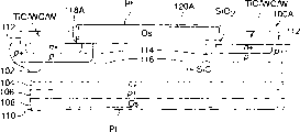
| US08/612,216 US5929523A (en) | 1996-03-07 | 1996-03-07 | Os rectifying Schottky and ohmic junction and W/WC/TiC ohmic contacts on SiC |
| US08/612,216 | 1996-03-07 |
Publications (1)
| Publication Number | Publication Date |
|---|---|
| CN1216635A true CN1216635A (zh) | 1999-05-12 |
Family
ID=24452227
Family Applications (1)
| Application Number | Title | Priority Date | Filing Date |
|---|---|---|---|
| CN97193978A Pending CN1216635A (zh) | 1996-03-07 | 1997-03-04 | 碳化硅上的锇整流肖特基和欧姆连接以及W/WC/TiC欧姆接触 |
Country Status (9)
| Country | Link |
|---|---|
| US (2) | US5929523A (cg-RX-API-DMAC7.html) |
| EP (1) | EP0944917A1 (cg-RX-API-DMAC7.html) |
| JP (1) | JP2000507043A (cg-RX-API-DMAC7.html) |
| KR (1) | KR19990087549A (cg-RX-API-DMAC7.html) |
| CN (1) | CN1216635A (cg-RX-API-DMAC7.html) |
| AU (1) | AU2069497A (cg-RX-API-DMAC7.html) |
| CA (1) | CA2248803A1 (cg-RX-API-DMAC7.html) |
| TW (1) | TW337618B (cg-RX-API-DMAC7.html) |
| WO (1) | WO1997033308A1 (cg-RX-API-DMAC7.html) |
Cited By (6)
| Publication number | Priority date | Publication date | Assignee | Title |
|---|---|---|---|---|
| CN102668040A (zh) * | 2009-10-01 | 2012-09-12 | 丰田自动车株式会社 | 半导体装置以及半导体装置的制造方法 |
| CN103208490A (zh) * | 2012-01-11 | 2013-07-17 | 朱江 | 一种具有导体的半导体装置及其制备方法 |
| CN104037075A (zh) * | 2014-06-12 | 2014-09-10 | 中国电子科技集团公司第五十五研究所 | 耐高温处理的碳化硅背面金属加厚方法 |
| CN104538294A (zh) * | 2015-01-04 | 2015-04-22 | 中国科学院半导体研究所 | 一种碳化硅欧姆接触电极及其制作方法 |
| CN104918823A (zh) * | 2013-01-15 | 2015-09-16 | 康斯博格汽车股份公司 | 具有沿着预定路径向区间提供可变温度的电加热的加热元件的座椅组件 |
| CN108807168A (zh) * | 2012-06-27 | 2018-11-13 | 飞兆半导体公司 | 功率整流器件 |
Families Citing this family (45)
| Publication number | Priority date | Publication date | Assignee | Title |
|---|---|---|---|---|
| US5929523A (en) * | 1996-03-07 | 1999-07-27 | 3C Semiconductor Corporation | Os rectifying Schottky and ohmic junction and W/WC/TiC ohmic contacts on SiC |
| US6388272B1 (en) * | 1996-03-07 | 2002-05-14 | Caldus Semiconductor, Inc. | W/WC/TAC ohmic and rectifying contacts on SiC |
| US6027954A (en) * | 1998-05-29 | 2000-02-22 | The United States Of America As Represented By The Administrator Of The National Aeronautics And Space Administration | Gas sensing diode and method of manufacturing |
| DE19925233A1 (de) * | 1998-06-08 | 1999-12-09 | Siemens Ag | Halbleiteranordnung mit ohmscher Kontaktierung und Verfahren zur Kontaktierung einer Halbleiteranordnung |
| JP3361062B2 (ja) | 1998-09-17 | 2003-01-07 | 株式会社東芝 | 半導体装置 |
| TW408411B (en) * | 1999-03-31 | 2000-10-11 | Huang Jr Gung | Semiconductor chip scale package |
| EP1222694B1 (de) * | 1999-09-22 | 2005-02-02 | SiCED Electronics Development GmbH & Co KG | SiC-Halbleitervorrichtung mit einem Schottky-Kontakt und Verfahren zu deren Herstellung |
| US6303082B1 (en) * | 1999-12-15 | 2001-10-16 | Nanogen, Inc. | Permeation layer attachment chemistry and method |
| DE10005368A1 (de) * | 2000-02-07 | 2001-08-16 | Daimler Chrysler Ag | Bildung legierter ohmscher Kontakte auf Halbleitermaterialien |
| KR20020066578A (ko) * | 2001-02-12 | 2002-08-19 | 광주과학기술원 | 질화물반도체 소자에 사용되는 오믹금속전극 제조방법 |
| JP2002122560A (ja) | 2000-08-10 | 2002-04-26 | Ngk Spark Plug Co Ltd | ガスセンサ |
| JP2002076022A (ja) * | 2000-09-01 | 2002-03-15 | New Japan Radio Co Ltd | 半導体装置 |
| US6599644B1 (en) | 2000-10-06 | 2003-07-29 | Foundation For Research & Technology-Hellas | Method of making an ohmic contact to p-type silicon carbide, comprising titanium carbide and nickel silicide |
| US7297626B1 (en) | 2001-08-27 | 2007-11-20 | United States Of America As Represented By The Secretary Of The Army | Process for nickel silicide Ohmic contacts to n-SiC |
| US6759683B1 (en) * | 2001-08-27 | 2004-07-06 | The United States Of America As Represented By The Secretary Of The Army | Formulation and fabrication of an improved Ni based composite Ohmic contact to n-SiC for high temperature and high power device applications |
| US7183575B2 (en) * | 2002-02-19 | 2007-02-27 | Nissan Motor Co., Ltd. | High reverse voltage silicon carbide diode and method of manufacturing the same high reverse voltage silicon carbide diode |
| US7262434B2 (en) | 2002-03-28 | 2007-08-28 | Rohm Co., Ltd. | Semiconductor device with a silicon carbide substrate and ohmic metal layer |
| KR100831974B1 (ko) * | 2002-07-12 | 2008-05-26 | 주식회사 하이닉스반도체 | 텅스텐을 적용한 이중 일 함수 금속 게이트 전극 및 그제조 방법 |
| US6833556B2 (en) | 2002-08-12 | 2004-12-21 | Acorn Technologies, Inc. | Insulated gate field effect transistor having passivated schottky barriers to the channel |
| US7084423B2 (en) | 2002-08-12 | 2006-08-01 | Acorn Technologies, Inc. | Method for depinning the Fermi level of a semiconductor at an electrical junction and devices incorporating such junctions |
| KR100482845B1 (ko) * | 2002-08-22 | 2005-04-14 | 한국전기연구원 | 탄화규소 백투백 쇼트키 장벽 다이오드 구조체 |
| US6974720B2 (en) * | 2003-10-16 | 2005-12-13 | Cree, Inc. | Methods of forming power semiconductor devices using boule-grown silicon carbide drift layers and power semiconductor devices formed thereby |
| US7812441B2 (en) | 2004-10-21 | 2010-10-12 | Siliconix Technology C.V. | Schottky diode with improved surge capability |
| TWI278090B (en) * | 2004-10-21 | 2007-04-01 | Int Rectifier Corp | Solderable top metal for SiC device |
| US9419092B2 (en) * | 2005-03-04 | 2016-08-16 | Vishay-Siliconix | Termination for SiC trench devices |
| US7834376B2 (en) | 2005-03-04 | 2010-11-16 | Siliconix Technology C. V. | Power semiconductor switch |
| US8368165B2 (en) | 2005-10-20 | 2013-02-05 | Siliconix Technology C. V. | Silicon carbide Schottky diode |
| DE112007000697B4 (de) * | 2006-03-22 | 2013-11-07 | Mitsubishi Electric Corp. | Leistungshalbleitervorrichtung |
| JP2009545885A (ja) * | 2006-07-31 | 2009-12-24 | ヴィシェイ−シリコニックス | SiCショットキーダイオード用モリブデンバリア金属および製造方法 |
| JP5078314B2 (ja) * | 2006-10-18 | 2012-11-21 | ローム株式会社 | ショットキーバリアダイオードおよびその製造方法 |
| JP2008235767A (ja) * | 2007-03-23 | 2008-10-02 | Univ Of Fukui | 半導体素子及びその製造方法 |
| JP5435922B2 (ja) * | 2008-08-12 | 2014-03-05 | 新電元工業株式会社 | ショットキーバリアダイオードの製造方法 |
| US7915703B2 (en) | 2009-05-13 | 2011-03-29 | Cree, Inc. | Schottky diodes containing high barrier metal islands in a low barrier metal layer and methods of forming the same |
| US9362376B2 (en) | 2011-11-23 | 2016-06-07 | Acorn Technologies, Inc. | Metal contacts to group IV semiconductors by inserting interfacial atomic monolayers |
| TWI484626B (zh) * | 2012-02-21 | 2015-05-11 | 璨圓光電股份有限公司 | 半導體發光元件及具有此半導體發光元件的發光裝置 |
| JP2015065315A (ja) * | 2013-09-25 | 2015-04-09 | 新日鐵住金株式会社 | SiC半導体デバイス及びその製造方法 |
| DE102015108703A1 (de) * | 2015-06-02 | 2016-12-08 | Infineon Technologies Ag | Verfahren zum Bilden einer Mehrzahl von Halbleiterbauelementen auf einer Mehrzahl von Halbleiterwafern |
| JP6584879B2 (ja) * | 2015-09-11 | 2019-10-02 | 株式会社東芝 | 半導体装置 |
| US10381455B1 (en) | 2015-09-11 | 2019-08-13 | United States Of America As Represented By The Administrator Of National Aeronautics And Space Administration | Diffusion barrier systems (DBS) for high temperature semiconductor electrical contacts |
| JP6584880B2 (ja) * | 2015-09-11 | 2019-10-02 | 株式会社東芝 | 半導体装置 |
| US9620611B1 (en) | 2016-06-17 | 2017-04-11 | Acorn Technology, Inc. | MIS contact structure with metal oxide conductor |
| DE112017005855T5 (de) | 2016-11-18 | 2019-08-01 | Acorn Technologies, Inc. | Nanodrahttransistor mit Source und Drain induziert durch elektrische Kontakte mit negativer Schottky-Barrierenhöhe |
| EP4008025B1 (en) | 2019-08-01 | 2023-09-06 | Hitachi Energy Switzerland AG | Silicon carbide transistor device |
| US12054845B2 (en) * | 2021-12-21 | 2024-08-06 | Battelle Energy Alliance, Llc | Metal coated articles comprising a refractory metal region and a platinum-group metal region, and related methods |
| CN115251933A (zh) * | 2022-06-20 | 2022-11-01 | Oppo广东移动通信有限公司 | 电极及其制备方法和电子设备 |
Family Cites Families (40)
| Publication number | Priority date | Publication date | Assignee | Title |
|---|---|---|---|---|
| DE1073110B (de) * | 1957-08-16 | 1960-01-14 | General Electric Company, Schenectady, N Y (V St A) | Verfahren zur Herstellung gleichrichtender oder ohmscher Anschlußkontakte an Siliziumkarbidkorpern |
| NL230892A (cg-RX-API-DMAC7.html) * | 1958-08-27 | |||
| GB1052587A (cg-RX-API-DMAC7.html) * | 1964-06-30 | |||
| US3510733A (en) * | 1966-05-13 | 1970-05-05 | Gen Electric | Semiconductive crystals of silicon carbide with improved chromium-containing electrical contacts |
| US3492719A (en) * | 1967-03-10 | 1970-02-03 | Westinghouse Electric Corp | Evaporated metal contacts for the fabrication of silicon carbide devices |
| US3611064A (en) * | 1969-07-14 | 1971-10-05 | Gen Electric | Ohmic contact to n-type silicon carbide, comprising nickel-titanium-gold |
| US3844029A (en) * | 1972-02-02 | 1974-10-29 | Trw Inc | High power double-slug diode package |
| US3831187A (en) * | 1973-04-11 | 1974-08-20 | Rca Corp | Thyristor having capacitively coupled control electrode |
| US4199774A (en) * | 1978-09-18 | 1980-04-22 | The Board Of Trustees Of The Leland Stanford Junior University | Monolithic semiconductor switching device |
| US4364073A (en) * | 1980-03-25 | 1982-12-14 | Rca Corporation | Power MOSFET with an anode region |
| JPS58223678A (ja) * | 1982-06-16 | 1983-12-26 | 株式会社日立製作所 | 金属化層を有するSiC焼結体とその製法 |
| JPH0791610B2 (ja) * | 1985-06-17 | 1995-10-04 | 日本電装株式会社 | 非酸化物セラミックヒータ用金属ロー材 |
| US4738937A (en) * | 1985-10-22 | 1988-04-19 | Hughes Aircraft Company | Method of making ohmic contact structure |
| US4782377A (en) * | 1986-09-30 | 1988-11-01 | Colorado State University Research Foundation | Semiconducting metal silicide radiation detectors and source |
| US4940898A (en) * | 1986-09-30 | 1990-07-10 | Colorado State University Research Foundation | Semiconducting metal silicide radiation detectors |
| US4914042A (en) * | 1986-09-30 | 1990-04-03 | Colorado State University Research Foundation | Forming a transition metal silicide radiation detector and source |
| JPS63278202A (ja) * | 1987-05-09 | 1988-11-15 | Oki Electric Ind Co Ltd | 発熱抵抗体 |
| US5270252A (en) * | 1988-10-25 | 1993-12-14 | United States Of America As Represented By The Secretary Of The Navy | Method of forming platinum and platinum silicide schottky contacts on beta-silicon carbide |
| US5216264A (en) * | 1989-06-07 | 1993-06-01 | Sharp Kabushiki Kaisha | Silicon carbide MOS type field-effect transistor with at least one of the source and drain regions is formed by the use of a schottky contact |
| JP2509713B2 (ja) * | 1989-10-18 | 1996-06-26 | シャープ株式会社 | 炭化珪素半導体装置およびその製造方法 |
| US5190890A (en) * | 1990-06-04 | 1993-03-02 | Advanced Technology Materials, Inc. | Wafer base for silicon carbide semiconductor devices, incorporating alloy substrates, and method of making the same |
| JPH04317374A (ja) * | 1991-04-16 | 1992-11-09 | Sanyo Electric Co Ltd | SiCデバイスの電極形成方法 |
| US5165283A (en) * | 1991-05-02 | 1992-11-24 | Kulite Semiconductor Products, Inc. | High temperature transducers and methods of fabricating the same employing silicon carbide |
| JPH05283361A (ja) * | 1992-04-03 | 1993-10-29 | Sumitomo Electric Ind Ltd | ダイヤモンド半導体装置およびその製造方法 |
| US5294814A (en) * | 1992-06-09 | 1994-03-15 | Kobe Steel Usa | Vertical diamond field effect transistor |
| US5559399A (en) * | 1992-06-11 | 1996-09-24 | Norden Systems, Inc. | Low resistance, thermally stable electrode structure for electroluminescent displays |
| US5384470A (en) * | 1992-11-02 | 1995-01-24 | Kobe Steel, Usa, Inc. | High temperature rectifying contact including polycrystalline diamond and method for making same |
| TW226478B (en) * | 1992-12-04 | 1994-07-11 | Semiconductor Energy Res Co Ltd | Semiconductor device and method for manufacturing the same |
| US5492752A (en) * | 1992-12-07 | 1996-02-20 | Oregon Graduate Institute Of Science And Technology | Substrates for the growth of 3C-silicon carbide |
| JP3086556B2 (ja) * | 1993-02-09 | 2000-09-11 | 株式会社神戸製鋼所 | 半導体ダイヤモンド層上の耐熱性オーミック電極及びその形成方法 |
| US5448081A (en) * | 1993-02-22 | 1995-09-05 | Texas Instruments Incorporated | Lateral power MOSFET structure using silicon carbide |
| US5407855A (en) * | 1993-06-07 | 1995-04-18 | Motorola, Inc. | Process for forming a semiconductor device having a reducing/oxidizing conductive material |
| US5388027A (en) * | 1993-07-29 | 1995-02-07 | Motorola, Inc. | Electronic circuit assembly with improved heatsinking |
| JP3304541B2 (ja) * | 1993-09-08 | 2002-07-22 | 住友電気工業株式会社 | オーミック電極の形成方法 |
| US5449925A (en) * | 1994-05-04 | 1995-09-12 | North Carolina State University | Voltage breakdown resistant monocrystalline silicon carbide semiconductor devices |
| US5442200A (en) * | 1994-06-03 | 1995-08-15 | Advanced Technology Materials, Inc. | Low resistance, stable ohmic contacts to silcon carbide, and method of making the same |
| KR0153878B1 (ko) * | 1994-06-07 | 1998-10-15 | 쿠미하시 요시유키 | 탄화규소반도체장치와 그 제조방법 |
| US5455432A (en) * | 1994-10-11 | 1995-10-03 | Kobe Steel Usa | Diamond semiconductor device with carbide interlayer |
| JP2995284B2 (ja) * | 1995-08-25 | 1999-12-27 | 工業技術院長 | 電極作成方法 |
| US5929523A (en) * | 1996-03-07 | 1999-07-27 | 3C Semiconductor Corporation | Os rectifying Schottky and ohmic junction and W/WC/TiC ohmic contacts on SiC |
-
1996
- 1996-03-07 US US08/612,216 patent/US5929523A/en not_active Expired - Lifetime
-
1997
- 1997-03-04 KR KR1019980706986A patent/KR19990087549A/ko not_active Withdrawn
- 1997-03-04 AU AU20694/97A patent/AU2069497A/en not_active Abandoned
- 1997-03-04 EP EP97908902A patent/EP0944917A1/en not_active Withdrawn
- 1997-03-04 JP JP53192997A patent/JP2000507043A/ja active Pending
- 1997-03-04 WO PCT/US1997/003497 patent/WO1997033308A1/en not_active Ceased
- 1997-03-04 CA CA 2248803 patent/CA2248803A1/en not_active Abandoned
- 1997-03-04 CN CN97193978A patent/CN1216635A/zh active Pending
- 1997-03-06 TW TW086102725A patent/TW337618B/zh active
-
1999
- 1999-02-19 US US09/251,897 patent/US6150246A/en not_active Expired - Lifetime
Cited By (8)
| Publication number | Priority date | Publication date | Assignee | Title |
|---|---|---|---|---|
| CN102668040A (zh) * | 2009-10-01 | 2012-09-12 | 丰田自动车株式会社 | 半导体装置以及半导体装置的制造方法 |
| CN103208490A (zh) * | 2012-01-11 | 2013-07-17 | 朱江 | 一种具有导体的半导体装置及其制备方法 |
| CN108807168A (zh) * | 2012-06-27 | 2018-11-13 | 飞兆半导体公司 | 功率整流器件 |
| CN108807168B (zh) * | 2012-06-27 | 2023-04-11 | 飞兆半导体公司 | 功率整流器件 |
| CN104918823A (zh) * | 2013-01-15 | 2015-09-16 | 康斯博格汽车股份公司 | 具有沿着预定路径向区间提供可变温度的电加热的加热元件的座椅组件 |
| CN104037075A (zh) * | 2014-06-12 | 2014-09-10 | 中国电子科技集团公司第五十五研究所 | 耐高温处理的碳化硅背面金属加厚方法 |
| CN104037075B (zh) * | 2014-06-12 | 2017-01-04 | 中国电子科技集团公司第五十五研究所 | 耐高温处理的碳化硅背面金属加厚方法 |
| CN104538294A (zh) * | 2015-01-04 | 2015-04-22 | 中国科学院半导体研究所 | 一种碳化硅欧姆接触电极及其制作方法 |
Also Published As
| Publication number | Publication date |
|---|---|
| KR19990087549A (ko) | 1999-12-27 |
| US6150246A (en) | 2000-11-21 |
| TW337618B (en) | 1998-08-01 |
| EP0944917A4 (cg-RX-API-DMAC7.html) | 1999-09-29 |
| CA2248803A1 (en) | 1997-09-12 |
| US5929523A (en) | 1999-07-27 |
| JP2000507043A (ja) | 2000-06-06 |
| AU2069497A (en) | 1997-09-22 |
| EP0944917A1 (en) | 1999-09-29 |
| WO1997033308A1 (en) | 1997-09-12 |
Similar Documents
| Publication | Publication Date | Title |
|---|---|---|
| CN1216635A (zh) | 碳化硅上的锇整流肖特基和欧姆连接以及W/WC/TiC欧姆接触 | |
| US6388272B1 (en) | W/WC/TAC ohmic and rectifying contacts on SiC | |
| US12027591B2 (en) | Method for forming a semiconductor device and a semiconductor device | |
| CN101964357B (zh) | 半导体装置及半导体装置的制造方法 | |
| JP5202308B2 (ja) | 双方向遮断能力を有する高電圧炭化ケイ素mosバイポーラデバイスおよびその製造方法 | |
| TWI514592B (zh) | 用於氮化鎵肖特基二極體之端接結構 | |
| CN1126180C (zh) | 免闭锁功率金属氧化物半导体-双极型晶体管及其形成方法 | |
| TWI514591B (zh) | 垂直氮化鎵肖特基二極體 | |
| JP7328234B2 (ja) | 窒化ガリウム材料中の拡散によりドープ領域を形成するための方法およびシステム | |
| EP1909325A1 (en) | Semiconductor element and electric device | |
| JP2002535839A (ja) | 半導体素子に対するエッジ終端部、エッジ終端部を有するショットキー・ダイオードおよびショットキー・ダイオードの製造方法 | |
| US11527634B2 (en) | Silicon carbide semiconductor device | |
| US6184564B1 (en) | Schottky diode with adjusted barrier height and process for its manufacture | |
| Zhang et al. | A high current gain 4H-SiC NPN power bipolar junction transistor | |
| WO1998037584A1 (en) | Solid state power-control device using group iii nitrides | |
| US7247550B2 (en) | Silicon carbide-based device contact and contact fabrication method | |
| CN101223638A (zh) | 具有改进的浪涌能力的肖特基二极管 | |
| CN1021943C (zh) | 肖特基结半导体器件 | |
| JP2004022796A (ja) | 炭化珪素半導体素子およびその形成方法 | |
| CN1396663A (zh) | 绝缘双极性栅晶体管装置及制法、控制其切换速率的方法 | |
| JP2006237430A (ja) | 窒化物半導体装置 | |
| CN219873545U (zh) | 一种无截断环碳化硅二极管器件 | |
| JP2013069816A (ja) | 半導体装置及びその製造方法 | |
| JP2022007318A (ja) | 半導体装置およびその製造方法 | |
| CN1314132C (zh) | 肖特基势垒二极管及其制造方法 |
Legal Events
| Date | Code | Title | Description |
|---|---|---|---|
| C06 | Publication | ||
| PB01 | Publication | ||
| C10 | Entry into substantive examination | ||
| SE01 | Entry into force of request for substantive examination | ||
| C02 | Deemed withdrawal of patent application after publication (patent law 2001) | ||
| WD01 | Invention patent application deemed withdrawn after publication | ||
| REG | Reference to a national code |
Ref country code: HK Ref legal event code: GR Ref document number: 1031174 Country of ref document: HK |