CN1129358A - 迁移率提高了的mosfet器件及其制造方法 - Google Patents
迁移率提高了的mosfet器件及其制造方法 Download PDFInfo
- Publication number
- CN1129358A CN1129358A CN95117359A CN95117359A CN1129358A CN 1129358 A CN1129358 A CN 1129358A CN 95117359 A CN95117359 A CN 95117359A CN 95117359 A CN95117359 A CN 95117359A CN 1129358 A CN1129358 A CN 1129358A
- Authority
- CN
- China
- Prior art keywords
- layer
- carrier transport
- transport district
- conduction type
- monocrystalline silicon
- Prior art date
- Legal status (The legal status is an assumption and is not a legal conclusion. Google has not performed a legal analysis and makes no representation as to the accuracy of the status listed.)
- Pending
Links
- 238000000034 method Methods 0.000 title claims description 13
- XUIMIQQOPSSXEZ-UHFFFAOYSA-N Silicon Chemical compound [Si] XUIMIQQOPSSXEZ-UHFFFAOYSA-N 0.000 claims abstract description 45
- 229910052710 silicon Inorganic materials 0.000 claims abstract description 45
- 239000010703 silicon Substances 0.000 claims abstract description 45
- 229910021421 monocrystalline silicon Inorganic materials 0.000 claims abstract description 32
- 239000000956 alloy Substances 0.000 claims description 25
- 229910045601 alloy Inorganic materials 0.000 claims description 24
- 229910052799 carbon Inorganic materials 0.000 claims description 19
- OKTJSMMVPCPJKN-UHFFFAOYSA-N Carbon Chemical compound [C] OKTJSMMVPCPJKN-UHFFFAOYSA-N 0.000 claims description 17
- 239000004065 semiconductor Substances 0.000 claims description 12
- 239000000428 dust Substances 0.000 claims description 11
- 239000012535 impurity Substances 0.000 claims description 9
- 238000006073 displacement reaction Methods 0.000 claims description 5
- 238000004519 manufacturing process Methods 0.000 claims description 5
- 230000005611 electricity Effects 0.000 claims description 4
- 238000000407 epitaxy Methods 0.000 claims 5
- 230000015572 biosynthetic process Effects 0.000 claims 3
- 239000000203 mixture Substances 0.000 claims 1
- 239000000463 material Substances 0.000 abstract description 11
- 229910000676 Si alloy Inorganic materials 0.000 abstract 1
- 230000000694 effects Effects 0.000 description 13
- 238000005229 chemical vapour deposition Methods 0.000 description 6
- VYPSYNLAJGMNEJ-UHFFFAOYSA-N Silicium dioxide Chemical compound O=[Si]=O VYPSYNLAJGMNEJ-UHFFFAOYSA-N 0.000 description 5
- 239000000758 substrate Substances 0.000 description 5
- 230000003321 amplification Effects 0.000 description 4
- 230000006835 compression Effects 0.000 description 4
- 238000007906 compression Methods 0.000 description 4
- 230000001965 increasing effect Effects 0.000 description 4
- 238000003199 nucleic acid amplification method Methods 0.000 description 4
- 230000015556 catabolic process Effects 0.000 description 3
- 239000011248 coating agent Substances 0.000 description 3
- 238000000576 coating method Methods 0.000 description 3
- 238000006731 degradation reaction Methods 0.000 description 3
- 229910052732 germanium Inorganic materials 0.000 description 3
- GNPVGFCGXDBREM-UHFFFAOYSA-N germanium atom Chemical compound [Ge] GNPVGFCGXDBREM-UHFFFAOYSA-N 0.000 description 3
- 229910052814 silicon oxide Inorganic materials 0.000 description 3
- ATUOYWHBWRKTHZ-UHFFFAOYSA-N Propane Chemical compound CCC ATUOYWHBWRKTHZ-UHFFFAOYSA-N 0.000 description 2
- 229910000577 Silicon-germanium Inorganic materials 0.000 description 2
- 230000000295 complement effect Effects 0.000 description 2
- 239000013078 crystal Substances 0.000 description 2
- 238000010586 diagram Methods 0.000 description 2
- 238000010438 heat treatment Methods 0.000 description 2
- 150000002500 ions Chemical class 0.000 description 2
- 229910021420 polycrystalline silicon Inorganic materials 0.000 description 2
- 229920005591 polysilicon Polymers 0.000 description 2
- -1 second are rare Natural products 0.000 description 2
- 241001496863 Candelaria Species 0.000 description 1
- GMACPFCYCYJHOC-UHFFFAOYSA-N [C].C Chemical compound [C].C GMACPFCYCYJHOC-UHFFFAOYSA-N 0.000 description 1
- LEVVHYCKPQWKOP-UHFFFAOYSA-N [Si].[Ge] Chemical compound [Si].[Ge] LEVVHYCKPQWKOP-UHFFFAOYSA-N 0.000 description 1
- 230000004913 activation Effects 0.000 description 1
- 230000002411 adverse Effects 0.000 description 1
- HSFWRNGVRCDJHI-UHFFFAOYSA-N alpha-acetylene Natural products C#C HSFWRNGVRCDJHI-UHFFFAOYSA-N 0.000 description 1
- QVGXLLKOCUKJST-UHFFFAOYSA-N atomic oxygen Chemical compound [O] QVGXLLKOCUKJST-UHFFFAOYSA-N 0.000 description 1
- 239000002800 charge carrier Substances 0.000 description 1
- 238000000151 deposition Methods 0.000 description 1
- 230000008021 deposition Effects 0.000 description 1
- 238000009792 diffusion process Methods 0.000 description 1
- 125000002534 ethynyl group Chemical group [H]C#C* 0.000 description 1
- 230000005669 field effect Effects 0.000 description 1
- 238000011065 in-situ storage Methods 0.000 description 1
- 230000001939 inductive effect Effects 0.000 description 1
- 238000002347 injection Methods 0.000 description 1
- 239000007924 injection Substances 0.000 description 1
- 239000012212 insulator Substances 0.000 description 1
- 239000002184 metal Substances 0.000 description 1
- 238000001451 molecular beam epitaxy Methods 0.000 description 1
- 230000003647 oxidation Effects 0.000 description 1
- 238000007254 oxidation reaction Methods 0.000 description 1
- 229910052760 oxygen Inorganic materials 0.000 description 1
- 239000001301 oxygen Substances 0.000 description 1
- 238000005381 potential energy Methods 0.000 description 1
- 239000001294 propane Substances 0.000 description 1
- 239000000377 silicon dioxide Substances 0.000 description 1
- 239000007790 solid phase Substances 0.000 description 1
- 238000000038 ultrahigh vacuum chemical vapour deposition Methods 0.000 description 1
Images


Classifications
-
- H—ELECTRICITY
- H01—ELECTRIC ELEMENTS
- H01L—SEMICONDUCTOR DEVICES NOT COVERED BY CLASS H10
- H01L29/00—Semiconductor devices specially adapted for rectifying, amplifying, oscillating or switching and having potential barriers; Capacitors or resistors having potential barriers, e.g. a PN-junction depletion layer or carrier concentration layer; Details of semiconductor bodies or of electrodes thereof ; Multistep manufacturing processes therefor
- H01L29/66—Types of semiconductor device ; Multistep manufacturing processes therefor
- H01L29/68—Types of semiconductor device ; Multistep manufacturing processes therefor controllable by only the electric current supplied, or only the electric potential applied, to an electrode which does not carry the current to be rectified, amplified or switched
- H01L29/76—Unipolar devices, e.g. field effect transistors
-
- H—ELECTRICITY
- H01—ELECTRIC ELEMENTS
- H01L—SEMICONDUCTOR DEVICES NOT COVERED BY CLASS H10
- H01L29/00—Semiconductor devices specially adapted for rectifying, amplifying, oscillating or switching and having potential barriers; Capacitors or resistors having potential barriers, e.g. a PN-junction depletion layer or carrier concentration layer; Details of semiconductor bodies or of electrodes thereof ; Multistep manufacturing processes therefor
- H01L29/66—Types of semiconductor device ; Multistep manufacturing processes therefor
- H01L29/66007—Multistep manufacturing processes
- H01L29/66075—Multistep manufacturing processes of devices having semiconductor bodies comprising group 14 or group 13/15 materials
- H01L29/66227—Multistep manufacturing processes of devices having semiconductor bodies comprising group 14 or group 13/15 materials the devices being controllable only by the electric current supplied or the electric potential applied, to an electrode which does not carry the current to be rectified, amplified or switched, e.g. three-terminal devices
- H01L29/66409—Unipolar field-effect transistors
- H01L29/66477—Unipolar field-effect transistors with an insulated gate, i.e. MISFET
-
- H—ELECTRICITY
- H01—ELECTRIC ELEMENTS
- H01L—SEMICONDUCTOR DEVICES NOT COVERED BY CLASS H10
- H01L29/00—Semiconductor devices specially adapted for rectifying, amplifying, oscillating or switching and having potential barriers; Capacitors or resistors having potential barriers, e.g. a PN-junction depletion layer or carrier concentration layer; Details of semiconductor bodies or of electrodes thereof ; Multistep manufacturing processes therefor
- H01L29/02—Semiconductor bodies ; Multistep manufacturing processes therefor
- H01L29/06—Semiconductor bodies ; Multistep manufacturing processes therefor characterised by their shape; characterised by the shapes, relative sizes, or dispositions of the semiconductor regions ; characterised by the concentration or distribution of impurities within semiconductor regions
- H01L29/10—Semiconductor bodies ; Multistep manufacturing processes therefor characterised by their shape; characterised by the shapes, relative sizes, or dispositions of the semiconductor regions ; characterised by the concentration or distribution of impurities within semiconductor regions with semiconductor regions connected to an electrode not carrying current to be rectified, amplified or switched and such electrode being part of a semiconductor device which comprises three or more electrodes
- H01L29/1025—Channel region of field-effect devices
- H01L29/1029—Channel region of field-effect devices of field-effect transistors
- H01L29/1033—Channel region of field-effect devices of field-effect transistors with insulated gate, e.g. characterised by the length, the width, the geometric contour or the doping structure
- H01L29/1054—Channel region of field-effect devices of field-effect transistors with insulated gate, e.g. characterised by the length, the width, the geometric contour or the doping structure with a variation of the composition, e.g. channel with strained layer for increasing the mobility
-
- H—ELECTRICITY
- H01—ELECTRIC ELEMENTS
- H01L—SEMICONDUCTOR DEVICES NOT COVERED BY CLASS H10
- H01L29/00—Semiconductor devices specially adapted for rectifying, amplifying, oscillating or switching and having potential barriers; Capacitors or resistors having potential barriers, e.g. a PN-junction depletion layer or carrier concentration layer; Details of semiconductor bodies or of electrodes thereof ; Multistep manufacturing processes therefor
- H01L29/66—Types of semiconductor device ; Multistep manufacturing processes therefor
- H01L29/66007—Multistep manufacturing processes
- H01L29/66053—Multistep manufacturing processes of devices having a semiconductor body comprising crystalline silicon carbide
- H01L29/66068—Multistep manufacturing processes of devices having a semiconductor body comprising crystalline silicon carbide the devices being controllable only by the electric current supplied or the electric potential applied, to an electrode which does not carry the current to be rectified, amplified or switched, e.g. three-terminal devices
-
- H—ELECTRICITY
- H01—ELECTRIC ELEMENTS
- H01L—SEMICONDUCTOR DEVICES NOT COVERED BY CLASS H10
- H01L29/00—Semiconductor devices specially adapted for rectifying, amplifying, oscillating or switching and having potential barriers; Capacitors or resistors having potential barriers, e.g. a PN-junction depletion layer or carrier concentration layer; Details of semiconductor bodies or of electrodes thereof ; Multistep manufacturing processes therefor
- H01L29/66—Types of semiconductor device ; Multistep manufacturing processes therefor
- H01L29/66007—Multistep manufacturing processes
- H01L29/66075—Multistep manufacturing processes of devices having semiconductor bodies comprising group 14 or group 13/15 materials
- H01L29/66227—Multistep manufacturing processes of devices having semiconductor bodies comprising group 14 or group 13/15 materials the devices being controllable only by the electric current supplied or the electric potential applied, to an electrode which does not carry the current to be rectified, amplified or switched, e.g. three-terminal devices
- H01L29/66409—Unipolar field-effect transistors
- H01L29/66477—Unipolar field-effect transistors with an insulated gate, i.e. MISFET
- H01L29/66568—Lateral single gate silicon transistors
- H01L29/66575—Lateral single gate silicon transistors where the source and drain or source and drain extensions are self-aligned to the sides of the gate
-
- H—ELECTRICITY
- H01—ELECTRIC ELEMENTS
- H01L—SEMICONDUCTOR DEVICES NOT COVERED BY CLASS H10
- H01L29/00—Semiconductor devices specially adapted for rectifying, amplifying, oscillating or switching and having potential barriers; Capacitors or resistors having potential barriers, e.g. a PN-junction depletion layer or carrier concentration layer; Details of semiconductor bodies or of electrodes thereof ; Multistep manufacturing processes therefor
- H01L29/66—Types of semiconductor device ; Multistep manufacturing processes therefor
- H01L29/68—Types of semiconductor device ; Multistep manufacturing processes therefor controllable by only the electric current supplied, or only the electric potential applied, to an electrode which does not carry the current to be rectified, amplified or switched
- H01L29/76—Unipolar devices, e.g. field effect transistors
- H01L29/772—Field effect transistors
- H01L29/78—Field effect transistors with field effect produced by an insulated gate
-
- Y—GENERAL TAGGING OF NEW TECHNOLOGICAL DEVELOPMENTS; GENERAL TAGGING OF CROSS-SECTIONAL TECHNOLOGIES SPANNING OVER SEVERAL SECTIONS OF THE IPC; TECHNICAL SUBJECTS COVERED BY FORMER USPC CROSS-REFERENCE ART COLLECTIONS [XRACs] AND DIGESTS
- Y10—TECHNICAL SUBJECTS COVERED BY FORMER USPC
- Y10S—TECHNICAL SUBJECTS COVERED BY FORMER USPC CROSS-REFERENCE ART COLLECTIONS [XRACs] AND DIGESTS
- Y10S438/00—Semiconductor device manufacturing: process
- Y10S438/931—Silicon carbide semiconductor
Landscapes
- Engineering & Computer Science (AREA)
- Microelectronics & Electronic Packaging (AREA)
- Power Engineering (AREA)
- Physics & Mathematics (AREA)
- Ceramic Engineering (AREA)
- Condensed Matter Physics & Semiconductors (AREA)
- General Physics & Mathematics (AREA)
- Computer Hardware Design (AREA)
- Manufacturing & Machinery (AREA)
- Chemical & Material Sciences (AREA)
- Crystallography & Structural Chemistry (AREA)
- Insulated Gate Type Field-Effect Transistor (AREA)
Abstract
一种迁移率提高了的MOSFET器件(10),它包含一个形成在单晶硅层(11)上的沟道层(12)。沟道层(12)包含硅和第二种材料的合金,其中,第二种材料替位地出现在硅的晶格位置上,其原子百分比使沟道层(12)处于张应力之下。
Description
本发明一般涉及到半导体器件、更确切地说是涉及到具有提高了的载流子迁移率的半导体器件。
金属氧化物半导体场效应晶体管(MOSFET)已为人们熟知并广泛地应用于电子工业。MOSFET器件的载流子迁移率由于直接影响到输出电流和开关性能而成为一个重要参数。在标准的MOSFET技术中,为改善电流驱动和开关性能而减小沟道长度和栅极介质厚度。但由于栅极介质厚度的减小相应增加了本征栅电容而会损害器件性能。
在硅MOSFET器件中已表明,上下以硅区为界、由硅锗(Si1-xGex)合金构成的处于压应力下的埋置沟道区可以提高沟道区中的空穴载流子迁移率。这是由于空穴被该周围硅区和Si1-xGex沟道区之间的势能偏移限制于沟道区中。在授予Murakami等人的美国专利5019882和授予Solomon等人的美国专利5241197中示出了这种应变(strained)器件。
埋置Si1-xGex沟道的器件有一些缺点,包括增加了的沟道区合金散射使电子迁移率下降、不希望有的导带偏移使电子迁移率提高很少、得不到比硅更高的载流子速度,以及为了产生应力并提高迁移率而需要高的Ge浓度。高的Ge浓度引起层厚度和工艺温度大大降低。降低了的工艺温度对杂质激活和栅氧化工艺有不利影响。
带有处于张应力下的沟道区的硅器件是可取的,这是由于张应力引起空穴和电子迁移率都提高且比起硅来可提高载流子速度。已报道的一种方法采用了一种在硅沟道区下方带有一个Si0.7Ge0.3合金弛豫层并在Si0.7Ge0.3合金层下方带有一个Si1-xGex(X=5-30%)缓冲层的应变硅表面沟道区。此法的优点是消除了沟道区中的合金散射。但此法有一个缺点,即应变沟道区处于表面从而对会使迁移率降低的表面散射效应很敏感。对热载流子退化和噪声问题也很敏感。此外,此法需要合金弛豫层和缓冲层,使工艺复杂性和成本增加。
另一种已报导的方法采用一种形成在Si1-yGey(其中y>x)弛豫层上的应变Si1-xGex沟道层,在该应变Si1-xGex沟道层上方带有一个硅层并在Si1-yGey弛豫层下方带有一个硅层。这种结构有一些缺点,包括:载流子会迁移出应变Si1-xGex沟道层而进入Si1-yGey合金弛豫层从而降低提高的迁移率效应,由于沟道层中存在锗而出现较大的合金散射效应,以及因多层SiGe而增加工艺复杂性。
显而易见,需要有一种电子和空穴迁移率得提高到的、对合金散射效应不那么敏感的、对表面散射效应也不那么敏感的且不需要合金弛豫层和缓冲层的MOSFET器件。
简要地说,迁移率提高了的MOSFET器件包含一个形成在第一导电类型单晶硅层上的载流子输运区。载流子输运区包含一个硅与第二材料的合金,其中第二材料在载流子输运区中的原子百分比要使载流子输运区处于张力状态。第二导电类型的源区和漏区延伸到载流子输运区中。载流子输运区的一部分将源区和漏区分隔开来。控制电极与载流子输运区电隔离并排列在源区和漏区之间。
制作此处所述迁移率提高了的MOSFET的方法包括在第一导电类型单晶硅层上制作一个载流子输运区。此载流子输运区包含一个硅与第二材料的合金。第二材料在载流子输运区中的原子百分比使载流子输运区处于张应力之下。栅介质层制作在部分载流子输运区上。控制电极制作在栅介质层上。第二导电类型的源区和漏区制作成至少延伸到载流子输运区中,这部分载流子输运区位于源和漏区之间。
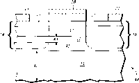
图1是本发明一个实施例的放大剖面图;
图2是图1实施例在零栅偏压下的能带图;
图3是本发明另一实施例的放大剖面图;
图4是本发明又一实施例的放大剖面图;
图5是本发明又一实施例的放大剖面图。
图1示出了根据本发明的具有提高了的载流子迁移率的MOSFET器件10的一个实施例。载流子输运区即沟道层12制作在单晶硅层11上。沟道层12为硅和第二材料的合金。p沟道器件的单晶硅层11为n型导电类型而n沟道器件的单晶硅层11为p型导电类型。第二材料以替位形式出现在沟道层12的晶格位置中,其原子百分比要使沟道层相比于单晶硅层11或含硅晶体来说处于张应力之下。沟道层12最好不要用受主或施主杂质掺杂。
MOSFET器件10还包含形成在沟道层12上的外延半导体即外延层13。外延层13最好含有硅,且厚度为50埃数量级。源区14和漏区16延伸通过外延层13且至少伸入沟道层12。源区14和漏区16最好延伸通过沟道层12进入单晶硅层11之中。一部分沟道层12位于源区14和漏区16之间。控制电极即栅电极18和外延层13电隔离。栅电极18最好用栅介质层17和外延层13电隔离。栅介质层17最好由氧化物构成且其厚度在30—125埃范围内。在部分源区14上制作源电极19并在部分漏区16上制作漏电极21。
图2是图1实施例在零栅偏压下的能带图,示出了应变引入的能带分裂对沟道层12的作用。图2示出了外延层13中、沟道层12中和单晶硅层11中价带22与导带23之间的相对关系。当沟道层12处于张应力下时,沟道层12中的价带边即交界面24分裂,并实际上能级向上移向导带23。此外,导带边即界面26分裂并实际上能级向下移向价带22。这就产生了一个比单晶硅层带隙28和外延层带隙29窄的沟道层带隙27。沟道层带隙27的偏移或变窄实际上产生一个在沟道层12中捕获空穴和电子的势阱。而且,上述效应还使沟道12具有被有效载流子质量降低了的空穴和电子优先占据的能级。当栅电极18加有恰当栅偏压时,这又反过来提高了沟道层12中的自由载流子迁移率。
张应力下的沟道层比压应力下的沟道层更好,这是由于张应力能提供更大的导带分裂。此外,比之压应力下的薄膜,张应力下的薄膜预计有较低的有效载流子质量。于是,张应力下的沟道层可提高电子和空穴载流子的迁移率并保证了迁移率提高了的互补p沟道和n沟道器件的制造。
如授予J.Cande laria和Motorola公司的美国专利5360986(此处作为参考文献)所示,掺碳硅是一种适用于沟道层12的合金材料。在最佳实施例中,沟道层12包含一个掺碳的硅而Si1-xCx合金,其中碳是第二材料,碳位于替位硅晶格位置上,x最好≤0.02。x最好在约0.005—0.016的范围内。
当x为0.02—0.005数量级时,沟道层12的厚度最好分别为100—200埃数量级。根据碳存在的原子百分比来调整沟道层12的厚度。当沟道层12包含Si1-xCx合金时,外延层13最好包含硅且厚度在50—100埃范围内。
由于掺碳沟道层的合金/载流子散射效应较低,故掺碳硅沟道层优于掺Ge硅沟道层。这是由于碳与锗原子间的相对尺寸差使得有可能利用比锗量低很多的碳量(11~1的数量级)来获得相似的应变幅度(尽管符号相反)。由于掺碳硅沟道层的合金/载流子散射效应比有类似应变的掺Ge硅沟道层低,故载流子迁移率,特别是电子迁移率得到了额外的提高。而且,由于MOSFET器件10中的沟道层12是埋置的,亦即以外延层13和单晶硅层11为界,故MOSFET10对表面散射、热载流子退化和噪声效应更不敏感。
当沟道层12含有Si1-xCx合金时,采用外延生长即化学气相淀积技术来制作沟道层12。例如采用乙炔、乙稀、丙烷或甲烷碳源。或者为美国专利5360986所示,制作一个硅层,将碳离子注入到硅层中,并加热掺碳的硅层以诱导掺碳硅层的固相外延再生长以形成沟道层12。或者用分子束外延、金属有机化学气相淀积(MOCVD)或超高真空化学气相淀积(UHVCVD)来制作沟道层12。
在制作带有p沟道结构和掺碳的沟道层的MOSFET10的最佳实施例中,n型导电性单晶硅层11被选择性地形成在p型衬底上或p型衬底中。然后在不掺杂的硅层上形成含有掺碳硅的沟道层12。接着在沟道层12上形成含有n型掺杂硅或不掺杂硅且厚度为50—100埃数量级的外延层13。不掺杂硅层、沟道层12以及外延层13最好在同一个外延生长步骤中形成。
然后在外延层13上沉积或生长一个厚度在60—80埃范围内的氧化硅层。接着在氧化硅层上形成一个原位掺杂的n型多晶硅层。接下来对此n型多晶硅层和氧化硅层进行选择性图形化以分别形成栅电极18和栅介质层17。再将p型杂质选择性地引入外延层13。然后将该结构加热以激活p型杂质而形成源区14和漏区16。再用标准的MOSFET工艺来完成MOSFET器件10。为制作n沟道结构形式的MOSFET器件10,杂质的导电类型正好相反。
图3—5示出了根据本发明的迁移率提高了的MOSFET器件的其它实施例。图3所示MOSFET30除不带有外延层13之外均与MOSFET器件10相似。MOSFET30具有如前所述的提高了的迁移率,但由于沟道层12和栅介质层17之间的界面而对表面散射效应更为敏感。然而,比之结构相似的无应力硅沟道MOSFET器件来说,MOSFET30的载流子迁移率仍然提高了。
图4所示的MOSFET器件40相似于MOSFET器件10,另外还带有形成在单晶硅层11中的调制掺杂层或调制层41。单晶硅层11的43部分将调制层41和沟道层12分隔开来。43部分和厚度最好为50—100埃数量级。调制层41的导电类型与源区14和漏区16相同,其杂质浓度高于单晶硅层11,而且导电类型相反。调制层41的厚度最好在100—200埃的范围内。
调制层41采用外延生长即化学气相淀积(CVD)制作在单晶硅层11的42部位。然后用外延生长或CVD技术在调制层41上制作单晶硅层11的43部分。可用离子注入或扩散技术向单晶硅层11的43部分掺入n型或p型杂质,具体根据MOSFET器件10是p沟道抑或是n沟道器件来决定。调制层41和单晶硅层11的43部分最好在同一个原位工序中相继制作。
图5所示的MOSFET50和MOSFET10相似,另还带有隔离层即区51以形成一个绝缘体上半导体(SOI)器件。隔离层51最好包含氧化硅并用离子注入氧或其它技术来制作。隔离层51最好在形成沟道层12和外延层13之前制作。作为变通,隔离层51可制作在支撑用的衬底(未绘出)上,然后将单晶硅衬底固定到隔离层51上,并将单晶硅衬底减薄至所需的厚度以形成单晶硅层11。隔离层51最好与沟道层12隔开一个500—600埃的距离52。
当隔离层51同MOSFET器件3一起使用时(图3),它最好位于沟道层12下方1000埃数量级处。当隔离层51同MOSFET40一起使用时(图4),它最好位于调制层41下方100—200埃数量级处。
至此应认为已提供了一种迁移率提高了的MOSFET器件。借助于在单晶硅层上制作一个载流子输运区(其中的载流子输运区包含一个硅和第二材料的合金,且第二材料在载流子输运区中的原子百分比使载流子输运区处于张应力之下),获得了提高了的载流子迁移率。
而且,借助于使载流子输运区处于张应力之下,获得了比之载流子输运区处于压应力下更大的导带分裂,从而为电子和空穴载流子都提供了更高的迁移率。这保证了迁移率提高了的互补n沟和p沟器件的制造。
此外,借助于在载流子输运区上增加一个外延层,提供了一个对表面散射、热载流子退化和噪声效应较不敏感的埋置结构。
而且,当载流子输运区包含掺碳硅时,获得了比包含掺锗硅的有类似应变的载流子区更低的合金散射。同时,当载流子输运区包含掺碳硅时,无需采用弛豫合金层就获得了张应力下的载流子输运区。这就降低了工艺的复杂性和成本。
Claims (10)
1.一种迁移率提高了的MOSFET器件,其特征是:
一个第一导电类型的单晶硅层(11);
一个形成在单晶硅层(11)上的载流子输运区(22),其中的载流子输运区(12)由硅与第二半导体材料的合金组成,且其中的第二半导体材料替位地出现在载流子输运区(12)的晶格位置,其原子百分比要使载流子输运区处于张应力之下;
一个延伸到载流子输运区(12)中的第二导电类型的源区(14);
一个延伸到载流子输运区(12)中的第二导电类型的漏区(16),其中载流子输运区(12)的一部分位于源区(14)和漏区(16)之间;以及
一个与载流子输运区(12)电隔离的控制电极(18),其中的控制电极(18)排列在源区(14)和漏区(16)之间。
2.如权利要求1的器件,其进一步特征是:
一个排列在载流子输运区(12)和控制电极(18)之间的第一半导体材料的外延层(13),其中的源区(14)和漏区(16)延伸通过外延层(13)至少进入载流子输运区(12)。
3.如权利要求1的器件,其中的载流于输运区(12)包含Si1-xCx合金。
4.如权利要求3的器件,其中的x≤0.02。
5.一种带有埋置的掺碳的硅沟道区的MOSFET结构,其特征是:
一个沟道层(12),它包含形成在第一导电类型单晶硅层(11)上的Si1-xCx合金,其中的碳出现在沟道层(12)中替位晶格位置上,使沟道(12)处于张应力之下;
一个形成在沟道层上的硅外延层(13);
一个延伸通过硅外延层(13)且至少进入沟道层(12)的第二导电类型的源区(14);
一个延伸通过硅外延层(13)且至少进入沟道层(12)的第二导电类型的漏区(16),其中的部分沟道层(12)将源区(14)与漏区(16)分隔开来;
一个形成在硅外延层(13)上至少位于源区(14)和漏区(16)之间的栅介质层(17);以及
一个形成在栅介质层(17)上的栅电极(18)。
6.如权利要求5的结构,其中的x≤0.02,且其中的单晶硅层(11)的厚度为1000埃的数量级,沟道层(12)的厚度为100埃的数量级,而硅外延层(13)的厚度为50埃数量级。
7.如权利要求5的结构,其进一步特征是:一个排列在单晶硅层(11)下方的隔离区(51)。
8.如权利要求5的结构,其中的单晶硅层(11)包括一个排列在单晶硅层(11)中的调制层(41),其中单晶硅层(11)的一部分将调制层(41)与沟道层(21)分隔开来,且其中的调制层(41)是第二导电类型的,调制层(41)的杂质浓度高于单晶硅层(11)的杂质浓度。
9.一种迁移率提高了的MOSFET器件的制造方法,其特征在于下列步骤:
在第一导电类型的单晶硅层(11)上形成一个载流子输运区(12),其中,载流子输运区(12)包含硅和第二半导体材料的合金,且其中的第二半导体材料替位地出现在载流子输运区(12)的晶格位置,其原子百分比使载流子输运区(12)比之第一导电类型的单晶硅层(11)来说处于张应力之下;
在载流子输运区(12)上形成一个外延半导体层(13);
在一部分载流子输运层(12)上的外延半导体层(13)上形成一个栅介质层(17);
在栅介质层(17)上形成一个控制电极(18);
形成一个延伸通过外延半导体层(13)至少进入载流子输运区(12)的第二导电类型的源区(14);以及
形成一个延伸通过外延半导体层(13)至少进入载流子输运区(12)的第二导电类型的漏区(16),其中部分载流子输运区位于源区(14)和漏区(16)之间。
10.如权利要求9的方法,其中,形成载流子输运区(12)的步骤包括形成一个以Si1-xCx合金为特征的载流子输运区(12),其中的x≤0.02。
Applications Claiming Priority (2)
| Application Number | Priority Date | Filing Date | Title |
|---|---|---|---|
| US08/311,979 US5561302A (en) | 1994-09-26 | 1994-09-26 | Enhanced mobility MOSFET device and method |
| US311979 | 1994-09-26 |
Publications (1)
| Publication Number | Publication Date |
|---|---|
| CN1129358A true CN1129358A (zh) | 1996-08-21 |
Family
ID=23209323
Family Applications (1)
| Application Number | Title | Priority Date | Filing Date |
|---|---|---|---|
| CN95117359A Pending CN1129358A (zh) | 1994-09-26 | 1995-09-25 | 迁移率提高了的mosfet器件及其制造方法 |
Country Status (5)
| Country | Link |
|---|---|
| US (2) | US5561302A (zh) |
| EP (1) | EP0703628A3 (zh) |
| JP (1) | JPH08111528A (zh) |
| KR (1) | KR960012557A (zh) |
| CN (1) | CN1129358A (zh) |
Cited By (7)
| Publication number | Priority date | Publication date | Assignee | Title |
|---|---|---|---|---|
| CN1317772C (zh) * | 2003-06-16 | 2007-05-23 | 松下电器产业株式会社 | 半导体器件及其制造方法 |
| CN1319152C (zh) * | 2000-11-29 | 2007-05-30 | 英特尔公司 | 利用特定晶体管取向的cmos制造方法 |
| CN100421262C (zh) * | 2005-02-25 | 2008-09-24 | 台湾积体电路制造股份有限公司 | 半导体元件 |
| CN101777498A (zh) * | 2010-01-12 | 2010-07-14 | 上海宏力半导体制造有限公司 | 带浅表外延层的外延片形成方法及其外延片 |
| CN101221901B (zh) * | 2007-01-11 | 2012-02-01 | 国际商业机器公司 | 应力绝缘体上硅场效应晶体管及其制作方法 |
| CN104319292A (zh) * | 2014-11-06 | 2015-01-28 | 株洲南车时代电气股份有限公司 | 一种新型碳化硅mosfet及其制造方法 |
| CN104979399A (zh) * | 2014-04-14 | 2015-10-14 | 台湾积体电路制造股份有限公司 | 关于外延沟道器件的错位应力记忆技术 |
Families Citing this family (327)
| Publication number | Priority date | Publication date | Assignee | Title |
|---|---|---|---|---|
| JPH07321323A (ja) * | 1994-05-24 | 1995-12-08 | Matsushita Electric Ind Co Ltd | 薄膜トランジスタおよびその製造方法 |
| JP3243146B2 (ja) * | 1994-12-08 | 2002-01-07 | 株式会社東芝 | 半導体装置 |
| JP3305197B2 (ja) * | 1995-09-14 | 2002-07-22 | 株式会社東芝 | 半導体装置 |
| JP2839018B2 (ja) * | 1996-07-31 | 1998-12-16 | 日本電気株式会社 | 半導体装置の製造方法 |
| US6399970B2 (en) | 1996-09-17 | 2002-06-04 | Matsushita Electric Industrial Co., Ltd. | FET having a Si/SiGeC heterojunction channel |
| JP3461274B2 (ja) * | 1996-10-16 | 2003-10-27 | 株式会社東芝 | 半導体装置 |
| JPH10270685A (ja) | 1997-03-27 | 1998-10-09 | Sony Corp | 電界効果トランジスタとその製造方法、半導体装置とその製造方法、その半導体装置を含む論理回路および半導体基板 |
| US5891769A (en) * | 1997-04-07 | 1999-04-06 | Motorola, Inc. | Method for forming a semiconductor device having a heteroepitaxial layer |
| CA2295069A1 (en) | 1997-06-24 | 1998-12-30 | Eugene A. Fitzgerald | Controlling threading dislocation densities in ge on si using graded gesi layers and planarization |
| JP3443343B2 (ja) * | 1997-12-03 | 2003-09-02 | 松下電器産業株式会社 | 半導体装置 |
| US7227176B2 (en) | 1998-04-10 | 2007-06-05 | Massachusetts Institute Of Technology | Etch stop layer system |
| JP3592981B2 (ja) * | 1999-01-14 | 2004-11-24 | 松下電器産業株式会社 | 半導体装置及びその製造方法 |
| US6350993B1 (en) | 1999-03-12 | 2002-02-26 | International Business Machines Corporation | High speed composite p-channel Si/SiGe heterostructure for field effect devices |
| US6281532B1 (en) * | 1999-06-28 | 2001-08-28 | Intel Corporation | Technique to obtain increased channel mobilities in NMOS transistors by gate electrode engineering |
| US6656822B2 (en) | 1999-06-28 | 2003-12-02 | Intel Corporation | Method for reduced capacitance interconnect system using gaseous implants into the ILD |
| EP1102327B1 (en) * | 1999-11-15 | 2007-10-03 | Matsushita Electric Industrial Co., Ltd. | Field effect semiconductor device |
| JP2003520444A (ja) | 2000-01-20 | 2003-07-02 | アンバーウェーブ システムズ コーポレイション | 高温成長を不要とする低貫通転位密度格子不整合エピ層 |
| US6750130B1 (en) | 2000-01-20 | 2004-06-15 | Amberwave Systems Corporation | Heterointegration of materials using deposition and bonding |
| US6602613B1 (en) | 2000-01-20 | 2003-08-05 | Amberwave Systems Corporation | Heterointegration of materials using deposition and bonding |
| DE10025264A1 (de) * | 2000-05-22 | 2001-11-29 | Max Planck Gesellschaft | Feldeffekt-Transistor auf der Basis von eingebetteten Clusterstrukturen und Verfahren zu seiner Herstellung |
| AU2001263211A1 (en) * | 2000-05-26 | 2001-12-11 | Amberwave Systems Corporation | Buried channel strained silicon fet using an ion implanted doped layer |
| US6461945B1 (en) | 2000-06-22 | 2002-10-08 | Advanced Micro Devices, Inc. | Solid phase epitaxy process for manufacturing transistors having silicon/germanium channel regions |
| US6743680B1 (en) * | 2000-06-22 | 2004-06-01 | Advanced Micro Devices, Inc. | Process for manufacturing transistors having silicon/germanium channel regions |
| US6521502B1 (en) | 2000-08-07 | 2003-02-18 | Advanced Micro Devices, Inc. | Solid phase epitaxy activation process for source/drain junction extensions and halo regions |
| JP2004519090A (ja) * | 2000-08-07 | 2004-06-24 | アンバーウェーブ システムズ コーポレイション | 歪み表面チャネル及び歪み埋め込みチャネルmosfet素子のゲート技術 |
| US6573126B2 (en) | 2000-08-16 | 2003-06-03 | Massachusetts Institute Of Technology | Process for producing semiconductor article using graded epitaxial growth |
| US6544854B1 (en) * | 2000-11-28 | 2003-04-08 | Lsi Logic Corporation | Silicon germanium CMOS channel |
| US6831263B2 (en) | 2002-06-04 | 2004-12-14 | Intel Corporation | Very high speed photodetector system using a PIN photodiode array for position sensing |
| US20020100942A1 (en) * | 2000-12-04 | 2002-08-01 | Fitzgerald Eugene A. | CMOS inverter and integrated circuits utilizing strained silicon surface channel MOSFETs |
| US6649480B2 (en) | 2000-12-04 | 2003-11-18 | Amberwave Systems Corporation | Method of fabricating CMOS inverter and integrated circuits utilizing strained silicon surface channel MOSFETs |
| US6844227B2 (en) * | 2000-12-26 | 2005-01-18 | Matsushita Electric Industrial Co., Ltd. | Semiconductor devices and method for manufacturing the same |
| US6495402B1 (en) | 2001-02-06 | 2002-12-17 | Advanced Micro Devices, Inc. | Semiconductor-on-insulator (SOI) device having source/drain silicon-germanium regions and method of manufacture |
| US6380590B1 (en) | 2001-02-22 | 2002-04-30 | Advanced Micro Devices, Inc. | SOI chip having multiple threshold voltage MOSFETs by using multiple channel materials and method of fabricating same |
| US6475869B1 (en) | 2001-02-26 | 2002-11-05 | Advanced Micro Devices, Inc. | Method of forming a double gate transistor having an epitaxial silicon/germanium channel region |
| US6410371B1 (en) | 2001-02-26 | 2002-06-25 | Advanced Micro Devices, Inc. | Method of fabrication of semiconductor-on-insulator (SOI) wafer having a Si/SiGe/Si active layer |
| US6677192B1 (en) | 2001-03-02 | 2004-01-13 | Amberwave Systems Corporation | Method of fabricating a relaxed silicon germanium platform having planarizing for high speed CMOS electronics and high speed analog circuits |
| US6703688B1 (en) | 2001-03-02 | 2004-03-09 | Amberwave Systems Corporation | Relaxed silicon germanium platform for high speed CMOS electronics and high speed analog circuits |
| US6900103B2 (en) | 2001-03-02 | 2005-05-31 | Amberwave Systems Corporation | Relaxed silicon germanium platform for high speed CMOS electronics and high speed analog circuits |
| US6724008B2 (en) | 2001-03-02 | 2004-04-20 | Amberwave Systems Corporation | Relaxed silicon germanium platform for high speed CMOS electronics and high speed analog circuits |
| US6593641B1 (en) | 2001-03-02 | 2003-07-15 | Amberwave Systems Corporation | Relaxed silicon germanium platform for high speed CMOS electronics and high speed analog circuits |
| US6830976B2 (en) * | 2001-03-02 | 2004-12-14 | Amberwave Systems Corproation | Relaxed silicon germanium platform for high speed CMOS electronics and high speed analog circuits |
| US6723661B2 (en) | 2001-03-02 | 2004-04-20 | Amberwave Systems Corporation | Relaxed silicon germanium platform for high speed CMOS electronics and high speed analog circuits |
| US6646322B2 (en) | 2001-03-02 | 2003-11-11 | Amberwave Systems Corporation | Relaxed silicon germanium platform for high speed CMOS electronics and high speed analog circuits |
| US6709935B1 (en) | 2001-03-26 | 2004-03-23 | Advanced Micro Devices, Inc. | Method of locally forming a silicon/geranium channel layer |
| US6921743B2 (en) * | 2001-04-02 | 2005-07-26 | The Procter & Gamble Company | Automatic dishwashing compositions containing a halogen dioxide salt and methods for use with electrochemical cells and/or electrolytic devices |
| WO2002082514A1 (en) | 2001-04-04 | 2002-10-17 | Massachusetts Institute Of Technology | A method for semiconductor device fabrication |
| US6750119B2 (en) | 2001-04-20 | 2004-06-15 | International Business Machines Corporation | Epitaxial and polycrystalline growth of Si1-x-yGexCy and Si1-yCy alloy layers on Si by UHV-CVD |
| US6900094B2 (en) * | 2001-06-14 | 2005-05-31 | Amberwave Systems Corporation | Method of selective removal of SiGe alloys |
| US7301180B2 (en) | 2001-06-18 | 2007-11-27 | Massachusetts Institute Of Technology | Structure and method for a high-speed semiconductor device having a Ge channel layer |
| US6916727B2 (en) * | 2001-06-21 | 2005-07-12 | Massachusetts Institute Of Technology | Enhancement of P-type metal-oxide-semiconductor field effect transistors |
| WO2003015142A2 (en) | 2001-08-06 | 2003-02-20 | Massachusetts Institute Of Technology | Formation of planar strained layers |
| US7138649B2 (en) | 2001-08-09 | 2006-11-21 | Amberwave Systems Corporation | Dual-channel CMOS transistors with differentially strained channels |
| US6974735B2 (en) * | 2001-08-09 | 2005-12-13 | Amberwave Systems Corporation | Dual layer Semiconductor Devices |
| KR100425462B1 (ko) * | 2001-09-10 | 2004-03-30 | 삼성전자주식회사 | Soi 상의 반도체 장치 및 그의 제조방법 |
| US6831292B2 (en) | 2001-09-21 | 2004-12-14 | Amberwave Systems Corporation | Semiconductor structures employing strained material layers with defined impurity gradients and methods for fabricating same |
| WO2003028106A2 (en) * | 2001-09-24 | 2003-04-03 | Amberwave Systems Corporation | Rf circuits including transistors having strained material layers |
| KR20030035152A (ko) * | 2001-10-30 | 2003-05-09 | 주식회사 하이닉스반도체 | 반도체웨이퍼 제조방법 |
| US6621131B2 (en) * | 2001-11-01 | 2003-09-16 | Intel Corporation | Semiconductor transistor having a stressed channel |
| JP2003179157A (ja) | 2001-12-10 | 2003-06-27 | Nec Corp | Mos型半導体装置 |
| US6657276B1 (en) | 2001-12-10 | 2003-12-02 | Advanced Micro Devices, Inc. | Shallow trench isolation (STI) region with high-K liner and method of formation |
| US6806151B2 (en) * | 2001-12-14 | 2004-10-19 | Texas Instruments Incorporated | Methods and apparatus for inducing stress in a semiconductor device |
| US7060632B2 (en) | 2002-03-14 | 2006-06-13 | Amberwave Systems Corporation | Methods for fabricating strained layers on semiconductor substrates |
| AU2003238963A1 (en) * | 2002-06-07 | 2003-12-22 | Amberwave Systems Corporation | Semiconductor devices having strained dual channel layers |
| US20030227057A1 (en) | 2002-06-07 | 2003-12-11 | Lochtefeld Anthony J. | Strained-semiconductor-on-insulator device structures |
| US7615829B2 (en) | 2002-06-07 | 2009-11-10 | Amberwave Systems Corporation | Elevated source and drain elements for strained-channel heterojuntion field-effect transistors |
| US7307273B2 (en) | 2002-06-07 | 2007-12-11 | Amberwave Systems Corporation | Control of strain in device layers by selective relaxation |
| US7074623B2 (en) | 2002-06-07 | 2006-07-11 | Amberwave Systems Corporation | Methods of forming strained-semiconductor-on-insulator finFET device structures |
| US6995430B2 (en) | 2002-06-07 | 2006-02-07 | Amberwave Systems Corporation | Strained-semiconductor-on-insulator device structures |
| US7335545B2 (en) | 2002-06-07 | 2008-02-26 | Amberwave Systems Corporation | Control of strain in device layers by prevention of relaxation |
| AU2003247513A1 (en) | 2002-06-10 | 2003-12-22 | Amberwave Systems Corporation | Growing source and drain elements by selecive epitaxy |
| US6982474B2 (en) | 2002-06-25 | 2006-01-03 | Amberwave Systems Corporation | Reacted conductive gate electrodes |
| US6680240B1 (en) | 2002-06-25 | 2004-01-20 | Advanced Micro Devices, Inc. | Silicon-on-insulator device with strained device film and method for making the same with partial replacement of isolation oxide |
| US6605514B1 (en) | 2002-07-31 | 2003-08-12 | Advanced Micro Devices, Inc. | Planar finFET patterning using amorphous carbon |
| AU2003274922A1 (en) | 2002-08-23 | 2004-03-11 | Amberwave Systems Corporation | Semiconductor heterostructures having reduced dislocation pile-ups and related methods |
| US7594967B2 (en) | 2002-08-30 | 2009-09-29 | Amberwave Systems Corporation | Reduction of dislocation pile-up formation during relaxed lattice-mismatched epitaxy |
| US6573172B1 (en) | 2002-09-16 | 2003-06-03 | Advanced Micro Devices, Inc. | Methods for improving carrier mobility of PMOS and NMOS devices |
| CN1286157C (zh) * | 2002-10-10 | 2006-11-22 | 松下电器产业株式会社 | 半导体装置及其制造方法 |
| US7388259B2 (en) * | 2002-11-25 | 2008-06-17 | International Business Machines Corporation | Strained finFET CMOS device structures |
| US6825506B2 (en) * | 2002-11-27 | 2004-11-30 | Intel Corporation | Field effect transistor and method of fabrication |
| US7001837B2 (en) * | 2003-01-17 | 2006-02-21 | Advanced Micro Devices, Inc. | Semiconductor with tensile strained substrate and method of making the same |
| EP2337062A3 (en) | 2003-01-27 | 2016-05-04 | Taiwan Semiconductor Manufacturing Company, Limited | Method for making semiconductor structures with structural homogeneity |
| US6921913B2 (en) * | 2003-03-04 | 2005-07-26 | Taiwan Semiconductor Manufacturing Co., Ltd. | Strained-channel transistor structure with lattice-mismatched zone |
| EP1602125B1 (en) | 2003-03-07 | 2019-06-26 | Taiwan Semiconductor Manufacturing Company, Ltd. | Shallow trench isolation process |
| US6887798B2 (en) * | 2003-05-30 | 2005-05-03 | International Business Machines Corporation | STI stress modification by nitrogen plasma treatment for improving performance in small width devices |
| KR100500451B1 (ko) * | 2003-06-16 | 2005-07-12 | 삼성전자주식회사 | 인장된 채널을 갖는 모스 트랜지스터를 구비하는반도체소자의 제조 방법 |
| US7329923B2 (en) * | 2003-06-17 | 2008-02-12 | International Business Machines Corporation | High-performance CMOS devices on hybrid crystal oriented substrates |
| US7531828B2 (en) * | 2003-06-26 | 2009-05-12 | Mears Technologies, Inc. | Semiconductor device including a strained superlattice between at least one pair of spaced apart stress regions |
| US20060231857A1 (en) * | 2003-06-26 | 2006-10-19 | Rj Mears, Llc | Method for making a semiconductor device including a memory cell with a negative differential resistance (ndr) device |
| US7045813B2 (en) * | 2003-06-26 | 2006-05-16 | Rj Mears, Llc | Semiconductor device including a superlattice with regions defining a semiconductor junction |
| US20060267130A1 (en) * | 2003-06-26 | 2006-11-30 | Rj Mears, Llc | Semiconductor Device Including Shallow Trench Isolation (STI) Regions with a Superlattice Therebetween |
| WO2005018005A1 (en) * | 2003-06-26 | 2005-02-24 | Rj Mears, Llc | Semiconductor device including mosfet having band-engineered superlattice |
| US7659539B2 (en) | 2003-06-26 | 2010-02-09 | Mears Technologies, Inc. | Semiconductor device including a floating gate memory cell with a superlattice channel |
| US7586165B2 (en) * | 2003-06-26 | 2009-09-08 | Mears Technologies, Inc. | Microelectromechanical systems (MEMS) device including a superlattice |
| US20060243964A1 (en) * | 2003-06-26 | 2006-11-02 | Rj Mears, Llc | Method for making a semiconductor device having a semiconductor-on-insulator configuration and a superlattice |
| US20060289049A1 (en) * | 2003-06-26 | 2006-12-28 | Rj Mears, Llc | Semiconductor Device Having a Semiconductor-on-Insulator (SOI) Configuration and Including a Superlattice on a Thin Semiconductor Layer |
| US7491587B2 (en) * | 2003-06-26 | 2009-02-17 | Mears Technologies, Inc. | Method for making a semiconductor device having a semiconductor-on-insulator (SOI) configuration and including a superlattice on a thin semiconductor layer |
| US20070063186A1 (en) * | 2003-06-26 | 2007-03-22 | Rj Mears, Llc | Method for making a semiconductor device including a front side strained superlattice layer and a back side stress layer |
| US20060273299A1 (en) * | 2003-06-26 | 2006-12-07 | Rj Mears, Llc | Method for making a semiconductor device including a dopant blocking superlattice |
| US20060220118A1 (en) * | 2003-06-26 | 2006-10-05 | Rj Mears, Llc | Semiconductor device including a dopant blocking superlattice |
| US20040262594A1 (en) * | 2003-06-26 | 2004-12-30 | Rj Mears, Llc | Semiconductor structures having improved conductivity effective mass and methods for fabricating same |
| US7202494B2 (en) * | 2003-06-26 | 2007-04-10 | Rj Mears, Llc | FINFET including a superlattice |
| US7229902B2 (en) * | 2003-06-26 | 2007-06-12 | Rj Mears, Llc | Method for making a semiconductor device including a superlattice with regions defining a semiconductor junction |
| US7531850B2 (en) * | 2003-06-26 | 2009-05-12 | Mears Technologies, Inc. | Semiconductor device including a memory cell with a negative differential resistance (NDR) device |
| US20050282330A1 (en) * | 2003-06-26 | 2005-12-22 | Rj Mears, Llc | Method for making a semiconductor device including a superlattice having at least one group of substantially undoped layers |
| US7598515B2 (en) * | 2003-06-26 | 2009-10-06 | Mears Technologies, Inc. | Semiconductor device including a strained superlattice and overlying stress layer and related methods |
| US6958486B2 (en) * | 2003-06-26 | 2005-10-25 | Rj Mears, Llc | Semiconductor device including band-engineered superlattice |
| US7531829B2 (en) * | 2003-06-26 | 2009-05-12 | Mears Technologies, Inc. | Semiconductor device including regions of band-engineered semiconductor superlattice to reduce device-on resistance |
| US20070015344A1 (en) * | 2003-06-26 | 2007-01-18 | Rj Mears, Llc | Method for Making a Semiconductor Device Including a Strained Superlattice Between at Least One Pair of Spaced Apart Stress Regions |
| US7514328B2 (en) * | 2003-06-26 | 2009-04-07 | Mears Technologies, Inc. | Method for making a semiconductor device including shallow trench isolation (STI) regions with a superlattice therebetween |
| US7153763B2 (en) | 2003-06-26 | 2006-12-26 | Rj Mears, Llc | Method for making a semiconductor device including band-engineered superlattice using intermediate annealing |
| US7045377B2 (en) * | 2003-06-26 | 2006-05-16 | Rj Mears, Llc | Method for making a semiconductor device including a superlattice and adjacent semiconductor layer with doped regions defining a semiconductor junction |
| US20070020860A1 (en) * | 2003-06-26 | 2007-01-25 | Rj Mears, Llc | Method for Making Semiconductor Device Including a Strained Superlattice and Overlying Stress Layer and Related Methods |
| US7446002B2 (en) * | 2003-06-26 | 2008-11-04 | Mears Technologies, Inc. | Method for making a semiconductor device comprising a superlattice dielectric interface layer |
| US7612366B2 (en) * | 2003-06-26 | 2009-11-03 | Mears Technologies, Inc. | Semiconductor device including a strained superlattice layer above a stress layer |
| US20060011905A1 (en) * | 2003-06-26 | 2006-01-19 | Rj Mears, Llc | Semiconductor device comprising a superlattice dielectric interface layer |
| US20070020833A1 (en) * | 2003-06-26 | 2007-01-25 | Rj Mears, Llc | Method for Making a Semiconductor Device Including a Channel with a Non-Semiconductor Layer Monolayer |
| US20040266116A1 (en) * | 2003-06-26 | 2004-12-30 | Rj Mears, Llc | Methods of fabricating semiconductor structures having improved conductivity effective mass |
| US7227174B2 (en) * | 2003-06-26 | 2007-06-05 | Rj Mears, Llc | Semiconductor device including a superlattice and adjacent semiconductor layer with doped regions defining a semiconductor junction |
| US6833294B1 (en) | 2003-06-26 | 2004-12-21 | Rj Mears, Llc | Method for making semiconductor device including band-engineered superlattice |
| US20050279991A1 (en) * | 2003-06-26 | 2005-12-22 | Rj Mears, Llc | Semiconductor device including a superlattice having at least one group of substantially undoped layers |
| US20070063185A1 (en) * | 2003-06-26 | 2007-03-22 | Rj Mears, Llc | Semiconductor device including a front side strained superlattice layer and a back side stress layer |
| US7535041B2 (en) * | 2003-06-26 | 2009-05-19 | Mears Technologies, Inc. | Method for making a semiconductor device including regions of band-engineered semiconductor superlattice to reduce device-on resistance |
| US20070010040A1 (en) * | 2003-06-26 | 2007-01-11 | Rj Mears, Llc | Method for Making a Semiconductor Device Including a Strained Superlattice Layer Above a Stress Layer |
| US7586116B2 (en) * | 2003-06-26 | 2009-09-08 | Mears Technologies, Inc. | Semiconductor device having a semiconductor-on-insulator configuration and a superlattice |
| US20060292765A1 (en) * | 2003-06-26 | 2006-12-28 | Rj Mears, Llc | Method for Making a FINFET Including a Superlattice |
| US7279746B2 (en) * | 2003-06-30 | 2007-10-09 | International Business Machines Corporation | High performance CMOS device structures and method of manufacture |
| US7410846B2 (en) * | 2003-09-09 | 2008-08-12 | International Business Machines Corporation | Method for reduced N+ diffusion in strained Si on SiGe substrate |
| US6890808B2 (en) * | 2003-09-10 | 2005-05-10 | International Business Machines Corporation | Method and structure for improved MOSFETs using poly/silicide gate height control |
| US6887751B2 (en) * | 2003-09-12 | 2005-05-03 | International Business Machines Corporation | MOSFET performance improvement using deformation in SOI structure |
| US7170126B2 (en) * | 2003-09-16 | 2007-01-30 | International Business Machines Corporation | Structure of vertical strained silicon devices |
| US6869866B1 (en) | 2003-09-22 | 2005-03-22 | International Business Machines Corporation | Silicide proximity structures for CMOS device performance improvements |
| US7144767B2 (en) * | 2003-09-23 | 2006-12-05 | International Business Machines Corporation | NFETs using gate induced stress modulation |
| US6872641B1 (en) * | 2003-09-23 | 2005-03-29 | International Business Machines Corporation | Strained silicon on relaxed sige film with uniform misfit dislocation density |
| US7119403B2 (en) | 2003-10-16 | 2006-10-10 | International Business Machines Corporation | High performance strained CMOS devices |
| US7037770B2 (en) * | 2003-10-20 | 2006-05-02 | International Business Machines Corporation | Method of manufacturing strained dislocation-free channels for CMOS |
| US7303949B2 (en) * | 2003-10-20 | 2007-12-04 | International Business Machines Corporation | High performance stress-enhanced MOSFETs using Si:C and SiGe epitaxial source/drain and method of manufacture |
| US7129126B2 (en) * | 2003-11-05 | 2006-10-31 | International Business Machines Corporation | Method and structure for forming strained Si for CMOS devices |
| US7015082B2 (en) * | 2003-11-06 | 2006-03-21 | International Business Machines Corporation | High mobility CMOS circuits |
| US7029964B2 (en) * | 2003-11-13 | 2006-04-18 | International Business Machines Corporation | Method of manufacturing a strained silicon on a SiGe on SOI substrate |
| US20050108101A1 (en) * | 2003-11-13 | 2005-05-19 | Taiwan Semiconductor Manufacturing Co., Ltd. | Method and system to link orders with quotations |
| US7122849B2 (en) * | 2003-11-14 | 2006-10-17 | International Business Machines Corporation | Stressed semiconductor device structures having granular semiconductor material |
| US7247534B2 (en) | 2003-11-19 | 2007-07-24 | International Business Machines Corporation | Silicon device on Si:C-OI and SGOI and method of manufacture |
| US7198995B2 (en) * | 2003-12-12 | 2007-04-03 | International Business Machines Corporation | Strained finFETs and method of manufacture |
| US7005333B2 (en) * | 2003-12-30 | 2006-02-28 | Infineon Technologies Ag | Transistor with silicon and carbon layer in the channel region |
| US7247912B2 (en) * | 2004-01-05 | 2007-07-24 | International Business Machines Corporation | Structures and methods for making strained MOSFETs |
| US7381609B2 (en) | 2004-01-16 | 2008-06-03 | International Business Machines Corporation | Method and structure for controlling stress in a transistor channel |
| US7118999B2 (en) * | 2004-01-16 | 2006-10-10 | International Business Machines Corporation | Method and apparatus to increase strain effect in a transistor channel |
| US7202132B2 (en) | 2004-01-16 | 2007-04-10 | International Business Machines Corporation | Protecting silicon germanium sidewall with silicon for strained silicon/silicon germanium MOSFETs |
| US7407837B2 (en) | 2004-01-27 | 2008-08-05 | Fuji Electric Holdings Co., Ltd. | Method of manufacturing silicon carbide semiconductor device |
| US7002224B2 (en) * | 2004-02-03 | 2006-02-21 | Infineon Technologies Ag | Transistor with doped gate dielectric |
| US7923782B2 (en) | 2004-02-27 | 2011-04-12 | International Business Machines Corporation | Hybrid SOI/bulk semiconductor transistors |
| SE527487C2 (sv) * | 2004-03-02 | 2006-03-21 | Infineon Technologies Ag | En metod för framställning av en kondensator och en monolitiskt integrerad krets innefattande en sådan kondensator |
| US7205206B2 (en) * | 2004-03-03 | 2007-04-17 | International Business Machines Corporation | Method of fabricating mobility enhanced CMOS devices |
| US7094671B2 (en) * | 2004-03-22 | 2006-08-22 | Infineon Technologies Ag | Transistor with shallow germanium implantation region in channel |
| US7226834B2 (en) * | 2004-04-19 | 2007-06-05 | Texas Instruments Incorporated | PMD liner nitride films and fabrication methods for improved NMOS performance |
| US7504693B2 (en) | 2004-04-23 | 2009-03-17 | International Business Machines Corporation | Dislocation free stressed channels in bulk silicon and SOI CMOS devices by gate stress engineering |
| US7223994B2 (en) * | 2004-06-03 | 2007-05-29 | International Business Machines Corporation | Strained Si on multiple materials for bulk or SOI substrates |
| US7037794B2 (en) * | 2004-06-09 | 2006-05-02 | International Business Machines Corporation | Raised STI process for multiple gate ox and sidewall protection on strained Si/SGOI structure with elevated source/drain |
| US7227205B2 (en) * | 2004-06-24 | 2007-06-05 | International Business Machines Corporation | Strained-silicon CMOS device and method |
| TWI463526B (zh) * | 2004-06-24 | 2014-12-01 | Ibm | 改良具應力矽之cmos元件的方法及以該方法製備而成的元件 |
| US7288443B2 (en) * | 2004-06-29 | 2007-10-30 | International Business Machines Corporation | Structures and methods for manufacturing p-type MOSFET with graded embedded silicon-germanium source-drain and/or extension |
| US7217949B2 (en) * | 2004-07-01 | 2007-05-15 | International Business Machines Corporation | Strained Si MOSFET on tensile-strained SiGe-on-insulator (SGOI) |
| US6991998B2 (en) * | 2004-07-02 | 2006-01-31 | International Business Machines Corporation | Ultra-thin, high quality strained silicon-on-insulator formed by elastic strain transfer |
| US7384829B2 (en) | 2004-07-23 | 2008-06-10 | International Business Machines Corporation | Patterned strained semiconductor substrate and device |
| US7217626B2 (en) * | 2004-07-26 | 2007-05-15 | Texas Instruments Incorporated | Transistor fabrication methods using dual sidewall spacers |
| US7012028B2 (en) * | 2004-07-26 | 2006-03-14 | Texas Instruments Incorporated | Transistor fabrication methods using reduced width sidewall spacers |
| US7279430B2 (en) * | 2004-08-17 | 2007-10-09 | Taiwan Semiconductor Manufacturing Company, Ltd. | Process for fabricating a strained channel MOSFET device |
| US7235812B2 (en) * | 2004-09-13 | 2007-06-26 | International Business Machines Corporation | Method of creating defect free high Ge content (>25%) SiGe-on-insulator (SGOI) substrates using wafer bonding techniques |
| US7129127B2 (en) * | 2004-09-24 | 2006-10-31 | Texas Instruments Incorporated | Integration scheme to improve NMOS with poly cap while mitigating PMOS degradation |
| US7172936B2 (en) * | 2004-09-24 | 2007-02-06 | Texas Instruments Incorporated | Method to selectively strain NMOS devices using a cap poly layer |
| US7193254B2 (en) * | 2004-11-30 | 2007-03-20 | International Business Machines Corporation | Structure and method of applying stresses to PFET and NFET transistor channels for improved performance |
| US20060113603A1 (en) * | 2004-12-01 | 2006-06-01 | Amberwave Systems Corporation | Hybrid semiconductor-on-insulator structures and related methods |
| US7393733B2 (en) | 2004-12-01 | 2008-07-01 | Amberwave Systems Corporation | Methods of forming hybrid fin field-effect transistor structures |
| US7238565B2 (en) * | 2004-12-08 | 2007-07-03 | International Business Machines Corporation | Methodology for recovery of hot carrier induced degradation in bipolar devices |
| US7262087B2 (en) * | 2004-12-14 | 2007-08-28 | International Business Machines Corporation | Dual stressed SOI substrates |
| US7173312B2 (en) * | 2004-12-15 | 2007-02-06 | International Business Machines Corporation | Structure and method to generate local mechanical gate stress for MOSFET channel mobility modification |
| US7274084B2 (en) * | 2005-01-12 | 2007-09-25 | International Business Machines Corporation | Enhanced PFET using shear stress |
| US20060160317A1 (en) * | 2005-01-18 | 2006-07-20 | International Business Machines Corporation | Structure and method to enhance stress in a channel of cmos devices using a thin gate |
| US7432553B2 (en) * | 2005-01-19 | 2008-10-07 | International Business Machines Corporation | Structure and method to optimize strain in CMOSFETs |
| US7220626B2 (en) * | 2005-01-28 | 2007-05-22 | International Business Machines Corporation | Structure and method for manufacturing planar strained Si/SiGe substrate with multiple orientations and different stress levels |
| US7256081B2 (en) * | 2005-02-01 | 2007-08-14 | International Business Machines Corporation | Structure and method to induce strain in a semiconductor device channel with stressed film under the gate |
| US7224033B2 (en) * | 2005-02-15 | 2007-05-29 | International Business Machines Corporation | Structure and method for manufacturing strained FINFET |
| US7545004B2 (en) * | 2005-04-12 | 2009-06-09 | International Business Machines Corporation | Method and structure for forming strained devices |
| JP4948784B2 (ja) * | 2005-05-19 | 2012-06-06 | 三菱電機株式会社 | 半導体装置及びその製造方法 |
| US7528028B2 (en) * | 2005-06-17 | 2009-05-05 | Taiwan Semiconductor Manufacturing Company, Ltd. | Super anneal for process induced strain modulation |
| US20070010073A1 (en) * | 2005-07-06 | 2007-01-11 | Chien-Hao Chen | Method of forming a MOS device having a strained channel region |
| US7544577B2 (en) * | 2005-08-26 | 2009-06-09 | International Business Machines Corporation | Mobility enhancement in SiGe heterojunction bipolar transistors |
| US7202513B1 (en) * | 2005-09-29 | 2007-04-10 | International Business Machines Corporation | Stress engineering using dual pad nitride with selective SOI device architecture |
| US20070096170A1 (en) * | 2005-11-02 | 2007-05-03 | International Business Machines Corporation | Low modulus spacers for channel stress enhancement |
| US7655511B2 (en) | 2005-11-03 | 2010-02-02 | International Business Machines Corporation | Gate electrode stress control for finFET performance enhancement |
| US20070099360A1 (en) * | 2005-11-03 | 2007-05-03 | International Business Machines Corporation | Integrated circuits having strained channel field effect transistors and methods of making |
| US7785950B2 (en) * | 2005-11-10 | 2010-08-31 | International Business Machines Corporation | Dual stress memory technique method and related structure |
| US7709317B2 (en) * | 2005-11-14 | 2010-05-04 | International Business Machines Corporation | Method to increase strain enhancement with spacerless FET and dual liner process |
| US7348638B2 (en) * | 2005-11-14 | 2008-03-25 | International Business Machines Corporation | Rotational shear stress for charge carrier mobility modification |
| US7564081B2 (en) * | 2005-11-30 | 2009-07-21 | International Business Machines Corporation | finFET structure with multiply stressed gate electrode |
| TWI316294B (en) * | 2005-12-22 | 2009-10-21 | Mears Technologies Inc | Method for making an electronic device including a selectively polable superlattice |
| US7517702B2 (en) * | 2005-12-22 | 2009-04-14 | Mears Technologies, Inc. | Method for making an electronic device including a poled superlattice having a net electrical dipole moment |
| US7776695B2 (en) * | 2006-01-09 | 2010-08-17 | International Business Machines Corporation | Semiconductor device structure having low and high performance devices of same conductive type on same substrate |
| US7863197B2 (en) * | 2006-01-09 | 2011-01-04 | International Business Machines Corporation | Method of forming a cross-section hourglass shaped channel region for charge carrier mobility modification |
| US7635620B2 (en) * | 2006-01-10 | 2009-12-22 | International Business Machines Corporation | Semiconductor device structure having enhanced performance FET device |
| US20070158743A1 (en) * | 2006-01-11 | 2007-07-12 | International Business Machines Corporation | Thin silicon single diffusion field effect transistor for enhanced drive performance with stress film liners |
| US8900980B2 (en) * | 2006-01-20 | 2014-12-02 | Taiwan Semiconductor Manufacturing Company, Ltd. | Defect-free SiGe source/drain formation by epitaxy-free process |
| US7718996B2 (en) * | 2006-02-21 | 2010-05-18 | Mears Technologies, Inc. | Semiconductor device comprising a lattice matching layer |
| US7691698B2 (en) | 2006-02-21 | 2010-04-06 | International Business Machines Corporation | Pseudomorphic Si/SiGe/Si body device with embedded SiGe source/drain |
| US8461009B2 (en) * | 2006-02-28 | 2013-06-11 | International Business Machines Corporation | Spacer and process to enhance the strain in the channel with stress liner |
| US7521307B2 (en) | 2006-04-28 | 2009-04-21 | International Business Machines Corporation | CMOS structures and methods using self-aligned dual stressed layers |
| US7615418B2 (en) * | 2006-04-28 | 2009-11-10 | International Business Machines Corporation | High performance stress-enhance MOSFET and method of manufacture |
| US7608489B2 (en) * | 2006-04-28 | 2009-10-27 | International Business Machines Corporation | High performance stress-enhance MOSFET and method of manufacture |
| US8853746B2 (en) * | 2006-06-29 | 2014-10-07 | International Business Machines Corporation | CMOS devices with stressed channel regions, and methods for fabricating the same |
| US7790540B2 (en) | 2006-08-25 | 2010-09-07 | International Business Machines Corporation | Structure and method to use low k stress liner to reduce parasitic capacitance |
| US7462522B2 (en) * | 2006-08-30 | 2008-12-09 | International Business Machines Corporation | Method and structure for improving device performance variation in dual stress liner technology |
| US8754446B2 (en) * | 2006-08-30 | 2014-06-17 | International Business Machines Corporation | Semiconductor structure having undercut-gate-oxide gate stack enclosed by protective barrier material |
| US7741200B2 (en) * | 2006-12-01 | 2010-06-22 | Applied Materials, Inc. | Formation and treatment of epitaxial layer containing silicon and carbon |
| US7781827B2 (en) | 2007-01-24 | 2010-08-24 | Mears Technologies, Inc. | Semiconductor device with a vertical MOSFET including a superlattice and related methods |
| US7928425B2 (en) * | 2007-01-25 | 2011-04-19 | Mears Technologies, Inc. | Semiconductor device including a metal-to-semiconductor superlattice interface layer and related methods |
| US7880161B2 (en) | 2007-02-16 | 2011-02-01 | Mears Technologies, Inc. | Multiple-wavelength opto-electronic device including a superlattice |
| US7863066B2 (en) * | 2007-02-16 | 2011-01-04 | Mears Technologies, Inc. | Method for making a multiple-wavelength opto-electronic device including a superlattice |
| US7812339B2 (en) * | 2007-04-23 | 2010-10-12 | Mears Technologies, Inc. | Method for making a semiconductor device including shallow trench isolation (STI) regions with maskless superlattice deposition following STI formation and related structures |
| TW200910470A (en) * | 2007-05-03 | 2009-03-01 | Dsm Solutions Inc | Enhanced hole mobility p-type JFET and fabrication method therefor |
| US7795119B2 (en) * | 2007-07-17 | 2010-09-14 | Taiwan Semiconductor Manufacturing Company, Ltd. | Flash anneal for a PAI, NiSi process |
| US7812370B2 (en) * | 2007-07-25 | 2010-10-12 | Taiwan Semiconductor Manufacturing Company, Ltd. | Tunnel field-effect transistor with narrow band-gap channel and strong gate coupling |
| US8115254B2 (en) | 2007-09-25 | 2012-02-14 | International Business Machines Corporation | Semiconductor-on-insulator structures including a trench containing an insulator stressor plug and method of fabricating same |
| US8492846B2 (en) | 2007-11-15 | 2013-07-23 | International Business Machines Corporation | Stress-generating shallow trench isolation structure having dual composition |
| US7989882B2 (en) * | 2007-12-07 | 2011-08-02 | Cree, Inc. | Transistor with A-face conductive channel and trench protecting well region |
| US8017489B2 (en) | 2008-03-13 | 2011-09-13 | International Business Machines Corporation | Field effect structure including carbon alloyed channel region and source/drain region not carbon alloyed |
| US7834345B2 (en) * | 2008-09-05 | 2010-11-16 | Taiwan Semiconductor Manufacturing Company, Ltd. | Tunnel field-effect transistors with superlattice channels |
| US8587075B2 (en) * | 2008-11-18 | 2013-11-19 | Taiwan Semiconductor Manufacturing Company, Ltd. | Tunnel field-effect transistor with metal source |
| US8598006B2 (en) | 2010-03-16 | 2013-12-03 | International Business Machines Corporation | Strain preserving ion implantation methods |
| DE102010040064B4 (de) * | 2010-08-31 | 2012-04-05 | Globalfoundries Inc. | Verringerte Schwellwertspannungs-Breitenabhängigkeit in Transistoren, die Metallgateelektrodenstrukturen mit großem ε aufweisen |
| US9006052B2 (en) * | 2010-10-11 | 2015-04-14 | International Business Machines Corporation | Self aligned device with enhanced stress and methods of manufacture |
| US8741725B2 (en) | 2010-11-10 | 2014-06-03 | International Business Machines Corporation | Butted SOI junction isolation structures and devices and method of fabrication |
| US9040399B2 (en) | 2011-10-27 | 2015-05-26 | International Business Machines Corporation | Threshold voltage adjustment for thin body MOSFETs |
| US8476706B1 (en) | 2012-01-04 | 2013-07-02 | International Business Machines Corporation | CMOS having a SiC/SiGe alloy stack |
| JP6100535B2 (ja) * | 2013-01-18 | 2017-03-22 | ルネサスエレクトロニクス株式会社 | 半導体装置および半導体装置の製造方法 |
| WO2015077595A1 (en) | 2013-11-22 | 2015-05-28 | Mears Technologies, Inc. | Vertical semiconductor devices including superlattice punch through stop layer and related methods |
| CN105900241B (zh) | 2013-11-22 | 2020-07-24 | 阿托梅拉公司 | 包括超晶格耗尽层堆叠的半导体装置和相关方法 |
| US9224814B2 (en) | 2014-01-16 | 2015-12-29 | Taiwan Semiconductor Manufacturing Co., Ltd. | Process design to improve transistor variations and performance |
| US9425099B2 (en) | 2014-01-16 | 2016-08-23 | Taiwan Semiconductor Manufacturing Co., Ltd. | Epitaxial channel with a counter-halo implant to improve analog gain |
| US9184234B2 (en) | 2014-01-16 | 2015-11-10 | Taiwan Semiconductor Manufacturing Co., Ltd. | Transistor design |
| US9147683B2 (en) | 2014-02-18 | 2015-09-29 | International Business Machines Corporation | CMOS transistors including gate spacers of the same thickness |
| US9525031B2 (en) | 2014-03-13 | 2016-12-20 | Taiwan Semiconductor Manufacturing Co., Ltd. | Epitaxial channel |
| US9716147B2 (en) | 2014-06-09 | 2017-07-25 | Atomera Incorporated | Semiconductor devices with enhanced deterministic doping and related methods |
| US9722046B2 (en) | 2014-11-25 | 2017-08-01 | Atomera Incorporated | Semiconductor device including a superlattice and replacement metal gate structure and related methods |
| EP3281231B1 (en) | 2015-05-15 | 2021-11-03 | Atomera Incorporated | Method of fabricating semiconductor devices with superlattice and punch-through stop (pts) layers at different depths |
| WO2016196600A1 (en) | 2015-06-02 | 2016-12-08 | Atomera Incorporated | Method for making enhanced semiconductor structures in single wafer processing chamber with desired uniformity control |
| US9558939B1 (en) | 2016-01-15 | 2017-01-31 | Atomera Incorporated | Methods for making a semiconductor device including atomic layer structures using N2O as an oxygen source |
| WO2017197108A1 (en) | 2016-05-11 | 2017-11-16 | Atomera Incorporated | Dram architecture to reduce row activation circuitry power and peripheral leakage and related methods |
| US10170604B2 (en) | 2016-08-08 | 2019-01-01 | Atomera Incorporated | Method for making a semiconductor device including a resonant tunneling diode with electron mean free path control layers |
| US10107854B2 (en) | 2016-08-17 | 2018-10-23 | Atomera Incorporated | Semiconductor device including threshold voltage measurement circuitry |
| US9947789B1 (en) * | 2016-10-17 | 2018-04-17 | Globalfoundries Inc. | Vertical transistors stressed from various directions |
| US10410880B2 (en) | 2017-05-16 | 2019-09-10 | Atomera Incorporated | Semiconductor device including a superlattice as a gettering layer |
| WO2018231929A1 (en) | 2017-06-13 | 2018-12-20 | Atomera Incorporated | Semiconductor device with recessed channel array transistor (rcat) including a superlattice and associated methods |
| US10109479B1 (en) | 2017-07-31 | 2018-10-23 | Atomera Incorporated | Method of making a semiconductor device with a buried insulating layer formed by annealing a superlattice |
| EP3669401B1 (en) | 2017-08-18 | 2023-08-02 | Atomera Incorporated | Manufacturing method for a semiconductor device including the removal of non-monocrystalline stringer adjacent a superlattice-sti interface |
| US10396223B2 (en) | 2017-12-15 | 2019-08-27 | Atomera Incorporated | Method for making CMOS image sensor with buried superlattice layer to reduce crosstalk |
| WO2019118840A1 (en) | 2017-12-15 | 2019-06-20 | Atomera Incorporated | Cmos image sensor including stacked semiconductor chips and readout circuitry including a superlattice and related methods |
| US10608043B2 (en) | 2017-12-15 | 2020-03-31 | Atomera Incorporation | Method for making CMOS image sensor including stacked semiconductor chips and readout circuitry including a superlattice |
| US10608027B2 (en) | 2017-12-15 | 2020-03-31 | Atomera Incorporated | Method for making CMOS image sensor including stacked semiconductor chips and image processing circuitry including a superlattice |
| US10355151B2 (en) | 2017-12-15 | 2019-07-16 | Atomera Incorporated | CMOS image sensor including photodiodes with overlying superlattices to reduce crosstalk |
| US10615209B2 (en) | 2017-12-15 | 2020-04-07 | Atomera Incorporated | CMOS image sensor including stacked semiconductor chips and readout circuitry including a superlattice |
| US10529768B2 (en) | 2017-12-15 | 2020-01-07 | Atomera Incorporated | Method for making CMOS image sensor including pixels with read circuitry having a superlattice |
| US10367028B2 (en) | 2017-12-15 | 2019-07-30 | Atomera Incorporated | CMOS image sensor including stacked semiconductor chips and image processing circuitry including a superlattice |
| US10304881B1 (en) | 2017-12-15 | 2019-05-28 | Atomera Incorporated | CMOS image sensor with buried superlattice layer to reduce crosstalk |
| US10361243B2 (en) | 2017-12-15 | 2019-07-23 | Atomera Incorporated | Method for making CMOS image sensor including superlattice to enhance infrared light absorption |
| US10461118B2 (en) | 2017-12-15 | 2019-10-29 | Atomera Incorporated | Method for making CMOS image sensor including photodiodes with overlying superlattices to reduce crosstalk |
| US10529757B2 (en) | 2017-12-15 | 2020-01-07 | Atomera Incorporated | CMOS image sensor including pixels with read circuitry having a superlattice |
| US10276625B1 (en) | 2017-12-15 | 2019-04-30 | Atomera Incorporated | CMOS image sensor including superlattice to enhance infrared light absorption |
| CN111937119B (zh) | 2018-03-08 | 2024-07-23 | 阿托梅拉公司 | 包括具有超晶格的增强接触结构的半导体器件和相关方法 |
| WO2019173630A1 (en) | 2018-03-09 | 2019-09-12 | Atomera Incorporated | Semiconductor device and method including compound semiconductor materials and an impurity and point defect blocking superlattice |
| US10468245B2 (en) | 2018-03-09 | 2019-11-05 | Atomera Incorporated | Semiconductor device including compound semiconductor materials and an impurity and point defect blocking superlattice |
| US10727049B2 (en) | 2018-03-09 | 2020-07-28 | Atomera Incorporated | Method for making a semiconductor device including compound semiconductor materials and an impurity and point defect blocking superlattice |
| WO2019199923A1 (en) | 2018-04-12 | 2019-10-17 | Atomera Incorporated | Semiconductor device and method including vertically integrated optical and electronic devices and comprising a superlattice |
| WO2019199926A1 (en) | 2018-04-12 | 2019-10-17 | Atomera Incorporated | Device and method for making an inverted t channel field effect transistor (itfet) including a superlattice |
| US10811498B2 (en) | 2018-08-30 | 2020-10-20 | Atomera Incorporated | Method for making superlattice structures with reduced defect densities |
| US10566191B1 (en) | 2018-08-30 | 2020-02-18 | Atomera Incorporated | Semiconductor device including superlattice structures with reduced defect densities |
| TWI720587B (zh) | 2018-08-30 | 2021-03-01 | 美商安托梅拉公司 | 用於製作具較低缺陷密度超晶格結構之方法及元件 |
| US20200135489A1 (en) | 2018-10-31 | 2020-04-30 | Atomera Incorporated | Method for making a semiconductor device including a superlattice having nitrogen diffused therein |
| US10840335B2 (en) | 2018-11-16 | 2020-11-17 | Atomera Incorporated | Method for making semiconductor device including body contact dopant diffusion blocking superlattice to reduce contact resistance |
| EP3871270A1 (en) | 2018-11-16 | 2021-09-01 | Atomera Incorporated | Finfet including source and drain regions with dopant diffusion blocking superlattice layers to reduce contact resistance and associated methods |
| US10593761B1 (en) | 2018-11-16 | 2020-03-17 | Atomera Incorporated | Method for making a semiconductor device having reduced contact resistance |
| WO2020102284A1 (en) | 2018-11-16 | 2020-05-22 | Atomera Incorporated | Semiconductor device and method including body contact dopant diffusion blocking superlattice having reduced contact resistance and related methods |
| US10580867B1 (en) | 2018-11-16 | 2020-03-03 | Atomera Incorporated | FINFET including source and drain regions with dopant diffusion blocking superlattice layers to reduce contact resistance |
| US10847618B2 (en) | 2018-11-16 | 2020-11-24 | Atomera Incorporated | Semiconductor device including body contact dopant diffusion blocking superlattice having reduced contact resistance |
| US10854717B2 (en) | 2018-11-16 | 2020-12-01 | Atomera Incorporated | Method for making a FINFET including source and drain dopant diffusion blocking superlattices to reduce contact resistance |
| US10818755B2 (en) | 2018-11-16 | 2020-10-27 | Atomera Incorporated | Method for making semiconductor device including source/drain dopant diffusion blocking superlattices to reduce contact resistance |
| US10580866B1 (en) | 2018-11-16 | 2020-03-03 | Atomera Incorporated | Semiconductor device including source/drain dopant diffusion blocking superlattices to reduce contact resistance |
| US10840337B2 (en) | 2018-11-16 | 2020-11-17 | Atomera Incorporated | Method for making a FINFET having reduced contact resistance |
| WO2020102282A1 (en) | 2018-11-16 | 2020-05-22 | Atomera Incorporated | Semiconductor device including source/drain dopant diffusion blocking superlattices to reduce contact resistance and associated methods |
| US10840336B2 (en) | 2018-11-16 | 2020-11-17 | Atomera Incorporated | Semiconductor device with metal-semiconductor contacts including oxygen insertion layer to constrain dopants and related methods |
| US11329154B2 (en) | 2019-04-23 | 2022-05-10 | Atomera Incorporated | Semiconductor device including a superlattice and an asymmetric channel and related methods |
| US10879357B1 (en) | 2019-07-17 | 2020-12-29 | Atomera Incorporated | Method for making a semiconductor device having a hyper-abrupt junction region including a superlattice |
| TWI772839B (zh) | 2019-07-17 | 2022-08-01 | 美商安托梅拉公司 | 設有含分隔超晶格之突陡接面區之可變電容器及相關方法 |
| US10937868B2 (en) | 2019-07-17 | 2021-03-02 | Atomera Incorporated | Method for making semiconductor devices with hyper-abrupt junction region including spaced-apart superlattices |
| US11183565B2 (en) | 2019-07-17 | 2021-11-23 | Atomera Incorporated | Semiconductor devices including hyper-abrupt junction region including spaced-apart superlattices and related methods |
| US10825901B1 (en) | 2019-07-17 | 2020-11-03 | Atomera Incorporated | Semiconductor devices including hyper-abrupt junction region including a superlattice |
| TWI751609B (zh) | 2019-07-17 | 2022-01-01 | 美商安托梅拉公司 | 設有含超晶格之突陡接面區之可變電容器及相關方法 |
| US10825902B1 (en) | 2019-07-17 | 2020-11-03 | Atomera Incorporated | Varactor with hyper-abrupt junction region including spaced-apart superlattices |
| US10868120B1 (en) | 2019-07-17 | 2020-12-15 | Atomera Incorporated | Method for making a varactor with hyper-abrupt junction region including a superlattice |
| US10840388B1 (en) | 2019-07-17 | 2020-11-17 | Atomera Incorporated | Varactor with hyper-abrupt junction region including a superlattice |
| US10937888B2 (en) | 2019-07-17 | 2021-03-02 | Atomera Incorporated | Method for making a varactor with a hyper-abrupt junction region including spaced-apart superlattices |
| TWI747377B (zh) | 2019-07-17 | 2021-11-21 | 美商安托梅拉公司 | 設有含超晶格之突陡接面區之半導體元件及相關方法 |
| US11437487B2 (en) | 2020-01-14 | 2022-09-06 | Atomera Incorporated | Bipolar junction transistors including emitter-base and base-collector superlattices |
| US11302836B2 (en) * | 2020-01-14 | 2022-04-12 | Hoon Kim | Plasmonic field-enhanced photodetector and image sensor using light absorbing layer having split conduction band and valence band |
| US11177351B2 (en) | 2020-02-26 | 2021-11-16 | Atomera Incorporated | Semiconductor device including a superlattice with different non-semiconductor material monolayers |
| TWI760113B (zh) | 2020-02-26 | 2022-04-01 | 美商安托梅拉公司 | 包含具有不同非半導體材料單層的超晶格之半導體元件及其相關方法 |
| US11302823B2 (en) | 2020-02-26 | 2022-04-12 | Atomera Incorporated | Method for making semiconductor device including a superlattice with different non-semiconductor material monolayers |
| US11075078B1 (en) | 2020-03-06 | 2021-07-27 | Atomera Incorporated | Method for making a semiconductor device including a superlattice within a recessed etch |
| US11569368B2 (en) | 2020-06-11 | 2023-01-31 | Atomera Incorporated | Method for making semiconductor device including a superlattice and providing reduced gate leakage |
| TWI789780B (zh) | 2020-06-11 | 2023-01-11 | 美商安托梅拉公司 | 包含超晶格且提供低閘極漏電之半導體元件及相關方法 |
| US11469302B2 (en) | 2020-06-11 | 2022-10-11 | Atomera Incorporated | Semiconductor device including a superlattice and providing reduced gate leakage |
| EP4154320A1 (en) | 2020-07-02 | 2023-03-29 | Atomera Incorporated | Method for making a semiconductor device using superlattices with different non-semiconductor thermal stabilities |
| US11837634B2 (en) | 2020-07-02 | 2023-12-05 | Atomera Incorporated | Semiconductor device including superlattice with oxygen and carbon monolayers |
| US11742202B2 (en) | 2021-03-03 | 2023-08-29 | Atomera Incorporated | Methods for making radio frequency (RF) semiconductor devices including a ground plane layer having a superlattice |
| TWI806553B (zh) | 2021-04-21 | 2023-06-21 | 美商安托梅拉公司 | 包含超晶格及富集矽28磊晶層之半導體元件及相關方法 |
| US11923418B2 (en) | 2021-04-21 | 2024-03-05 | Atomera Incorporated | Semiconductor device including a superlattice and enriched silicon 28 epitaxial layer |
| US11810784B2 (en) | 2021-04-21 | 2023-11-07 | Atomera Incorporated | Method for making semiconductor device including a superlattice and enriched silicon 28 epitaxial layer |
| WO2022245889A1 (en) | 2021-05-18 | 2022-11-24 | Atomera Incorporated | Semiconductor device including a superlattice providing metal work function tuning and associated methods |
| US11728385B2 (en) | 2021-05-26 | 2023-08-15 | Atomera Incorporated | Semiconductor device including superlattice with O18 enriched monolayers |
| TWI812186B (zh) | 2021-05-26 | 2023-08-11 | 美商安托梅拉公司 | 包含具氧18富集單層之超晶格之半導體元件及相關方法 |
| US11682712B2 (en) | 2021-05-26 | 2023-06-20 | Atomera Incorporated | Method for making semiconductor device including superlattice with O18 enriched monolayers |
| US11631584B1 (en) | 2021-10-28 | 2023-04-18 | Atomera Incorporated | Method for making semiconductor device with selective etching of superlattice to define etch stop layer |
| US11721546B2 (en) | 2021-10-28 | 2023-08-08 | Atomera Incorporated | Method for making semiconductor device with selective etching of superlattice to accumulate non-semiconductor atoms |
| WO2024054282A2 (en) | 2022-06-21 | 2024-03-14 | Atomera Incorporated | Semiconductor devices with embedded quantum dots and related methods |
| WO2024044076A1 (en) | 2022-08-23 | 2024-02-29 | Atomera Incorporated | Image sensor devices including a superlattice and related methods |
| WO2024191733A1 (en) | 2023-03-10 | 2024-09-19 | Atomera Incorporated | Method for making radio frequency silicon-on-insulator (rfsoi) structure including a superlattice |
| WO2024192097A1 (en) | 2023-03-14 | 2024-09-19 | Atomera Incorporated | Method for making a radio frequency silicon-on-insulator (rfsoi) wafer including a superlattice |
| US20240322005A1 (en) | 2023-03-24 | 2024-09-26 | Atomera Incorporated | Method for making nanostructure transistors with offset source/drain dopant blocking structures including a superlattice |
Family Cites Families (17)
| Publication number | Priority date | Publication date | Assignee | Title |
|---|---|---|---|---|
| JPH0656887B2 (ja) * | 1982-02-03 | 1994-07-27 | 株式会社日立製作所 | 半導体装置およびその製法 |
| DE3208500A1 (de) * | 1982-03-09 | 1983-09-15 | Siemens AG, 1000 Berlin und 8000 München | Spannungsfester mos-transistor fuer hoechstintegrierte schaltungen |
| US4908678A (en) * | 1986-10-08 | 1990-03-13 | Semiconductor Energy Laboratory Co., Ltd. | FET with a super lattice channel |
| JPS63252478A (ja) * | 1987-04-09 | 1988-10-19 | Seiko Instr & Electronics Ltd | 絶縁ゲ−ト型半導体装置 |
| JPS63308966A (ja) * | 1987-06-11 | 1988-12-16 | Seiko Epson Corp | 半導体装置 |
| DE68926256T2 (de) * | 1988-01-07 | 1996-09-19 | Fujitsu Ltd | Komplementäre Halbleiteranordnung |
| US5241197A (en) * | 1989-01-25 | 1993-08-31 | Hitachi, Ltd. | Transistor provided with strained germanium layer |
| EP0380077A3 (en) * | 1989-01-25 | 1990-09-12 | Hitachi, Ltd. | Transistor provided with strained germanium layer |
| US5019882A (en) * | 1989-05-15 | 1991-05-28 | International Business Machines Corporation | Germanium channel silicon MOSFET |
| US5227644A (en) * | 1989-07-06 | 1993-07-13 | Nec Corporation | Heterojunction field effect transistor with improve carrier density and mobility |
| US4992840A (en) * | 1989-09-21 | 1991-02-12 | Hewlett-Packard Company | Carbon doping MOSFET substrate to suppress hit electron trapping |
| US5272365A (en) * | 1990-03-29 | 1993-12-21 | Kabushiki Kaisha Toshiba | Silicon transistor device with silicon-germanium electron gas hetero structure channel |
| US5155571A (en) * | 1990-08-06 | 1992-10-13 | The Regents Of The University Of California | Complementary field effect transistors having strained superlattice structure |
| JPH0590602A (ja) * | 1991-09-30 | 1993-04-09 | Rohm Co Ltd | 半導体記憶素子およびその製法 |
| JPH05183159A (ja) * | 1992-01-07 | 1993-07-23 | Fujitsu Ltd | 半導体装置及びその製造方法 |
| US5360986A (en) * | 1993-10-05 | 1994-11-01 | Motorola, Inc. | Carbon doped silicon semiconductor device having a narrowed bandgap characteristic and method |
| US5593928A (en) * | 1993-11-30 | 1997-01-14 | Lg Semicon Co., Ltd. | Method of making a semiconductor device having floating source and drain regions |
-
1994
- 1994-09-26 US US08/311,979 patent/US5561302A/en not_active Expired - Lifetime
-
1995
- 1995-09-01 KR KR1019950029102A patent/KR960012557A/ko not_active Application Discontinuation
- 1995-09-11 EP EP95114228A patent/EP0703628A3/en not_active Withdrawn
- 1995-09-13 JP JP7259561A patent/JPH08111528A/ja active Pending
- 1995-09-25 CN CN95117359A patent/CN1129358A/zh active Pending
-
1996
- 1996-05-03 US US08/642,820 patent/US5683934A/en not_active Expired - Lifetime
Cited By (7)
| Publication number | Priority date | Publication date | Assignee | Title |
|---|---|---|---|---|
| CN1319152C (zh) * | 2000-11-29 | 2007-05-30 | 英特尔公司 | 利用特定晶体管取向的cmos制造方法 |
| CN1317772C (zh) * | 2003-06-16 | 2007-05-23 | 松下电器产业株式会社 | 半导体器件及其制造方法 |
| CN100421262C (zh) * | 2005-02-25 | 2008-09-24 | 台湾积体电路制造股份有限公司 | 半导体元件 |
| CN101221901B (zh) * | 2007-01-11 | 2012-02-01 | 国际商业机器公司 | 应力绝缘体上硅场效应晶体管及其制作方法 |
| CN101777498A (zh) * | 2010-01-12 | 2010-07-14 | 上海宏力半导体制造有限公司 | 带浅表外延层的外延片形成方法及其外延片 |
| CN104979399A (zh) * | 2014-04-14 | 2015-10-14 | 台湾积体电路制造股份有限公司 | 关于外延沟道器件的错位应力记忆技术 |
| CN104319292A (zh) * | 2014-11-06 | 2015-01-28 | 株洲南车时代电气股份有限公司 | 一种新型碳化硅mosfet及其制造方法 |
Also Published As
| Publication number | Publication date |
|---|---|
| EP0703628A2 (en) | 1996-03-27 |
| EP0703628A3 (en) | 1997-05-14 |
| US5561302A (en) | 1996-10-01 |
| US5683934A (en) | 1997-11-04 |
| KR960012557A (ko) | 1996-04-20 |
| JPH08111528A (ja) | 1996-04-30 |
Similar Documents
| Publication | Publication Date | Title |
|---|---|---|
| CN1129358A (zh) | 迁移率提高了的mosfet器件及其制造方法 | |
| US5777364A (en) | Graded channel field effect transistor | |
| US5821577A (en) | Graded channel field effect transistor | |
| US10164015B2 (en) | Semiconductor structures employing strained material layers with defined impurity gradients and methods for fabricating same | |
| US6319799B1 (en) | High mobility heterojunction transistor and method | |
| US5179037A (en) | Integration of lateral and vertical quantum well transistors in the same epitaxial stack | |
| JP2551364B2 (ja) | 半導体装置 | |
| JP2528537B2 (ja) | 電界効果トランジスタ | |
| KR100497103B1 (ko) | 실리콘 게르마늄 바이폴라 트랜지스터 | |
| US7435987B1 (en) | Forming a type I heterostructure in a group IV semiconductor | |
| US5557118A (en) | Hetero-junction type bipolar transistor | |
| EP0860884A2 (en) | Vertical junction field effect transistors | |
| US20020030227A1 (en) | Strained-silicon diffused metal oxide semiconductor field effect transistors | |
| US20050151164A1 (en) | Enhancement of p-type metal-oxide-semiconductor field effect transistors | |
| Mensz et al. | High transconductance and large peak‐to‐valley ratio of negative differential conductance in three‐terminal InGaAs/InAlAs real‐space transfer devices | |
| CN1354505A (zh) | 补偿型金属氧化物半导体器件结构及其制造方法 | |
| US6004137A (en) | Method of making graded channel effect transistor | |
| CN1794433A (zh) | 异质结构沟道绝缘栅极场效应晶体管的制造方法及晶体管 | |
| Kasper | Prospects of SiGe heterodevices | |
| US5510275A (en) | Method of making a semiconductor device with a composite drift region composed of a substrate and a second semiconductor material | |
| CN1845304A (zh) | 制作金属氧化物半导体晶体管的方法 | |
| Quinones et al. | Enhanced mobility PMOSFETs using tensile-strained Si/sub 1-y/C y layers | |
| CN1053528C (zh) | 窄禁带源漏区金属氧化物半导体场效应晶体管 | |
| Sato et al. | A novel selective SiGe epitaxial growth technology for self-aligned HBTs | |
| Ashburn | Materials and technology issues for SiGe heterojunction bipolar transistors |
Legal Events
| Date | Code | Title | Description |
|---|---|---|---|
| C06 | Publication | ||
| PB01 | Publication | ||
| C10 | Entry into substantive examination | ||
| SE01 | Entry into force of request for substantive examination | ||
| AD01 | Patent right deemed abandoned | ||
| C20 | Patent right or utility model deemed to be abandoned or is abandoned |