WO2022004084A1 - 半導体装置 - Google Patents
半導体装置 Download PDFInfo
- Publication number
- WO2022004084A1 WO2022004084A1 PCT/JP2021/014138 JP2021014138W WO2022004084A1 WO 2022004084 A1 WO2022004084 A1 WO 2022004084A1 JP 2021014138 W JP2021014138 W JP 2021014138W WO 2022004084 A1 WO2022004084 A1 WO 2022004084A1
- Authority
- WO
- WIPO (PCT)
- Prior art keywords
- region
- trench portion
- trench
- contact
- semiconductor device
- Prior art date
- Legal status (The legal status is an assumption and is not a legal conclusion. Google has not performed a legal analysis and makes no representation as to the accuracy of the status listed.)
- Ceased
Links
Images


Classifications
-
- H—ELECTRICITY
- H10—SEMICONDUCTOR DEVICES; ELECTRIC SOLID-STATE DEVICES NOT OTHERWISE PROVIDED FOR
- H10D—INORGANIC ELECTRIC SEMICONDUCTOR DEVICES
- H10D8/00—Diodes
- H10D8/422—PN diodes having the PN junctions in mesas
-
- H—ELECTRICITY
- H10—SEMICONDUCTOR DEVICES; ELECTRIC SOLID-STATE DEVICES NOT OTHERWISE PROVIDED FOR
- H10D—INORGANIC ELECTRIC SEMICONDUCTOR DEVICES
- H10D12/00—Bipolar devices controlled by the field effect, e.g. insulated-gate bipolar transistors [IGBT]
- H10D12/411—Insulated-gate bipolar transistors [IGBT]
- H10D12/441—Vertical IGBTs
- H10D12/461—Vertical IGBTs having non-planar surfaces, e.g. having trenches, recesses or pillars in the surfaces of the emitter, base or collector regions
- H10D12/481—Vertical IGBTs having non-planar surfaces, e.g. having trenches, recesses or pillars in the surfaces of the emitter, base or collector regions having gate structures on slanted surfaces, on vertical surfaces, or in grooves, e.g. trench gate IGBTs
-
- H—ELECTRICITY
- H10—SEMICONDUCTOR DEVICES; ELECTRIC SOLID-STATE DEVICES NOT OTHERWISE PROVIDED FOR
- H10D—INORGANIC ELECTRIC SEMICONDUCTOR DEVICES
- H10D62/00—Semiconductor bodies, or regions thereof, of devices having potential barriers
- H10D62/10—Shapes, relative sizes or dispositions of the regions of the semiconductor bodies; Shapes of the semiconductor bodies
- H10D62/124—Shapes, relative sizes or dispositions of the regions of semiconductor bodies or of junctions between the regions
- H10D62/126—Top-view geometrical layouts of the regions or the junctions
- H10D62/127—Top-view geometrical layouts of the regions or the junctions of cellular field-effect devices, e.g. multicellular DMOS transistors or IGBTs
-
- H—ELECTRICITY
- H10—SEMICONDUCTOR DEVICES; ELECTRIC SOLID-STATE DEVICES NOT OTHERWISE PROVIDED FOR
- H10D—INORGANIC ELECTRIC SEMICONDUCTOR DEVICES
- H10D62/00—Semiconductor bodies, or regions thereof, of devices having potential barriers
- H10D62/10—Shapes, relative sizes or dispositions of the regions of the semiconductor bodies; Shapes of the semiconductor bodies
- H10D62/13—Semiconductor regions connected to electrodes carrying current to be rectified, amplified or switched, e.g. source or drain regions
- H10D62/133—Emitter regions of BJTs
-
- H—ELECTRICITY
- H10—SEMICONDUCTOR DEVICES; ELECTRIC SOLID-STATE DEVICES NOT OTHERWISE PROVIDED FOR
- H10D—INORGANIC ELECTRIC SEMICONDUCTOR DEVICES
- H10D62/00—Semiconductor bodies, or regions thereof, of devices having potential barriers
- H10D62/10—Shapes, relative sizes or dispositions of the regions of the semiconductor bodies; Shapes of the semiconductor bodies
- H10D62/17—Semiconductor regions connected to electrodes not carrying current to be rectified, amplified or switched, e.g. channel regions
- H10D62/393—Body regions of DMOS transistors or IGBTs
-
- H—ELECTRICITY
- H10—SEMICONDUCTOR DEVICES; ELECTRIC SOLID-STATE DEVICES NOT OTHERWISE PROVIDED FOR
- H10D—INORGANIC ELECTRIC SEMICONDUCTOR DEVICES
- H10D64/00—Electrodes of devices having potential barriers
- H10D64/01—Manufacture or treatment
- H10D64/017—Manufacture or treatment using dummy gates in processes wherein at least parts of the final gates are self-aligned to the dummy gates, i.e. replacement gate processes
-
- H—ELECTRICITY
- H10—SEMICONDUCTOR DEVICES; ELECTRIC SOLID-STATE DEVICES NOT OTHERWISE PROVIDED FOR
- H10D—INORGANIC ELECTRIC SEMICONDUCTOR DEVICES
- H10D64/00—Electrodes of devices having potential barriers
- H10D64/111—Field plates
- H10D64/117—Recessed field plates, e.g. trench field plates or buried field plates
-
- H—ELECTRICITY
- H10—SEMICONDUCTOR DEVICES; ELECTRIC SOLID-STATE DEVICES NOT OTHERWISE PROVIDED FOR
- H10D—INORGANIC ELECTRIC SEMICONDUCTOR DEVICES
- H10D64/00—Electrodes of devices having potential barriers
- H10D64/20—Electrodes characterised by their shapes, relative sizes or dispositions
- H10D64/27—Electrodes not carrying the current to be rectified, amplified, oscillated or switched, e.g. gates
- H10D64/311—Gate electrodes for field-effect devices
- H10D64/411—Gate electrodes for field-effect devices for FETs
- H10D64/511—Gate electrodes for field-effect devices for FETs for IGFETs
- H10D64/512—Disposition of the gate electrodes, e.g. buried gates
- H10D64/513—Disposition of the gate electrodes, e.g. buried gates within recesses in the substrate, e.g. trench gates, groove gates or buried gates
-
- H—ELECTRICITY
- H10—SEMICONDUCTOR DEVICES; ELECTRIC SOLID-STATE DEVICES NOT OTHERWISE PROVIDED FOR
- H10D—INORGANIC ELECTRIC SEMICONDUCTOR DEVICES
- H10D64/00—Electrodes of devices having potential barriers
- H10D64/20—Electrodes characterised by their shapes, relative sizes or dispositions
- H10D64/23—Electrodes carrying the current to be rectified, amplified, oscillated or switched, e.g. sources, drains, anodes or cathodes
-
- H—ELECTRICITY
- H10—SEMICONDUCTOR DEVICES; ELECTRIC SOLID-STATE DEVICES NOT OTHERWISE PROVIDED FOR
- H10D—INORGANIC ELECTRIC SEMICONDUCTOR DEVICES
- H10D8/00—Diodes
- H10D8/80—PNPN diodes, e.g. Shockley diodes or break-over diodes
Definitions
- the present invention relates to a semiconductor device.
- Patent Document 1 describes that "improving characteristics such as saturation current in a semiconductor device”.
- Patent Document 1 Japanese Unexamined Patent Publication No. 2018-195798
- Patent Document 2 International Publication No. 2018/0520108 Pamphlet
- a semiconductor device including a gate trench portion and a first trench portion adjacent to the gate trench portion.
- the semiconductor device is provided with a first conductive type drift region provided on the semiconductor substrate, a second conductive type base region provided above the drift region, and above the base region, and has a doping concentration higher than that of the drift region. It may be provided with a high first conductive type emitter region and a second conductive type contact region provided above the base region and having a higher doping concentration than the base region.
- the contact region may be provided below the lower end of the emitter region.
- the contact area may be in contact with the first trench portion.
- the contact region may be separated from the gate trench portion.
- the contact region may be separated from the gate trench portion by 0.6 ⁇ m or more in the trench arrangement direction.
- the contact region may be provided on the front surface of the semiconductor substrate on the side wall of the first trench portion.
- the semiconductor device may include an interlayer insulating film provided above the semiconductor substrate.
- the emitter region may be electrically connected to the emitter electrode through a contact hole provided through the interlayer insulating film.
- the emitter region may extend from the gate trench portion to the first trench portion side beyond the contact hole in the trench arrangement direction.
- the semiconductor device may include a first conductive type storage region having a higher doping concentration than the drift region between the drift region and the base region.
- the semiconductor device may include a plurality of gate trench portions and a plurality of first trench portions.
- the ratio of the number of the plurality of gate trench portions to the number of the plurality of first trench portions may be 1: 1.
- the semiconductor device may include a plurality of gate trench portions and a plurality of first trench portions.
- the ratio of the number of the plurality of gate trench portions to the number of the plurality of first trench portions may be 1: 2.
- the emitter region may extend from the gate trench portion to the dummy trench portion in the trench arrangement direction.
- the emitter region may be terminated without reaching the first trench portion.
- the emitter region may extend from the gate trench portion to the first trench portion in the trench arrangement direction.
- the contact region and the emitter region may be alternately provided in contact with each other in the trench extending direction of the gate trench portion.
- the first trench portion may be set to the emitter potential.
- the first trench portion may be set to the gate potential.
- the first trench portion may be a dummy trench.
- the emitter region may be in contact with the gate trench portion in the mesa portion and separated from the first trench portion.
- the contact region may be provided below the lower end of the emitter region on the first trench portion side in the mesa portion.
- the first trench portion may include a dummy gate trench portion that is set to the gate potential and does not contact the emitter region.
- the first trench portion may include a dummy trench portion set to the emitter potential.
- the emitter region may have a first emitter region in the mesa portion that is in contact with the gate trench portion and is separated from the first trench portion.
- the contact region may be provided below the lower end of the first emitter region on the first trench portion side in the mesa portion.
- the emitter region may further have a second emitter region in the mesa portion that is in contact with the first trench portion and is separated from the gate trench portion.
- the contact region may also be provided below the lower end of the second emitter region on the gate trench portion side in the mesa portion.
- the first emitter region and the second emitter region may be provided alternately in the trench extension direction of the gate trench portion.
- the top view of the semiconductor device 100 is shown. It is an example of a'a'cross-sectional view in FIG. 1A. It is an example of the bb'cross-sectional view in FIG. 1A. An example of an enlarged cross-sectional view of the mesa portion 71 is shown. An example of a top view of a semiconductor device 100 having an unopened portion of a contact hole 54 is shown. An example of the simulation result of the static characteristic of the semiconductor device 100 is shown. An example of the simulation result of the on-characteristic of the semiconductor device 100 is shown. An example of the simulation result of the off characteristic of the semiconductor device 100 is shown. An example of the top view of the semiconductor device 100 is shown.
- FIG. 5A This is an example of a cross-sectional view taken along the line cc'in FIG. 5A.
- An example of the top view of the semiconductor device 100 is shown. It is an example of the dd'cross-sectional view in FIG. 6A.
- An example of the top view of the semiconductor device 100 which is a modification is shown.
- An example of the top view of the semiconductor device 100 is shown.
- An example of the top view of the semiconductor device 100 is shown.
- An example of the top view of the semiconductor device 100 is shown.
- FIG. 10A It is an example of the cross-sectional view of hh'in FIG. 10A. It is another example of the hh'cross-sectional view in FIG. 10A.
- An example of the top view of the semiconductor device 100 is shown. It is an example of the cross-sectional view of ii'in FIG. 11A. An example of the top view of the semiconductor device 100 is shown. It is an example of the cross-sectional view of jJ'in FIG. 12A. An example of the top view of the semiconductor device 100 is shown. It is an example of the cross-sectional view of kk'in FIG. 13A.
- one side in the direction parallel to the depth direction of the semiconductor substrate is referred to as "upper”, and the other side is referred to as “lower”.
- the front surface is referred to as the front surface and the other surface is referred to as the back surface.
- the directions of "top”, “bottom”, “front”, and “back” are not limited to the direction of gravity or the direction of mounting on a substrate or the like when mounting a semiconductor device.
- the plane parallel to the front surface of the semiconductor substrate is defined as the XY plane
- the direction forming a right-handed system with the X-axis and the Y-axis and the direction parallel to the depth direction of the semiconductor substrate is defined as the Z-axis. do.
- the first conductive type is N type and the second conductive type is P type, but the first conductive type may be P type and the second conductive type may be N type.
- the conductive types such as the substrate, the layer, and the region in each embodiment have opposite polarities.
- N or P the electron or hole is a large number of carriers in the layer or region marked with N or P, respectively.
- + and-attached to N and P mean that the doping concentration is higher and the doping concentration is lower than those of the unsigned layers and regions, respectively.
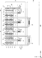
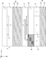
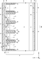
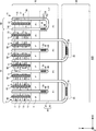
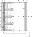
- FIG. 1A shows an example of a top view of the semiconductor device 100.
- the semiconductor device 100 of this example is a semiconductor chip including a transistor unit 70 and a diode unit 80.
- the semiconductor device 100 is a trench gate type RC-IGBT (Reverse Conducting Integrated Gate Bipolar Transistor) in which a plurality of trench portions are arranged.
- the plurality of trench portions are arranged in the X-axis direction and extend in the Y-axis direction.
- the transistor portion 70 is a region in which a collector region 22 provided on the back surface side of the semiconductor substrate 10 is projected onto the upper surface of the semiconductor substrate 10, which will be described later in FIG. 1B.
- the collector region 22 has a second conductive type.
- the collector area 22 of this example is a P + type as an example.
- the transistor unit 70 includes a transistor such as an IGBT.
- the diode portion 80 is a region in which the cathode region 82 provided on the back surface side of the semiconductor substrate 10 is projected onto the upper surface of the semiconductor substrate 10, which will be described later in FIG. 1B.
- the cathode region 82 has a first conductive type.
- the cathode region 82 of this example is N + type as an example.
- the diode section 80 includes a diode such as a freewheeling diode (FWD: Free Wheel Diode) provided adjacent to the transistor section 70 on the upper surface of the semiconductor substrate 10.
- FWD Free Wheel Diode
- FIG. 1A a region around the chip end portion on the edge side of the semiconductor device 100 is shown, and other regions are omitted.
- an edge termination structure portion is provided in a region on the negative side in the Y-axis direction.
- the edge terminal structure portion relaxes the electric field concentration on the upper surface side of the semiconductor substrate 10.
- the edge termination structure has, for example, a guard ring, a field plate, a resurf, and a structure in which these are combined.
- the negative edge in the Y-axis direction will be described, but the same applies to the other edges of the semiconductor device 100.
- the semiconductor substrate 10 may be a silicon substrate, a silicon carbide substrate, a nitride semiconductor substrate such as gallium nitride, or the like.
- the semiconductor substrate 10 of this example is a silicon substrate.
- the semiconductor device 100 of this example has a gate trench portion 40, a dummy trench portion 30, an emitter region 12, a base region 14, a contact region 15, and a well region 17 on the front surface of the semiconductor substrate 10. Be prepared. Further, the semiconductor device 100 of this example includes an emitter electrode 52 and a gate metal layer 50 provided above the front surface of the semiconductor substrate 10.
- the emitter electrode 52 is provided above the gate trench portion 40, the dummy trench portion 30, the emitter region 12, the base region 14, the contact region 15, and the well region 17. Further, the gate metal layer 50 is provided above the gate trench portion 40 and the well region 17.
- the emitter electrode 52 and the gate metal layer 50 are formed of a material containing metal.
- the emitter electrode 52 is formed of an aluminum, aluminum-silicon alloy, or aluminum-silicon-copper alloy.
- At least a partial region of the gate metal layer 50 may be formed of aluminum, aluminum-silicon alloy, or aluminum-silicon-copper alloy.
- the emitter electrode 52 and the gate metal layer 50 may have a barrier metal formed of titanium, a titanium compound, or the like in the lower layer of a region formed of aluminum or the like.
- the emitter electrode 52 and the gate metal layer 50 are provided separately from each other.
- the emitter electrode 52 and the gate metal layer 50 are provided above the semiconductor substrate 10 with the interlayer insulating film 38 interposed therebetween.
- the interlayer insulating film 38 is omitted in FIG. 1A.
- the interlayer insulating film 38 is provided with a contact hole 54, a contact hole 55, and a contact hole 56 penetrating.
- the contact hole 55 connects the gate metal layer 50 and the gate conductive portion in the gate trench portion 40 of the transistor portion 70.
- a plug made of tungsten or the like may be formed inside the contact hole 55.
- the contact hole 56 connects the emitter electrode 52 and the dummy conductive portion in the dummy trench portion 30.
- a plug made of tungsten or the like may be formed inside the contact hole 56.
- connection portion 25 electrically connects the front surface side electrode such as the emitter electrode 52 or the gate metal layer 50 to the semiconductor substrate 10.
- the connecting portion 25 is provided between the gate metal layer 50 and the gate conductive portion.
- the connecting portion 25 is also provided between the emitter electrode 52 and the dummy conductive portion.
- the connecting portion 25 is a conductive material such as polysilicon doped with impurities.
- the connecting portion 25 is polysilicon (N +) doped with N-type impurities.
- the connecting portion 25 is provided above the front surface of the semiconductor substrate 10 via an insulating film such as an oxide film.
- the gate trench portions 40 are arranged at predetermined intervals along a predetermined trench arrangement direction (X-axis direction in this example). As an example, the gate trench portions 40 are arranged at a trench spacing of 1.5 ⁇ m, but the trench spacing is not limited to this spacing.
- the gate trench portion 40 of this example includes two stretching portions 41 that are parallel to the front surface of the semiconductor substrate 10 and stretched along a trench stretching direction (Y-axis direction in this example) perpendicular to the trench arrangement direction. It may have a connecting portion 43 connecting the two stretched portions 41.
- the connecting portion 43 is formed in a curved shape.
- the dummy trench portion 30 of this example is a trench portion that is electrically connected to the emitter electrode 52 and is set to the emitter potential. Similar to the gate trench portion 40, the dummy trench portions 30 are arranged at predetermined intervals along a predetermined trench arrangement direction (in this example, the X-axis direction). As an example, the dummy trench portions 30 are arranged at a trench spacing of 1.5 ⁇ m, but the trench spacing is not limited to this spacing. In particular, the trench spacing of the dummy trench portion 30 may be provided so as to be different from the trench spacing of the gate trench portion 40. Like the gate trench portion 40, the dummy trench portion 30 of this example has a U-shape on the front surface of the semiconductor substrate 10.
- the dummy trench portion 30 may have two stretching portions 31 extending along the trench stretching direction and a connecting portion 33 connecting the two stretching portions 31.
- the dummy trench portion 30 may have a floating potential.
- the dummy trench portion 30 is an example of a first trench portion adjacent to the gate trench portion 40.
- the transistor portion 70 of this example has a structure in which two gate trench portions 40 having a connecting portion 43 and two dummy trench portions 30 having no connecting portion are repeatedly arranged. That is, the arrangement ratio of the gate trench portion 40 and the dummy trench portion 30 may be set to a predetermined desired arrangement ratio. In the transistor portion 70 of this example, the ratio of the number of gate trench portions 40 to the number of dummy trench portions 30 is 1: 1.
- the transistor portion 70 of this example has a dummy trench portion 30 between two extending portions 41 connected by the connecting portion 43.
- the number of gate trench portions 40 may be the number of stretched portions 41.
- the number of dummy trench portions 30 may be the number of stretched portions 31.
- the ratio of the gate trench portion 40 and the dummy trench portion 30 is not limited to this example.
- the ratio of the gate trench portion 40 to the dummy trench portion 30 may be 2: 3 or 2: 4.
- the transistor portion 70 may have a so-called full gate structure in which the dummy trench portion 30 is not provided and all the gate trench portions 40 are used.
- the ratio of the gate trench portion 40 and the dummy trench portion 30 disclosed in the present specification may be read as the ratio of the gate trench portion 40 and the dummy trench.
- the dummy trench includes a trench in which a channel is not formed on the side wall, such as the dummy trench portion 30 or the dummy gate trench portion 130 described later.
- the well region 17 is a second conductive type region provided on the front surface side of the semiconductor substrate 10 with respect to the drift region 18 described later.
- the well region 17 is an example of a well region provided on the edge side of the semiconductor device 100.
- the well region 17 is P + type as an example.
- the well region 17 is formed in a predetermined range from the end of the active region on the side where the gate metal layer 50 is provided.
- the diffusion depth of the well region 17 may be deeper than the depth of the gate trench portion 40 and the dummy trench portion 30.
- a part of the gate trench portion 40 and the dummy trench portion 30 on the gate metal layer 50 side is formed in the well region 17.
- the bottoms of the ends of the gate trench portion 40 and the dummy trench portion 30 in the trench extending direction may be covered with the well region 17.
- the contact hole 54 is formed in the transistor portion 70 above each region of the emitter region 12 and the contact region 15. The emitter region 12 and the contact region 15 are exposed in the contact hole 54.
- the contact holes 54 are not provided above the well regions 17 provided at both ends in the Y-axis direction.
- one or a plurality of contact holes 54 are formed in the interlayer insulating film.
- the one or a plurality of contact holes 54 may be provided by extending in the trench extending direction.
- the mesa portion 71 and the mesa portion 81 are the mesa portions provided adjacent to the trench portion in the plane parallel to the front surface of the semiconductor substrate 10.
- the mesa portion is a portion of the semiconductor substrate 10 sandwiched between two adjacent trench portions, and may be a portion from the front surface of the semiconductor substrate 10 to the depth of the deepest bottom portion in each trench portion. ..
- the extended portion of each trench portion may be used as one trench portion. That is, the region sandwiched between the two stretched portions may be the mesa portion.
- the mesa portion 71 is provided adjacent to at least one of the dummy trench portion 30 or the gate trench portion 40 in the transistor portion 70.
- the mesa portion 71 has a well region 17, an emitter region 12, a base region 14, and a contact region 15 on the front surface of the semiconductor substrate 10.
- the mesa portion 81 is provided adjacent to the dummy trench portion 30 in the diode portion 80.
- the trench portion in the mesa portion 81 may be electrically connected to the emitter electrode 52 through the contact hole 56 and set to the emitter potential. That is, the trench portion provided in the diode portion 80 may be a dummy trench portion 30.
- the mesa portion 81 has a well region 17 and a base region 14 on the front surface of the semiconductor substrate 10.
- the emitter electrode 52 is also arranged on the upper surface of the mesa portion 81. That is, the metal layer of the emitter electrode 52 may function as an anode electrode in the diode portion 80.
- the base region 14 is a second conductive type region provided on the front surface side of the semiconductor substrate 10 in the transistor portion 70.
- the base region 14 is P-type as an example.
- the base region 14 may be provided at both ends of the mesa portion 71 in the Y-axis direction on the front surface 21 of the semiconductor substrate 10. Note that FIG. 1A shows only one end of the base region 14 in the Y-axis direction.
- the emitter region 12 is a first conductive type region having a higher doping concentration than the drift region 18 described later in FIG. 1B.
- the emitter region 12 of this example is N + type as an example.
- the dopant in the emitter region 12 is phosphorus (P), arsenic (As), or the like.
- the emitter region 12 is provided in contact with the gate trench portion 40 on the front surface of the mesa portion 71.
- the emitter region 12 may be provided so as to extend in the X-axis direction from one of the two trench portions sandwiching the mesa portion 71 to the other.
- the emitter region 12 is also provided below the contact hole 54.
- the emitter region 12 may extend to the dummy trench portion 30 and come into contact with the dummy trench portion 30. However, the emitter region 12 may be terminated without reaching the dummy trench portion 30 and may not be in contact with the dummy trench portion 30. The emitter region 12 of this example is not in contact with the dummy trench portion 30.
- the contact region 15 is a second conductive type region having a higher doping concentration than the base region 14.
- the contact region 15 of this example is a P + type as an example.
- An example of a dopant in the contact region 15 is boron (B).
- the contact area 15 of this example is provided on the front surface 21 of the mesa portion 71.
- the contact region 15 may be provided in the X-axis direction from one of the two trench portions sandwiching the mesa portion 71 to the other. However, the contact region 15 may be separated from the gate trench portion 40 below the emitter region 12 at a portion where the emitter region 12 is in contact with the gate trench portion 40.
- the contact area 15 may or may not be in contact with the gate trench portion 40. Further, the contact region 15 may or may not be in contact with the dummy trench portion 30. In this example, the contact region 15 is in contact with the dummy trench portion 30 and the gate trench portion 40. The contact area 15 is also provided below the contact hole 54. The contact region 15 may also be provided in the mesa portion 81.
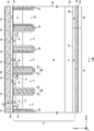
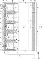
- FIG. 1B is an example of a'a'cross-sectional view in FIG. 1A.
- the aa'cross section is an XZ plane extending from the transistor portion 70 to the diode portion 80 and passing through the emitter region 12 in the transistor portion 70.
- the semiconductor device 100 of this example has a semiconductor substrate 10, an interlayer insulating film 38, an emitter electrode 52, and a collector electrode 24 in the aa'cross section.
- the emitter electrode 52 is formed above the semiconductor substrate 10 and the interlayer insulating film 38.
- the drift region 18 is a first conductive type region provided on the semiconductor substrate 10.
- the drift region 18 of this example is N-type as an example.
- the drift region 18 may be a region remaining in the semiconductor substrate 10 without forming another doping region. That is, the doping concentration of the drift region 18 may be the doping concentration of the semiconductor substrate 10.
- the buffer region 20 is a first conductive type region provided below the drift region 18.
- the buffer area 20 of this example is N-type as an example.
- the doping concentration in the buffer region 20 is higher than the doping concentration in the drift region 18.
- the buffer region 20 may function as a field stop layer that prevents the depletion layer extending from the lower surface side of the base region 14 from reaching the collector region 22 of the second conductive type and the cathode region 82 of the first conductive type.
- the collector area 22 is provided below the buffer area 20 in the transistor unit 70.
- the collector electrode 24 is formed on the back surface 23 of the semiconductor substrate 10.
- the collector electrode 24 is made of a conductive material such as metal.
- the base region 14 is a second conductive type region provided above the drift region 18 in the mesa portion 71 and the mesa portion 81.
- the base region 14 is provided in contact with the gate trench portion 40.
- the base region 14 may be provided in contact with the dummy trench portion 30.
- the emitter region 12 is provided between the base region 14 and the front surface 21 in the mesa portion 71.
- the emitter region 12 is provided in contact with the gate trench portion 40.
- the emitter region 12 may or may not be in contact with the dummy trench portion 30.
- One or more gate trench portions 40 and one or more dummy trench portions 30 are provided on the front surface 21.
- Each trench portion is provided from the front surface 21 to the drift region 18. In the region where at least one of the emitter region 12, the base region 14 and the contact region 15 is provided, each trench portion also penetrates these regions and reaches the drift region 18.
- the fact that the trench portion penetrates the doping region is not limited to those manufactured in the order of forming the doping region and then forming the trench portion. Those in which the doping region is formed between the trench portions after the trench portion is formed are also included in those in which the trench portion penetrates the doping region.
- the gate trench portion 40 has a gate trench formed on the front surface 21, a gate insulating film 42, and a gate conductive portion 44.
- the gate insulating film 42 is formed so as to cover the inner wall of the gate trench.
- the gate insulating film 42 may be formed by oxidizing or nitriding the semiconductor on the inner wall of the gate trench.
- the gate conductive portion 44 is formed inside the gate trench and inside the gate insulating film 42.
- the gate insulating film 42 insulates the gate conductive portion 44 and the semiconductor substrate 10.
- the gate conductive portion 44 is formed of a conductive material such as polysilicon.
- the gate trench portion 40 is covered with an interlayer insulating film 38 on the front surface 21. The potential of a gate electrode such as an IGBT is applied to the gate conductive portion 44.
- the gate conductive portion 44 includes a region facing the adjacent base region 14 on the mesa portion 71 side with the gate insulating film 42 interposed therebetween in the depth direction of the semiconductor substrate 10.
- a predetermined gate voltage is applied to the gate conductive portion 44, a channel due to an electron inversion layer is formed on the surface layer of the interface of the base region 14 in contact with the gate trench.
- the dummy trench portion 30 may have the same structure as the gate trench portion 40.
- the dummy trench portion 30 has a dummy trench formed on the front surface 21 side, a dummy insulating film 32, and a dummy conductive portion 34.
- the dummy insulating film 32 is formed so as to cover the inner wall of the dummy trench.
- the dummy conductive portion 34 is formed inside the dummy trench and inside the dummy insulating film 32.
- the dummy insulating film 32 insulates the dummy conductive portion 34 and the semiconductor substrate 10.
- the dummy trench portion 30 is covered with the interlayer insulating film 38 on the front surface 21.
- the potential of an emitter electrode such as an IGBT is applied to the dummy conductive portion 34.
- the dummy conductive portion 34 may have a floating potential.
- the interlayer insulating film 38 is provided on the front surface 21.
- An emitter electrode 52 is provided above the interlayer insulating film 38.
- the interlayer insulating film 38 is provided with one or a plurality of contact holes 54 for electrically connecting the emitter electrode 52 and the semiconductor substrate 10. Similarly, the contact hole 55 and the contact hole 56 may be provided so as to penetrate the interlayer insulating film 38.
- the lower end 13 is the lower end of the emitter region 12 of the mesa portion 71 on the dummy trench portion 30 side. When the emitter region 12 reaches the dummy trench portion 30, the lower end 13 is in contact with the dummy trench portion 30.
- the contact region 15 is provided below the lower end 13 in the mesa portion 71. That is, the contact region 15 is provided deeper than the emitter region 12 and is provided so as to partially overlap the emitter region 12.
- the contact region 15 of this example is provided so as to extend from the dummy trench portion 30 to below the lower end 13 of the emitter region 12 in the trench arrangement direction. This makes it difficult for holes below the emitter region 12 to be directly extracted through the emitter region 12, and makes it easier for hole currents to be extracted from the contact region 15. This makes it difficult for the NPNP-type parasitic thyristor from the emitter region 12 to the collector region 22 to turn on, and the latch-up of the semiconductor device 100 can be suppressed.
- the contact region 15 is separated from the gate trench portion 40 in the mesa portion 71. As a result, the contact region 15 does not hinder the formation of the inverted layer on the side surface of the gate trench portion 40, and the semiconductor device 100 operates stably.
- the contact region 15 of this example is provided straddling both sides of the dummy trench portion 30 in the X-axis direction.
- a resist is provided on the semiconductor substrate 10, and the contact region 15 that straddles the region where the trench portion is provided can be installed by ion implantation.
- the dummy trench portion 30 can be installed by etching the semiconductor substrate 10 after providing the contact region 15.
- process pitch miniaturization in which the interval between the mesa portions 71 is shortened, has been performed.
- the contact region 15 that extends below the lower end 13 of the emitter region 12 and is separated from the gate trench portion 40 is manufactured. Becomes easier. This makes it possible to provide the semiconductor device 100 having high latch-up resistance without significantly affecting the electrical characteristics.
- the contact region 15 is provided so as to be connected in the trench extending direction, the effect of suppressing latch-up can be realized, and the contact region 15 is not limited to the form in contact with the dummy trench portion 30.
- the buffer region 20 is laminated above the cathode region 82, and the drift region 18 is laminated above the buffer region 20.
- the base region 14 is laminated above the drift region 18, and a PN junction is formed between the base region 14 and the drift region 18.
- the base region 14 is electrically connected to the emitter electrode 52 via the contact hole 54.
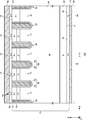
- FIG. 1C is an example of a bb'cross section in FIG. 1A.
- the bb'cross section is an XZ plane that does not pass through the emitter region 12 in the transistor portion 70.
- the mesa portion 71 of the transistor portion 70 has a base region 14 and a contact region 15 above the drift region 18.
- the mesa portion 81 has the same structure as the example in FIG. 1B.
- the contact region 15 extends from the gate trench portion 40 to the dummy trench portion 30.
- a contact hole 54 is provided above the contact area 15. Holes are extracted from the contact region 15 through the contact hole 54.
- the depths of the contact regions 15 are provided at the same depth.
- the contact region 15 is deeper than the emitter region 12.
- the contact region 15 may be provided at different depths below the emitter region 12 and in other regions.
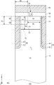
- FIG. 2 shows an example of an enlarged cross-sectional view of the mesa portion 71.
- the transistor portion 70 the XZ plane passing through the emitter region 12 is shown.
- the emitter region 12 extends from the gate trench portion 40 to the dummy trench portion 30 beyond the contact hole 54 in the trench arrangement direction. As a result, the current easily conducts from the emitter region 12 through the contact hole 54, and the electrical characteristics of the semiconductor device 100 are improved.
- the emitter region 12 of this example extends from the gate trench portion 40 to the dummy trench portion 30 in the trench arrangement direction, and terminates without reaching the dummy trench portion 30.
- the emitter region 12 may be provided extending from the gate trench portion 40 to the dummy trench portion 30 in the trench arrangement direction.
- the contact region 15 is provided on the front surface 21 of the semiconductor substrate 10 on the side wall of the dummy trench portion 30.
- the contact region 15 includes a surface region 92 and a lower region 94.
- the surface region 92 is a region of the semiconductor substrate 10 having the same depth as the emitter region 12. As an example, the depth of the surface region 92 is 0.5 ⁇ m. However, the depth of the surface region 92 may be different.
- the impurity concentration in the surface region 92 may be in the range of 5E19 / cm3 or more and 2E20 / cm3 or less.
- the lower region 94 is provided in a region deeper than the emitter region 12 in the semiconductor substrate 10.
- the lower region 94 extends beyond the lower end 13 of the emitter region 12 on the gate trench portion 40 side extending from the gate trench portion 40 to the dummy trench portion 30 toward the gate trench portion 40.
- the impurity concentration in the lower region 94 may be in the range of 1E19 / cm3 or more and 1E20 / cm3 or less.
- the width Wc is the width of the contact region 15 in the trench arrangement direction.
- the width Wc is a width measured from the center of the dummy trench portion 30 to the lower end of the emitter region 12 on the dummy trench portion 30 side. That is, the width Wc corresponds to the maximum reach position on the gate trench portion 40 side of the lower region 94 measured from the center of the dummy trench portion 30.
- the width Wc may be 1.2 ⁇ m or less, and may be 1.1 ⁇ m or less.
- the width of the surface region 92 in the trench arrangement direction may be in the range of 15% or more and 40% or less with respect to the distance between adjacent trenches.
- the width of the lower region 94 in the trench arrangement direction may be in the range of 30% or more and 70% or less with respect to the distance between adjacent trenches.
- the width of the portion where the lower region 94 overlaps the emitter region 12 in the trench arrangement direction may be in the range of 0% or more and 30% or less with respect to the distance between adjacent trenches, and more preferably 10% or more and 20. It may be in the range of% or less.
- the thickness Dc is the thickness of the contact region 15 in the depth direction of the semiconductor substrate 10.
- the thickness Dc is thicker than the depth of the lower end 13 of the emitter region 12 and less than the depth of the base region 14.
- the thickness Dc is 0.5 ⁇ m or more and 2.0 ⁇ m or less.
- the thickness of the surface region 92 may be in the range of 0.3 ⁇ m or more and 0.8 ⁇ m or less.
- the thickness of the lower region 94 may be in the range of 0.3 ⁇ m or more and 1.1 ⁇ m or less.
- the width Ws is the distance between the contact region 15 and the gate trench portion 40 in the trench arrangement direction.
- a width Ws may be provided so that a channel can be formed at the end of the gate trench 40. That is, the width Ws corresponds to the separation distance between the contact region 15 and the gate trench portion 40.
- the width Ws is 0.6 ⁇ m or more.
- the width Ws in the trench arrangement direction may be in the range of 30% or more and 70% or less with respect to the distance between adjacent trenches.
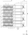
- FIG. 3 shows an example of a top view of the semiconductor device 100 having an unopened portion of the contact hole 54.
- FIG. 3 is an example of an enlarged view of the upper surface of the semiconductor device 100.
- the non-connection region 59 is a region in which the emitter electrode 52 is not electrically connected to the contact region 15 on the front surface 21.
- the non-connecting region 59 is an unopened region in which the contact hole 54 is not formed in the interlayer insulating film 38 due to poor etching of the oxide film caused by particles, foreign matter, or the like.
- the non-connection region 59 may be a region in which the contact region 15 of the front surface 21 is not formed due to the residue of resist or the like.
- the hole current that was supposed to be drawn in the non-connection region 59 flows through the contact region 15 and is pulled out through the contact hole 54 above the other neighboring contact region 15. That is, since the hole current does not flow through the base region 14 below the emitter region 12 but flows through the contact region 15 which has a lower resistance to holes than the base region 14, latch-up can be suppressed. As a result, switching failure due to process defects is suppressed. Therefore, the semiconductor device 100 having an element structure having a strong redundancy against process defects is provided.
- FIG. 4A shows an example of the simulation result of the static characteristics of the semiconductor device 100.
- the change in static characteristics with respect to the width Wc of the contact region 15 is shown.
- an example is shown in which the width of the mesa portion 71 between the dummy trench portion 30 and the gate trench portion 40 is 1.5 ⁇ m.
- the unit of each standardized value may be an appropriate unit having a dimension corresponding to each physical quantity.
- the relationship between the voltage and Vth is shown.
- FIG. 4B shows an example of the simulation result of the on-characteristics of the semiconductor device 100.
- the change of the on characteristic with respect to the width Wc of the contact region 15 is shown.
- the numerical value on the vertical axis of this example is scaled to a normalized value.
- the relationship between the maximum value di / dt_max (Normalized) of the time change and the relationship between the on-loss Eon (Normalized) of the semiconductor device 100 is shown.
- the width Wc is 1.2 ⁇ m or less, the influence of the contact region 15 on the channel formation of the base region 14 is small. Therefore, when the width Wc is in this range, the influence on all these on-characteristic values can be maintained in a small range.
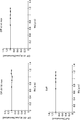
- FIG. 4C shows an example of the simulation result of the off characteristic of the semiconductor device 100.
- the change of the off characteristic with respect to the width Wc of the contact region 15 is shown.
- the numerical value on the vertical axis of this example is scaled to a normalized value.
- the relationship between the maximum value di / dt_max (Normalized) of the time change and the relationship between the on-loss Off (Normalized) of the semiconductor device 100 is shown.
- the width Wc is 1.2 ⁇ m or less, the influence of the contact region 15 on the channel formation of the base region 14 is small. Therefore, when the width Wc is in this range, the influence on all these off characteristic values can be maintained in a small range.
- the semiconductor device 100 of this example does not affect the dynamic electrical characteristics due to the structure of the contact region 15. Therefore, as shown in the simulation results of FIGS. 4A to 4C, the semiconductor device 100 of this example does not significantly affect the electrical characteristics in terms of both static characteristics and dynamic characteristics.
- the semiconductor device 100 of this example improves the latch-up withstand without changing the electrical characteristics.
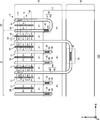
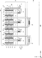
- FIG. 5A shows an example of a top view of the semiconductor device 100. This example differs from FIG. 1A in that the emitter region 12 is provided in contact with the dummy trench portion 30. In this example, the differences from FIG. 1A will be particularly described.
- the emitter region 12 of this example extends from the gate trench portion 40 to the dummy trench portion 30 in the trench arrangement direction.
- the emitter region 12 and the contact region 15 are provided on the front surface 21 of the semiconductor substrate 10 in alternating contact with each of the gate trench portion 40 and the dummy trench portion 30 in the trench extending direction.
- FIG. 5B is an example of a cross-sectional view taken along the line cc'in FIG. 5A.
- the cc'cross section is an XZ plane extending from the transistor portion 70 to the diode portion 80 and passing through the emitter region 12 in the transistor portion 70.
- the XZ cross section extending from the transistor portion 70 to the diode portion 80 and passing through the contact region 15 in the transistor portion 70 is the same as that in FIG. 1C.
- the surface region 92 of the contact region 15 is not provided in the cc'cross section.
- the contact region 15 of this example has a structure similar to that of the example of FIG. 1B in the lower region 94. That is, at least a part of the contact region 15 is provided below the lower end 13 in the mesa portion 71. As a result, it becomes difficult for holes below the emitter region 12 to be directly extracted through the emitter region 12, and the hole current can be extracted from the contact region 15 to suppress latch-up.
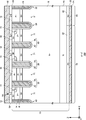
- FIG. 6A shows an example of a top view of the semiconductor device 100.
- the ratio of the number of gate trench portions 40 to the number of dummy trench portions 30 is 1: 2.
- the resistance to defects can be improved by increasing the ratio of the dummy trench portion 30.
- a gate trench portion 40 having a U-shaped structure and two dummy trench portions 30 having an I-shaped structure are arranged.
- the structures of the gate trench portion 40 and the dummy trench portion 30 are not limited to these as long as the arrangement ratio of the gate trench portion 40 and the dummy trench portion 30 can be maintained at 1: 2.
- the dummy trench portion 30 has a U-shaped structure, and the region inside the dummy trench portion may be a floating region.
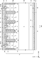
- FIG. 6B is an example of a cross-sectional view taken along the line dd'in FIG. 6A.
- the dd'cross section is an XZ plane extending from the transistor portion 70 to the diode portion 80 and passing through the emitter region 12 in the transistor portion 70.
- the semiconductor device 100 of this example has a semiconductor substrate 10, an interlayer insulating film 38, an emitter electrode 52, and a collector electrode 24 in a dd'cross section.
- the emitter electrode 52 is formed above the semiconductor substrate 10 and the interlayer insulating film 38.
- the semiconductor device 100 of this example has a storage region 16 between the drift region 18 and the base region 14.
- the storage region 16 is a first conductive type region provided between the base region 14 and the drift region 18.
- the storage area 16 of this example is N + type as an example.
- the storage region 16 is provided in the transistor portion 70 and the diode portion 80. As a result, the semiconductor device 100 can avoid the mask shift of the storage region 16.
- the storage area 16 is provided in contact with the gate trench portion 40.
- the storage region 16 may or may not be in contact with the dummy trench portion 30.
- the doping concentration of the accumulation region 16 is higher than the doping concentration of the drift region 18.
- the dose amount of ion implantation in the accumulation region 16 may be 1E12 cm-2 or more and 1E13 cm- 2 or less. Further, the ion implantation dose amount of the accumulation region 16 may be 3E12 cm-2 or more and 6E12 cm- 2 or less.
- E is meant a power of 10, for example, 1E12 cm -2 refers to 1 ⁇ 10 12 cm -2.
- the contact region 15 electrically connects the contact region 15 below the emitter region 12.
- the semiconductor device 100 can suppress latch-up due to the structure of the contact region 15 regardless of the presence or absence of the storage region 16 and the arrangement ratio of the gate trench portion 40 and the dummy trench portion 30.
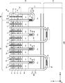
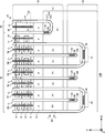
- FIG. 7A shows an example of a top view of the semiconductor device 100, which is a modified example.
- the semiconductor device 100 of this example includes a dummy gate trench portion 130 that does not come into contact with the emitter region 12 instead of the dummy trench portion 30.
- the dummy gate trench portion 130 is an example of a first trench portion adjacent to the gate trench portion 40.
- the dummy gate trench portion 130 is a trench portion that is set to the gate potential and does not come into contact with the emitter region 12. That is, the dummy gate trench portion 130 is a trench portion that is set to the gate potential but does not drive the transistor in the adjacent mesa portion 71, and is an example of a dummy trench portion different from the dummy trench portion 30. In order to set the dummy gate trench portion 130 to the gate potential, the dummy gate trench portion 130 extends in the Y-axis direction to the region where the gate metal layer 50 is provided. The dummy gate trench portion 130 is connected to the gate metal layer 50 via the contact hole 58 and is set to the gate potential.
- the dummy gate trench portion 130 is set to the gate potential, it is not in contact with the emitter region 12, so that a channel due to the first conductive type inversion layer is not formed on the side wall of the dummy gate trench portion 130. Since the dummy gate trench portion 130 makes it easier to attract the carrier to the mesa portion 71, the properties such as the gate capacity are different from those of the dummy gate trench portion 130. Therefore, by using the dummy gate trench portion 130 and the dummy trench portion 30 in combination, it is possible to adjust the threshold voltage, saturation current, electric field concentration, gate capacitance, etc. in the semiconductor device 100.
- the gate trench portion 40 of this example has a U-shaped structure, and the dummy gate trench portion 130 has an I-shaped structure.
- the structures of the gate trench portion 40 and the dummy gate trench portion 130 are not limited to these structures as long as the desired arrangement ratio can be achieved.
- the dummy gate trench portion 130 in the diode portion 80 has the same structure as that of FIG. 1A. That is, the dummy gate trench portion 130 is connected to the emitter electrode 52 via the contact hole 56 and is set to the emitter potential.
- FIG. 7B is an example of a cross-sectional view taken along the line ee'in FIG. 7A.
- the ee'cross section is an XZ plane extending from the transistor portion 70 to the diode portion 80 and passing through the emitter region 12 in the transistor portion 70.
- the dummy gate trench portion 130 has a second gate insulating film 132 and a second gate conductive portion 134.
- the dummy gate trench portion 130 of the semiconductor device 100 has the same configuration as the cross-sectional view in FIG. 1B, except that the dummy gate trench portion 130 has an emitter potential. That is, also in this example, the contact region 15 electrically connects the contact region 15 below the emitter region 12. Therefore, the semiconductor device 100 can suppress latch-up due to the structure of the contact region 15 regardless of the potential of the dummy gate trench portion.
- FIG. 8A shows an example of a top view of the semiconductor device 100.
- the semiconductor device 100 of this example includes a contact trench portion 60.
- the contact trench portion 60 is provided so as to extend from the front surface 21 in the depth direction of the semiconductor substrate 10.
- the contact trench portion 60 electrically connects the emitter electrode 52 and the semiconductor substrate 10.
- the contact trench portion 60 is provided so as to extend in the trench extending direction.
- the contact trench portion 60 of this example is arranged in a stripe shape along the gate trench portion 40 and the dummy trench portion 30.
- the contact trench portion 60 is formed in the transistor portion 70 above each region of the emitter region 12 and the contact region 15.
- the contact trench portion 60 is formed in the diode portion 80 above the region of the base region 14.
- the contact trench portion 60 is not provided above the well regions 17 provided at both ends in the Y-axis direction.
- the one or a plurality of contact trench portions 60 may be provided so as to extend in the trench extending direction.
- the emitter region 12 and the contact region 15 may be alternately arranged in the trench extending direction.
- the width of the emitter region 12 may be larger than the width of the contact region 15.
- the width of the emitter region 12 in the trench stretching direction may be 0.6 ⁇ m or more and 1.6 ⁇ m or less.
- FIG. 8B is an example of a cross-sectional view taken along the line ff in FIG. 8A.
- the contact trench portion 60 of this example is formed shallower than the emitter region 12.
- the contact trench portion 60 is provided so as to extend from the front surface 21 to the back surface 23 side of the semiconductor substrate 10.
- the lower end of the contact trench portion 60 of this example is shallower than the lower end of the emitter region 12.
- Emitter regions 12 are provided at both ends of the contact trench portion 60 in the trench arrangement direction.
- the contact trench portion 60 has a plug 62 and a barrier metal layer 64.
- the plug 62 is a conductive material provided inside the contact trench portion 60.
- the plug 62 may be made of the same material as the emitter electrode 52 or may be made of a different material.
- the plug 62 may contain a material such as tungsten.
- the barrier metal layer 64 is provided below the plug 62.
- the barrier metal layer 64 of this example is provided between the plug 62 and the emitter region 12.
- the barrier metal layer 64 may contain a material such as titanium nitride.
- the emitter region 12 is provided in contact with the gate trench portion 40.
- the emitter region 12 may or may not be in contact with the dummy trench portion 30.
- the emitter region 12 of this example is provided so as to extend toward the dummy trench portion 30 with respect to the contact trench portion 60 in the trench arrangement direction. That is, the lower end 13 is provided between the dummy trench portion 30 and the contact trench portion 60 in the trench arrangement direction.
- At least a part of the contact area 15 is provided below the lower end 13 in the mesa portion 71.
- the contact region 15 of this example is provided so as to extend from the dummy trench portion 30 to below the lower end 13 of the emitter region 12 in the trench arrangement direction.
- the contact region 15 may or may not extend beyond the contact trench portion 60 from the dummy trench portion 30 in the trench arrangement direction.
- the contact region 15 of this example is provided between the dummy trench portion 30 and the contact trench portion 60 in the trench arrangement direction.
- the trench bottom region 19 is a second conductive type region provided below the dummy trench portion 30 and the gate trench portion 40.
- the trench bottom region 19 of this example covers the lower ends of the dummy trench portion 30 and the gate trench portion 40.
- the doping concentration of the trench bottom region 19 may be smaller than that of the base region 14.
- the trench bottom region 19 is provided between the drift region 18a and the drift region 18b. By providing the trench bottom region 19, the avalanche withstand capacity is improved.
- the trench bottom region 19 may be omitted.
- the drift region 18a is provided between the base region 14 and the trench bottom region 19 in the mesa portion 71 and the mesa portion 81.
- the drift region 18b is provided below the trench bottom region 19.
- the doping concentrations of the drift region 18a and the drift region 18b may be the same.
- FIG. 9A shows an example of a top view of the semiconductor device 100.
- the arrangement of the emitter region 12 and the contact region 15 on the front surface 21 is different from that of the embodiment of FIG. 8A.
- the differences from the embodiment of FIG. 8A will be specifically described.
- This example differs from the embodiment of FIG. 8A in that the emitter region 12 is provided on one side of the contact trench portion 60.
- the emitter region 12 is provided in contact with the gate trench portion 40.
- the emitter region 12 is provided so as to extend from the gate trench portion 40 to the side wall of the contact trench portion 60 in the trench arrangement direction.
- the emitter region 12 does not have to be provided between the dummy trench portion 30 and the contact trench portion 60.
- FIG. 9B is an example of a cross-sectional view taken along the line gg'in FIG. 9A.
- the contact trench portion 60 of this example is formed deeper than the embodiment of FIG. 8B.
- the contact trench portion 60 is provided so as to extend from the emitter region 12 to the back surface 23 side of the semiconductor substrate 10. That is, the lower end of the contact trench portion 60 of this example is deeper than the lower end of the emitter region 12. The lower end of the contact trench portion 60 of this example is shallower than the lower end of the contact region 15.
- the emitter region 12 is provided so as to extend from the gate trench portion 40 to the side wall of the contact trench portion 60 in the trench arrangement direction. Therefore, the lower end 13 is located between the gate trench portion 40 and the contact trench portion 60 and on the side wall of the contact trench portion 60 in the trench arrangement direction.
- FIG. 10A shows an example of a top view of the semiconductor device 100.
- the semiconductor device 100 of this example differs from the embodiment of FIG. 8A in that it does not include the diode portion 80.
- FIG. 10B is an example of a cross-sectional view taken along the line h-h'in FIG. 10A.
- the contact trench portion 60 of this example is formed deeper than the embodiment of FIG. 8B.
- the contact trench portion 60 is provided so as to extend from the emitter region 12 to the back surface 23 side of the semiconductor substrate 10.
- the lower end of the contact trench portion 60 of this example is deeper than the lower end of the emitter region 12 and shallower than the lower end of the contact region 15.
- Emitter regions 12 are provided at both ends of the contact trench portion 60 in the trench arrangement direction.
- the emitter region 12 is provided so as to extend toward the dummy trench portion 30 from the contact trench portion 60 in the trench arrangement direction. That is, the lower end 13 is provided between the dummy trench portion 30 and the contact trench portion 60 in the trench arrangement direction.
- FIG. 10C is another example of the hh'cross section in FIG. 10A.
- the depth of the contact trench portion 60 is different from that of the embodiment of FIG. 10B.
- the contact trench portion 60 of this example is formed shallower than the emitter region 12. That is, the lower end of the contact trench portion 60 of this example is shallower than the lower end of the emitter region 12.
- the depth of the contact trench portion 60 is not limited to the embodiment and may be appropriately changed. Further, the emitter region 12 may be provided at both ends of the contact trench portion 60 in the trench arrangement direction, or may be provided on one side. Further, in each embodiment, the semiconductor device 100 may or may not include the trench bottom region 19.
- FIG. 11A shows an example of a top view of the semiconductor device 100.
- the semiconductor device 100 of this example includes a dummy gate trench portion 30 provided adjacent to the gate trench portion 40 and a dummy gate trench portion 130 provided adjacent to the gate trench portion 40.
- the dummy gate trench portion 130 is a trench portion that is set to the gate potential and does not come into contact with the emitter region 12.
- the dummy gate trench portion 130 of this example is connected to the extending portion 41 by the connecting portion 43.
- the emitter region 12 is provided in contact with the gate trench portion 40 and separated from the dummy gate trench portion 130 in the mesa portion 71 between the gate trench portion 40 and the dummy gate trench portion 130.
- the emitter region 12 is provided in contact with the gate trench portion 40 in the mesa portion 71 between the gate trench portion 40 and the dummy trench portion 30 and separated from the dummy trench portion 30.
- FIG. 11B is an example of a cross-sectional view taken along the line i-i'in FIG. 11A.
- the semiconductor device 100 of this example includes, but is not limited to, a contact trench portion 60 shallower than the emitter region 12 and emitter regions 12 provided at both ends of the contact trench portion 60 in the trench arrangement direction.
- the dummy gate trench portion 130 is a dummy trench like the dummy trench portion 30. Therefore, a part of the dummy gate trench portion 130 may be replaced with the dummy trench portion 30 having an emitter potential. As a result, the gate capacitance can be adjusted, so that the optimum switching speed can be realized.
- the contact region 15 is provided below the lower end 13 of the emitter region 12 on the dummy gate trench portion 130 side in the mesa portion 71 between the gate trench portion 40 and the dummy gate trench portion 130. Further, the contact region 15 is provided below the lower end 13 on the dummy trench portion 30 side of the emitter region 12 in the mesa portion 71 between the gate trench portion 40 and the dummy trench portion 30.
- FIG. 12A shows an example of a top view of the semiconductor device 100.
- the semiconductor device 100 of this example is different from the embodiment of FIG. 11A in that the first trench portion adjacent to the gate trench portion 40 is the gate trench portion 40 and has a staggered structure.
- the semiconductor device 100 has a plurality of gate trench portions 40 provided adjacent to each other.
- a plurality of gate trench portions 40 provided adjacent to each other may be connected to each other by a connecting portion 43.
- a plurality of gate trench portions 40 provided adjacent to each other are in contact with the emitter region 12 at different positions in the trench extending direction. That is, the semiconductor device 100 has a staggered structure and includes emitter regions 12 arranged in a staggered manner.
- each of the adjacent gate trench portions 40 has both a portion to be a gate trench portion and a portion to be a first trench portion. That is, in the mesa portion between the adjacent gate trench portions 40, the emitter region 12 (first emitter region) that is in contact with one gate trench portion 40 and is separated from the other gate trench portion 40, and one gate trench portion 40. It has an emitter region 12 (second emitter region) which is separated from the ground and is in contact with the other gate trench portion 40.
- the contact region 15 is provided in a region including the lower end 13 on the other gate trench portion 40 side of the first emitter region and the lower end 13 on the one gate trench portion 40 side of the second emitter region. .. Further, in the trench extending direction of the gate trench portion 40, the first emitter region and the second emitter region are alternately provided with the contact region 15 interposed therebetween.
- FIG. 12B is an example of a cross-sectional view taken along the line jj'in FIG. 12A.
- the semiconductor device 100 of this example includes, but is not limited to, a contact trench portion 60 shallower than the emitter region 12 and emitter regions 12 provided at both ends of the contact trench portion 60 in the trench arrangement direction. That is, the semiconductor device 100 may include a contact trench portion 60 deeper than the emitter region 12, or may include an emitter region 12 provided on one side of the contact trench portion 60.
- the semiconductor device 100 may or may not include the trench bottom region 19.
- FIG. 13A shows an example of a top view of the semiconductor device 100.
- the semiconductor device 100 of this example is different from the embodiment of FIG. 12A in that the dummy trench portion 30 is not provided and only the gate trench portion 40 is provided.
- the semiconductor device 100 of this example has a staggered structure in which the emitter regions 12 are alternately arranged, as in the embodiment of FIG. 12A.
- the ratio of the emitter region 12 on the front surface 21 is larger than that of the embodiment of FIG. 12A.
- the semiconductor device 100 of this example even when the ratio of the emitter region 12 on the front surface 21 is increased, a part of the emitter region 12 is separated from the gate trench portion 40, so that the semiconductor device 100 is of the semiconductor device 100. Latch-up can be suppressed.
- FIG. 13B is an example of a kk'cross section in FIG. 13A.
- the semiconductor device 100 of this example includes, but is not limited to, a contact trench portion 60 shallower than the emitter region 12 and emitter regions 12 provided at both ends of the contact trench portion 60 in the trench arrangement direction.
- the emitter region 12 of this example is provided at both ends of the gate trench portion 40 in the trench arrangement direction. In this case, by patterning the adjacent emitter regions 12 together with the gate trench portion 40 interposed therebetween, the reliability of the process can be maintained even when the mesa width becomes small.
Landscapes
- Electrodes Of Semiconductors (AREA)
- Metal-Oxide And Bipolar Metal-Oxide Semiconductor Integrated Circuits (AREA)
Priority Applications (6)
| Application Number | Priority Date | Filing Date | Title |
|---|---|---|---|
| DE112021000202.3T DE112021000202T5 (de) | 2020-07-03 | 2021-04-01 | Halbleitervorrichtung |
| JP2022533692A JP7327672B2 (ja) | 2020-07-03 | 2021-04-01 | 半導体装置 |
| CN202180007468.1A CN114846622A (zh) | 2020-07-03 | 2021-04-01 | 半导体装置 |
| US17/847,167 US20220328669A1 (en) | 2020-07-03 | 2022-06-23 | Semiconductor device |
| JP2023123888A JP7726248B2 (ja) | 2020-07-03 | 2023-07-28 | 半導体装置 |
| JP2025127679A JP2025160397A (ja) | 2020-07-03 | 2025-07-30 | 半導体装置 |
Applications Claiming Priority (2)
| Application Number | Priority Date | Filing Date | Title |
|---|---|---|---|
| JP2020-115759 | 2020-07-03 | ||
| JP2020115759 | 2020-07-03 |
Related Child Applications (1)
| Application Number | Title | Priority Date | Filing Date |
|---|---|---|---|
| US17/847,167 Continuation US20220328669A1 (en) | 2020-07-03 | 2022-06-23 | Semiconductor device |
Publications (1)
| Publication Number | Publication Date |
|---|---|
| WO2022004084A1 true WO2022004084A1 (ja) | 2022-01-06 |
Family
ID=79315725
Family Applications (1)
| Application Number | Title | Priority Date | Filing Date |
|---|---|---|---|
| PCT/JP2021/014138 Ceased WO2022004084A1 (ja) | 2020-07-03 | 2021-04-01 | 半導体装置 |
Country Status (5)
| Country | Link |
|---|---|
| US (1) | US20220328669A1 (https=) |
| JP (3) | JP7327672B2 (https=) |
| CN (1) | CN114846622A (https=) |
| DE (1) | DE112021000202T5 (https=) |
| WO (1) | WO2022004084A1 (https=) |
Cited By (4)
| Publication number | Priority date | Publication date | Assignee | Title |
|---|---|---|---|---|
| JP2023113080A (ja) * | 2022-02-02 | 2023-08-15 | 富士電機株式会社 | 半導体装置および半導体装置の製造方法 |
| JP2024009540A (ja) * | 2022-07-11 | 2024-01-23 | 富士電機株式会社 | 半導体装置 |
| WO2024241741A1 (ja) * | 2023-05-23 | 2024-11-28 | 富士電機株式会社 | 半導体装置および半導体装置の製造方法 |
| WO2026058816A1 (ja) * | 2024-09-12 | 2026-03-19 | ローム株式会社 | 半導体装置 |
Families Citing this family (7)
| Publication number | Priority date | Publication date | Assignee | Title |
|---|---|---|---|---|
| US11276686B2 (en) * | 2019-05-15 | 2022-03-15 | Fuji Electric Co., Ltd. | Semiconductor device |
| WO2021254615A1 (en) * | 2020-06-18 | 2021-12-23 | Dynex Semiconductor Limited | Reverse conducting igbt with controlled anode injection |
| JP7456520B2 (ja) * | 2020-12-07 | 2024-03-27 | 富士電機株式会社 | 半導体装置 |
| KR20230150663A (ko) * | 2022-04-22 | 2023-10-31 | 현대모비스 주식회사 | 전력 반도체 소자, 이를 포함하는 전력 반도체 칩 및 이의 제조 방법 |
| JP2024097277A (ja) * | 2023-01-05 | 2024-07-18 | 富士電機株式会社 | 半導体装置 |
| CN117497574B (zh) * | 2023-08-31 | 2024-05-14 | 海信家电集团股份有限公司 | 半导体装置 |
| WO2025170006A1 (ja) * | 2024-02-09 | 2025-08-14 | 富士電機株式会社 | 半導体装置 |
Citations (4)
| Publication number | Priority date | Publication date | Assignee | Title |
|---|---|---|---|---|
| JP2012178389A (ja) * | 2011-02-25 | 2012-09-13 | Renesas Electronics Corp | 半導体装置 |
| JP2018195798A (ja) * | 2017-05-16 | 2018-12-06 | 富士電機株式会社 | 半導体装置 |
| JP2019016802A (ja) * | 2015-02-03 | 2019-01-31 | 富士電機株式会社 | 半導体装置及びその製造方法 |
| JP2019195093A (ja) * | 2016-03-10 | 2019-11-07 | 富士電機株式会社 | 半導体装置 |
Family Cites Families (20)
| Publication number | Priority date | Publication date | Assignee | Title |
|---|---|---|---|---|
| FR2703831A1 (fr) * | 1993-04-07 | 1994-10-14 | Philips Composants | Dispositif semiconducteur comprenant un transistor latéral. |
| JP2009283540A (ja) | 2008-05-20 | 2009-12-03 | Denso Corp | 炭化珪素半導体装置およびその製造方法 |
| WO2009154882A2 (en) | 2008-06-20 | 2009-12-23 | Maxpower Semiconductor Inc. | Semiconductor power switches having trench gates |
| WO2012006261A2 (en) | 2010-07-06 | 2012-01-12 | Maxpower Semiconductor Inc. | Power semiconductor devices, structures, and related methods |
| JP6190206B2 (ja) * | 2012-08-21 | 2017-08-30 | ローム株式会社 | 半導体装置 |
| JP6440989B2 (ja) * | 2013-08-28 | 2018-12-19 | ローム株式会社 | 半導体装置 |
| US9960165B2 (en) * | 2013-11-05 | 2018-05-01 | Toyota Jidosha Kabushiki Kaisha | Semiconductor device having adjacent IGBT and diode regions with a shifted boundary plane between a collector region and a cathode region |
| DE102014117780B4 (de) * | 2014-12-03 | 2018-06-21 | Infineon Technologies Ag | Halbleiterbauelement mit einer Grabenelektrode und Verfahren zur Herstellung |
| JP6817777B2 (ja) | 2015-12-16 | 2021-01-20 | ローム株式会社 | 半導体装置 |
| JP6885101B2 (ja) * | 2016-03-11 | 2021-06-09 | 富士電機株式会社 | 半導体装置 |
| JP6854598B2 (ja) * | 2016-07-06 | 2021-04-07 | ローム株式会社 | 半導体装置 |
| CN108780814B (zh) | 2016-09-14 | 2021-12-21 | 富士电机株式会社 | 半导体装置及其制造方法 |
| JP6958011B2 (ja) * | 2017-06-15 | 2021-11-02 | 富士電機株式会社 | 半導体装置および半導体装置の製造方法 |
| CN109256417B (zh) * | 2017-07-14 | 2023-10-24 | 富士电机株式会社 | 半导体装置 |
| JP7143575B2 (ja) * | 2017-07-18 | 2022-09-29 | 富士電機株式会社 | 半導体装置 |
| JP6958093B2 (ja) * | 2017-08-09 | 2021-11-02 | 富士電機株式会社 | 半導体装置 |
| CN109524396B (zh) * | 2017-09-20 | 2023-05-12 | 株式会社东芝 | 半导体装置 |
| JP7151076B2 (ja) * | 2017-12-11 | 2022-10-12 | 富士電機株式会社 | 絶縁ゲート型半導体装置 |
| CN111033751B (zh) * | 2018-02-14 | 2023-08-18 | 富士电机株式会社 | 半导体装置 |
| JP6984732B2 (ja) * | 2018-03-15 | 2021-12-22 | 富士電機株式会社 | 半導体装置 |
-
2021
- 2021-04-01 JP JP2022533692A patent/JP7327672B2/ja active Active
- 2021-04-01 CN CN202180007468.1A patent/CN114846622A/zh active Pending
- 2021-04-01 DE DE112021000202.3T patent/DE112021000202T5/de active Pending
- 2021-04-01 WO PCT/JP2021/014138 patent/WO2022004084A1/ja not_active Ceased
-
2022
- 2022-06-23 US US17/847,167 patent/US20220328669A1/en active Pending
-
2023
- 2023-07-28 JP JP2023123888A patent/JP7726248B2/ja active Active
-
2025
- 2025-07-30 JP JP2025127679A patent/JP2025160397A/ja active Pending
Patent Citations (4)
| Publication number | Priority date | Publication date | Assignee | Title |
|---|---|---|---|---|
| JP2012178389A (ja) * | 2011-02-25 | 2012-09-13 | Renesas Electronics Corp | 半導体装置 |
| JP2019016802A (ja) * | 2015-02-03 | 2019-01-31 | 富士電機株式会社 | 半導体装置及びその製造方法 |
| JP2019195093A (ja) * | 2016-03-10 | 2019-11-07 | 富士電機株式会社 | 半導体装置 |
| JP2018195798A (ja) * | 2017-05-16 | 2018-12-06 | 富士電機株式会社 | 半導体装置 |
Cited By (5)
| Publication number | Priority date | Publication date | Assignee | Title |
|---|---|---|---|---|
| JP2023113080A (ja) * | 2022-02-02 | 2023-08-15 | 富士電機株式会社 | 半導体装置および半導体装置の製造方法 |
| US12439622B2 (en) | 2022-02-02 | 2025-10-07 | Fuji Electric Co., Ltd. | Semiconductor device and manufacturing method of semiconductor device |
| JP2024009540A (ja) * | 2022-07-11 | 2024-01-23 | 富士電機株式会社 | 半導体装置 |
| WO2024241741A1 (ja) * | 2023-05-23 | 2024-11-28 | 富士電機株式会社 | 半導体装置および半導体装置の製造方法 |
| WO2026058816A1 (ja) * | 2024-09-12 | 2026-03-19 | ローム株式会社 | 半導体装置 |
Also Published As
| Publication number | Publication date |
|---|---|
| JP7726248B2 (ja) | 2025-08-20 |
| JPWO2022004084A1 (https=) | 2022-01-06 |
| US20220328669A1 (en) | 2022-10-13 |
| JP7327672B2 (ja) | 2023-08-16 |
| CN114846622A (zh) | 2022-08-02 |
| JP2025160397A (ja) | 2025-10-22 |
| JP2023139265A (ja) | 2023-10-03 |
| DE112021000202T5 (de) | 2022-08-18 |
Similar Documents
| Publication | Publication Date | Title |
|---|---|---|
| JP7327672B2 (ja) | 半導体装置 | |
| CN109891595B (zh) | 半导体装置 | |
| JP7666650B2 (ja) | 半導体装置 | |
| CN111033751B (zh) | 半导体装置 | |
| JP2020077674A (ja) | 半導体装置および製造方法 | |
| JP7803330B2 (ja) | 半導体装置および半導体装置の製造方法 | |
| US10916628B2 (en) | Semiconductor device | |
| CN110692140A (zh) | 半导体装置 | |
| JP2021073714A (ja) | 半導体装置およびその製造方法 | |
| JPWO2019159657A1 (ja) | 半導体装置 | |
| JP6958011B2 (ja) | 半導体装置および半導体装置の製造方法 | |
| WO2018147466A1 (ja) | 半導体装置 | |
| US20140084333A1 (en) | Power semiconductor device | |
| JP2002353452A (ja) | 電力用半導体素子 | |
| JP2018152426A (ja) | 半導体装置 | |
| US12439622B2 (en) | Semiconductor device and manufacturing method of semiconductor device | |
| US20240088221A1 (en) | Semiconductor device | |
| CN107833915A (zh) | 半导体器件 | |
| JP7732510B2 (ja) | 半導体装置 | |
| JP7777500B2 (ja) | 半導体装置 | |
| US20240178277A1 (en) | Semiconductor device and method of manufacturing the same | |
| US20250107141A1 (en) | Semiconductor device | |
| KR100277680B1 (ko) | 개선된 엘아이지비티 전력소자 | |
| CN120201775A (zh) | 半导体装置 |
Legal Events
| Date | Code | Title | Description |
|---|---|---|---|
| 121 | Ep: the epo has been informed by wipo that ep was designated in this application |
Ref document number: 21831565 Country of ref document: EP Kind code of ref document: A1 |
|
| ENP | Entry into the national phase |
Ref document number: 2022533692 Country of ref document: JP Kind code of ref document: A |
|
| 122 | Ep: pct application non-entry in european phase |
Ref document number: 21831565 Country of ref document: EP Kind code of ref document: A1 |