WO2021234969A1 - 半導体装置、半導体装置の製造方法 - Google Patents
半導体装置、半導体装置の製造方法 Download PDFInfo
- Publication number
- WO2021234969A1 WO2021234969A1 PCT/JP2020/020392 JP2020020392W WO2021234969A1 WO 2021234969 A1 WO2021234969 A1 WO 2021234969A1 JP 2020020392 W JP2020020392 W JP 2020020392W WO 2021234969 A1 WO2021234969 A1 WO 2021234969A1
- Authority
- WO
- WIPO (PCT)
- Prior art keywords
- semiconductor device
- hole
- metal
- holes
- multilayer substrate
- Prior art date
- Legal status (The legal status is an assumption and is not a legal conclusion. Google has not performed a legal analysis and makes no representation as to the accuracy of the status listed.)
- Ceased
Links
Images







Classifications
-
- H—ELECTRICITY
- H10—SEMICONDUCTOR DEVICES; ELECTRIC SOLID-STATE DEVICES NOT OTHERWISE PROVIDED FOR
- H10W—GENERIC PACKAGES, INTERCONNECTIONS, CONNECTORS OR OTHER CONSTRUCTIONAL DETAILS OF DEVICES COVERED BY CLASS H10
- H10W74/00—Encapsulations, e.g. protective coatings
- H10W74/01—Manufacture or treatment
- H10W74/014—Manufacture or treatment using batch processing
-
- H—ELECTRICITY
- H05—ELECTRIC TECHNIQUES NOT OTHERWISE PROVIDED FOR
- H05K—PRINTED CIRCUITS; CASINGS OR CONSTRUCTIONAL DETAILS OF ELECTRIC APPARATUS; MANUFACTURE OF ASSEMBLAGES OF ELECTRICAL COMPONENTS
- H05K9/00—Screening of apparatus or components against electric or magnetic fields
-
- H—ELECTRICITY
- H10—SEMICONDUCTOR DEVICES; ELECTRIC SOLID-STATE DEVICES NOT OTHERWISE PROVIDED FOR
- H10W—GENERIC PACKAGES, INTERCONNECTIONS, CONNECTORS OR OTHER CONSTRUCTIONAL DETAILS OF DEVICES COVERED BY CLASS H10
- H10W42/00—Arrangements for protection of devices
- H10W42/20—Arrangements for protection of devices protecting against electromagnetic or particle radiation, e.g. light, X-rays, gamma-rays or electrons
-
- H—ELECTRICITY
- H10—SEMICONDUCTOR DEVICES; ELECTRIC SOLID-STATE DEVICES NOT OTHERWISE PROVIDED FOR
- H10W—GENERIC PACKAGES, INTERCONNECTIONS, CONNECTORS OR OTHER CONSTRUCTIONAL DETAILS OF DEVICES COVERED BY CLASS H10
- H10W42/00—Arrangements for protection of devices
- H10W42/20—Arrangements for protection of devices protecting against electromagnetic or particle radiation, e.g. light, X-rays, gamma-rays or electrons
- H10W42/261—Arrangements for protection of devices protecting against electromagnetic or particle radiation, e.g. light, X-rays, gamma-rays or electrons characterised by their shapes or dispositions
- H10W42/267—Patterned shielding planes
-
- H—ELECTRICITY
- H10—SEMICONDUCTOR DEVICES; ELECTRIC SOLID-STATE DEVICES NOT OTHERWISE PROVIDED FOR
- H10W—GENERIC PACKAGES, INTERCONNECTIONS, CONNECTORS OR OTHER CONSTRUCTIONAL DETAILS OF DEVICES COVERED BY CLASS H10
- H10W42/00—Arrangements for protection of devices
- H10W42/20—Arrangements for protection of devices protecting against electromagnetic or particle radiation, e.g. light, X-rays, gamma-rays or electrons
- H10W42/261—Arrangements for protection of devices protecting against electromagnetic or particle radiation, e.g. light, X-rays, gamma-rays or electrons characterised by their shapes or dispositions
- H10W42/276—Arrangements for protection of devices protecting against electromagnetic or particle radiation, e.g. light, X-rays, gamma-rays or electrons characterised by their shapes or dispositions the arrangements being on an external surface of the package, e.g. on the outer surface of an encapsulation
-
- H—ELECTRICITY
- H10—SEMICONDUCTOR DEVICES; ELECTRIC SOLID-STATE DEVICES NOT OTHERWISE PROVIDED FOR
- H10W—GENERIC PACKAGES, INTERCONNECTIONS, CONNECTORS OR OTHER CONSTRUCTIONAL DETAILS OF DEVICES COVERED BY CLASS H10
- H10W70/00—Package substrates; Interposers; Redistribution layers [RDL]
- H10W70/60—Insulating or insulated package substrates; Interposers; Redistribution layers
- H10W70/611—Insulating or insulated package substrates; Interposers; Redistribution layers for connecting multiple chips together
-
- H—ELECTRICITY
- H10—SEMICONDUCTOR DEVICES; ELECTRIC SOLID-STATE DEVICES NOT OTHERWISE PROVIDED FOR
- H10W—GENERIC PACKAGES, INTERCONNECTIONS, CONNECTORS OR OTHER CONSTRUCTIONAL DETAILS OF DEVICES COVERED BY CLASS H10
- H10W70/00—Package substrates; Interposers; Redistribution layers [RDL]
- H10W70/60—Insulating or insulated package substrates; Interposers; Redistribution layers
- H10W70/67—Insulating or insulated package substrates; Interposers; Redistribution layers characterised by their insulating layers or insulating parts
- H10W70/68—Shapes or dispositions thereof
-
- H—ELECTRICITY
- H10—SEMICONDUCTOR DEVICES; ELECTRIC SOLID-STATE DEVICES NOT OTHERWISE PROVIDED FOR
- H10W—GENERIC PACKAGES, INTERCONNECTIONS, CONNECTORS OR OTHER CONSTRUCTIONAL DETAILS OF DEVICES COVERED BY CLASS H10
- H10W70/00—Package substrates; Interposers; Redistribution layers [RDL]
- H10W70/60—Insulating or insulated package substrates; Interposers; Redistribution layers
- H10W70/67—Insulating or insulated package substrates; Interposers; Redistribution layers characterised by their insulating layers or insulating parts
- H10W70/68—Shapes or dispositions thereof
- H10W70/685—Shapes or dispositions thereof comprising multiple insulating layers
-
- H—ELECTRICITY
- H10—SEMICONDUCTOR DEVICES; ELECTRIC SOLID-STATE DEVICES NOT OTHERWISE PROVIDED FOR
- H10W—GENERIC PACKAGES, INTERCONNECTIONS, CONNECTORS OR OTHER CONSTRUCTIONAL DETAILS OF DEVICES COVERED BY CLASS H10
- H10W72/00—Interconnections or connectors in packages
-
- H—ELECTRICITY
- H10—SEMICONDUCTOR DEVICES; ELECTRIC SOLID-STATE DEVICES NOT OTHERWISE PROVIDED FOR
- H10W—GENERIC PACKAGES, INTERCONNECTIONS, CONNECTORS OR OTHER CONSTRUCTIONAL DETAILS OF DEVICES COVERED BY CLASS H10
- H10W72/00—Interconnections or connectors in packages
- H10W72/01—Manufacture or treatment
- H10W72/0198—Manufacture or treatment batch processes
-
- H—ELECTRICITY
- H10—SEMICONDUCTOR DEVICES; ELECTRIC SOLID-STATE DEVICES NOT OTHERWISE PROVIDED FOR
- H10W—GENERIC PACKAGES, INTERCONNECTIONS, CONNECTORS OR OTHER CONSTRUCTIONAL DETAILS OF DEVICES COVERED BY CLASS H10
- H10W74/00—Encapsulations, e.g. protective coatings
- H10W74/01—Manufacture or treatment
-
- H—ELECTRICITY
- H10—SEMICONDUCTOR DEVICES; ELECTRIC SOLID-STATE DEVICES NOT OTHERWISE PROVIDED FOR
- H10W—GENERIC PACKAGES, INTERCONNECTIONS, CONNECTORS OR OTHER CONSTRUCTIONAL DETAILS OF DEVICES COVERED BY CLASS H10
- H10W74/00—Encapsulations, e.g. protective coatings
- H10W74/10—Encapsulations, e.g. protective coatings characterised by their shape or disposition
- H10W74/111—Encapsulations, e.g. protective coatings characterised by their shape or disposition the semiconductor body being completely enclosed
- H10W74/114—Encapsulations, e.g. protective coatings characterised by their shape or disposition the semiconductor body being completely enclosed by a substrate and the encapsulations
-
- H—ELECTRICITY
- H10—SEMICONDUCTOR DEVICES; ELECTRIC SOLID-STATE DEVICES NOT OTHERWISE PROVIDED FOR
- H10W—GENERIC PACKAGES, INTERCONNECTIONS, CONNECTORS OR OTHER CONSTRUCTIONAL DETAILS OF DEVICES COVERED BY CLASS H10
- H10W90/00—Package configurations
-
- H—ELECTRICITY
- H10—SEMICONDUCTOR DEVICES; ELECTRIC SOLID-STATE DEVICES NOT OTHERWISE PROVIDED FOR
- H10W—GENERIC PACKAGES, INTERCONNECTIONS, CONNECTORS OR OTHER CONSTRUCTIONAL DETAILS OF DEVICES COVERED BY CLASS H10
- H10W72/00—Interconnections or connectors in packages
- H10W72/50—Bond wires
- H10W72/541—Dispositions of bond wires
- H10W72/5445—Dispositions of bond wires being orthogonal to a side surface of the chip, e.g. parallel arrangements
-
- H—ELECTRICITY
- H10—SEMICONDUCTOR DEVICES; ELECTRIC SOLID-STATE DEVICES NOT OTHERWISE PROVIDED FOR
- H10W—GENERIC PACKAGES, INTERCONNECTIONS, CONNECTORS OR OTHER CONSTRUCTIONAL DETAILS OF DEVICES COVERED BY CLASS H10
- H10W72/00—Interconnections or connectors in packages
- H10W72/50—Bond wires
- H10W72/541—Dispositions of bond wires
- H10W72/547—Dispositions of multiple bond wires
- H10W72/5473—Dispositions of multiple bond wires multiple bond wires connected to a common bond pad
-
- H—ELECTRICITY
- H10—SEMICONDUCTOR DEVICES; ELECTRIC SOLID-STATE DEVICES NOT OTHERWISE PROVIDED FOR
- H10W—GENERIC PACKAGES, INTERCONNECTIONS, CONNECTORS OR OTHER CONSTRUCTIONAL DETAILS OF DEVICES COVERED BY CLASS H10
- H10W74/00—Encapsulations, e.g. protective coatings
-
- H—ELECTRICITY
- H10—SEMICONDUCTOR DEVICES; ELECTRIC SOLID-STATE DEVICES NOT OTHERWISE PROVIDED FOR
- H10W—GENERIC PACKAGES, INTERCONNECTIONS, CONNECTORS OR OTHER CONSTRUCTIONAL DETAILS OF DEVICES COVERED BY CLASS H10
- H10W74/00—Encapsulations, e.g. protective coatings
- H10W74/10—Encapsulations, e.g. protective coatings characterised by their shape or disposition
-
- H—ELECTRICITY
- H10—SEMICONDUCTOR DEVICES; ELECTRIC SOLID-STATE DEVICES NOT OTHERWISE PROVIDED FOR
- H10W—GENERIC PACKAGES, INTERCONNECTIONS, CONNECTORS OR OTHER CONSTRUCTIONAL DETAILS OF DEVICES COVERED BY CLASS H10
- H10W90/00—Package configurations
- H10W90/701—Package configurations characterised by the relative positions of pads or connectors relative to package parts
- H10W90/751—Package configurations characterised by the relative positions of pads or connectors relative to package parts of bond wires
- H10W90/754—Package configurations characterised by the relative positions of pads or connectors relative to package parts of bond wires between a chip and a stacked insulating package substrate, interposer or RDL
Definitions
- This disclosure relates to a semiconductor device and a method for manufacturing the semiconductor device.
- Patent Document 1 an insulating resin is formed on a substrate on which a plurality of high-frequency elements are mounted, and a separation groove is provided from the upper surface in a portion between the high-frequency elements of the insulating resin, and the upper surface including the separation groove is provided. , And a high frequency integrated circuit device having a metal thin film formed on the side surface thereof are disclosed.
- the present disclosure has been made to solve the above-mentioned problems, and an object of the present disclosure is to provide a semiconductor device suitable for improving the quality of a semiconductor device having an electromagnetic shielding function and a method for manufacturing the semiconductor device.
- the semiconductor device includes a multilayer substrate on which a wiring pattern and a grounding pattern are formed, a plurality of semiconductor elements mounted on the multilayer substrate, and the plurality of semiconductor devices provided on the multilayer substrate. It is in contact with an insulating encapsulant covering a semiconductor element, a metal film provided on the insulating encapsulant, and a plurality of grooves extending from the upper end of the side surface of the insulating encapsulant to the lower end of the side surface of the multilayer substrate.
- the in-groove metal provided in the groove and the in-hole metal provided in contact with the metal film and the grounding pattern on the inner wall of the hole penetrating the insulating sealing material and reaching the multilayer substrate are provided. It is characterized by that.
- the method for manufacturing a semiconductor device is to mount a plurality of semiconductor elements on a multilayer substrate having a wiring pattern and a grounding pattern, and to cover the plurality of semiconductor elements on the multilayer substrate.
- Forming a sealing material forming a plurality of separation through holes penetrating the insulating sealing material and the multilayer substrate so as to surround the plurality of semiconductor elements in a plan view, and the insulating property.
- a hole that penetrates the encapsulant and reaches the multilayer substrate is formed at a position surrounded by the plurality of separation through holes in a plan view, and a metal film on the insulating encapsulant and the plurality.
- the metal for suppressing the electromagnetic shield, the resonance in the cavity and the interference between the elements is formed before the semiconductor device is fragmented, the semiconductor device suitable for high quality and the method for manufacturing the semiconductor device can be manufactured. Can be provided.
- FIG. It is a perspective view of the semiconductor device which concerns on Embodiment 1.
- FIG. It is a perspective view of the semiconductor device which visualized the inside. It is a flowchart. It is a figure which shows the mounting of the semiconductor element. It is a figure which shows the formation of a hole and a through hole for separation. It is a figure which visualized the inside of FIG.
- FIG. It is sectional drawing of the semiconductor device before individualization. It is sectional drawing of the semiconductor device before individualization. It is sectional drawing of the semiconductor device which concerns on a modification.
- FIG. 1 is a perspective view of the semiconductor device according to the first embodiment.
- the semiconductor device 10 includes a multilayer board 12 on which a wiring pattern and a grounding pattern are formed.
- a wiring pattern or a grounding pattern is formed on the front surface, the back surface surface, and the inside of the multilayer board 12.
- the multilayer board 12 can be, for example, a ceramic board or a glass epoxy board.
- a plurality of semiconductor elements are mounted on the multilayer board 12.
- the plurality of semiconductor elements are semiconductor chips.
- An insulating sealing material 13 that covers a plurality of semiconductor elements is provided on the multilayer substrate 12.
- the insulating sealing material 13 is, for example, a mold resin.
- a metal film 14A is provided on the insulating sealing material 13.
- a plurality of grooves 16 extending from the upper end of the insulating sealing material 13 to the lower end of the multilayer board 12 are formed on the side surface of the insulating sealing material 13 and the side surface of the multilayer board 12.
- the side surface of the insulating sealing material 13 and the side surface of the multilayer substrate 12 are provided with a plurality of grooves 16 and a flat surface between them.
- In-groove metal 14B is provided in the plurality of grooves 16.
- the groove metal 14B extends from the upper end of the side surface of the insulating sealing material 13 to the lower end of the side surface of the multilayer substrate 12. Therefore, the in-groove metal 14B and the insulating sealing material 13 are exposed on the side surface of the semiconductor device 10.
- the in-groove metal 14B is in contact with the metal film 14A and the grounding pattern of the multilayer substrate 12.
- the semiconductor device 10 is formed with holes 15 that penetrate the insulating sealing material 13 and reach the multilayer substrate 12.
- the holes 15 may penetrate the multilayer board 12, or may not penetrate the multilayer board 12 by being formed halfway through the multilayer board 12.
- the metal 14E in the hole is formed on the inner wall of the hole 15.
- the in-hole metal 14E is in contact with the metal film 14A and the grounding pattern of the multilayer substrate 12.
- a low resistance metal such as gold or nickel can be used as the material of the metal film 14A, the in-groove metal 14B, and the in-hole metal 14E.
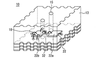
- FIG. 2 is a perspective view showing the internal structure of the semiconductor device 10 of FIG. In FIG. 2, the inside of the semiconductor device is visualized by omitting the metal film 14A, the in-groove metal 14B, and the in-hole metal 14E shown in FIG. 1 and displaying only the outer shape of the insulating sealing material 13. ..
- a plurality of semiconductor elements 22 are mounted on the multilayer board 12. According to one example, the plurality of semiconductor elements 22 include a first semiconductor element 22a and a second semiconductor element 22b. According to another example, three or more semiconductor elements can be mounted on the multilayer board 12.
- the multilayer board 12 is provided with a wiring pattern 32 on the upper surface side.
- the wire 18 connects a plurality of semiconductor elements 22 and a wiring pattern 32 of the multilayer board 12.
- FIG. 3 is a flowchart showing a manufacturing method of the semiconductor device according to the first embodiment. A method of manufacturing a semiconductor device will be described with reference to this flowchart.
- step S1 a plurality of semiconductor elements are mounted on the multilayer board.
- FIG. 4 is a plan view of a multilayer board on which a semiconductor element is mounted.
- the first semiconductor element 22a and the second semiconductor element 22b are mounted on the multilayer substrate 12.
- the first semiconductor element 22a and the second semiconductor element 22b are connected to the wiring pattern 32 or the connection terminal 19 by the wire 18.
- the connection terminal 19 is a pattern in which the input / output power of the semiconductor device is transmitted.
- the separation position 20 is shown by a broken line.
- the separation position 20 is a virtual line that will be a division position when the multilayer board is divided into individual pieces in the future.
- FIG. 4 shows four semiconductor devices before they are divided.
- step S2 the insulating sealing material 13 that covers the plurality of semiconductor elements 22 and the wires 18 is formed on the multilayer substrate 12.
- the insulating sealing material 13 is formed on the entire upper surface of the multilayer substrate 12.
- step S3 a plurality of separation through holes 21 and holes 15 are formed.
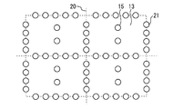
- FIG. 5 is a plan view of the semiconductor device in which the separation through holes 21 and the holes 15 are formed.
- a plurality of separation through holes 21 are formed along the separation position 20.
- the plurality of separation through holes 21 are formed so as to surround the plurality of semiconductor elements in a plan view.
- the plurality of separation through holes 21 penetrate the insulating sealing material 13 and the multilayer substrate 12.
- the hole 15 is formed at a position surrounded by a plurality of separation through holes 21 in a plan view.
- One hole 15 may be formed in a region surrounded by a plurality of separation through holes 21 formed in an annular shape, or a plurality of holes 15 may be formed.
- two holes 15 are formed in a region surrounded by a plurality of separation through holes 21 formed in an annular shape.
- the holes 15 penetrate the insulating sealing material 13 and reach the multilayer substrate 12. In this example, the holes 15 penetrate the insulating encapsulant 13 and the multilayer substrate 12.
- FIG. 6 is a transparent view of the insulating sealing material 13 of FIG. At least a part of the hole 15 is between a plurality of semiconductor elements in a plan view. In this example, there are two holes 15 between the first semiconductor element 22a and the second semiconductor element 22b. According to another example, the hole 15 can be formed at an arbitrary position surrounded by the separation through hole 21 formed in an annular shape.
- a mechanical method, laser processing, or a mold can be used as a method for forming the hole 15 and the separation through hole 21.
- the diameters of the separation through hole 21 and the hole 15 can be matched.
- the diameters of all the separation through holes 21 and all the holes 15 are the same.
- all separation through holes 21 and all holes 15 can be formed with one machining tool, and when laser machining, all separations are performed in a single process.
- the through hole 21 and all the holes 15 can be formed at once.
- step S4 metal is formed in the upper surface of the insulating sealing material 13, in the separation through hole 21, and in the hole 15.
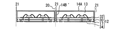
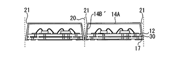
- 7 and 8 are cross-sectional views showing an example of a semiconductor device after metal formation.
- FIG. 7 is a cross-sectional view of the semiconductor device at a position including the separation through hole 21.
- FIG. 7 is a cross-sectional view at a position corresponding to the line AA'of FIG.
- the multilayer board 12 in the example of FIG. 7 includes an insulating layer 34, a wiring pattern 32, a back surface grounding pattern 17, and an interior grounding pattern 30.
- grounding pattern a back surface grounding pattern 17 exposed on the back surface of the multilayer board 12 and an interior grounding pattern 30 provided inside the multilayer board 12 are provided.
- three or more grounding patterns can be provided on different layers of the multilayer board.
- FIG. 7 shows a metal film 14A on the insulating sealing material 13 and a metal portion 14B'provided in the separation through hole 21.
- the metal portion 14B' is in contact with the metal film 14A, the back surface grounding pattern 17, and the interior grounding pattern 30.
- FIG. 8 is a cross-sectional view of the semiconductor device at a position including the hole 15.
- FIG. 8 is a cross-sectional view at a position corresponding to the line BB'of FIG.
- a metal 14E in the hole is formed on the inner wall of the hole 15.
- the holes 15 penetrate the insulating sealing material 13 and the multilayer substrate 12.
- the in-hole metal 14E is in contact with the metal film 14A, the back surface grounding pattern 17, and the interior grounding pattern 30.
- the metal film 14A, the metal portion 14B', and the in-hole metal 14E can be collectively formed by, for example, a vapor deposition or a plating method. Such batch formation contributes to process simplification.
- step S5 the multilayer substrate 12 and the insulating sealing material 13 are split along the plurality of separation through holes 21 to separate the semiconductor device into individual pieces. Due to this individualization, the separation through hole 21 becomes the groove 16 shown in FIG. Along with this, the metal portion 14B'formed on the inner wall of the separation through hole 21 becomes the in-groove metal 14B shown in FIG. By this individualization process, the semiconductor device shown in FIGS. 1 and 2 is completed.
- the groove metal 14B functions as an electromagnetic shield for semiconductor devices.
- the spacing between the in-groove metal 14B contributes to the performance of the electromagnetic shield.
- the spacing between the separation through holes 21 can be set to 1/4 wavelength or less of the high frequency band in which the semiconductor device 10 operates in order to ensure the electromagnetic shielding property of the semiconductor device 10.
- Harmonic power of, for example, 2nd harmonic, 3rd harmonic, and nth harmonic may be generated from the semiconductor element 22. Therefore, the spacing between the groove metal 14B can be determined so that not only the fundamental wave power but also the harmonic power can be shielded. For example, when a molding material having a relative permittivity Er of 5 is used as the insulating sealing material 13 and the operating band of the semiconductor device is 10 GHz, the 1/4 wavelength is 4 mm.
- the distance between two adjacent grooves of the plurality of grooves 16 can be set to 0.6 mm to 1 mm. In this case, as a matter of course, the distance between the metal 14B in the groove is also 0.6 mm to 1 mm.
- the processing accuracy of the separation through hole 21 is approximately 0.3 mm
- the position of a certain groove 16 deviates by a maximum of 0.3 mm from a predetermined position, and the position of the groove 16 adjacent to the groove is also predetermined. It will deviate from the position by a maximum of 0.3 mm. Therefore, as described above, by setting the distance between the plurality of grooves 16 from 0.6 mm to 1 mm, it is possible to reduce the distance between the two grooves while avoiding the connection between the two grooves. By reducing the distance between the groove metal 14B, the shielding property of the harmonic power can be improved.
- the position where the grounding pattern is provided is arbitrary, but for example, the grounding pattern can be formed on the front surface, the back surface, and the inside of the multilayer board 12.
- the metal portion 14B'and the grounding pattern can be easily connected only by forming the metal portion 14B'in the separation through hole 21.
- the metal film 14A, the metal portion 14B', and the in-hole metal 14E are formed before the semiconductor device is separated into individual pieces, so that these are formed after the semiconductor device is separated into individual pieces. Compared with the case, it is suitable for reducing the manufacturing cost by reducing the number of steps and reducing the variation of the electromagnetic shield film.
- the metal 14E in the hole is provided to suppress a malfunction due to resonance in the cavity of the semiconductor device 10.
- the position of the hole 15 By setting the position of the hole 15 to the position between the semiconductor chips 6 in a plan view, interference between the semiconductor elements can be suppressed. In other words, positioning at least a part of the in-hole metal 14E between the first semiconductor element 22a and the second semiconductor element 22b in a plan view suppresses interference between the semiconductor elements.
- the hole 15 can be provided at an arbitrary position.
- the number of holes 15 is not particularly limited. When forming a plurality of holes 15, the two holes 15 should not be in contact with each other in consideration of the processing accuracy of the holes 15.
- the processing variation of the hole 15 is, for example, 0.1 mm. In order to suppress the resonance in the cavity, the radius of the hole 15 can be increased or the number of the holes 15 can be increased.
- FIG. 9 is a cross-sectional view of a semiconductor device showing an example of a metal in a hole according to a modified example.
- the hole 15 shown in FIG. 9 penetrates the insulating sealing material 13 and extends halfway through the multilayer substrate 12 so as not to penetrate the multilayer substrate 12.
- the hole 15 is provided so that the interior grounding pattern 30 is exposed.
- the in-hole metal 14E' is also in contact with the metal film 14A.
- the modification, modification, or alternative described in the first embodiment can be applied to the semiconductor device and the method for manufacturing the semiconductor device according to the following embodiment.
- the differences between the semiconductor device and the method for manufacturing the semiconductor device according to the following embodiments will be mainly described.
- FIG. 10 is a perspective view of the semiconductor device 50 according to the second embodiment.
- the width of the plurality of grooves 52 decreases from the upper surface of the insulating sealing material 13 to the lower surface of the multilayer substrate 12. That is, the groove 52 has a downwardly tapered shape.
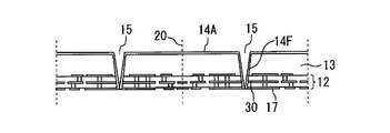
- the holes 15 have a tapered shape that becomes smaller in diameter as they approach the lower surface of the multilayer substrate 12 from the upper surface of the insulating sealing material 13.
- the metal 14F in the hole is formed on the inner wall of the hole 15.
- FIG. 11 is a cross-sectional view of the separation through hole 21.
- the separation through hole 21 is formed in a conical shape along the separation position 20.
- the separation through hole 21 is a hole whose diameter gradually decreases from the upper surface to the lower surface of the semiconductor device. In this example, the separation through hole 21 penetrates the multilayer board 12.
- the metal portion 14B'formed on the inner wall of the separation through hole 21 is connected to the metal film 14A, the back surface grounding pattern 17, and the interior grounding pattern 30.
- FIG. 12 is a cross-sectional view of the hole 15. Similar to the separation through hole 21, the hole 15 is also a hole whose diameter gradually decreases from the upper surface to the lower surface of the semiconductor device.
- the in-hole metal 14F is connected to the metal film 14A, the back surface grounding pattern 17, and the interior grounding pattern 30.
- the plurality of separation through holes 21 and holes 15 have a tapered shape in which the diameter becomes smaller from the upper surface of the insulating sealing material 13 toward the lower surface of the multilayer substrate 12.
- Such tapered separation through holes 21 and holes 15 facilitate thickening of the metal portion 14B'and the in-hole metal 14F at and in the vicinity thereof.
- the metal portion 14B'and the in-hole metal 14F are formed by a thin-film deposition method, the lower end portion thereof and the portion in the vicinity thereof can be easily thickened.
- the thickening of the metal portion 14B'and the in-hole metal 14F ensures that they come into contact with the grounding pattern, so that electromagnetic shielding and cavity resonance can be suppressed regardless of process variation.
- FIG. 13 is a cross-sectional view of the in-hole metal 14F according to the modified example.
- the metal 14F in the hole and the internal grounding pattern 30 can be brought into contact with each other. Since the holes 15 do not penetrate the multilayer board 12, the strength of the semiconductor device can be increased as compared with the case where the holes 15 penetrate the multilayer board 12.
Landscapes
- Engineering & Computer Science (AREA)
- Microelectronics & Electronic Packaging (AREA)
- Structures Or Materials For Encapsulating Or Coating Semiconductor Devices Or Solid State Devices (AREA)
- Non-Metallic Protective Coatings For Printed Circuits (AREA)
- Production Of Multi-Layered Print Wiring Board (AREA)
- Shielding Devices Or Components To Electric Or Magnetic Fields (AREA)
- Internal Circuitry In Semiconductor Integrated Circuit Devices (AREA)
- Manufacturing & Machinery (AREA)
- Physics & Mathematics (AREA)
- Health & Medical Sciences (AREA)
- Electromagnetism (AREA)
- Toxicology (AREA)
Abstract
Description
図1は、実施の形態1に係る半導体装置の斜視図である。半導体装置10は、配線パターンと接地用パターンが形成された多層基板12を備えている。多層基板12の表面、裏面、及び内部には、配線パターン又は接地用パターンが形成されている。多層基板12は、例えばセラミック基板又はガラエポ基板とすることができる。
図10は、実施の形態2に係る半導体装置50の斜視図である。複数の溝52の幅は絶縁性封止材13の上面から多層基板12の下面にかけて減少している。つまり、溝52は、下方向に先細の形状となっている。孔15は絶縁性封止材13の上面から多層基板12の下面に近づくにしたがって小径となるテーパ形状となっている。孔15の内壁に孔内金属14Fが形成されている。
Claims (16)
- 配線パターンと接地用パターンが形成された多層基板と、
前記多層基板の上に実装された複数の半導体素子と、
前記多層基板の上に設けられ、前記複数の半導体素子を覆う絶縁性封止材と、
前記絶縁性封止材の上に設けられた金属膜と、
前記絶縁性封止材の側面上端から前記多層基板の側面下端に至る複数の溝に接して設けられた溝内金属と、
前記絶縁性封止材を貫通し前記多層基板に至る孔の内壁に、前記金属膜と前記接地用パターンとに接して設けられた孔内金属と、を備えた半導体装置。 - 前記接地用パターンは前記多層基板の裏面に露出する裏面接地用パターンを有し、
前記孔は前記絶縁性封止材と前記多層基板を貫通し、
前記孔内金属は前記裏面接地用パターンと接したことを特徴とする請求項1に記載の半導体装置。 - 前記接地用パターンは前記多層基板の内部に設けられた内装接地用パターンを有し、
前記孔は前記絶縁性封止材を貫通しつつ前記多層基板の途中まで及ぶことで前記多層基板を貫通せず、
前記孔内金属は前記内装接地用パターンと接したことを特徴とする請求項1に記載の半導体装置。 - 前記複数の半導体素子と、前記配線パターンを接続するワイヤを備えたことを特徴とする請求項1から3のいずれか1項に記載の半導体装置。
- 前記複数の溝の幅は前記絶縁性封止材の上面から前記多層基板の下面にかけて減少することを特徴とする請求項1から4のいずれか1項に記載の半導体装置。
- 前記孔は前記絶縁性封止材の上面から前記多層基板の下面に近づくにしたがって小径となるテーパ形状となっていることを特徴とする請求項1から5のいずれか1項に記載の半導体装置。
- 前記複数の溝の隣接する2つの溝の間隔は0.6mmから1mmであることを特徴とする請求項1から6のいずれか1項に記載の半導体装置。
- 前記複数の半導体素子は第1半導体素子と第2半導体素子を備え、
前記孔内金属の少なくとも一部は、平面視で前記第1半導体素子と前記第2半導体素子の間にあることを特徴とする請求項1から7のいずれか1項に記載の半導体装置。 - 前記孔と前記孔内金属を複数備えたことを特徴とする請求項1から8のいずれか1項に記載の半導体装置。
- 配線パターンと接地用パターンを有する多層基板の上に複数の半導体素子を実装することと、
前記多層基板の上に前記複数の半導体素子を覆う絶縁性封止材を形成することと、
前記絶縁性封止材と前記多層基板を貫通する複数の分離用貫通孔を、平面視で前記複数の半導体素子を囲むように形成することと、
前記絶縁性封止材を貫通し前記多層基板に至る孔を、平面視で前記複数の分離用貫通孔に囲まれた位置に形成することと、
前記絶縁性封止材の上の金属膜と、前記複数の分離用貫通孔の中に設けられ前記金属膜と前記接地用パターンとに接する金属部と、前記孔の内壁に前記金属膜と前記接地用パターンとに接して設けられた孔内金属と、を形成することと、
前記複数の分離用貫通孔に沿って前記多層基板と前記絶縁性封止材を割り、半導体装置を個片化することと、を備えた半導体装置の製造方法。 - 前記孔の少なくとも一部は、平面視で前記複数の半導体素子の間にあることを特徴とする請求項10に記載の半導体装置の製造方法。
- 前記孔は、前記多層基板を貫通していることを特徴とする請求項10又は11に記載の半導体装置の製造方法。
- 前記孔は、前記多層基板の途中まで及ぶことで前記多層基板を貫通しないことを特徴とする請求項10又は11に記載の半導体装置の製造方法。
- 前記複数の分離用貫通孔と前記孔の径が同じであることを特徴とする請求項10から13のいずれか1項に記載の半導体装置の製造方法。
- 前記金属膜と前記金属部と前記孔内金属は、蒸着又はめっき法で一括して形成することを特徴とする請求項10から14のいずれか1項に記載の半導体装置の製造方法。
- 前記複数の分離用貫通孔と前記孔は、前記絶縁性封止材の上面から前記多層基板の下面に近づくにしたがって小径となるテーパ形状となっていることを特徴とする請求項10から15のいずれか1項に記載の半導体装置の製造方法。
Priority Applications (5)
| Application Number | Priority Date | Filing Date | Title |
|---|---|---|---|
| CN202080096741.8A CN115516619B (zh) | 2020-05-22 | 2020-05-22 | 半导体装置、半导体装置的制造方法 |
| PCT/JP2020/020392 WO2021234969A1 (ja) | 2020-05-22 | 2020-05-22 | 半導体装置、半導体装置の製造方法 |
| US17/758,481 US12463147B2 (en) | 2020-05-22 | 2020-05-22 | Semiconductor device and method for manufacturing semiconductor device |
| JP2022524857A JP7188643B2 (ja) | 2020-05-22 | 2020-05-22 | 半導体装置、半導体装置の製造方法 |
| DE112020007228.2T DE112020007228T5 (de) | 2020-05-22 | 2020-05-22 | Halbleitervorrichtung und Verfahren zum Herstellen einer Halbleitervorrichtung |
Applications Claiming Priority (1)
| Application Number | Priority Date | Filing Date | Title |
|---|---|---|---|
| PCT/JP2020/020392 WO2021234969A1 (ja) | 2020-05-22 | 2020-05-22 | 半導体装置、半導体装置の製造方法 |
Publications (1)
| Publication Number | Publication Date |
|---|---|
| WO2021234969A1 true WO2021234969A1 (ja) | 2021-11-25 |
Family
ID=78708324
Family Applications (1)
| Application Number | Title | Priority Date | Filing Date |
|---|---|---|---|
| PCT/JP2020/020392 Ceased WO2021234969A1 (ja) | 2020-05-22 | 2020-05-22 | 半導体装置、半導体装置の製造方法 |
Country Status (5)
| Country | Link |
|---|---|
| US (1) | US12463147B2 (ja) |
| JP (1) | JP7188643B2 (ja) |
| CN (1) | CN115516619B (ja) |
| DE (1) | DE112020007228T5 (ja) |
| WO (1) | WO2021234969A1 (ja) |
Families Citing this family (3)
| Publication number | Priority date | Publication date | Assignee | Title |
|---|---|---|---|---|
| US12463147B2 (en) * | 2020-05-22 | 2025-11-04 | Mitsubishi Electric Corporation | Semiconductor device and method for manufacturing semiconductor device |
| US11901286B2 (en) * | 2021-01-28 | 2024-02-13 | Taiwan Semiconductor Manufacturing Company, Ltd. | Diagonal via pattern and method |
| CN116013903A (zh) * | 2023-02-23 | 2023-04-25 | 连云港杰瑞电子有限公司 | 具有电磁屏蔽与高导热性能的功率转换模块封装结构及方法 |
Citations (5)
| Publication number | Priority date | Publication date | Assignee | Title |
|---|---|---|---|---|
| US20100109132A1 (en) * | 2008-10-31 | 2010-05-06 | Advanced Semiconductor Engineering, Inc. | Chip package and manufacturing method thereof |
| JP2012039104A (ja) * | 2010-07-15 | 2012-02-23 | Toshiba Corp | 半導体パッケージとそれを用いた携帯通信機器 |
| WO2015194435A1 (ja) * | 2014-06-20 | 2015-12-23 | 株式会社村田製作所 | 回路モジュール及びその製造方法 |
| JP2017191835A (ja) * | 2016-04-12 | 2017-10-19 | Tdk株式会社 | 電子回路モジュール及びその製造方法 |
| JP2019117866A (ja) * | 2017-12-27 | 2019-07-18 | 株式会社村田製作所 | モジュール |
Family Cites Families (6)
| Publication number | Priority date | Publication date | Assignee | Title |
|---|---|---|---|---|
| JP2005340656A (ja) | 2004-05-28 | 2005-12-08 | Matsushita Electric Ind Co Ltd | 高周波集積回路装置及びその製造方法 |
| JP5861260B2 (ja) * | 2011-03-10 | 2016-02-16 | 日本電気株式会社 | 半導体装置の製造方法及び半導体装置 |
| JP6180646B1 (ja) | 2016-02-25 | 2017-08-16 | 三菱電機株式会社 | 半導体パッケージ、及びモジュール |
| JP6683542B2 (ja) * | 2016-06-11 | 2020-04-22 | 新日本無線株式会社 | 電磁シールドを備えた半導体装置の製造方法 |
| JP6800745B2 (ja) | 2016-12-28 | 2020-12-16 | 株式会社ディスコ | 半導体パッケージの製造方法 |
| US12463147B2 (en) * | 2020-05-22 | 2025-11-04 | Mitsubishi Electric Corporation | Semiconductor device and method for manufacturing semiconductor device |
-
2020
- 2020-05-22 US US17/758,481 patent/US12463147B2/en active Active
- 2020-05-22 DE DE112020007228.2T patent/DE112020007228T5/de not_active Withdrawn
- 2020-05-22 CN CN202080096741.8A patent/CN115516619B/zh active Active
- 2020-05-22 WO PCT/JP2020/020392 patent/WO2021234969A1/ja not_active Ceased
- 2020-05-22 JP JP2022524857A patent/JP7188643B2/ja active Active
Patent Citations (5)
| Publication number | Priority date | Publication date | Assignee | Title |
|---|---|---|---|---|
| US20100109132A1 (en) * | 2008-10-31 | 2010-05-06 | Advanced Semiconductor Engineering, Inc. | Chip package and manufacturing method thereof |
| JP2012039104A (ja) * | 2010-07-15 | 2012-02-23 | Toshiba Corp | 半導体パッケージとそれを用いた携帯通信機器 |
| WO2015194435A1 (ja) * | 2014-06-20 | 2015-12-23 | 株式会社村田製作所 | 回路モジュール及びその製造方法 |
| JP2017191835A (ja) * | 2016-04-12 | 2017-10-19 | Tdk株式会社 | 電子回路モジュール及びその製造方法 |
| JP2019117866A (ja) * | 2017-12-27 | 2019-07-18 | 株式会社村田製作所 | モジュール |
Also Published As
| Publication number | Publication date |
|---|---|
| CN115516619A (zh) | 2022-12-23 |
| JP7188643B2 (ja) | 2022-12-13 |
| US12463147B2 (en) | 2025-11-04 |
| DE112020007228T5 (de) | 2023-03-09 |
| JPWO2021234969A1 (ja) | 2021-11-25 |
| CN115516619B (zh) | 2025-02-14 |
| US20230026891A1 (en) | 2023-01-26 |
Similar Documents
| Publication | Publication Date | Title |
|---|---|---|
| CN105304582B (zh) | 封装结构及其制法 | |
| CN107068657B (zh) | 包含天线层的半导体封装件及其制造方法 | |
| TWI569398B (zh) | 半導體元件封裝及其製作方法 | |
| CN101300911B (zh) | 电路模块以及制造电路模块的方法 | |
| JP5837515B2 (ja) | 回路モジュール | |
| EP2787530B1 (en) | High-frequency semiconductor package and high-frequency semiconductor device | |
| US20150296667A1 (en) | Method of manufacturing electronic component | |
| TWI605564B (zh) | 封裝結構及其製法 | |
| JPWO2012023332A1 (ja) | 電子部品及びその製造方法 | |
| WO2021234969A1 (ja) | 半導体装置、半導体装置の製造方法 | |
| JP2019212979A (ja) | 無線モジュールおよびその製造方法並びに電子装置 | |
| JP5904674B2 (ja) | 電子部品実装モジュール及びその製造方法 | |
| TWI491009B (zh) | 晶片級電磁干擾屏蔽結構及製造方法 | |
| TWI532424B (zh) | 蓋板結構及其製作方法 | |
| JP2707996B2 (ja) | 混成集積回路装置およびその製造方法 | |
| CN104103631B (zh) | 电子模块及其制造方法 | |
| US20240063108A1 (en) | Semiconductor package and semiconductor electronic device | |
| JP2004200477A (ja) | 電子回路基板および電子回路装置 | |
| KR20230067288A (ko) | 웨이브 가이드 패키지와 그 제조방법, 및 패키지 하우징 | |
| TWI526152B (zh) | 電子模組及其製造方法 | |
| US12317409B2 (en) | Circuit board local electromagnetic shielding | |
| CN115377666B (zh) | 封装天线的制作方法以及封装天线 | |
| KR102060307B1 (ko) | 반도체 패키지 | |
| JP6441697B2 (ja) | 配線基板および電子装置 | |
| US8294041B2 (en) | Circuit board and manufacturing method thereof |
Legal Events
| Date | Code | Title | Description |
|---|---|---|---|
| 121 | Ep: the epo has been informed by wipo that ep was designated in this application |
Ref document number: 20936429 Country of ref document: EP Kind code of ref document: A1 |
|
| ENP | Entry into the national phase |
Ref document number: 2022524857 Country of ref document: JP Kind code of ref document: A |
|
| 122 | Ep: pct application non-entry in european phase |
Ref document number: 20936429 Country of ref document: EP Kind code of ref document: A1 |
|
| WWG | Wipo information: grant in national office |
Ref document number: 202080096741.8 Country of ref document: CN |
|
| WWG | Wipo information: grant in national office |
Ref document number: 17758481 Country of ref document: US |