WO2020121649A1 - 半導体基板、半導体基板の製造方法及び半導体素子の製造方法 - Google Patents
半導体基板、半導体基板の製造方法及び半導体素子の製造方法 Download PDFInfo
- Publication number
- WO2020121649A1 WO2020121649A1 PCT/JP2019/040926 JP2019040926W WO2020121649A1 WO 2020121649 A1 WO2020121649 A1 WO 2020121649A1 JP 2019040926 W JP2019040926 W JP 2019040926W WO 2020121649 A1 WO2020121649 A1 WO 2020121649A1
- Authority
- WO
- WIPO (PCT)
- Prior art keywords
- layer
- removal layer
- semiconductor
- removal
- etching
- Prior art date
Links
- 239000004065 semiconductor Substances 0.000 title claims abstract description 180
- 239000000758 substrate Substances 0.000 title claims abstract description 150
- 238000000034 method Methods 0.000 title claims description 26
- 238000004519 manufacturing process Methods 0.000 title claims description 23
- 238000005530 etching Methods 0.000 claims abstract description 123
- 239000000463 material Substances 0.000 claims abstract description 44
- 229910001218 Gallium arsenide Inorganic materials 0.000 claims description 14
- 238000005304 joining Methods 0.000 claims description 9
- 238000005520 cutting process Methods 0.000 claims description 3
- 239000010410 layer Substances 0.000 description 270
- 239000010409 thin film Substances 0.000 description 12
- 239000000203 mixture Substances 0.000 description 10
- 239000011368 organic material Substances 0.000 description 8
- VEXZGXHMUGYJMC-UHFFFAOYSA-N Hydrochloric acid Chemical compound Cl VEXZGXHMUGYJMC-UHFFFAOYSA-N 0.000 description 7
- 238000010586 diagram Methods 0.000 description 7
- 239000000243 solution Substances 0.000 description 6
- 238000002474 experimental method Methods 0.000 description 5
- KRHYYFGTRYWZRS-UHFFFAOYSA-N Fluorane Chemical compound F KRHYYFGTRYWZRS-UHFFFAOYSA-N 0.000 description 4
- 239000010408 film Substances 0.000 description 4
- 238000012986 modification Methods 0.000 description 4
- 230000004048 modification Effects 0.000 description 4
- 238000000206 photolithography Methods 0.000 description 4
- 238000001020 plasma etching Methods 0.000 description 4
- 238000001312 dry etching Methods 0.000 description 3
- 230000000694 effects Effects 0.000 description 3
- 239000007789 gas Substances 0.000 description 3
- 239000007788 liquid Substances 0.000 description 3
- 230000003746 surface roughness Effects 0.000 description 3
- 238000001039 wet etching Methods 0.000 description 3
- GRYLNZFGIOXLOG-UHFFFAOYSA-N Nitric acid Chemical compound O[N+]([O-])=O GRYLNZFGIOXLOG-UHFFFAOYSA-N 0.000 description 2
- 238000005229 chemical vapour deposition Methods 0.000 description 2
- 229910010272 inorganic material Inorganic materials 0.000 description 2
- 239000011147 inorganic material Substances 0.000 description 2
- 239000002184 metal Substances 0.000 description 2
- 238000001000 micrograph Methods 0.000 description 2
- 229910017604 nitric acid Inorganic materials 0.000 description 2
- 238000004544 sputter deposition Methods 0.000 description 2
- 238000002230 thermal chemical vapour deposition Methods 0.000 description 2
- KZBUYRJDOAKODT-UHFFFAOYSA-N Chlorine Chemical compound ClCl KZBUYRJDOAKODT-UHFFFAOYSA-N 0.000 description 1
- 230000004913 activation Effects 0.000 description 1
- 229910021417 amorphous silicon Inorganic materials 0.000 description 1
- 239000011248 coating agent Substances 0.000 description 1
- 238000000576 coating method Methods 0.000 description 1
- 238000000151 deposition Methods 0.000 description 1
- 238000007598 dipping method Methods 0.000 description 1
- 238000009826 distribution Methods 0.000 description 1
- 229910000041 hydrogen chloride Inorganic materials 0.000 description 1
- IXCSERBJSXMMFS-UHFFFAOYSA-N hydrogen chloride Substances Cl.Cl IXCSERBJSXMMFS-UHFFFAOYSA-N 0.000 description 1
- 230000010354 integration Effects 0.000 description 1
- 239000011229 interlayer Substances 0.000 description 1
- 239000011259 mixed solution Substances 0.000 description 1
- 150000007524 organic acids Chemical class 0.000 description 1
- 230000002093 peripheral effect Effects 0.000 description 1
- 229910021420 polycrystalline silicon Inorganic materials 0.000 description 1
- 238000012545 processing Methods 0.000 description 1
- 238000004528 spin coating Methods 0.000 description 1
- 239000000126 substance Substances 0.000 description 1
- 238000004381 surface treatment Methods 0.000 description 1
- 238000012546 transfer Methods 0.000 description 1
- 239000011800 void material Substances 0.000 description 1
Images


Classifications
-
- H—ELECTRICITY
- H01—ELECTRIC ELEMENTS
- H01L—SEMICONDUCTOR DEVICES NOT COVERED BY CLASS H10
- H01L21/00—Processes or apparatus adapted for the manufacture or treatment of semiconductor or solid state devices or of parts thereof
- H01L21/02—Manufacture or treatment of semiconductor devices or of parts thereof
- H01L21/04—Manufacture or treatment of semiconductor devices or of parts thereof the devices having potential barriers, e.g. a PN junction, depletion layer or carrier concentration layer
- H01L21/18—Manufacture or treatment of semiconductor devices or of parts thereof the devices having potential barriers, e.g. a PN junction, depletion layer or carrier concentration layer the devices having semiconductor bodies comprising elements of Group IV of the Periodic Table or AIIIBV compounds with or without impurities, e.g. doping materials
- H01L21/30—Treatment of semiconductor bodies using processes or apparatus not provided for in groups H01L21/20 - H01L21/26
- H01L21/302—Treatment of semiconductor bodies using processes or apparatus not provided for in groups H01L21/20 - H01L21/26 to change their surface-physical characteristics or shape, e.g. etching, polishing, cutting
- H01L21/306—Chemical or electrical treatment, e.g. electrolytic etching
- H01L21/30604—Chemical etching
- H01L21/30612—Etching of AIIIBV compounds
-
- H—ELECTRICITY
- H01—ELECTRIC ELEMENTS
- H01L—SEMICONDUCTOR DEVICES NOT COVERED BY CLASS H10
- H01L21/00—Processes or apparatus adapted for the manufacture or treatment of semiconductor or solid state devices or of parts thereof
- H01L21/02—Manufacture or treatment of semiconductor devices or of parts thereof
- H01L21/02002—Preparing wafers
-
- H—ELECTRICITY
- H01—ELECTRIC ELEMENTS
- H01L—SEMICONDUCTOR DEVICES NOT COVERED BY CLASS H10
- H01L21/00—Processes or apparatus adapted for the manufacture or treatment of semiconductor or solid state devices or of parts thereof
- H01L21/02—Manufacture or treatment of semiconductor devices or of parts thereof
- H01L21/04—Manufacture or treatment of semiconductor devices or of parts thereof the devices having potential barriers, e.g. a PN junction, depletion layer or carrier concentration layer
- H01L21/18—Manufacture or treatment of semiconductor devices or of parts thereof the devices having potential barriers, e.g. a PN junction, depletion layer or carrier concentration layer the devices having semiconductor bodies comprising elements of Group IV of the Periodic Table or AIIIBV compounds with or without impurities, e.g. doping materials
- H01L21/30—Treatment of semiconductor bodies using processes or apparatus not provided for in groups H01L21/20 - H01L21/26
- H01L21/302—Treatment of semiconductor bodies using processes or apparatus not provided for in groups H01L21/20 - H01L21/26 to change their surface-physical characteristics or shape, e.g. etching, polishing, cutting
- H01L21/306—Chemical or electrical treatment, e.g. electrolytic etching
- H01L21/30604—Chemical etching
- H01L21/30612—Etching of AIIIBV compounds
- H01L21/30621—Vapour phase etching
-
- H—ELECTRICITY
- H01—ELECTRIC ELEMENTS
- H01L—SEMICONDUCTOR DEVICES NOT COVERED BY CLASS H10
- H01L21/00—Processes or apparatus adapted for the manufacture or treatment of semiconductor or solid state devices or of parts thereof
- H01L21/67—Apparatus specially adapted for handling semiconductor or electric solid state devices during manufacture or treatment thereof; Apparatus specially adapted for handling wafers during manufacture or treatment of semiconductor or electric solid state devices or components ; Apparatus not specifically provided for elsewhere
- H01L21/683—Apparatus specially adapted for handling semiconductor or electric solid state devices during manufacture or treatment thereof; Apparatus specially adapted for handling wafers during manufacture or treatment of semiconductor or electric solid state devices or components ; Apparatus not specifically provided for elsewhere for supporting or gripping
- H01L21/6835—Apparatus specially adapted for handling semiconductor or electric solid state devices during manufacture or treatment thereof; Apparatus specially adapted for handling wafers during manufacture or treatment of semiconductor or electric solid state devices or components ; Apparatus not specifically provided for elsewhere for supporting or gripping using temporarily an auxiliary support
-
- H—ELECTRICITY
- H01—ELECTRIC ELEMENTS
- H01L—SEMICONDUCTOR DEVICES NOT COVERED BY CLASS H10
- H01L21/00—Processes or apparatus adapted for the manufacture or treatment of semiconductor or solid state devices or of parts thereof
- H01L21/70—Manufacture or treatment of devices consisting of a plurality of solid state components formed in or on a common substrate or of parts thereof; Manufacture of integrated circuit devices or of parts thereof
- H01L21/77—Manufacture or treatment of devices consisting of a plurality of solid state components or integrated circuits formed in, or on, a common substrate
- H01L21/78—Manufacture or treatment of devices consisting of a plurality of solid state components or integrated circuits formed in, or on, a common substrate with subsequent division of the substrate into plural individual devices
- H01L21/7806—Manufacture or treatment of devices consisting of a plurality of solid state components or integrated circuits formed in, or on, a common substrate with subsequent division of the substrate into plural individual devices involving the separation of the active layers from a substrate
-
- H—ELECTRICITY
- H01—ELECTRIC ELEMENTS
- H01L—SEMICONDUCTOR DEVICES NOT COVERED BY CLASS H10
- H01L21/00—Processes or apparatus adapted for the manufacture or treatment of semiconductor or solid state devices or of parts thereof
- H01L21/02—Manufacture or treatment of semiconductor devices or of parts thereof
- H01L21/02104—Forming layers
- H01L21/02365—Forming inorganic semiconducting materials on a substrate
- H01L21/02367—Substrates
- H01L21/0237—Materials
- H01L21/02387—Group 13/15 materials
- H01L21/02392—Phosphides
-
- H—ELECTRICITY
- H01—ELECTRIC ELEMENTS
- H01L—SEMICONDUCTOR DEVICES NOT COVERED BY CLASS H10
- H01L21/00—Processes or apparatus adapted for the manufacture or treatment of semiconductor or solid state devices or of parts thereof
- H01L21/02—Manufacture or treatment of semiconductor devices or of parts thereof
- H01L21/02104—Forming layers
- H01L21/02365—Forming inorganic semiconducting materials on a substrate
- H01L21/02367—Substrates
- H01L21/0237—Materials
- H01L21/02387—Group 13/15 materials
- H01L21/02395—Arsenides
-
- H—ELECTRICITY
- H01—ELECTRIC ELEMENTS
- H01L—SEMICONDUCTOR DEVICES NOT COVERED BY CLASS H10
- H01L21/00—Processes or apparatus adapted for the manufacture or treatment of semiconductor or solid state devices or of parts thereof
- H01L21/02—Manufacture or treatment of semiconductor devices or of parts thereof
- H01L21/02104—Forming layers
- H01L21/02365—Forming inorganic semiconducting materials on a substrate
- H01L21/02436—Intermediate layers between substrates and deposited layers
- H01L21/02439—Materials
- H01L21/02455—Group 13/15 materials
- H01L21/02463—Arsenides
-
- H—ELECTRICITY
- H01—ELECTRIC ELEMENTS
- H01L—SEMICONDUCTOR DEVICES NOT COVERED BY CLASS H10
- H01L21/00—Processes or apparatus adapted for the manufacture or treatment of semiconductor or solid state devices or of parts thereof
- H01L21/02—Manufacture or treatment of semiconductor devices or of parts thereof
- H01L21/02104—Forming layers
- H01L21/02365—Forming inorganic semiconducting materials on a substrate
- H01L21/02436—Intermediate layers between substrates and deposited layers
- H01L21/02494—Structure
- H01L21/02496—Layer structure
- H01L21/02502—Layer structure consisting of two layers
-
- H—ELECTRICITY
- H01—ELECTRIC ELEMENTS
- H01L—SEMICONDUCTOR DEVICES NOT COVERED BY CLASS H10
- H01L21/00—Processes or apparatus adapted for the manufacture or treatment of semiconductor or solid state devices or of parts thereof
- H01L21/02—Manufacture or treatment of semiconductor devices or of parts thereof
- H01L21/02104—Forming layers
- H01L21/02365—Forming inorganic semiconducting materials on a substrate
- H01L21/02518—Deposited layers
- H01L21/02521—Materials
- H01L21/02538—Group 13/15 materials
- H01L21/02543—Phosphides
-
- H—ELECTRICITY
- H01—ELECTRIC ELEMENTS
- H01L—SEMICONDUCTOR DEVICES NOT COVERED BY CLASS H10
- H01L21/00—Processes or apparatus adapted for the manufacture or treatment of semiconductor or solid state devices or of parts thereof
- H01L21/02—Manufacture or treatment of semiconductor devices or of parts thereof
- H01L21/02104—Forming layers
- H01L21/02365—Forming inorganic semiconducting materials on a substrate
- H01L21/02518—Deposited layers
- H01L21/02521—Materials
- H01L21/02538—Group 13/15 materials
- H01L21/02546—Arsenides
-
- H—ELECTRICITY
- H01—ELECTRIC ELEMENTS
- H01L—SEMICONDUCTOR DEVICES NOT COVERED BY CLASS H10
- H01L2221/00—Processes or apparatus adapted for the manufacture or treatment of semiconductor or solid state devices or of parts thereof covered by H01L21/00
- H01L2221/67—Apparatus for handling semiconductor or electric solid state devices during manufacture or treatment thereof; Apparatus for handling wafers during manufacture or treatment of semiconductor or electric solid state devices or components; Apparatus not specifically provided for elsewhere
- H01L2221/683—Apparatus for handling semiconductor or electric solid state devices during manufacture or treatment thereof; Apparatus for handling wafers during manufacture or treatment of semiconductor or electric solid state devices or components; Apparatus not specifically provided for elsewhere for supporting or gripping
- H01L2221/68304—Apparatus for handling semiconductor or electric solid state devices during manufacture or treatment thereof; Apparatus for handling wafers during manufacture or treatment of semiconductor or electric solid state devices or components; Apparatus not specifically provided for elsewhere for supporting or gripping using temporarily an auxiliary support
- H01L2221/68363—Apparatus for handling semiconductor or electric solid state devices during manufacture or treatment thereof; Apparatus for handling wafers during manufacture or treatment of semiconductor or electric solid state devices or components; Apparatus not specifically provided for elsewhere for supporting or gripping using temporarily an auxiliary support used in a transfer process involving transfer directly from an origin substrate to a target substrate without use of an intermediate handle substrate
-
- H—ELECTRICITY
- H01—ELECTRIC ELEMENTS
- H01L—SEMICONDUCTOR DEVICES NOT COVERED BY CLASS H10
- H01L2221/00—Processes or apparatus adapted for the manufacture or treatment of semiconductor or solid state devices or of parts thereof covered by H01L21/00
- H01L2221/67—Apparatus for handling semiconductor or electric solid state devices during manufacture or treatment thereof; Apparatus for handling wafers during manufacture or treatment of semiconductor or electric solid state devices or components; Apparatus not specifically provided for elsewhere
- H01L2221/683—Apparatus for handling semiconductor or electric solid state devices during manufacture or treatment thereof; Apparatus for handling wafers during manufacture or treatment of semiconductor or electric solid state devices or components; Apparatus not specifically provided for elsewhere for supporting or gripping
- H01L2221/68304—Apparatus for handling semiconductor or electric solid state devices during manufacture or treatment thereof; Apparatus for handling wafers during manufacture or treatment of semiconductor or electric solid state devices or components; Apparatus not specifically provided for elsewhere for supporting or gripping using temporarily an auxiliary support
- H01L2221/68368—Apparatus for handling semiconductor or electric solid state devices during manufacture or treatment thereof; Apparatus for handling wafers during manufacture or treatment of semiconductor or electric solid state devices or components; Apparatus not specifically provided for elsewhere for supporting or gripping using temporarily an auxiliary support used in a transfer process involving at least two transfer steps, i.e. including an intermediate handle substrate
Definitions
- the present invention relates to a semiconductor substrate, a method for manufacturing a semiconductor substrate, and a method for manufacturing a semiconductor element using the semiconductor substrate.
- the removal layer and the semiconductor epitaxial layer are formed on the GaAs substrate as the base substrate for growing the semiconductor epitaxial layer
- the removal layer is removed with an etching solution such as hydrofluoric acid.
- the semiconductor epitaxial layer is separated from the GaAs substrate by.
- the etching rate of the GaAs substrate and the semiconductor epitaxial layer is significantly lower than the etching rate of the removal layer.
- the removal layer When the removal layer is removed by etching, the surface of the GaAs substrate in contact with the removal layer and the bottom surface of the semiconductor epitaxial layer are extremely flat. As a result, there is a problem that the surface of the GaAs substrate may be joined to the bottom surface of the separated semiconductor epitaxial layer after the removal layer is removed by etching. If the surface of the GaAs substrate and the bottom surface of the semiconductor epitaxial layer are joined after the removal layer is removed by etching, the semiconductor epitaxial layer cannot be separated from the GaAs substrate. There is a demand for a technique for preventing the separated bottom surface of the semiconductor epitaxial layer from joining.
- the present invention has been made in view of these points, and an object thereof is to prevent the surface of the base substrate and the bottom surface of the separated semiconductor epitaxial layer from joining even after the removal layer is removed.
- a semiconductor substrate according to a first aspect of the present invention is a base substrate, a first removal layer provided on the base substrate, a second removal layer provided above the first removal layer, and a second removal layer provided above the first removal layer.
- a semiconductor epitaxial layer provided above the removal layer, and an etching rate of the second removal layer with respect to the predetermined etching material is higher than an etching rate of the first removal layer with respect to the predetermined etching material.
- the thickness of the first removal layer may be greater than the thickness of the second removal layer.
- the surface of the first removal layer exposed when the second removal layer is removed by etching using the predetermined etching material is rougher than the surface of the semiconductor epitaxial layer on the second removal layer side. May be.
- the base substrate is made of GaAs
- the semiconductor epitaxial layer is made of Al t Ga 1-t As (0 ⁇ t ⁇ 1)
- the first removal layer is made of Al x Ga 1-x As( 0.6 ⁇ x ⁇ 0.8)
- the second removal layer may be formed of Al y Ga 1-y As (0.7 ⁇ y ⁇ 1, y>x).
- the semiconductor epitaxial layer may be made of Al t Ga 1-t As (0 ⁇ t ⁇ 0.6).
- the base substrate may be made of InP, and the semiconductor epitaxial layer may be In 1-x Ga x As y P 1-y (0 ⁇ x, y ⁇ 1).
- the third removal layer may further include a third removal layer provided between the first removal layer and the second removal layer, and an etching rate of the third removal layer with respect to the predetermined etching material may be the same with respect to the predetermined etching material. It may be higher than the etching rate of the first removal layer and lower than the etching rate of the second removal layer with respect to the predetermined etching material.
- a support member for supporting the semiconductor epitaxial layer may be further provided so that the semiconductor epitaxial layer is located above the base substrate.
- the support member may be in contact with the base substrate, the first removal layer, the second removal layer, and the semiconductor epitaxial layer.
- the support member may have a shape in which a part of a region in contact with the second removal layer has a thickness smaller than that of other regions.
- a method of manufacturing a semiconductor substrate according to a second aspect of the present invention includes a step of preparing a base substrate, a step of forming a first removal layer on the base substrate, and a predetermined etching process above the first removal layer. Forming a second removal layer having an etching rate with respect to a material higher than an etching rate of the first removal layer with respect to the predetermined etching material; and forming a semiconductor epitaxial layer above the second removal layer, Forming the semiconductor epitaxial layer, and providing a support member for supporting the semiconductor epitaxial layer so that the semiconductor epitaxial layer is located above the base substrate.
- a method of manufacturing a semiconductor device includes a step of preparing the semiconductor substrate, a removal step of removing the second removal layer by etching using the predetermined etching material, And a bonding step of bonding the semiconductor epitaxial layer to a destination substrate different from the base substrate after the removing step.
- the semiconductor substrate further has a supporting member for supporting the semiconductor epitaxial layer so that the semiconductor epitaxial layer is located above the base substrate, and the manufacturing method includes the removing step and the joining step. In between, a step of cutting the supporting member may be further included.
- the present invention it is possible to prevent the surface of the base substrate and the bottom surface of the separated semiconductor epitaxial layer from being bonded even after the removal layer is removed.
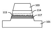
- FIG. 1 is a schematic diagram showing the configuration of the semiconductor substrate 1 of this embodiment.
- FIG. 1 shows a sectional structure of a semiconductor epitaxial wafer.
- the semiconductor substrate 1 includes a base substrate 101, a removal layer 102 provided on the base substrate 101, and a semiconductor epitaxial layer 103 provided above the removal layer 102.
- the base substrate 101 is a base material substrate for crystal-growing a semiconductor epitaxial layer.
- the base substrate 101 is made of a III-V group semiconductor will be described as an example, but the base substrate 101 may be made of a material other than a III-V group semiconductor.
- the removal layer 102 is a layer that is planned to be removed at least partially by etching.
- the removal layer 102 includes a first removal layer 104 provided on the base substrate 101 and a second removal layer 105 provided on the first removal layer 104.
- the etching rate of the second removal layer 105 with respect to the predetermined etching material is higher than the etching rate of the first removal layer 104 with respect to the predetermined etching material.
- the predetermined etching material is an etching solution or an etching gas in which the etching rate of the second removal layer 105 is sufficiently higher than the etching rate of the semiconductor epitaxial layer 103.
- the etching rate of the second removal layer 105 is, for example, twice or more the etching rate of the first removal layer 104.
- the specified etching material is referred to as the used etching material.
- the etching material used include hydrochloric acid, hydrofluoric acid, nitric acid, a mixed solution of hydrochloric acid and nitric acid, organic acid, hydrogen chloride gas, and chlorine gas.
- the etching rate of the second removal layer 105 with respect to the above-described predetermined etching material is higher than the etching rate of the first removal layer 104 with respect to the used etching material, when all of the second removal layer 105 is removed by etching, At least a part of the first removal layer 104 remains. At this time, since the first removal layer 104 is in a state where etching is in progress, the surface of the first removal layer 104 exposed when the second removal layer 105 is removed by etching using the etching material used is , Rougher than the surface of the semiconductor epitaxial layer 103 on the second removal layer 105 side. Therefore, even if the semiconductor epitaxial layer 103 separated by the removal of the first removal layer 104 contacts the first removal layer 104, the state where the semiconductor epitaxial layer 103 and the first removal layer 104 are not bonded is maintained. It
- the base substrate 101 is, for example, a GaAs substrate.
- the semiconductor epitaxial layer 103 is a semiconductor epitaxial layer to be removed from the base substrate 101, and is composed of, for example, Al t Ga 1-t As (0 ⁇ t ⁇ 1).
- the first removal layer 104 is composed of, for example, Al x Ga 1-x As (0.6 ⁇ x ⁇ 0.8), and the second removal layer 105 is composed of, for example, Al y Ga 1-y As(0. 7 ⁇ y ⁇ 1, y>x).
- the first removal layer 104 is Al x Ga 1-x As (0.75 ⁇ x ⁇ 0.8)
- the second removal layer 105 is Is more preferably Al y Ga 1-y As (0.8 ⁇ y ⁇ 1).
- the material composition of the semiconductor layer forming the bottom surface (the surface on the second removal layer 105 side) of the semiconductor epitaxial layer 103 in contact with the second removal layer 105 is Al t Ga 1-t As (0 ⁇ t ⁇ 0.6 ) Is preferred. It is more preferable that the semiconductor layer forming the bottom surface of the semiconductor epitaxial layer 103 in contact with the second removal layer 105 is a GaAs layer.
- the first removal layer 104 has a thickness larger than that of the second removal layer 105. May have a large thickness.
- the thickness of the first removal layer 104 and the thickness of the second removal layer 105 are the same when the second removal layer 105 is removed, even when the degree of progress of etching varies depending on the location of the first removal layer 104.
- the thickness may be such that at least a part of the first removal layer 104 remains over the entire area of the first removal layer 104.
- the semiconductor substrate 1 was prototyped and etched.
- the base substrate 101 was a GaAs substrate.
- the composition of the first removal layer 104 was Al x Ga 1-x As (0.75 ⁇ x ⁇ 0.8).
- the composition of the second removal layer 105 was Al y Ga 1-y As (0.8 ⁇ y ⁇ 1).
- the composition of the semiconductor epitaxial layer 103 was Al t Ga 1-t As (0 ⁇ t ⁇ 0.6).
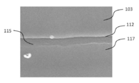
- FIG. 2A is a semiconductor substrate micrograph used in the experiment.
- FIG. 2B is a schematic diagram showing experimental results. As shown in FIG. 2B, the microscope photograph shown in FIG. 2A is a photograph obtained by inclining the semiconductor substrate 1 and taking an image with an electron microscope (Scanning Electron Microscope: SEM) from the direction of the arrow.
- SEM Scanning Electron Microscope
- the photograph shown in FIG. 2A shows a state in which the second removal layer 105 is completely removed by etching with the etching liquid, and a part of the first removal layer 104 is etched.
- FIG. 2A it can also be confirmed that the lower surface 112 of the semiconductor epitaxial layer 103 is flat, whereas the upper surface 115 of the residual layer 117 is a rough surface with unevenness. This is because the etching rate of the first removal layer 104 with respect to the used etching solution is lower than the etching rate of the second removal layer 105, and while the second removal layer 105 is completely etched away, the first removal layer 104 is removed. Due to the etching of only a part of.
- the second removal layer 105 After removing the second removal layer 105 by etching, the second removal layer 105 is removed by etching because the upper surface of the residual layer 117, which is a layer in which a part of the first removal layer 104 remains, is rough. After that, the semiconductor epitaxial layer 103 is difficult to bond to the surface on the side of the base substrate 101 (that is, the residual layer 117 remaining on the base substrate 101). Therefore, the semiconductor epitaxial layer 103 can be well separated from the base substrate 101.
- At least the surface roughness Ra of the bottom surface of the semiconductor epitaxial layer 103 (that is, the surface on the side of the removed second removal layer 105) is preferably smaller than the surface roughness Rb of the upper surface of the residual layer 117.
- the surface roughness is, for example, an average roughness measured by an atomic force microscope (AFM).
- the semiconductor epitaxial layer 103 is not exposed It has been confirmed that the semiconductor epitaxial layer 103 can be removed from the base substrate 101 without being bonded to the first removal layer 104.
- the composition of the first removal layer 104 is Al x Ga 1-x As (0.6 ⁇ x ⁇ 0.8), and the composition of the second removal layer 105 is Al y Ga 1-y As(0 .7 ⁇ y ⁇ 1, y>x), there is a large difference between the etching rate of the first removal layer 104 and the etching rate of the second removal layer 105. It will be appreciated that a combination of layers 105 can be selected.
- the semiconductor substrate 1 includes the first removal layer 104 and the second removal layer 105.
- other removal layers may be included. At this time, it is desirable to stack the removal layers 102 in order of increasing etching rate from the side in contact with the base substrate 101 to the side in contact with the semiconductor epitaxial layer 103.
- the semiconductor substrate 1 may further include a third removal layer between the first removal layer 104 and the second removal layer 105.
- the etching rate of the third removal layer with respect to the used etching material is higher than the etching rate of the first removal layer 104 with respect to the used etching material and lower than the etching rate of the second removal layer 105 with respect to the used etching material.
- the base substrate 101 is a GaAs substrate
- the present invention can be applied to a case where the base substrate 101 is another III-V group semiconductor epitaxial substrate.
- the semiconductor substrate 1 for example, the base substrate 101 is an InP substrate and the semiconductor epitaxial layer 103 is a lattice-matched or substantially lattice-matched semiconductor epitaxial layer on the InP substrate (for example, In 1-x Ga x As y P 1-y ( 0 ⁇ x, y ⁇ 1)).
- the removal layer 102 is a semiconductor layer that is lattice-matched or substantially lattice-matched on the InP substrate.
- the first removal layer 104 is In 0.52 Al 0.48 As
- the second removal layer 105 is In 0.53 Ga 0.47 As.
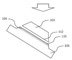
- FIG. 4 is a diagram for explaining a method for manufacturing a semiconductor element.
- the semiconductor substrate 1 shown in FIG. 1 is prepared.
- the semiconductor substrate 1 is manufactured by forming the laminated structure including the first removal layer 104 and the second removal layer 105 on the base substrate 101 and then forming the semiconductor epitaxial layer 103 on the second removal layer 105. ..
- the semiconductor epitaxial layer 103 has a semiconductor laminated structure for forming a predetermined element.
- the predetermined element is an arbitrary element made of a semiconductor, such as a light emitting diode, a transistor, a sensor, or the like.
- a semiconductor element may be manufactured using the manufactured semiconductor substrate 1 instead of manufacturing the semiconductor substrate 1. That is, the step of preparing the semiconductor substrate 1 in which the first removal layer 104, the second removal layer 105, and the semiconductor epitaxial layer 103 are already formed on the base substrate 101 may be the first step of the method for manufacturing a semiconductor device. .. Further, the step of preparing the semiconductor substrate 1 in which the predetermined element structure or a part of the predetermined element structure is already formed in the semiconductor epitaxial layer 103 may be the first step of the method for manufacturing a semiconductor element.
- an island is formed in which at least part (for example, the outer peripheral surface) of the second removal layer 105 to be removed by etching is exposed.
- the island shown in FIG. 4A is formed by etching a predetermined range from the outer periphery of the semiconductor epitaxial layer 103, the first removal layer 104, and the second removal layer 105 in the semiconductor substrate 1.
- the first removal layer 104 and the second removal layer 105 are etched with a predetermined etching solution.
- the etching is continued until the second removal layer 105 is completely removed, and the etching is stopped when the second removal layer 105 is removed.
- the void 114 is formed by completely removing the second removal layer 105.
- Part of the region of the first removal layer 104 on the second removal layer 105 side is removed, and irregularities are formed on the surface of the first removal layer 104 opposite to the side in contact with the base substrate 101.
- the residual layer 117 of the first removal layer 104 having the roughened surface is formed.
- the formed unevenness is exaggeratedly drawn.
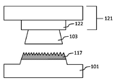
- the semiconductor epitaxial layer 103 is separated from the base substrate 101 by using, for example, a pickup substrate 121 having a pickup bump 122.
- the pickup bump 122 is, for example, an organic material layer, and can be formed by applying a photosensitive organic material on a semiconductor substrate and performing a standard photolithography process.
- the organic material layer may be formed, for example, by coating an organic material on a pickup base substrate which is a base of the pickup substrate 121 by a spin coating method, a dipping method, or the like, or by forming an organic material film on the pickup base substrate. You may form by pasting on.
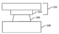
- the semiconductor epitaxial layer 103 separated from the base substrate 101 by the pickup substrate 121 is pressed onto and bonded to the destination substrate 130.
- a surface treatment process such as activation treatment of the joining surface may be performed.
- another semiconductor layer, a metal layer, or an insulating film layer may be provided on the movement-destination substrate 130 as a material layer different from the material of the movement-destination substrate 130.
- the pickup substrate 121 is separated (not shown).
- Manufacture of the semiconductor element is completed by appropriately forming an interlayer insulating film, a metal wiring film, or the like on the semiconductor epitaxial layer 103 after separating the pickup substrate 121.
- the semiconductor epitaxial layer 103 is positioned above the base substrate 101.
- a supporting member for supporting the semiconductor epitaxial layer 103 may be provided.
- FIG. 5 is a diagram showing an example in which the support member 106 is provided.
- the support member 106 is, for example, a semiconductor thin film, an organic material thin film, or an inorganic material thin film that connects the semiconductor epitaxial layer 103 and the base substrate 101.
- the support member 106 is formed so that, for example, a part of the region is in contact with the side surfaces of the first removal layer 104 and the second removal layer 105. Part of the support member 106 may be formed so as to extend to the upper surface of the semiconductor epitaxial layer 103 or the surface where the base substrate 101 is exposed.
- the thin film forming the support member 106 has a sufficiently lower etching rate with respect to the etching material used for removing the second removal layer 105 than the etching rate of the second removal layer 105, so that the second removal layer 105 is removed. At that time, the semiconductor epitaxial layer 103 and the base substrate 101 remain in a bonded state.
- the support member 106 may be formed as follows, for example.
- the supporting member 106 is formed of a semiconductor thin film such as amorphous Si or poly Si, for example, a sputtering method, a thermal CVD (Chemical Vapor Deposition) method, a PCVD (Plasma Chemical Vapor Deposition) method, or an LPCVD (Low pressure Chemical Vapor) method is used.
- the semiconductor thin film can be formed by appropriately selecting the Deposition method or the like.
- the structure of the support member 106 can be formed by dry etching such as photolithography and RIE (Reactive Ion Etching) method or wet etching using a predetermined etching solution.
- the inorganic thin film can be formed by, for example, a sputtering method, a thermal CVD method, a PCVD method, or the like.
- the structure of the support member 106 can be formed by dry etching such as photolithography and RIE, or wet etching using a predetermined etching solution.
- the etching liquid used for forming the structure of the support member 106 is an etching liquid having a smaller etching rate for the first removal layer, the second removal layer, and the semiconductor epitaxial layer 103 than the etching rate for the support member 106. It is desirable to select the etching gas.
- the support member 106 in the step of removing the second removal layer 105, the probability that the semiconductor epitaxial layer 103 contacts the first removal layer 104 or the base substrate 101 can be reduced.
- the thin film forming the support member 106 is damaged or does not remain due to the provision of the first removal layer 104 having an etching rate lower than that of the second removal layer 105, It is possible to prevent the semiconductor epitaxial layer 103 from joining with the base substrate 101.
- the supporting member 106 is preferably formed so as to be easily cut by applying a force in a direction in which the semiconductor epitaxial layer 103 is separated from the base substrate 101.
- the support member 106 has a shape in which a part of the region in contact with the side surface of the second removal layer 105 has a thickness smaller than the thickness of the other region (for example, a groove shape), the second removal layer 105 is removed. After being supported, the supporting member 106 is easily cut.
- the method may further include the step of cutting the support member 106 by pulling up the semiconductor epitaxial layer 103.
- the supporting member 106 in which the thickness of the predetermined region is smaller than the thickness of the other regions can be manufactured by the following method, for example. First, a region other than a region where the thickness is reduced (for example, a region where a groove is formed) is covered with a resist. Subsequently, the resist is removed after wet etching using an etchant for etching the material of the supporting member 106 or dry etching such as RIE so that the material has a predetermined thickness.
- the etching rate of the second removal layer 105 with respect to the predetermined etching material is higher than the etching rate of the first removal layer 104 is illustrated, but the etching rate of the first removal layer 104 is The etching rate of the second removal layer 105 may be higher than the etching rate.
- the thickness of the first removal layer 104 is set so that at least a part of the first removal layer 104 remains when the removal of the second removal layer 105 by etching is completed. It is required to be larger than the thickness.
- the semiconductor substrate 1 of the present invention has at least two removal layers having different etching rates between the semiconductor epitaxial layer 103, which is to be separated from the base substrate 101, and the base substrate 101. Therefore, it is possible to prevent the semiconductor epitaxial layer 103 from being bonded to the base substrate 101 after the semiconductor epitaxial layer 103 is separated.
- the semiconductor epitaxial layer 103 having a flat surface is easily moved to the destination substrate 130, and the semiconductor epitaxial layer 103 after the movement is processed to perform various kinds of processing.
- a semiconductor device can be manufactured.
- the present invention has been described above using the embodiments, the technical scope of the present invention is not limited to the scope described in the above embodiments, and various modifications and changes are possible within the scope of the gist thereof. is there.
- the specific embodiment of the distribution/integration of the device is not limited to the above-described embodiment, and all or a part thereof may be functionally or physically distributed/integrated in arbitrary units to be configured.
- You can Further, a new embodiment that occurs due to an arbitrary combination of a plurality of embodiments is also included in the embodiment of the present invention. The effect of the new embodiment produced by the combination has the effect of the original embodiment.
Landscapes
- Engineering & Computer Science (AREA)
- Physics & Mathematics (AREA)
- Condensed Matter Physics & Semiconductors (AREA)
- General Physics & Mathematics (AREA)
- Manufacturing & Machinery (AREA)
- Computer Hardware Design (AREA)
- Microelectronics & Electronic Packaging (AREA)
- Power Engineering (AREA)
- Chemical & Material Sciences (AREA)
- Chemical Kinetics & Catalysis (AREA)
- General Chemical & Material Sciences (AREA)
- Recrystallisation Techniques (AREA)
- Weting (AREA)
- Drying Of Semiconductors (AREA)
- Cleaning Or Drying Semiconductors (AREA)
- Led Devices (AREA)
- Bipolar Transistors (AREA)
- Physical Deposition Of Substances That Are Components Of Semiconductor Devices (AREA)
- Mechanical Treatment Of Semiconductor (AREA)
Abstract
除去層を除去した後にもベース基板の表面と分離した半導体エピタキシャル層の底面とが接合しないようにするために、半導体基板1は、ベース基板101と、ベース基板101上に設けられた第1除去層104と、第1除去層104の上方に設けられた第2除去層105と、第2除去層105の上方に設けられた半導体エピタキシャル層103と、を有し、所定のエッチング材料に対する第2除去層105のエッチング速度が、所定のエッチング材料に対する第1除去層104のエッチング速度よりも大きい。
Description
本発明は、半導体基板、半導体基板の製造方法及び当該半導体基板を用いた半導体素子の製造方法に関する。
従来、半導体基板上に除去層及び半導体エピタキシャル層を形成し、エッチングにより除去層を除去することで半導体エピタキシャル層を半導体基板から分離する技術が知られている(例えば、特許文献1を参照)。
特許文献1に記載された技術では、半導体エピタキシャル層を成長させるためのベース基板としてのGaAs基板上に除去層及び半導体エピタキシャル層を形成した後に、弗酸などのエッチング液によって除去層を除去することにより半導体エピタキシャル層をGaAs基板から分離する。この方法で半導体エピタキシャル層をGaAs基板から分離する場合、GaAs基板及び半導体エピタキシャル層のエッチング速度が除去層のエッチング速度よりも格段に小さいことが想定されている。
エッチングにより除去層を除去した場合、除去層と接するGaAs基板の表面及び半導体エピタキシャル層の底面は非常に平坦な面となる。その結果、除去層をエッチングにより除去した後に、GaAs基板の表面と分離した半導体エピタキシャル層の底面とが接合してしまう場合があるという問題が生じていた。除去層をエッチングにより除去した後にGaAs基板の表面と半導体エピタキシャル層の底面とが接合すると、半導体エピタキシャル層をGaAs基板から分離することができなくなるため、除去層を除去した後にもGaAs基板の表面と分離した半導体エピタキシャル層の底面とが接合しないようにする技術が求められている。
そこで、本発明はこれらの点に鑑みてなされたものであり、除去層を除去した後にもベース基板の表面と分離した半導体エピタキシャル層の底面とが接合しないようにすることを目的とする。
本発明の第1の態様の半導体基板は、ベース基板と、前記ベース基板上に設けられた第1除去層と、前記第1除去層の上方に設けられた第2除去層と、前記第2除去層の上方に設けられた半導体エピタキシャル層と、を有し、所定のエッチング材料に対する前記第2除去層のエッチング速度が、前記所定のエッチング材料に対する前記第1除去層のエッチング速度よりも大きい。前記第2除去層の厚みよりも前記第1除去層の厚みが大きくてもよい。
前記所定のエッチング材料を用いたエッチングにより前記第2除去層が除去された時点で露出している前記第1除去層の表面が、前記半導体エピタキシャル層の前記第2除去層側の面よりも粗くてもよい。
前記ベース基板がGaAsにより構成されており、前記半導体エピタキシャル層がAltGa1-tAs(0≦t≦1)により構成されており、前記第1除去層がAlxGa1-xAs(0.6<x≦0.8)により構成されており、前記第2除去層がAlyGa1-yAs(0.7<y≦1、y>x)により構成されていてもよい。前記半導体エピタキシャル層がAltGa1-tAs(0≦t≦0.6)により構成されていてもよい。
前記ベース基板がInPにより構成されており、前記半導体エピタキシャル層がIn1-xGaxAsyP1-y(0≦x、y≦1)であってもよい。
前記第1除去層と前記第2除去層との間に設けられた第3除去層をさらに有し、前記所定のエッチング材料に対する前記第3除去層のエッチング速度は、前記所定のエッチング材料に対する前記第1除去層のエッチング速度よりも大きく、前記所定のエッチング材料に対する前記第2除去層のエッチング速度よりも小さくてもよい。
前記半導体エピタキシャル層が前記ベース基板の上方に位置するように前記半導体エピタキシャル層を支持するための支持部材をさらに有してもよい。前記支持部材は、前記ベース基板、前記第1除去層、前記第2除去層及び前記半導体エピタキシャル層に接してもよい。前記支持部材は、前記第2除去層に接する領域の一部の厚みが他の領域の厚みよりも小さい形状を有してもよい。
本発明の第2の態様の半導体基板の製造方法は、ベース基板を準備する工程と、前記ベース基板上に第1除去層を形成する工程と、前記第1除去層の上方に、所定のエッチング材料に対するエッチング速度が、前記所定のエッチング材料に対する前記第1除去層のエッチング速度よりも大きい第2除去層を形成する工程と、前記第2除去層の上方に半導体エピタキシャル層を形成する工程と、前記半導体エピタキシャル層を形成した後に、前記半導体エピタキシャル層が前記ベース基板の上方に位置するように前記半導体エピタキシャル層を支持するための支持部材を設ける工程と、を有する。
本発明の第3の態様の半導体素子の製造方法は、上記の半導体基板を準備する工程と、前記所定のエッチング材料を用いてエッチングすることにより前記第2除去層を除去する除去工程と、前記除去工程の後に、前記半導体エピタキシャル層を前記ベース基板と異なる移動先基板に接合する接合工程と、を有する。前記半導体基板が、前記半導体エピタキシャル層が前記ベース基板の上方に位置するように前記半導体エピタキシャル層を支持するための支持部材をさらに有し、前記製造方法は、前記除去工程と前記接合工程との間に、前記支持部材を切断する工程をさらに有してもよい。
本発明によれば、除去層を除去した後にもベース基板の表面と分離した半導体エピタキシャル層の底面とが接合しないようにすることができるという効果を奏する。
[半導体基板1の構成]
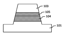
図1は、本実施形態の半導体基板1の構成を示す模式図である。図1は、半導体エピタキシャルウエハの断面構造を示している。半導体基板1は、ベース基板101と、ベース基板101上に設けられた除去層102と、除去層102の上方に設けられた半導体エピタキシャル層103とを有する。
図1は、本実施形態の半導体基板1の構成を示す模式図である。図1は、半導体エピタキシャルウエハの断面構造を示している。半導体基板1は、ベース基板101と、ベース基板101上に設けられた除去層102と、除去層102の上方に設けられた半導体エピタキシャル層103とを有する。
ベース基板101は、半導体エピタキシャル層を結晶成長させるための母材基板である。本実施形態において、ベース基板101がIII-V族半導体により構成されている場合を例にして説明するが、ベース基板101はIII-V族半導体以外の材料により構成されていてもよい。
除去層102は、少なくとも一部がエッチングにより除去されることが予定されている層である。除去層102は、ベース基板101上に設けられた第1除去層104と、第1除去層104上に設けられた第2除去層105とを有する。詳細については後述するが、所定のエッチング材料に対する第1除去層104のエッチング速度よりも、上記の所定のエッチング材料に対する第2除去層105のエッチング速度が大きい。所定のエッチング材料は、第2除去層105のエッチング速度が半導体エピタキシャル層103のエッチング速度よりも十分に大きいエッチング液又はエッチングガスである。第2除去層105のエッチング速度は、例えば第1除去層104のエッチング速度の2倍以上である。
以下の説明において、所定のエッチング材料を使用エッチング材料という。使用エッチング材料としては、塩酸、弗酸、硝酸、塩酸と硝酸の混合液、有機酸、塩化水素ガス、及び塩素ガスを例示できる。
使用エッチング材料に対する第1除去層104のエッチング速度よりも、上記の所定のエッチング材料に対する第2除去層105のエッチング速度が大きいので、エッチングによって第2除去層105の全てが除去された時点で、第1除去層104の少なくとも一部が残留している。この際、第1除去層104は、エッチングが進行している状態なので、使用エッチング材料を用いたエッチングにより第2除去層105が除去された時点で露出している第1除去層104の表面が、半導体エピタキシャル層103の第2除去層105側の面よりも粗い。したがって、第1除去層104が除去されることにより分離された半導体エピタキシャル層103が第1除去層104に接したとしても、半導体エピタキシャル層103と第1除去層104とが接合しない状態が維持される。
[各層の組成]
ベース基板101は、例えばGaAs基板である。半導体エピタキシャル層103は、ベース基板101から除去される予定の半導体エピタキシャル層であり、例えばAltGa1-tAs(0≦t≦1)により構成されている。第1除去層104は、例えばAlxGa1-xAs(0.6<x≦0.8)により構成されており、第2除去層105は、例えばAlyGa1-yAs(0.7<y≦1、y>x)により構成されている。第1除去層104及び第2除去層105の材料組成の範囲として、第1除去層104がAlxGa1-xAs(0.75<x≦0.8)であり、第2除去層105がAlyGa1-yAs(0.8<y≦1)であることが、より好ましい。
ベース基板101は、例えばGaAs基板である。半導体エピタキシャル層103は、ベース基板101から除去される予定の半導体エピタキシャル層であり、例えばAltGa1-tAs(0≦t≦1)により構成されている。第1除去層104は、例えばAlxGa1-xAs(0.6<x≦0.8)により構成されており、第2除去層105は、例えばAlyGa1-yAs(0.7<y≦1、y>x)により構成されている。第1除去層104及び第2除去層105の材料組成の範囲として、第1除去層104がAlxGa1-xAs(0.75<x≦0.8)であり、第2除去層105がAlyGa1-yAs(0.8<y≦1)であることが、より好ましい。
第2除去層105に接する半導体エピタキシャル層103の底面(第2除去層105の側の面)を構成する半導体層の材料組成としては、AltGa1-tAs(0≦t≦0.6)が好適である。第2除去層105に接する半導体エピタキシャル層103の底面を構成する半導体層がGaAs層であることが、より好ましい。
[第1除去層104及び第2除去層105の厚み]
使用エッチング材料によりエッチングすることにより第2除去層105が除去された時点で第1除去層104の少なくとも一部が残留しやすくするために、第2除去層105の厚みよりも第1除去層104の厚みが大きくてもよい。第1除去層104の厚み及び第2除去層105の厚みは、第1除去層104の場所によってエッチングの進行度合いにばらつきがある場合であっても、第2除去層105が除去された時点で第1除去層104の全領域にわたって第1除去層104の少なくとも一部が残留している厚みであってもよい。
使用エッチング材料によりエッチングすることにより第2除去層105が除去された時点で第1除去層104の少なくとも一部が残留しやすくするために、第2除去層105の厚みよりも第1除去層104の厚みが大きくてもよい。第1除去層104の厚み及び第2除去層105の厚みは、第1除去層104の場所によってエッチングの進行度合いにばらつきがある場合であっても、第2除去層105が除去された時点で第1除去層104の全領域にわたって第1除去層104の少なくとも一部が残留している厚みであってもよい。
[実験例]
半導体基板1を試作して、エッチングを行った。実験に用いた半導体基板1において、ベース基板101はGaAs基板であった。第1除去層104の組成はAlxGa1-xAs(0.75<x≦0.8)であった。第2除去層105の組成はAlyGa1-yAs(0.8<y≦1)であった。半導体エピタキシャル層103の組成はAltGa1-tAs(0≦t≦0.6)であった。
半導体基板1を試作して、エッチングを行った。実験に用いた半導体基板1において、ベース基板101はGaAs基板であった。第1除去層104の組成はAlxGa1-xAs(0.75<x≦0.8)であった。第2除去層105の組成はAlyGa1-yAs(0.8<y≦1)であった。半導体エピタキシャル層103の組成はAltGa1-tAs(0≦t≦0.6)であった。
図2Aは、実験で用いた半導体基板顕微鏡写真である。図2Bは、実験結果を示す模式図である。図2Aに示す顕微鏡写真は、図2Bに示すように、半導体基板1を傾斜させて矢印方向から電子顕微鏡(Scanning Electron Microscope:SEM)で撮像して得られた写真である。
図2Aに示す写真は、エッチング液で第2除去層105が完全にエッチング除去され、第1除去層104の一部がエッチングされた状態を示している。図2Aに示すように、半導体基板1から分離される予定の半導体エピタキシャル層103と、第1除去層104の一部が残留している層である残留層117との間に隙間が存在することを確認できる。
さらに、図2Aでは、半導体エピタキシャル層103の下面112が平坦であるのに対して、残留層117の上面115は凹凸が存在する粗面であることも確認できる。これは、使用したエッチング液に対する第1除去層104のエッチング速度が、第2除去層105のエッチング速度よりも小さく、第2除去層105が完全にエッチング除去される間に、第1除去層104の一部のみがエッチングされたことによる。
第2除去層105をエッチングにより除去した後、第1除去層104の一部が残留した層である残留層117の上面が粗面になっていることにより、第2除去層105をエッチングにより除去した後に、半導体エピタキシャル層103が、ベース基板101の側の表面(すなわちベース基板101上に残留している残留層117)に接合しづらい。したがって、半導体エピタキシャル層103を良好にベース基板101から分離することができる。
少なくとも半導体エピタキシャル層103の底面(すなわち除去した第2除去層105の側の面)の表面粗さRaは、残留層117の上面の表面粗さRbよりも小さいことが好ましい。表面粗さは、例えば原子間力顕微鏡(Atomic Force Microscope:AFM)で測定した平均粗さである。
発明者の実験によれば、第2除去層105が完全に除去されるまでエッチングをした後に、半導体エピタキシャル層103に対してベース基板101の向きに荷重をかけても、半導体エピタキシャル層103が第1除去層104に接合されることなく、半導体エピタキシャル層103をベース基板101から除去することができることが確認できた。
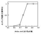
図3は、発明者が第2除去層105の除去のためにエッチング液として塩酸を使用したエッチング実験で確認したAlzGa1-zAsのエッチング速度と、AlzGa1-zAsの組成を定めるzの値との関係を示す図である。図3における縦軸は、z=1の時のエッチング速度を1とした場合の相対値である。図3の結果から、第1除去層104の組成をAlxGa1-xAs(0.6<x≦0.8)、第2除去層105の組成をAlyGa1-yAs(0.7<y≦1、y>x)とすることにより、第1除去層104のエッチング速度と第2除去層105のエッチング速度との間に大きな差がある第1除去層104及び第2除去層105の組合せを選択できることがわかる。
[半導体基板1の構成の変形例]
図1においては、除去層102が第1除去層104及び第2除去層105の2層を有する構造を例示したが、半導体基板1は、第1除去層104及び第2除去層105を含む2層の他に、他の除去層を有してもよい。この時、除去層102のベース基板101に接する側から半導体エピタキシャル層103に接する側に向けてエッチング速度が大きくなる順番に積層することが望ましい。
図1においては、除去層102が第1除去層104及び第2除去層105の2層を有する構造を例示したが、半導体基板1は、第1除去層104及び第2除去層105を含む2層の他に、他の除去層を有してもよい。この時、除去層102のベース基板101に接する側から半導体エピタキシャル層103に接する側に向けてエッチング速度が大きくなる順番に積層することが望ましい。
例えば、半導体基板1は、第1除去層104と第2除去層105との間に第3除去層をさらに有してもよい。この場合、使用エッチング材料に対する第3除去層のエッチング速度は、使用エッチング材料に対する第1除去層104のエッチング速度よりも大きく、使用エッチング材料に対する第2除去層105のエッチング速度よりも小さい。
なお、以上の説明においては、ベース基板101がGaAs基板である場合を例示したが、本発明は、ベース基板101が他のIII-V族半導体エピタキシャル基板である場合にも適用できる。半導体基板1は、例えば、ベース基板101がInP基板であり、半導体エピタキシャル層103がInP基板上で格子整合又は略格子整合する半導体エピタキシャル層(例えばIn1-xGaxAsyP1-y(0≦x、y≦1))であってもよい。この場合、除去層102は、InP基板上で格子整合又は略格子整合する半導体層であり、例えば、第1除去層104がIn0.52Al0.48Asであり、第2除去層105がIn0.53Ga0.47Asである。
[半導体素子の製造方法]
続いて、半導体エピタキシャル層103をベース基板101から分離した後に、他の基板に半導体エピタキシャル層103を移動させて半導体素子を製造する方法について説明する。
続いて、半導体エピタキシャル層103をベース基板101から分離した後に、他の基板に半導体エピタキシャル層103を移動させて半導体素子を製造する方法について説明する。
図4(図4Aから図4D)は、半導体素子の製造方法を説明するための図である。
まず、図1に示した半導体基板1を準備する。例えば、ベース基板101上に第1除去層104及び第2除去層105を含む積層構造を形成した後に、第2除去層105上に半導体エピタキシャル層103を形成することにより、半導体基板1を作製する。半導体エピタキシャル層103は、所定の素子を形成するための半導体積層構造を有する。所定の素子は、発光ダイオード、トランジスタ及びセンサー等のように、半導体により構成される任意の素子である。
まず、図1に示した半導体基板1を準備する。例えば、ベース基板101上に第1除去層104及び第2除去層105を含む積層構造を形成した後に、第2除去層105上に半導体エピタキシャル層103を形成することにより、半導体基板1を作製する。半導体エピタキシャル層103は、所定の素子を形成するための半導体積層構造を有する。所定の素子は、発光ダイオード、トランジスタ及びセンサー等のように、半導体により構成される任意の素子である。
なお、本製造方法においては、半導体基板1を作製する代わりに、作製済の半導体基板1を用いて半導体素子を製造してもよい。すなわち、ベース基板101上に第1除去層104、第2除去層105、及び半導体エピタキシャル層103が既に形成されている半導体基板1を準備する工程を半導体素子の製造方法の最初の工程としてもよい。また、半導体エピタキシャル層103に所定の素子構造または所定の素子構造の一部が既に形成されている半導体基板1を準備する工程を、半導体素子の製造方法の最初の工程としてもよい。
次に、図4Aに示すように、エッチングにより除去する第2除去層105の少なくとも一部(例えば外周面)が露出した島を形成する。例えば、半導体基板1における半導体エピタキシャル層103、第1除去層104及び第2除去層105の外周から所定の範囲をエッチングすることにより、図4Aに示す島を形成する。
続いて、図4Bに示すように、所定のエッチング液により第1除去層104及び第2除去層105をエッチングする。エッチング工程では、第2除去層105が完全に除去されるまでの間エッチングを継続し、第2除去層105が除去された時点でエッチングを停止する。このようにすることで、第2除去層105が完全に除去されたことにより空隙114が形成される。第1除去層104の第2除去層105の側の一部の領域(図4Bにおける領域113)が除去され、第1除去層104におけるベース基板101に接する側と反対側の面に凹凸が形成された粗面を有する第1除去層104の残留層117が形成される。なお、図4Bでは、形成された凹凸を誇張して描いている。
続いて、図4Cに示すように、例えばピックアップバンプ122を備えたピックアップ基板121を使って、半導体エピタキシャル層103をベース基板101から分離する。ピックアップバンプ122は、例えば有機材料層であり、半導体基板上に感光性有機材料を塗布して、標準的なフォトリソグラフィプロセスにより形成することができる。有機材料層は、例えば、スピンコート法、ディップ法などにより、ピックアップ基板121のベースとなるピックアップベース基板上に有機材料をコートすることにより形成してもよいし、有機材料フィルムをピックアップベース基板上に貼り付けることにより形成してもよい。
続いて、図4Dに示すように、ピックアップ基板121によりベース基板101から分離させた半導体エピタキシャル層103を移動先基板130の上に圧接して接合する。接合に先立って、接合面の活性化処理などの表面処理工程を実行してもよい。また、移動先基板130上に、移動先基板130の材料と異なる材料層として、例えば別の半導体層、金属層又は絶縁膜層を設けてもよい。
移動先基板130上に半導体エピタキシャル層103を接合した後に、ピックアップ基板121を分離する(図示せず)。ピックアップ基板121を分離した後の半導体エピタキシャル層103に、適宜、層間絶縁膜又は金属配線膜等を形成することにより、半導体素子の製造を完了する。
[第1変形例]
図4Aに示したように半導体エピタキシャル層103、第1除去層104及び第2除去層105を含む島をベース基板101上に形成した後に、半導体エピタキシャル層103がベース基板101の上方に位置するように半導体エピタキシャル層103を支持するための支持部材を設けてもよい。
図4Aに示したように半導体エピタキシャル層103、第1除去層104及び第2除去層105を含む島をベース基板101上に形成した後に、半導体エピタキシャル層103がベース基板101の上方に位置するように半導体エピタキシャル層103を支持するための支持部材を設けてもよい。
図5は、支持部材106を設けた例を示す図である。支持部材106は、例えば半導体エピタキシャル層103とベース基板101とを結合する半導体薄膜、有機材料薄膜、又は無機材料薄膜である。支持部材106は、例えば一部の領域が第1除去層104及び第2除去層105の側面に接するように形成されている。支持部材106の一部は、半導体エピタキシャル層103の上面又はベース基板101が露出した面に延在するように形成されていてもよい。当該支持部材106を構成する薄膜は、第2除去層105を除去する際に使用されるエッチング材料に対するエッチング速度が第2除去層105のエッチング速度よりも十分に小さく、第2除去層105が除去された時点で、半導体エピタキシャル層103とベース基板101とを結合した状態で残留する。
支持部材106は、例えば以下のようにして形成してもよい。アモルファスSi又はポリSiなどの半導体薄膜で支持部材106を形成する場合には、例えば、スパッタ法、熱CVD(Chemical Vapor Deposition)法、PCVD(Plasma Chemical Vapor Deposition)法、あるいはLPCVD(Low pressure Chemical Vapor Deposition)法などを適宜選択して半導体薄膜を形成することができる。この場合、半導体薄膜を形成後、フォトリソグラフィーおよびRIE(Reactive Ion Etching)法などのドライエッチング又は所定のエッチング液を使ったウェットエッチングによって支持部材106の構造を形成することができる。
無機材料薄膜で支持部材106を形成する場合には、例えばスパッタ法、熱CVD法、又はPCVD法などによって無機薄膜を形成することができる。無機薄膜を形成後、フォトリソグラフィー及びRIE法などのドライエッチング又は所定のエッチング液を使ったウェットエッチングによって支持部材106の構造を形成することができる。
有機材料薄膜で支持部材106を形成する場合には、例えば感光性有機材料を塗布又は貼付した後にフォトリソグラフィーによって所定の構造を形成し、その後、ベーク処理を行うことにより支持部材106を形成することができる。支持部材106の構造を形成する際に用いるエッチング液については、支持部材106のエッチング速度と比較して第1の除去層、第2の除去層、及び半導体エピタキシャル層103のエッチング速度が小さいエッチング液やエッチングガスを選択することが望ましい。
このように、第2除去層105を除去する工程において支持部材106が設けられることにより、半導体エピタキシャル層103が第1除去層104又はベース基板101と接触する確率を低くすることができる。特に、第2除去層105よりもエッチング速度が小さい第1除去層104が設けられていることにより、支持部材106を構成する薄膜が破損したり残留しない状態になったりした場合であっても、半導体エピタキシャル層103がベース基板101と接合してしまうことを防止できる。
なお、支持部材106は、半導体エピタキシャル層103がベース基板101から離れる向きに力が加わることで、容易に切断されるように形成されていることが好ましい。例えば、支持部材106が、第2除去層105の側面に接する領域の一部の厚みが他の領域の厚みよりも小さい形状(例えば溝の形状)を有することで、第2除去層105が除去された後に支持部材106は容易に切断される。この場合、所定のエッチング材料を用いてエッチングすることにより第2除去層105を除去する除去工程と、半導体エピタキシャル層103を101ベース基板と異なる移動先基板130に接合する接合工程との間に、半導体エピタキシャル層103を引き上げることにより支持部材106を切断する工程をさらに有してもよい。
所定領域の厚みが他の領域の厚みよりも小さい支持部材106は、例えば以下の方法により作製することができる。まず、厚みを小さくする領域(例えば溝を形状を形成する領域)以外の領域をレジストで被覆する。続いて、支持部材106の材料をエッチングするエッチング液を使ったウェットエッチング又はRIEなどのドライエッチングによって所定の厚さになるようにエッチングした後にレジストを除去する。
[第2変形例]
以上の説明においては、第1除去層104のエッチング速度よりも、上記の所定のエッチング材料に対する第2除去層105のエッチング速度が大きい場合を例示したが、第1除去層104のエッチング速度が第2除去層105のエッチング速度以上であってもよい。ただし、この場合、エッチングによる第2除去層105の除去が完了した時点で第1除去層104の少なくとも一部が残留しているように、第1除去層104の厚みを第2除去層105の厚みよりも大きくすることが求められる。
以上の説明においては、第1除去層104のエッチング速度よりも、上記の所定のエッチング材料に対する第2除去層105のエッチング速度が大きい場合を例示したが、第1除去層104のエッチング速度が第2除去層105のエッチング速度以上であってもよい。ただし、この場合、エッチングによる第2除去層105の除去が完了した時点で第1除去層104の少なくとも一部が残留しているように、第1除去層104の厚みを第2除去層105の厚みよりも大きくすることが求められる。
[半導体基板1による効果]
本発明の半導体基板1は、ベース基板101から分離する予定の半導体エピタキシャル層103とベース基板101との間に、エッチング速度が異なる少なくとも2層の除去層を有する。したがって、半導体エピタキシャル層103が分離された後に、半導体エピタキシャル層103がベース基板101と接合することを防止できる。
本発明の半導体基板1は、ベース基板101から分離する予定の半導体エピタキシャル層103とベース基板101との間に、エッチング速度が異なる少なくとも2層の除去層を有する。したがって、半導体エピタキシャル層103が分離された後に、半導体エピタキシャル層103がベース基板101と接合することを防止できる。
そして、半導体基板1を用いて半導体素子を製造することにより、平坦な面を有する半導体エピタキシャル層103を移動先基板130に容易に移動させ、移動後の半導体エピタキシャル層103を加工して、各種の半導体素子を製造することができる。
以上、本発明を実施の形態を用いて説明したが、本発明の技術的範囲は上記実施の形態に記載の範囲には限定されず、その要旨の範囲内で種々の変形及び変更が可能である。例えば、装置の分散・統合の具体的な実施の形態は、以上の実施の形態に限られず、その全部又は一部について、任意の単位で機能的又は物理的に分散・統合して構成することができる。また、複数の実施の形態の任意の組み合わせによって生じる新たな実施の形態も、本発明の実施の形態に含まれる。組み合わせによって生じる新たな実施の形態の効果は、もとの実施の形態の効果を合わせ持つ。
1 半導体基板
101 ベース基板
102 除去層
103 半導体エピタキシャル層
104 第1除去層
105 第2除去層
112 下面
115 上面
117 残留層
121 ピックアップ基板
122 ピックアップバンプ
130 移動先基板
101 ベース基板
102 除去層
103 半導体エピタキシャル層
104 第1除去層
105 第2除去層
112 下面
115 上面
117 残留層
121 ピックアップ基板
122 ピックアップバンプ
130 移動先基板
Claims (13)
- ベース基板と、
前記ベース基板上に設けられた第1除去層と、
前記第1除去層の上方に設けられた第2除去層と、
前記第2除去層の上方に設けられた半導体エピタキシャル層と、
を有し、
所定のエッチング材料に対する前記第2除去層のエッチング速度が、前記所定のエッチング材料に対する前記第1除去層のエッチング速度よりも大きい、
半導体基板。 - 前記第2除去層の厚みよりも前記第1除去層の厚みが大きい、
請求項1に記載の半導体基板。 - 前記所定のエッチング材料を用いたエッチングにより前記第2除去層が除去された時点で露出している前記第1除去層の表面が、前記半導体エピタキシャル層の前記第2除去層側の面よりも粗い、
請求項1又は2に記載の半導体基板。 - 前記ベース基板がGaAsにより構成されており、
前記半導体エピタキシャル層がAltGa1-tAs(0≦t≦1)により構成されており、
前記第1除去層がAlxGa1-xAs(0.6<x≦0.8)により構成されており、
前記第2除去層がAlyGa1-yAs(0.7<y≦1、y>x)により構成されている、
請求項1から3のいずれか一項に記載の半導体基板。 - 前記半導体エピタキシャル層がAltGa1-tAs(0≦t≦0.6)により構成されている、
請求項4に記載の半導体基板。 - 前記ベース基板がInPにより構成されており、
前記半導体エピタキシャル層がIn1-xGaxAsyP1-y(0≦x、y≦1)である、
請求項1から3のいずれか一項に記載の半導体基板。 - 前記第1除去層と前記第2除去層との間に設けられた第3除去層をさらに有し、
前記所定のエッチング材料に対する前記第3除去層のエッチング速度は、前記所定のエッチング材料に対する前記第1除去層のエッチング速度よりも大きく、前記所定のエッチング材料に対する前記第2除去層のエッチング速度よりも小さい、
請求項1から6のいずれか一項に記載の半導体基板。 - 前記半導体エピタキシャル層が前記ベース基板の上方に位置するように前記半導体エピタキシャル層を支持するための支持部材をさらに有する、
請求項1から7のいずれか一項に記載の半導体基板。 - 前記支持部材は、前記ベース基板、前記第1除去層、前記第2除去層及び前記半導体エピタキシャル層に接する、
請求項8に記載の半導体基板。 - 前記支持部材は、前記第2除去層に接する領域の一部の厚みが他の領域の厚みよりも小さい形状を有する、
請求項8又は9に記載の半導体基板。 - ベース基板を準備する工程と、
前記ベース基板上に第1除去層を形成する工程と、
前記第1除去層の上方に、所定のエッチング材料に対するエッチング速度が、前記所定のエッチング材料に対する前記第1除去層のエッチング速度よりも大きい第2除去層を形成する工程と、
前記第2除去層の上方に半導体エピタキシャル層を形成する工程と、
前記半導体エピタキシャル層を形成した後に、前記半導体エピタキシャル層が前記ベース基板の上方に位置するように前記半導体エピタキシャル層を支持するための支持部材を設ける工程と、
を有する、
半導体基板の製造方法。 - 請求項1に記載の半導体基板を準備する工程と、
前記所定のエッチング材料を用いてエッチングすることにより前記第2除去層を除去する除去工程と、
前記除去工程の後に、前記半導体エピタキシャル層を前記ベース基板と異なる移動先基板に接合する接合工程と、
を有する、半導体素子の製造方法。 - 前記半導体基板が、前記半導体エピタキシャル層が前記ベース基板の上方に位置するように前記半導体エピタキシャル層を支持するための支持部材をさらに有し、
前記除去工程と前記接合工程との間に、前記支持部材を切断する工程をさらに有する、
請求項12に記載の半導体素子の製造方法。
Priority Applications (4)
| Application Number | Priority Date | Filing Date | Title |
|---|---|---|---|
| CN201980076538.1A CN113169049B (zh) | 2018-12-10 | 2019-10-17 | 半导体基板及其制造方法以及半导体元件的制造方法 |
| JP2020559573A JP6836022B2 (ja) | 2018-12-10 | 2019-10-17 | 半導体基板、半導体基板の製造方法及び半導体素子の製造方法 |
| US17/330,369 US11894272B2 (en) | 2018-12-10 | 2021-05-25 | Semiconductor substrate, method for manufacturing semiconductor substrate and method for manufacturing semiconductor device |
| US18/536,188 US20240120238A1 (en) | 2018-12-10 | 2023-12-11 | Semiconductor substrate, method for manufacturing semiconductor substrate and method for manufacturing semiconductor device |
Applications Claiming Priority (2)
| Application Number | Priority Date | Filing Date | Title |
|---|---|---|---|
| JP2018-230683 | 2018-12-10 | ||
| JP2018230683 | 2018-12-10 |
Related Child Applications (1)
| Application Number | Title | Priority Date | Filing Date |
|---|---|---|---|
| US17/330,369 Continuation US11894272B2 (en) | 2018-12-10 | 2021-05-25 | Semiconductor substrate, method for manufacturing semiconductor substrate and method for manufacturing semiconductor device |
Publications (1)
| Publication Number | Publication Date |
|---|---|
| WO2020121649A1 true WO2020121649A1 (ja) | 2020-06-18 |
Family
ID=71077231
Family Applications (1)
| Application Number | Title | Priority Date | Filing Date |
|---|---|---|---|
| PCT/JP2019/040926 WO2020121649A1 (ja) | 2018-12-10 | 2019-10-17 | 半導体基板、半導体基板の製造方法及び半導体素子の製造方法 |
Country Status (5)
| Country | Link |
|---|---|
| US (2) | US11894272B2 (ja) |
| JP (2) | JP6836022B2 (ja) |
| CN (1) | CN113169049B (ja) |
| TW (2) | TWI743610B (ja) |
| WO (1) | WO2020121649A1 (ja) |
Citations (6)
| Publication number | Priority date | Publication date | Assignee | Title |
|---|---|---|---|---|
| JP2005019590A (ja) * | 2003-06-25 | 2005-01-20 | Oki Data Corp | 半導体装置の製造方法 |
| JP2006080305A (ja) * | 2004-09-09 | 2006-03-23 | Sharp Corp | 化合物半導体素子エピタキシャル成長基板、半導体素子およびそれらの製造方法 |
| JP2010504649A (ja) * | 2006-09-20 | 2010-02-12 | ザ ボード オブ トラスティーズ オブ ザ ユニヴァーシティー オブ イリノイ | 転写可能な半導体構造、デバイス、及びデバイスコンポーネントを作成するための剥離方法 |
| JP2013211355A (ja) * | 2012-03-30 | 2013-10-10 | Oki Data Corp | 3端子発光素子、3端子発光素子アレイ、プリントヘッドおよび画像形成装置 |
| WO2016079929A1 (ja) * | 2014-11-21 | 2016-05-26 | 信越半導体株式会社 | 発光素子及び発光素子の製造方法 |
| WO2018070120A1 (ja) * | 2016-10-12 | 2018-04-19 | 信越半導体株式会社 | 発光素子及び発光素子の製造方法 |
Family Cites Families (29)
| Publication number | Priority date | Publication date | Assignee | Title |
|---|---|---|---|---|
| JPH0646026Y2 (ja) | 1987-08-19 | 1994-11-24 | 沖電気工業株式会社 | メンブレンキ−ボ−ドの防塵構造 |
| JP2560601B2 (ja) * | 1993-03-12 | 1996-12-04 | 日本電気株式会社 | 元素半導体基板上の金属膜/化合物半導体積層構造の製造方法 |
| JP3377022B2 (ja) * | 1997-01-23 | 2003-02-17 | 日本電信電話株式会社 | ヘテロ接合型電界効果トランジスタの製造方法 |
| JP3371871B2 (ja) * | 1999-11-16 | 2003-01-27 | 日本電気株式会社 | 半導体装置の製造方法 |
| JP3716906B2 (ja) * | 2000-03-06 | 2005-11-16 | 日本電気株式会社 | 電界効果トランジスタ |
| KR100438895B1 (ko) * | 2001-12-28 | 2004-07-02 | 한국전자통신연구원 | 고전자 이동도 트랜지스터 전력 소자 및 그 제조 방법 |
| JP3813123B2 (ja) | 2002-12-25 | 2006-08-23 | 株式会社沖データ | 半導体装置及びledヘッド |
| JP2005191022A (ja) * | 2003-12-24 | 2005-07-14 | Matsushita Electric Ind Co Ltd | 電界効果トランジスタ及びその製造方法 |
| US7205176B2 (en) * | 2004-05-24 | 2007-04-17 | Taiwan Semiconductor Manufacturing Company | Surface MEMS mirrors with oxide spacers |
| US20060208265A1 (en) * | 2005-03-17 | 2006-09-21 | Hitachi Cable, Ltd. | Light emitting diode and light emitting diode array |
| JP4200389B2 (ja) * | 2007-02-22 | 2008-12-24 | セイコーエプソン株式会社 | 光素子 |
| JP4466668B2 (ja) | 2007-03-20 | 2010-05-26 | セイコーエプソン株式会社 | 半導体装置の製造方法 |
| JP2008270794A (ja) * | 2007-03-29 | 2008-11-06 | Matsushita Electric Ind Co Ltd | 半導体装置及びその製造方法 |
| JP4871973B2 (ja) | 2009-04-28 | 2012-02-08 | 株式会社沖データ | 半導体薄膜素子の製造方法並びに半導体ウエハ、及び、半導体薄膜素子 |
| JP2011249776A (ja) * | 2010-04-30 | 2011-12-08 | Sumitomo Chemical Co Ltd | 半導体基板、半導体基板の製造方法、電子デバイス、および電子デバイスの製造方法 |
| JP5893246B2 (ja) * | 2010-11-08 | 2016-03-23 | キヤノン株式会社 | 面発光レーザ及び面発光レーザアレイ、面発光レーザの製造方法及び面発光レーザアレイの製造方法、面発光レーザアレイを備えた光学機器 |
| JP2013183125A (ja) * | 2012-03-05 | 2013-09-12 | Sharp Corp | 化合物半導体素子エピタキシャル成長基板 |
| US9859112B2 (en) * | 2013-07-18 | 2018-01-02 | Taiwan Semiconductor Manufacturing Co., Ltd | Bonded semiconductor structures |
| WO2015109242A1 (en) * | 2014-01-16 | 2015-07-23 | The Board Of Trustees Of The University Of Illinois | Printing-based multi-junction, multi-terminal photovoltaic devices |
| KR102178828B1 (ko) * | 2014-02-21 | 2020-11-13 | 삼성전자 주식회사 | 멀티 나노와이어 트랜지스터를 포함하는 반도체 소자 |
| KR102282141B1 (ko) * | 2014-09-02 | 2021-07-28 | 삼성전자주식회사 | 반도체 발광소자 |
| US9299615B1 (en) * | 2014-12-22 | 2016-03-29 | International Business Machines Corporation | Multiple VT in III-V FETs |
| US9444019B1 (en) * | 2015-09-21 | 2016-09-13 | Epistar Corporation | Method for reusing a substrate for making light-emitting device |
| US9461159B1 (en) * | 2016-01-14 | 2016-10-04 | Northrop Grumman Systems Corporation | Self-stop gate recess etching process for semiconductor field effect transistors |
| US9685539B1 (en) * | 2016-03-14 | 2017-06-20 | International Business Machines Corporation | Nanowire isolation scheme to reduce parasitic capacitance |
| WO2019134075A1 (en) * | 2018-01-03 | 2019-07-11 | Xiamen Sanan Integrated Circuit Co., Ltd. | Consumer semiconductor laser |
| JP6431631B1 (ja) | 2018-02-28 | 2018-11-28 | 株式会社フィルネックス | 半導体素子の製造方法 |
| US10461154B1 (en) * | 2018-06-21 | 2019-10-29 | International Business Machines Corporation | Bottom isolation for nanosheet transistors on bulk substrate |
| US11087974B2 (en) * | 2018-10-08 | 2021-08-10 | The Regents Of The University Of Michigan | Preparation of compound semiconductor substrate for epitaxial growth via non-destructive epitaxial lift-off |
-
2019
- 2019-10-17 WO PCT/JP2019/040926 patent/WO2020121649A1/ja active Application Filing
- 2019-10-17 CN CN201980076538.1A patent/CN113169049B/zh active Active
- 2019-10-17 JP JP2020559573A patent/JP6836022B2/ja active Active
- 2019-12-04 TW TW108144217A patent/TWI743610B/zh active
- 2019-12-04 TW TW110133490A patent/TWI804977B/zh active
-
2021
- 2021-02-04 JP JP2021016416A patent/JP7441525B2/ja active Active
- 2021-05-25 US US17/330,369 patent/US11894272B2/en active Active
-
2023
- 2023-12-11 US US18/536,188 patent/US20240120238A1/en active Pending
Patent Citations (6)
| Publication number | Priority date | Publication date | Assignee | Title |
|---|---|---|---|---|
| JP2005019590A (ja) * | 2003-06-25 | 2005-01-20 | Oki Data Corp | 半導体装置の製造方法 |
| JP2006080305A (ja) * | 2004-09-09 | 2006-03-23 | Sharp Corp | 化合物半導体素子エピタキシャル成長基板、半導体素子およびそれらの製造方法 |
| JP2010504649A (ja) * | 2006-09-20 | 2010-02-12 | ザ ボード オブ トラスティーズ オブ ザ ユニヴァーシティー オブ イリノイ | 転写可能な半導体構造、デバイス、及びデバイスコンポーネントを作成するための剥離方法 |
| JP2013211355A (ja) * | 2012-03-30 | 2013-10-10 | Oki Data Corp | 3端子発光素子、3端子発光素子アレイ、プリントヘッドおよび画像形成装置 |
| WO2016079929A1 (ja) * | 2014-11-21 | 2016-05-26 | 信越半導体株式会社 | 発光素子及び発光素子の製造方法 |
| WO2018070120A1 (ja) * | 2016-10-12 | 2018-04-19 | 信越半導体株式会社 | 発光素子及び発光素子の製造方法 |
Also Published As
| Publication number | Publication date |
|---|---|
| US20210280467A1 (en) | 2021-09-09 |
| CN113169049B (zh) | 2022-07-05 |
| TW202147392A (zh) | 2021-12-16 |
| JP7441525B2 (ja) | 2024-03-01 |
| US11894272B2 (en) | 2024-02-06 |
| US20240120238A1 (en) | 2024-04-11 |
| JP6836022B2 (ja) | 2021-02-24 |
| JPWO2020121649A1 (ja) | 2021-02-15 |
| CN113169049A (zh) | 2021-07-23 |
| JP2021077909A (ja) | 2021-05-20 |
| TWI804977B (zh) | 2023-06-11 |
| TW202038301A (zh) | 2020-10-16 |
| TWI743610B (zh) | 2021-10-21 |
Similar Documents
| Publication | Publication Date | Title |
|---|---|---|
| TWI767788B (zh) | 工程基板結構 | |
| US7008860B2 (en) | Substrate manufacturing method | |
| JP5524817B2 (ja) | 薄いsoiデバイスの製造 | |
| US7491966B2 (en) | Semiconductor substrate and process for producing it | |
| US9570351B2 (en) | Reusable semiconductor substrates | |
| WO2002047156A1 (fr) | Procede de realisation d'une couche mince impliquant l'introduction d'especes gazeuses | |
| JP6511516B2 (ja) | ゲルマニウム・オン・インシュレータ基板の製造方法 | |
| TWI390631B (zh) | 製造薄膜裝置之方法 | |
| JP2013509697A (ja) | 半導体・オン・絶縁体型構造における応力の分布を制御するための方法およびこの方法に関連した構造 | |
| JP2000315807A (ja) | プレーナ・ヘテロ構造の製造方法 | |
| US10910258B2 (en) | Engineered substrate structure and method of manufacture | |
| US7514282B2 (en) | Patterned silicon submicron tubes | |
| JP2009224758A (ja) | 複合半導体基板とその製造方法 | |
| WO2020121649A1 (ja) | 半導体基板、半導体基板の製造方法及び半導体素子の製造方法 | |
| JP2001109136A (ja) | ステンシルマスク及びステンシルマスクの形成方法 | |
| US20050186757A1 (en) | Method for lift off GaN pseudomask epitaxy layer using wafer bonding way | |
| TWI588886B (zh) | 製造半導體裝置之方法 | |
| TWI241651B (en) | Semiconductor etch speed modification | |
| JP6473970B2 (ja) | 貼り合わせsoiウェーハの製造方法 | |
| US11929255B2 (en) | Method of high-density pattern forming | |
| JP7490960B2 (ja) | 製造方法 | |
| US20230317510A1 (en) | Method for bonding a first substrate at a surface having an elastic nanotopology | |
| TWI697958B (zh) | 用於蝕刻遮罩與鰭片結構形成之方法 | |
| TWI850134B (zh) | 工程基板結構之製造方法 | |
| JP2008034531A (ja) | 化合物半導体光素子を作製する方法 |
Legal Events
| Date | Code | Title | Description |
|---|---|---|---|
| 121 | Ep: the epo has been informed by wipo that ep was designated in this application |
Ref document number: 19896797 Country of ref document: EP Kind code of ref document: A1 |
|
| ENP | Entry into the national phase |
Ref document number: 2020559573 Country of ref document: JP Kind code of ref document: A |
|
| NENP | Non-entry into the national phase |
Ref country code: DE |
|
| 122 | Ep: pct application non-entry in european phase |
Ref document number: 19896797 Country of ref document: EP Kind code of ref document: A1 |