WO2020105113A1 - 半導体装置および半導体装置の製造方法 - Google Patents
半導体装置および半導体装置の製造方法Info
- Publication number
- WO2020105113A1 WO2020105113A1 PCT/JP2018/042801 JP2018042801W WO2020105113A1 WO 2020105113 A1 WO2020105113 A1 WO 2020105113A1 JP 2018042801 W JP2018042801 W JP 2018042801W WO 2020105113 A1 WO2020105113 A1 WO 2020105113A1
- Authority
- WO
- WIPO (PCT)
- Prior art keywords
- semiconductor device
- inspection
- semiconductor
- inspection wiring
- wiring
- Prior art date
- Legal status (The legal status is an assumption and is not a legal conclusion. Google has not performed a legal analysis and makes no representation as to the accuracy of the status listed.)
- Ceased
Links
Images






Classifications
-
- H—ELECTRICITY
- H10—SEMICONDUCTOR DEVICES; ELECTRIC SOLID-STATE DEVICES NOT OTHERWISE PROVIDED FOR
- H10W—GENERIC PACKAGES, INTERCONNECTIONS, CONNECTORS OR OTHER CONSTRUCTIONAL DETAILS OF DEVICES COVERED BY CLASS H10
- H10W42/00—Arrangements for protection of devices
- H10W42/121—Arrangements for protection of devices protecting against mechanical damage
-
- H—ELECTRICITY
- H10—SEMICONDUCTOR DEVICES; ELECTRIC SOLID-STATE DEVICES NOT OTHERWISE PROVIDED FOR
- H10D—INORGANIC ELECTRIC SEMICONDUCTOR DEVICES
- H10D12/00—Bipolar devices controlled by the field effect, e.g. insulated-gate bipolar transistors [IGBT]
- H10D12/411—Insulated-gate bipolar transistors [IGBT]
-
- H—ELECTRICITY
- H10—SEMICONDUCTOR DEVICES; ELECTRIC SOLID-STATE DEVICES NOT OTHERWISE PROVIDED FOR
- H10P—GENERIC PROCESSES OR APPARATUS FOR THE MANUFACTURE OR TREATMENT OF DEVICES COVERED BY CLASS H10
- H10P54/00—Cutting or separating of wafers, substrates or parts of devices
-
- H—ELECTRICITY
- H10—SEMICONDUCTOR DEVICES; ELECTRIC SOLID-STATE DEVICES NOT OTHERWISE PROVIDED FOR
- H10P—GENERIC PROCESSES OR APPARATUS FOR THE MANUFACTURE OR TREATMENT OF DEVICES COVERED BY CLASS H10
- H10P74/00—Testing or measuring during manufacture or treatment of wafers, substrates or devices
- H10P74/27—Structural arrangements therefor
- H10P74/273—Interconnections for measuring or testing, e.g. probe pads
-
- H—ELECTRICITY
- H10—SEMICONDUCTOR DEVICES; ELECTRIC SOLID-STATE DEVICES NOT OTHERWISE PROVIDED FOR
- H10P—GENERIC PROCESSES OR APPARATUS FOR THE MANUFACTURE OR TREATMENT OF DEVICES COVERED BY CLASS H10
- H10P74/00—Testing or measuring during manufacture or treatment of wafers, substrates or devices
- H10P74/27—Structural arrangements therefor
- H10P74/277—Circuits for electrically characterising or monitoring manufacturing processes, e.g. circuits in tested chips or circuits in testing wafers
-
- H—ELECTRICITY
- H10—SEMICONDUCTOR DEVICES; ELECTRIC SOLID-STATE DEVICES NOT OTHERWISE PROVIDED FOR
- H10W—GENERIC PACKAGES, INTERCONNECTIONS, CONNECTORS OR OTHER CONSTRUCTIONAL DETAILS OF DEVICES COVERED BY CLASS H10
- H10W42/00—Arrangements for protection of devices
-
- H—ELECTRICITY
- H10—SEMICONDUCTOR DEVICES; ELECTRIC SOLID-STATE DEVICES NOT OTHERWISE PROVIDED FOR
- H10D—INORGANIC ELECTRIC SEMICONDUCTOR DEVICES
- H10D12/00—Bipolar devices controlled by the field effect, e.g. insulated-gate bipolar transistors [IGBT]
- H10D12/411—Insulated-gate bipolar transistors [IGBT]
- H10D12/441—Vertical IGBTs
-
- H—ELECTRICITY
- H10—SEMICONDUCTOR DEVICES; ELECTRIC SOLID-STATE DEVICES NOT OTHERWISE PROVIDED FOR
- H10D—INORGANIC ELECTRIC SEMICONDUCTOR DEVICES
- H10D30/00—Field-effect transistors [FET]
- H10D30/60—Insulated-gate field-effect transistors [IGFET]
- H10D30/64—Double-diffused metal-oxide semiconductor [DMOS] FETs
- H10D30/66—Vertical DMOS [VDMOS] FETs
- H10D30/665—Vertical DMOS [VDMOS] FETs having edge termination structures
-
- H—ELECTRICITY
- H10—SEMICONDUCTOR DEVICES; ELECTRIC SOLID-STATE DEVICES NOT OTHERWISE PROVIDED FOR
- H10D—INORGANIC ELECTRIC SEMICONDUCTOR DEVICES
- H10D62/00—Semiconductor bodies, or regions thereof, of devices having potential barriers
- H10D62/10—Shapes, relative sizes or dispositions of the regions of the semiconductor bodies; Shapes of the semiconductor bodies
- H10D62/102—Constructional design considerations for preventing surface leakage or controlling electric field concentration
- H10D62/112—Constructional design considerations for preventing surface leakage or controlling electric field concentration for preventing surface leakage due to surface inversion layers, e.g. by using channel stoppers
-
- H—ELECTRICITY
- H10—SEMICONDUCTOR DEVICES; ELECTRIC SOLID-STATE DEVICES NOT OTHERWISE PROVIDED FOR
- H10W—GENERIC PACKAGES, INTERCONNECTIONS, CONNECTORS OR OTHER CONSTRUCTIONAL DETAILS OF DEVICES COVERED BY CLASS H10
- H10W72/00—Interconnections or connectors in packages
- H10W72/90—Bond pads, in general
- H10W72/921—Structures or relative sizes of bond pads
- H10W72/926—Multiple bond pads having different sizes
Definitions
- the present invention relates to a semiconductor device and a semiconductor device manufacturing method.
- a plurality of power chips formed in a matrix on a wafer are cut along a dicing line to separate the power chips into individual pieces. Be converted. During this dicing process, chipping or cracking may occur on the power chip. In the past, in order to detect chipping and cracking, visual inspection was performed with an optical microscope after dicing.
- Patent Document 1 discloses a semiconductor device and a semiconductor device inspection method capable of detecting cracks generated after dicing. Inspection wiring is provided on the outer periphery of the chip region of the semiconductor device. According to the inspection method, it is possible to detect cracks generated during dicing by measuring the resistance value of the inspection wiring.
- the effective area which is the area in which the current related to the switching operation flows, is large. This is because the larger the effective area is, the smaller the loss during energization is.
- the inspection wiring as shown in Patent Document 1 is provided in the invalid area existing around the effective area.
- the ineffective area is an area in which a current related to the switching operation of the power chip does not flow.
- the area of the invalid region increases in accordance with the area of the inspection wiring and the inspection pad connected to the inspection wiring.
- the chip size increases in response to the increase of the area of the ineffective area due to the arrangement of the inspection wiring.
- the present invention has been made to solve the above problems, and an object of the present invention is to provide a semiconductor device in which the area of inspection wiring for detecting chipping, cracks, etc. is narrowed.
- a semiconductor device includes, on a front surface, an effective region including a semiconductor element and an ineffective region provided around the effective region, and on a back surface, a semiconductor substrate including a back surface electrode and an outer periphery of the effective region.
- the inspection wiring provided in the ineffective region of the surface of the semiconductor substrate. Since one end of the inspection wiring is in contact with the semiconductor layer provided in the ineffective region of the front surface of the semiconductor substrate and electrically connected to the back surface electrode, the inspection wiring is electrically connected to the back surface electrode. It is connected to the.
- the present invention it is possible to provide a semiconductor device in which the area of inspection wiring for detecting chipping, cracks, etc. is narrowed.
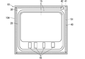
- FIG. 3 is a plan view showing the configuration of the semiconductor device according to the first embodiment.
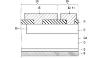
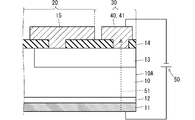
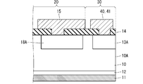
- FIG. 2 is a cross-sectional view showing the configuration of the semiconductor device taken along the line A-A ′ shown in FIG. 1.
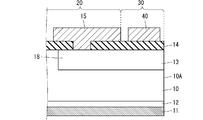
- FIG. 3 is a cross-sectional view showing the configuration of the semiconductor device taken along the line B-B ′ shown in FIG. 1.
- 6 is a flowchart showing a method for manufacturing the semiconductor device according to the first embodiment.
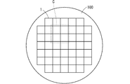
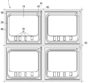
- FIG. 3 is a diagram showing a configuration of a semiconductor wafer according to the first embodiment. It is the figure which expanded the area
- FIG. 13 is a cross-sectional view showing the configuration of the semiconductor device according to the modification of the first embodiment.
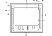
- FIG. 7 is a plan view showing the configuration of the semiconductor device according to the second embodiment.
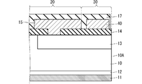
- FIG. 11 is a cross-sectional view showing the configuration of the semiconductor device at D-D ′ shown in FIG. 10.
- FIG. 11 is a cross-sectional view showing the configuration of the semiconductor device at E-E ′ shown in FIG. 10.
- FIG. 16 is a cross-sectional view showing the structure of the semiconductor device in the third embodiment.
- FIG. 16 is a cross-sectional view showing the structure of the semiconductor device in the third embodiment.
- FIG. 16 is a plan view showing the configuration of the semiconductor device according to the fourth embodiment.
- FIG. 16 is a cross-sectional view showing the structure of the semiconductor device at F-F ′ shown in FIG. 15.
- FIG. 1 is a plan view showing the configuration of the semiconductor device according to the first embodiment.
- FIG. 2 is a cross-sectional view showing the configuration of the semiconductor device along AA ′ shown in FIG.
- FIG. 3 is a cross-sectional view showing the configuration of the semiconductor device along BB ′ shown in FIG.
- the semiconductor device is composed of the semiconductor substrate 10 and the inspection wiring 40.
- the semiconductor substrate 10 includes an effective area 20 and an ineffective area 30.
- the invalid area 30 is provided around the effective area 20.
- the semiconductor substrate 10 includes semiconductor elements (not shown) in the effective area 20 on the surface. Further, in the effective area 20 on the surface of the semiconductor substrate 10, a main wiring 15 and a signal pad portion 16 for driving a semiconductor element are provided. The main wiring 15 and the signal pad section 16 are electrically connected to the semiconductor element in the effective region 20.
- the semiconductor element includes, for example, an IGBT (Insulated Gate Bipolar Transistor) and a MOSFET (Metal-Oxide-Semiconductor Field-Effect Transistor).
- the semiconductor substrate 10 contains Si or SiC.
- the semiconductor device is a power chip and switches a current flowing between a back electrode and a front electrode, which will be described later.
- the surface electrode corresponds to the main wiring 15.
- the above-mentioned effective region 20 corresponds to a region in which a current flows from the front surface to the back surface of the semiconductor substrate 10 according to the switching operation of the semiconductor element.
- the semiconductor substrate 10 includes a p-type semiconductor layer 12 on the back surface and a back surface electrode 11 provided on the p-type semiconductor layer 12.
- the back surface electrode 11 has a structure in which, for example, AlSi, Ti, Ni, Au, etc. are stacked.
- the back surface electrode 11 is a collector electrode.
- the semiconductor element is a MOSFET and the main wiring 15 is connected to the source electrode, the back surface electrode 11 is a drain electrode.
- the semiconductor substrate 10 also includes the n-type semiconductor layer 13 in the ineffective region 30 on the surface.
- the n-type semiconductor layer 13 is electrically connected to the back surface electrode 11 via the p-type semiconductor layer 12.
- the n-type semiconductor layer 13 is a layer extending from the channel stopper 18 provided on the outer periphery of the effective region 20.
- An insulating layer 14 is stacked on the n-type semiconductor layer 13 and the channel stopper 18.
- the insulating layer 14 is, for example, an oxide film. In the opening of the insulating layer 14 in the effective area 20, the main wiring 15 and the channel stopper 18 are in contact with each other.
- the inspection wiring 40 is provided in the ineffective region 30 on the surface of the semiconductor substrate 10 so as to surround the outer periphery of the effective region 20.
- the inspection wiring 40 is provided between the outer periphery of the effective area 20 and the outer edge portion 10A of the semiconductor substrate 10.
- the outer edge portion 10A corresponds to a dicing line defined in an invalid area 30 described later. Therefore, it can be said that the inspection wiring 40 is arranged between the channel stopper 18 and the dicing line.
- one end 41 of the inspection wiring 40 is in contact with the n-type semiconductor layer 13 at the opening of the insulating layer 14 in the ineffective region.
- the inspection wiring 40 is electrically connected to the back surface electrode 11 via the one end 41 and the n-type semiconductor layer 13.
- the inspection wiring 40 other than the one end 41 is insulated from the n-type semiconductor layer 13 by the insulating layer 14, as shown in FIG.
- the inspection wiring 40 includes an inspection pad 42 at the other end, as shown in FIG.
- the width of the inspection pad 42 is wider than the width of the wiring body extending from the one end 41 to the other end.
- the inspection wiring 40 includes, for example, aluminum.
- FIG. 4 is a flowchart showing the method of manufacturing the semiconductor device according to the first embodiment.
- step S1 a semiconductor wafer including a plurality of chips on the front surface and a back surface electrode 11 on the back surface is prepared.
- FIG. 5 is a diagram showing the configuration of the semiconductor wafer 100 according to the first embodiment.
- the plurality of chips 1 are arranged in a matrix on the surface of the semiconductor wafer 100.
- FIG. 6 is an enlarged view of the region C shown in FIG.
- Each of the plurality of chips 1 includes an effective region 20 including a semiconductor element and an ineffective region 30 provided around the effective region 20.
- the semiconductor wafer 100 includes a back surface electrode 11 on the back surface.
- the configuration of the semiconductor wafer 100 is the same as the configuration of the semiconductor substrate 10 described above, and the semiconductor wafer 100 in a state in which a plurality of chips 1 are separated into individual pieces corresponds to the semiconductor substrate 10 described above in the process described below.
- step S2 the inspection wiring 40 is formed so as to surround the outer periphery of the effective area 20 (see FIG. 6).
- the inspection wiring 40 is formed so that one end 41 contacts the n-type semiconductor layer 13 provided in the ineffective region 30 on the surface of the semiconductor wafer 100.
- step S3 the semiconductor wafer 100 is cut to divide the plurality of chips 1 into individual pieces.
- the semiconductor wafer 100 is cut along the dicing line 60.
- the dicing line 60 is defined in the invalid region 30 between the plurality of chips 1 adjacent to each other and located outside the inspection wiring 40 with respect to the valid region 20.
- the dicing line 60 after the plurality of chips 1 are singulated corresponds to the outer edge portion 10A of the semiconductor substrate 10 in FIG. That is, each of the plurality of individual chips 1 corresponds to one semiconductor device.
- step S4 the electrical connection state between the inspection wiring 40 and the back surface electrode 11 is inspected.
- a voltage is applied from the DC power supply 50 between the inspection wiring 40 and the back surface electrode 11 in each of the plurality of chips 1.
- FIG. 7 is a diagram showing a state in which a voltage is applied between the inspection wiring 40 and the back surface electrode 11.
- FIG. 8 is a diagram showing a current path 51 flowing from one end 41 of the inspection wiring 40 to the inspection pad 42. If chipping or cracks occur in the inspection wiring, the current value changes. Therefore, by measuring the current value in the current path 51, the inspection of the electrical connection state between the inspection wiring 40 and the back surface electrode 11 can be inspected.
- the semiconductor device includes the semiconductor substrate 10 and the inspection wiring 40.
- the semiconductor substrate 10 includes an effective region 20 including a semiconductor element on the front surface, an ineffective region 30 provided around the effective region 20, and a back surface electrode 11 on the back surface.
- the inspection wiring 40 is provided in the ineffective region 30 on the surface of the semiconductor substrate 10 so as to surround the outer periphery of the effective region 20. Since one end 41 of the inspection wiring 40 is in contact with a semiconductor layer provided in the ineffective region 30 of the surface of the semiconductor substrate 10 and electrically connected to the back electrode 11, the inspection wiring 40 Are electrically connected to the back surface electrode 11.
- the semiconductor layer is the n-type semiconductor layer 13.
- Such a semiconductor device makes it possible to detect chipping or cracks by measuring the current flowing from the back surface electrode 11 to the inspection wiring 40. Since the semiconductor device does not need a plurality of inspection pads for applying a voltage to the inspection wiring 40, the area of the inspection wiring 40 can be narrowed. Therefore, the area of the ineffective region 30 can be reduced while maintaining the area of the effective region 20. Therefore, the semiconductor device realizes cost reduction by reducing the chip size while reducing the loss during energization. Further, the semiconductor device can detect chipping or cracks on the dicing line, which cannot be detected by the conventional withstand voltage measurement. Further, when the semiconductor substrate contains a wide band gap semiconductor such as SiC, chipping or cracking is likely to occur due to its high hardness.
- the semiconductor device described in Embodiment 1 is suitable for detecting chipping or cracks in a wide band gap semiconductor.
- the inspection wiring 40 of the semiconductor device according to the first embodiment includes an inspection pad 42 at the other end.
- the width of the inspection pad 42 is wider than the width of the wiring body extending from the one end 41 to the other end.
- the area of the inspection wiring 40 can be narrowed.
- a voltage is applied between one end and the other end of the inspection wiring 40, instead of applying a voltage between the one end 41 of the inspection wiring 40 and the back surface electrode 11, a plurality of inspection wires are provided on the surface of the semiconductor device. Pads are needed.
- at least one inspection pad may be arranged on the surface of the semiconductor device. ..
- the inspection wiring 40 of the semiconductor device in the first embodiment contains aluminum.
- Such a semiconductor device makes it possible to form the inspection wiring 40 in the same manufacturing process as other aluminum wirings or aluminum electrode layers of the semiconductor device.
- the semiconductor element of the semiconductor device according to the first embodiment includes an IGBT, a MOSFET or a diode that controls a current flowing between the back surface electrode 11 and the front surface electrode provided in the effective region 20 on the surface of the semiconductor substrate 10.
- the surface electrode is the main wiring 15.
- Such a semiconductor device makes it possible to use the back surface electrode 11 of the semiconductor element as an electrode for applying a voltage to the inspection wiring 40.
- the surface includes effective regions 20 each including a semiconductor element, and ineffective regions 30 provided around effective region 20 and arranged in a matrix.
- a semiconductor wafer 100 including a plurality of chips 1 and a back surface electrode 11 on the back surface is prepared, and is a semiconductor layer provided in an ineffective region 30 on the front surface of the semiconductor wafer 100 and electrically connected to the back surface electrode 11.
- the inspection wiring 40 is formed in the ineffective region 30 on the surface of the semiconductor wafer 100 so that the one end 41 contacts the semiconductor layer (n-type semiconductor layer 13) and surrounds the outer periphery of the effective region 20, and the inspection wiring 40 is adjacent to each other.
- the semiconductor wafer 100 is cut along the dicing line 60 which is the invalid region 30 between the plurality of matching chips 1 and which is defined in the invalid region 30 outside the inspection wiring 40 with respect to the valid region 20 to thereby cut the plurality of chips. 1 is divided into individual pieces, and a voltage is applied between the inspection wiring 40 and the back surface electrode 11 in each of the plurality of chips 1 to detect a current flowing between the inspection wiring 40 and the back surface electrode 11. The electrical connection state between the inspection wiring 40 and the back surface electrode 11 is inspected.
- Such a method of manufacturing a semiconductor device makes it possible to detect chipping or cracks by measuring the current flowing from the back surface electrode 11 of the semiconductor device to the inspection wiring 40. Further, according to the method of manufacturing a semiconductor device, the semiconductor device does not require a plurality of inspection pads for applying a voltage to the inspection wiring 40, and thus the area of the inspection wiring 40 can be reduced. The area of the ineffective region 30 can be reduced while maintaining the area of the effective region 20. Therefore, the semiconductor device realizes cost reduction by reducing the chip size while reducing the loss during energization.
- the manufacturing method of the semiconductor device includes an inspection step of passing a current through the main wiring 15 and the back surface electrode 11 of the semiconductor device for the inspection of the semiconductor element
- the manufacturing method of the first embodiment includes the inspection step. Can be performed simultaneously or consecutively.
- the inspection device (not shown) is newly provided with one probe pin for applying a voltage to the inspection wiring 40 on the surface of the semiconductor device, and the inspection shown in the first embodiment is performed. Can be implemented.
- the method for manufacturing a semiconductor device makes it possible to detect chipping or cracks on a dicing line that cannot be detected by conventional withstand voltage measurement.
- the inspection wiring 40 includes an inspection pad 42 at the other end.
- the width of the inspection pad 42 is wider than the width of the wiring body extending from the one end 41 to the other end.
- Such a semiconductor device manufacturing method enables manufacturing of a semiconductor device in which the area of the inspection wiring 40 is narrowed.
- a voltage is applied between one end and the other end of the inspection wiring 40, instead of applying a voltage between the one end 41 of the inspection wiring 40 and the back surface electrode 11, a plurality of inspection wires are provided on the surface of the semiconductor device. Pads are needed.
- at least one inspection pad may be arranged on the surface of the semiconductor device. ..
- the inspection wiring 40 is formed between the outer periphery of the effective area 20 and the dicing line 60.
- Such a semiconductor device manufacturing method can detect the occurrence of chipping, cracks, or the like on the outer periphery of the semiconductor substrate 10.
- the inspection wiring 40 includes aluminum.
- Such a method for manufacturing a semiconductor device makes it possible to form the inspection wiring 40 in the same manufacturing process as other aluminum wirings or aluminum electrode layers (not shown) of the semiconductor device.
- the semiconductor element controls the current flowing between the back surface electrode 11 and the front surface electrode (main wiring 15) provided in the effective region 20 on the front surface of the semiconductor wafer 100.
- the semiconductor element controls the current flowing between the back surface electrode 11 and the front surface electrode (main wiring 15) provided in the effective region 20 on the front surface of the semiconductor wafer 100.
- the semiconductor element Including an IGBT, a MOSFET or a diode.
- Such a method of manufacturing a semiconductor device makes it possible to inspect a chipping or a crack by diverting the back surface electrode 11 of a semiconductor element into an electrode for applying a voltage to the inspection wiring 40.
- FIG. 9 is a cross-sectional view showing the configuration of the semiconductor device according to the modification of the first embodiment.
- FIG. 9 corresponds to the cross section of the semiconductor device taken along the line BB ′ shown in FIG.
- the inspection wiring 40A is thinner than the main wiring 15. Such a semiconductor device improves the sensitivity of chipping or crack detection.
- the inspection wiring 40A includes, for example, polysilicon.
- the inspection wiring 40A made of polysilicon facilitates formation of an inspection wiring thinner than the inspection wiring 40 made of aluminum shown in the first embodiment, for example. As a result, chipping or crack detection sensitivity is improved.
- FIG. 10 is a plan view showing the configuration of the semiconductor device according to the second embodiment.
- FIG. 11 is a cross-sectional view showing the structure of the semiconductor device at D-D 'shown in FIG.
- FIG. 12 is a cross-sectional view showing the structure of the semiconductor device at E-E 'shown in FIG.
- the semiconductor device according to the second embodiment further includes the protective film 17 that covers the inspection wiring 40 except for the inspection pad 42.
- the protective film 17 is formed between steps S2 and S3 shown in FIG.
- the protective film 17 prevents scratches or foreign matter from adhering to the inspection wiring 40. Therefore, the semiconductor device enables accurate detection of chipping or cracks caused by dicing.
- a semiconductor device and a method of manufacturing the semiconductor device according to the third embodiment will be described. Note that description of the same configuration and operation as in the first or second embodiment is omitted.
- the semiconductor device according to the third embodiment is different from the semiconductor device according to the first embodiment in the configuration of the n-type semiconductor layer in contact with the one end 41 of the inspection wiring 40.
- FIG. 13 and 14 are cross-sectional views showing the structure of the semiconductor device according to the third embodiment.
- FIG. 13 is a diagram corresponding to a cross section of the semiconductor device along the line A-A ′ shown in FIG. 1.
- FIG. 14 is a diagram corresponding to a cross section of the semiconductor device along line B-B ′ shown in FIG. 1.
- the n-type semiconductor layer 13A that is in contact with the one end 41 of the inspection wiring 40 is separated from the channel stopper 18A provided on the outer periphery of the effective region 20.
- the n-type semiconductor layer 13A is provided closer to the outer edge portion 10A of the semiconductor substrate 10 than the channel stopper 18A.
- the semiconductor wafer 100 including the channel stopper 18A and the n-type semiconductor layer 13A is prepared in step S1 shown in FIG.
- the inspection wiring 40 is provided between the channel stopper 18A and the outer edge portion 10A of the semiconductor substrate 10.
- the outer edge portion 10A corresponds to the dicing line 60 defined in the invalid area 30.
- Such an inspection wiring 40 is formed in step S2 shown in FIG.
- the semiconductor device having the above configuration can detect the occurrence of chipping or cracks on the outer periphery of the semiconductor substrate 10.
- the n-type semiconductor layer 13 in contact with the one end 41 of the inspection wiring 40 may be separated from the channel stopper 18 provided on the outer periphery of the effective region 20. Has the same effect.
- FIG. 15 is a plan view showing the configuration of the semiconductor device according to the fourth embodiment.
- 16 is a cross-sectional view showing the structure of the semiconductor device at F-F 'shown in FIG. 15 and 16 also show a current path 51 flowing from the back surface electrode 11 to the inspection pad 42 via the one end 41 of the inspection wiring 40.
- the semiconductor element included in the semiconductor device is a diode.
- the semiconductor substrate 10 includes an n-type semiconductor layer 19 on its back surface, and the back surface electrode 11 is provided on the n-type semiconductor layer 19.
- step S4 shown in FIG. 4 a voltage is applied between the inspection wiring 40 and the back surface electrode 11 by the DC power supply 50, and the back surface electrode 11 passes through one end 41 of the inspection wiring 40 to the inspection pad 42. An electric current flows. By detecting this current, the inspection of the electrical connection state between the inspection wiring 40 and the back surface electrode 11 can be inspected. Similar to the IGBT or MOSFET shown in other embodiments, chipping or cracks can be detected in a semiconductor device including a diode.
Landscapes
- Internal Circuitry In Semiconductor Integrated Circuit Devices (AREA)
- Testing Or Measuring Of Semiconductors Or The Like (AREA)
- Semiconductor Integrated Circuits (AREA)
- Engineering & Computer Science (AREA)
- Automation & Control Theory (AREA)
- Manufacturing & Machinery (AREA)
Abstract
チッピングまたはクラック等を検出する検査用配線の面積を狭小化する半導体装置の提供を目的とする。半導体装置は、表面には、半導体素子を含む有効領域と有効領域の周囲に設けられる無効領域とを含み、裏面には、裏面電極を含む半導体基板と、有効領域の外周を囲むように、半導体基板の表面の無効領域に設けられる検査用配線と、を含む。検査用配線の一端が半導体基板の表面の無効領域に設けられた半導体層であって裏面電極に電気的に接続された半導体層に接触していることにより、検査用配線は裏面電極に電気的に接続されている。
Description
本発明は、半導体装置および半導体装置の製造方法に関する。
IGBT(Insulated Gate Bipolar Transistor)、ダイオード等を含むパワーチップの製造工程においては、ウエハ上にマトリクス状に形成された複数のパワーチップがダイシングラインに沿って切断されることにより、パワーチップが個片化される。このダイシング工程の際、パワーチップにチッピングまたはクラックキングが発生することがある。従来は、チッピングやクラックキングの検出のため、ダイシング後に、光学顕微鏡による外観検査が実施されていた。
しかしながら、ウエハ径の拡大等に伴い検査時間が長時間化し、検査工程に費やすことができる時間の制約から、パワーチップの全数検査の実施が困難になってきている。また、チッピングまたはクラックキングが発生しているにも関わらず、光学顕微鏡の解像力の限界から、そのクラックやチッピングを検出できないこともある。
特許文献1には、ダイシング後に生じたクラックを検出することが可能な半導体装置および半導体装置の検査方法が開示されている。半導体装置のチップ領域の外周には、検査用配線が設けられている。その検査方法によれば、検査用配線の抵抗値を測定することにより、ダイシング時に発生するクラックを検出することが可能である。
チップ表面からチップ裏面に電流を流すパワーチップにおいては、スイッチング動作に関連する電流が流れる領域である有効領域の面積は大きいほうが好ましい。有効領域の面積が大きいほど、通電時の損失が低減するためである。
特許文献1に示されるような検査用配線は、有効領域の周囲に存在する無効領域に設けられる。無効領域とは、パワーチップのスイッチング動作に関連する電流が流れない領域である。検査用配線を有するパワーチップにおいて、無効領域の面積は、検査用配線およびその検査用配線に接続する検査用パッドの面積に応じて増加する。パワーチップの損失の低減ため有効領域の面積が維持された場合、検査用配線の配置による無効領域の面積増加に対応して、チップサイズが大きくなる。
本発明は、以上のような課題を解決するためになされたものであり、チッピングまたはクラック等を検出する検査用配線の面積を狭小化する半導体装置の提供を目的とする。
本発明に係る半導体装置は、表面には、半導体素子を含む有効領域と有効領域の周囲に設けられる無効領域とを含み、裏面には、裏面電極を含む半導体基板と、有効領域の外周を囲むように、半導体基板の表面の無効領域に設けられる検査用配線と、を含む。検査用配線の一端が半導体基板の表面の無効領域に設けられた半導体層であって裏面電極に電気的に接続された半導体層に接触していることにより、検査用配線は裏面電極に電気的に接続されている。
本発明によれば、チッピングまたはクラック等を検出する検査用配線の面積を狭小化する半導体装置の提供が可能である。
本発明の目的、特徴、局面、および利点は、以下の詳細な説明と添付図面とによって、より明白になる。
<実施の形態1>
図1は、実施の形態1における半導体装置の構成を示す平面図である。図2は、図1に示されるA-A’における半導体装置の構成を示す断面図である。図3は、図1に示されるB-B’における半導体装置の構成を示す断面図である。半導体装置は、半導体基板10と検査用配線40とで構成される。
図1は、実施の形態1における半導体装置の構成を示す平面図である。図2は、図1に示されるA-A’における半導体装置の構成を示す断面図である。図3は、図1に示されるB-B’における半導体装置の構成を示す断面図である。半導体装置は、半導体基板10と検査用配線40とで構成される。
半導体基板10は、有効領域20と無効領域30とを含む。無効領域30は、有効領域20の周囲に設けられる。半導体基板10は、表面の有効領域20に半導体素子(図示せず)を含む。さらに、半導体基板10の表面の有効領域20には、半導体素子を駆動させるためのメイン配線15および信号パッド部16が設けられている。メイン配線15および信号パッド部16は、有効領域20における半導体素子に電気的に接続されている。
半導体素子は、例えば、IGBT(Insulated Gate Bipolar Transistor)、MOSFET(Metal-Oxide-Semiconductor Field-Effect Transistor)を含む。半導体基板10は、SiまたはSiCを含む。実施の形態1において、半導体装置は、パワーチップであり、後述する裏面電極と表面電極との間に流れる電流をスイッチングする。ここでは、表面電極はメイン配線15に対応する。上述した有効領域20とは、半導体素子のスイッチング動作に応じて、半導体基板10の表面から裏面に電流が流れる領域に対応する。
半導体基板10は、図2に示されるように、裏面にp型半導体層12と、そのp型半導体層12上に設けられる裏面電極11とを含む。裏面電極11は、例えば、AlSi、Ti、Ni、Au等が積層された構造を有する。例えば、半導体素子がIGBTであってメイン配線15がエミッタ電極に接続される場合、裏面電極11はコレクタ電極である。例えば、半導体素子がMOSFETであってメイン配線15がソース電極に接続される場合、裏面電極11はドレイン電極である。
また、半導体基板10は、表面の無効領域30にn型半導体層13を含む。n型半導体層13は、p型半導体層12を介して裏面電極11に電気的に接続されている。実施の形態1において、n型半導体層13は、有効領域20の外周に設けられるチャネルストッパ18から延在する層である。また、n型半導体層13およびチャネルストッパ18上には、絶縁層14が積層されている。絶縁層14は、例えば酸化膜である。有効領域20における絶縁層14の開口において、メイン配線15とチャネルストッパ18とが接触している。
検査用配線40は、図1に示されるように、有効領域20の外周を囲むように、半導体基板10の表面の無効領域30に設けられている。検査用配線40は、有効領域20の外周と半導体基板10の外縁部10Aとの間に設けられる。外縁部10Aは、後述する無効領域30に定められるダイシングラインに対応する。そのため、検査用配線40はチャネルストッパ18とダイシングラインとの間に配置されているとも言える。
検査用配線40の一端41は、図2に示されるように、無効領域における絶縁層14の開口において、n型半導体層13に接触している。検査用配線40は、その一端41とn型半導体層13を介して裏面電極11に電気的に接続されている。また、一端41以外の検査用配線40は、図3に示されるように、絶縁層14によって、n型半導体層13とは絶縁されている。
また、検査用配線40は、図1に示されるように、他端に検査用パッド42を含む。検査用パッド42の幅は、一端41から他端に延在する配線本体の幅よりも広い。検査用配線40は、例えば、アルミニウムを含む。
図4は、実施の形態1における半導体装置の製造方法を示すフローチャートである。
ステップS1にて、表面に複数のチップを含み、裏面に裏面電極11を含む半導体ウエハを準備する。図5は、実施の形態1における半導体ウエハ100の構成を示す図である。複数のチップ1は、半導体ウエハ100の表面にマトリクス状に配置されている。図6は、図5に示された領域Cが拡大された図である。複数のチップ1の各々は、半導体素子を含む有効領域20と、有効領域20の周囲に設けられる無効領域30とを含む。また、図示は省略するが、半導体ウエハ100は、裏面に裏面電極11を含む。半導体ウエハ100の構成は、上述した半導体基板10の構成と同様であり、後述する工程において、複数のチップ1が個片化された状態における半導体ウエハ100が、上述した半導体基板10に対応する。
ステップS2にて、有効領域20の外周を囲むように検査用配線40を形成する(図6参照)。検査用配線40は、一端41が半導体ウエハ100の表面の無効領域30に設けられたn型半導体層13に接触するよう形成される。
ステップS3にて、半導体ウエハ100を切断し、複数のチップ1を個片化する。この際、半導体ウエハ100は、ダイシングライン60に沿って切断される。ダイシングライン60は、互いに隣り合う複数のチップ1の間の無効領域30であって有効領域20に対し検査用配線40の外側に位置する無効領域30に定められている。複数のチップ1が個片化された後のダイシングライン60は、図1における半導体基板10の外縁部10Aに対応する。すなわち、個片化された複数のチップ1の各々が、1つの半導体装置に対応する。
ステップS4にて、検査用配線40と裏面電極11との間の電気的接続状態を検査する。複数のチップ1の各々における検査用配線40と裏面電極11との間に、DC電源50によって電圧が印加される。図7は、検査用配線40と裏面電極11との間に電圧が印加された状態を示す図である。チッピングおよびクラックによって検査用配線40が断線していない場合、裏面電極11から検査用配線40の一端41を介して検査用パッド42に電流が流れる。図8は、検査用配線40の一端41から検査用パッド42に流れる電流経路51を示す図である。検査配線にチッピングまたはクラックが発生した場合、電流値が変動する。そのため、電流経路51における電流値を測定することにより、検査用配線40と裏面電極11との間の電気的接続状態の検査を検査することができる。
以上をまとめると、実施の形態1における半導体装置は、半導体基板10と検査用配線40とを含む。半導体基板10は、表面には、半導体素子を含む有効領域20と有効領域20の周囲に設けられる無効領域30とを含み、裏面には、裏面電極11を含む。検査用配線40は、有効領域20の外周を囲むように、半導体基板10の表面の無効領域30に設けられる。検査用配線40の一端41が半導体基板10の表面の無効領域30に設けられた半導体層であって裏面電極11に電気的に接続された半導体層に接触していることにより、検査用配線40は裏面電極11に電気的に接続されている。実施の形態1において半導体層は、n型半導体層13である。
このような半導体装置は、裏面電極11から検査用配線40に流れる電流を測定することにより、チッピングまたはクラック等を検出することを可能にする。半導体装置は、検査用配線40に電圧を印加するための複数の検査用パッドを必要としないため、検査用配線40の面積の狭小化を可能とする。ゆえに、有効領域20の面積は維持しながら、無効領域30の面積を狭小化するこができる。そのため、半導体装置は、通電時の損失を低減しながら、チップサイズの減少による低コスト化を実現する。また、半導体装置は、従来の耐圧測定では検出できないダイシングライン上のチッピングまたはクラックを検出可能にする。また、半導体基板がSiC等のワイドバンドギャップ半導体を含む場合、その高い硬度に起因してチッピングまたはクラックが生じやすい。実施の形態1に示された半導体装置は、ワイドバンドギャップ半導体のチッピングまたはクラックの検出に適している。
また、実施の形態1における半導体装置の検査用配線40は、他端に検査用パッド42を含む。検査用パッド42の幅は、一端41から他端に延在する配線本体の幅よりも広い。
このような半導体装置は、表面に複数の検査用パッドを必要としないため、検査用配線40の面積の狭小化を可能とする。検査用配線40の一端41と裏面電極11との間に電圧を印加するのではなく、検査用配線の一端と他端との間に電圧を印加する場合、半導体装置の表面に複数の検査用パッドが必要となる。しかし、実施の形態1においては、検査用配線40の一端41と裏面電極11との間に電圧を印加するため、半導体装置の表面には、少なくとも1つの検査用パッドが配置されていればよい。
また、実施の形態1における半導体装置の検査用配線40は、アルミニウムを含む。
このような半導体装置は、半導体装置が有する他のアルミニウム配線またはアルミニウム電極層と同じ製造工程で検査用配線40を形成することを可能にする。
また、実施の形態1における半導体装置の半導体素子は、裏面電極11と、半導体基板10の表面における有効領域20に設けられる表面電極との間に流れる電流を制御するIGBT、MOSFETまたはダイオードを含む。実施の形態1において表面電極はメイン配線15である。
このような半導体装置は、半導体素子の裏面電極11を、検査用配線40に電圧を印加するための電極に流用することを可能にする。
また、実施の形態1における半導体装置の製造方法は、表面には、各々が半導体素子を含む有効領域20と有効領域20の周囲に設けられる無効領域30とを含み、かつマトリクス状に配置される複数のチップ1を含み、裏面には裏面電極11を含む半導体ウエハ100を準備し、半導体ウエハ100の表面の無効領域30に設けられた半導体層であって裏面電極11に電気的に接続された半導体層(n型半導体層13)に一端41が接触するように、かつ、有効領域20の外周を囲むように、半導体ウエハ100の表面の無効領域30に検査用配線40を形成し、互いに隣り合う複数のチップ1の間の無効領域30であって有効領域20に対し検査用配線40の外側における無効領域30に定められるダイシングライン60に沿って、半導体ウエハ100を切断して、複数のチップ1を個片化し、複数のチップ1の各々における検査用配線40と裏面電極11との間に電圧を印加して、検査用配線40と裏面電極11との間に流れる電流を検出することにより、検査用配線40と裏面電極11との間の電気的接続状態を検査する。
このような半導体装置の製造方法は、半導体装置の裏面電極11から検査用配線40に流れる電流を測定することによりチッピングまたはクラック等を検出することを可能にする。また、半導体装置の製造方法によれば、半導体装置は、検査用配線40に電圧を印加するための複数の検査用パッドを必要しないため、検査用配線40の面積の狭小化を可能とする。有効領域20の面積は維持しながら、無効領域30の面積を狭小化することができる。そのため、半導体装置は、通電時の損失を低減しながら、チップサイズの減少による低コスト化を実現する。
また、半導体装置の製造方法に、半導体素子の検査のために半導体装置のメイン配線15と裏面電極11とに電流を流す検査工程が含まれる場合、実施の形態1の製造方法は、その検査工程と同時または連続して行うことができる。その際、検査装置(図示せず)は、半導体装置の表面の検査用配線40に電圧を印加するための1本のプローブピンを新たに備えるだけで、実施の形態1に示された検査を実施することができる。半導体装置の製造方法は、従来の耐圧測定では検出できないダイシングライン上のチッピングまたはクラックを検出可能にする。
また、実施の形態1における半導体装置の製造方法において、検査用配線40は、他端に検査用パッド42を含む。検査用パッド42の幅は、一端41から他端に延在する配線本体の幅よりも広い。検査用パッド42と裏面電極11との間に電圧を印加することにより、検査用配線40と裏面電極11との間の電気的接続状態を検査する。
このような半導体装置の製造方法は、検査用配線40の面積が狭小化された半導体装置の製造を可能とする。検査用配線40の一端41と裏面電極11との間に電圧を印加するのではなく、検査用配線の一端と他端との間に電圧を印加する場合、半導体装置の表面に複数の検査用パッドが必要となる。しかし、実施の形態1においては、検査用配線40の一端41と裏面電極11との間に電圧を印加するため、半導体装置の表面には、少なくとも1つの検査用パッドが配置されていればよい。
また、実施の形態1における半導体装置の製造方法において、検査用配線40は、有効領域20の外周とダイシングライン60との間に形成される。
このような半導体装置の製造方法は、半導体基板10の外周におけるチッピングまたはクラック等の発生を検出することができる。
また、実施の形態1における半導体装置の製造方法において、検査用配線40は、アルミニウムを含む。
このような半導体装置の製造方法は、半導体装置が有する他のアルミニウム配線またはアルミニウム電極層(いずれも図示せず)と同じ製造工程で検査用配線40を形成することを可能にする。
また、実施の形態1における半導体装置の製造方法において、半導体素子は、裏面電極11と、半導体ウエハ100の表面における有効領域20に設けられる表面電極(メイン配線15)との間に流れる電流を制御するIGBT、MOSFETまたはダイオードを含む。
このような半導体装置の製造方法は、半導体素子の裏面電極11を、検査用配線40に電圧を印加するための電極に流用して、チッピングまたはクラックの検査を行うことを可能にする。
(実施の形態1の変形例)
実施の形態1の変形例における半導体装置において、検査用配線以外の構成は、実施の形態1の構成と同様である。図9は、実施の形態1の変形例における半導体装置の構成を示す断面図である。図9は、図1に示されたB-B’における半導体装置の断面に対応する。
実施の形態1の変形例における半導体装置において、検査用配線以外の構成は、実施の形態1の構成と同様である。図9は、実施の形態1の変形例における半導体装置の構成を示す断面図である。図9は、図1に示されたB-B’における半導体装置の断面に対応する。
実施の形態1の変形例において、検査用配線40Aの厚さは、メイン配線15の厚さよりも薄い。このような半導体装置は、チッピングまたはクラックの検出感度を向上させる。
また、検査用配線40Aは、例えば、ポリシリコンを含む。ポリシリコン製の検査用配線40Aは、例えば実施の形態1において示されたアルミニウム製の検査用配線40よりも薄い検査用配線の形成を容易にする。その結果、チッピングまたはクラックの検出感度が向上する。
<実施の形態2>
実施の形態2における半導体装置および半導体装置の製造方法を説明する。なお、実施の形態1と同様の構成および動作については説明を省略する。
実施の形態2における半導体装置および半導体装置の製造方法を説明する。なお、実施の形態1と同様の構成および動作については説明を省略する。
図10は、実施の形態2における半導体装置の構成を示す平面図である。図11は、図10に示されるD-D’における半導体装置の構成を示す断面図である。図12は、図10に示されるE-E’における半導体装置の構成を示す断面図である。
実施の形態2における半導体装置は、検査用パッド42を除いて検査用配線40を覆っている保護膜17をさらに含む。保護膜17は、図4に示されるステップS2とS3との間において形成される。
保護膜17は、検査用配線40にキズまたは異物が付着することを防ぐ。そのため、半導体装置は、ダイシングによって生じるチッピングまたはクラックを精度よく検出することを可能にする。
<実施の形態3>
実施の形態3における半導体装置および半導体装置の製造方法を説明する。なお、実施の形態1または2と同様の構成および動作については説明を省略する。実施の形態3における半導体装置は、検査用配線40の一端41と接触しているn型半導体層の構成が、実施の形態1における半導体装置とは異なる。
実施の形態3における半導体装置および半導体装置の製造方法を説明する。なお、実施の形態1または2と同様の構成および動作については説明を省略する。実施の形態3における半導体装置は、検査用配線40の一端41と接触しているn型半導体層の構成が、実施の形態1における半導体装置とは異なる。
図13および図14は、実施の形態3における半導体装置の構成を示す断面図である。図13は、図1に示されるA-A’における半導体装置の断面に対応する図である。図14は、図1に示されるB-B’における半導体装置の断面に対応する図である。
実施の形態3における半導体装置において、検査用配線40の一端41と接触しているn型半導体層13Aは、有効領域20の外周に設けられるチャネルストッパ18Aとは分離されている。そのn型半導体層13Aは、チャネルストッパ18Aよりも半導体基板10の外縁部10Aの近くに設けられる。このようなチャネルストッパ18Aおよびn型半導体層13Aを含む半導体ウエハ100は、図4に示されるステップS1で準備される。
検査用配線40は、チャネルストッパ18Aと半導体基板10の外縁部10Aとの間に設けられる。外縁部10Aは、無効領域30に定められるダイシングライン60に対応する。このような検査用配線40は、図4に示されるステップS2で形成される。
以上のような構成を有する半導体装置は、半導体基板10の外周におけるチッピングまたはクラック等の発生を検出することができる。実施の形態2における半導体装置において、検査用配線40の一端41と接触しているn型半導体層13が、有効領域20の外周に設けられるチャネルストッパ18と分離されていてもよい。同様の効果を奏する。
<実施の形態4>
実施の形態4における半導体装置および半導体装置の製造方法を説明する。なお、実施の形態1から3のいずれかと同様の構成および動作については説明を省略する。
実施の形態4における半導体装置および半導体装置の製造方法を説明する。なお、実施の形態1から3のいずれかと同様の構成および動作については説明を省略する。
図15は、実施の形態4における半導体装置の構成を示す平面図である。図16は、図15に示されるF-F’における半導体装置の構成を示す断面図である。また、図15および図16は、裏面電極11から検査用配線40の一端41を介して検査用パッド42に流れる電流経路51も示している。
実施の形態4において、半導体装置が含む半導体素子は、ダイオードである。半導体基板10は、裏面にn型半導体層19を含み、裏面電極11は、そのn型半導体層19上に設けられている。
図4に示されるステップS4にて、検査用配線40と裏面電極11との間にDC電源50によって電圧が印加され、裏面電極11から検査用配線40の一端41を介して検査用パッド42に電流が流れる。この電流を検出することにより、検査用配線40と裏面電極11との間の電気的接続状態の検査を検査することができる。他の実施の形態に示されたIGBTまたはMOSFETと同様に、ダイオードを含む半導体装置においても、チッピングまたはクラックを検出することができる。
なお、本発明は、その発明の範囲内において、各実施の形態を自由に組み合わせたり、各実施の形態を適宜、変形、省略したりすることが可能である。
本発明は詳細に説明されたが、上記した説明は、全ての局面において、例示であって、本発明がそれに限定されるものではない。例示されていない無数の変形例が、この発明の範囲から外れることなく想定され得るものと解される。
1 チップ、10 半導体基板、10A 外縁部、11 裏面電極、13 n型半導体、15 メイン配線、16 信号パッド部、17 保護膜、18 チャネルストッパ、19 n型半導体層、20 有効領域、30 無効領域、40 検査用配線、41 一端、42 検査用パッド、60 ダイシングライン、100 半導体ウエハ。
Claims (16)
- 表面には、半導体素子を含む有効領域と前記有効領域の周囲に設けられる無効領域とを含み、裏面には、裏面電極を含む半導体基板と、
前記有効領域の外周を囲むように、前記半導体基板の前記表面の前記無効領域に設けられる検査用配線と、を備え、
前記検査用配線の一端が前記半導体基板の前記表面の前記無効領域に設けられた半導体層であって前記裏面電極に電気的に接続された前記半導体層に接触していることにより、前記検査用配線は前記裏面電極に電気的に接続されている、半導体装置。 - 前記検査用配線は、他端に検査用パッドを含み、
前記検査用パッドの幅は、前記一端から前記他端に延在する配線本体の幅よりも広い、請求項1に記載の半導体装置。 - 前記検査用配線は、前記有効領域の前記外周に設けられるチャネルストッパと前記半導体基板の外縁部との間に設けられ、
前記外縁部は、前記無効領域に定められるダイシングラインに対応する、請求項1または請求項2に記載の半導体装置。 - 前記検査用配線の厚さは、前記有効領域における前記半導体素子に接続されている配線の厚さよりも薄い、請求項1から請求項3のいずれか一項に記載の半導体装置。
- 前記検査用配線は、アルミニウムを含む、請求項1から請求項4のいずれか一項に記載の半導体装置。
- 前記検査用配線は、ポリシリコンを含む、請求項1から請求項5のいずれか一項に記載の半導体装置。
- 前記検査用パッドを除いて前記検査用配線を覆っている保護膜をさらに備える、請求項2に記載の半導体装置。
- 前記半導体素子は、前記裏面電極と、前記半導体基板の前記表面における前記有効領域に設けられる表面電極との間に流れる電流を制御するIGBT(Insulated Gate Bipolar Transistor)、MOSFET(Metal-Oxide-Semiconductor Field-Effect Transistor)またはダイオードを含む、請求項1から請求項7のいずれか一項に記載の半導体装置。
- 表面には、各々が半導体素子を含む有効領域と前記有効領域の周囲に設けられる無効領域とを含みかつマトリクス状に配置される複数のチップを含み、裏面には裏面電極を含む半導体ウエハを準備し、
前記半導体ウエハの前記表面の前記無効領域に設けられた半導体層であって前記裏面電極に電気的に接続された前記半導体層に一端が接触するように、かつ、前記有効領域の外周を囲むように、前記半導体ウエハの前記表面の前記無効領域に検査用配線を、形成し、
互いに隣り合う前記複数のチップの間の前記無効領域であって前記有効領域に対し前記検査用配線の外側における前記無効領域に定められるダイシングラインに沿って、前記半導体ウエハを切断して、前記複数のチップを個片化し、
前記複数のチップの各々における前記検査用配線と前記裏面電極との間に電圧を印加して、前記検査用配線と前記裏面電極との間に流れる電流を検出することにより、前記検査用配線と前記裏面電極との間の電気的接続状態を検査する、半導体装置の製造方法。 - 前記検査用配線は、他端に検査用パッドを含み、
前記検査用パッドの幅は、前記一端から前記他端に延在する配線本体の幅よりも広く、
前記検査用パッドと前記裏面電極との間に前記電圧を印加することにより、前記検査用配線と前記裏面電極との間の前記電気的接続状態を検査する、請求項9に記載の半導体装置の製造方法。 - 前記検査用配線は、前記有効領域の前記外周に設けられるチャネルストッパと前記ダイシングラインとの間に形成される、請求項9または請求項10に記載の半導体装置の製造方法。
- 前記検査用配線の厚さは、前記有効領域における前記半導体素子に接続されている配線の厚さよりも薄い、請求項9から請求項11のいずれか一項に記載の半導体装置の製造方法。
- 前記検査用配線は、アルミニウムを含む、請求項9から請求項12のいずれか一項に記載の半導体装置の製造方法。
- 前記検査用配線は、ポリシリコンを含む、請求項9から請求項13のいずれか一項に記載の半導体装置の製造方法。
- 前記検査用パッドを除いて前記検査用配線を覆う保護膜をさらに形成する、請求項10に記載の半導体装置の製造方法。
- 前記半導体素子は、前記裏面電極と、前記半導体ウエハの前記表面における前記有効領域に設けられる表面電極との間に流れる電流を制御するIGBT、MOSFETまたはダイオードを含む、請求項9から請求項15のいずれか一項に記載の半導体装置の製造方法。
Priority Applications (5)
| Application Number | Priority Date | Filing Date | Title |
|---|---|---|---|
| PCT/JP2018/042801 WO2020105113A1 (ja) | 2018-11-20 | 2018-11-20 | 半導体装置および半導体装置の製造方法 |
| JP2020557061A JP7109581B2 (ja) | 2018-11-20 | 2018-11-20 | 半導体装置および半導体装置の製造方法 |
| US17/275,165 US12148712B2 (en) | 2018-11-20 | 2018-11-20 | Semiconductor device and method of manufacturing semiconductor device |
| DE112018008153.2T DE112018008153T5 (de) | 2018-11-20 | 2018-11-20 | Halbleitervorrichtung und Verfahren zum Herstellen einer Halbleitervorrichtung |
| CN201880099521.3A CN113039630B (zh) | 2018-11-20 | 2018-11-20 | 半导体装置以及半导体装置的制造方法 |
Applications Claiming Priority (1)
| Application Number | Priority Date | Filing Date | Title |
|---|---|---|---|
| PCT/JP2018/042801 WO2020105113A1 (ja) | 2018-11-20 | 2018-11-20 | 半導体装置および半導体装置の製造方法 |
Publications (1)
| Publication Number | Publication Date |
|---|---|
| WO2020105113A1 true WO2020105113A1 (ja) | 2020-05-28 |
Family
ID=70773378
Family Applications (1)
| Application Number | Title | Priority Date | Filing Date |
|---|---|---|---|
| PCT/JP2018/042801 Ceased WO2020105113A1 (ja) | 2018-11-20 | 2018-11-20 | 半導体装置および半導体装置の製造方法 |
Country Status (5)
| Country | Link |
|---|---|
| US (1) | US12148712B2 (ja) |
| JP (1) | JP7109581B2 (ja) |
| CN (1) | CN113039630B (ja) |
| DE (1) | DE112018008153T5 (ja) |
| WO (1) | WO2020105113A1 (ja) |
Families Citing this family (1)
| Publication number | Priority date | Publication date | Assignee | Title |
|---|---|---|---|---|
| NL2036992B1 (en) * | 2024-02-08 | 2025-08-20 | Ampleon Netherlands Bv | Die crack detection system |
Citations (5)
| Publication number | Priority date | Publication date | Assignee | Title |
|---|---|---|---|---|
| JPS6376340A (ja) * | 1986-09-18 | 1988-04-06 | Oki Electric Ind Co Ltd | 集積回路チツプの外周部の欠陥検出装置 |
| JPH03209874A (ja) * | 1990-01-12 | 1991-09-12 | Hitachi Ltd | 半導体集積回路装置 |
| JP2000114516A (ja) * | 1998-10-02 | 2000-04-21 | Toshiba Corp | 半導体装置およびその製造方法 |
| JP2005277338A (ja) * | 2004-03-26 | 2005-10-06 | Nec Electronics Corp | 半導体装置及びその検査方法 |
| JP2010092924A (ja) * | 2008-10-03 | 2010-04-22 | Sharp Corp | 半導体装置及び半導体装置検査方法 |
Family Cites Families (10)
| Publication number | Priority date | Publication date | Assignee | Title |
|---|---|---|---|---|
| JPH06244254A (ja) * | 1993-02-22 | 1994-09-02 | Hitachi Ltd | 半導体集積回路素子 |
| JPH10329874A (ja) | 1997-05-28 | 1998-12-15 | Yoshino Kogyosho Co Ltd | 二種収納物混合容器 |
| JP2010177454A (ja) * | 2009-01-29 | 2010-08-12 | Sanyo Electric Co Ltd | 絶縁ゲート型半導体装置 |
| JP5777319B2 (ja) * | 2010-10-27 | 2015-09-09 | 三菱電機株式会社 | 半導体装置 |
| JP2012227210A (ja) | 2011-04-15 | 2012-11-15 | Fujikura Ltd | 電子部品、電子部品の製造方法、基板 |
| US9343381B2 (en) | 2013-05-22 | 2016-05-17 | Infineon Technologies Ag | Semiconductor component with integrated crack sensor and method for detecting a crack in a semiconductor component |
| WO2015040712A1 (ja) * | 2013-09-19 | 2015-03-26 | 三菱電機株式会社 | 半導体装置 |
| JP2015126084A (ja) * | 2013-12-26 | 2015-07-06 | トヨタ自動車株式会社 | 半導体装置 |
| JP6769165B2 (ja) * | 2016-08-10 | 2020-10-14 | 富士電機株式会社 | 半導体装置 |
| JP6702911B2 (ja) | 2017-04-21 | 2020-06-03 | 三菱電機株式会社 | 半導体装置およびその製造方法 |
-
2018
- 2018-11-20 DE DE112018008153.2T patent/DE112018008153T5/de active Pending
- 2018-11-20 US US17/275,165 patent/US12148712B2/en active Active
- 2018-11-20 JP JP2020557061A patent/JP7109581B2/ja active Active
- 2018-11-20 WO PCT/JP2018/042801 patent/WO2020105113A1/ja not_active Ceased
- 2018-11-20 CN CN201880099521.3A patent/CN113039630B/zh active Active
Patent Citations (5)
| Publication number | Priority date | Publication date | Assignee | Title |
|---|---|---|---|---|
| JPS6376340A (ja) * | 1986-09-18 | 1988-04-06 | Oki Electric Ind Co Ltd | 集積回路チツプの外周部の欠陥検出装置 |
| JPH03209874A (ja) * | 1990-01-12 | 1991-09-12 | Hitachi Ltd | 半導体集積回路装置 |
| JP2000114516A (ja) * | 1998-10-02 | 2000-04-21 | Toshiba Corp | 半導体装置およびその製造方法 |
| JP2005277338A (ja) * | 2004-03-26 | 2005-10-06 | Nec Electronics Corp | 半導体装置及びその検査方法 |
| JP2010092924A (ja) * | 2008-10-03 | 2010-04-22 | Sharp Corp | 半導体装置及び半導体装置検査方法 |
Also Published As
| Publication number | Publication date |
|---|---|
| JPWO2020105113A1 (ja) | 2021-04-30 |
| DE112018008153T5 (de) | 2021-08-05 |
| CN113039630B (zh) | 2024-09-17 |
| US20220045018A1 (en) | 2022-02-10 |
| JP7109581B2 (ja) | 2022-07-29 |
| CN113039630A (zh) | 2021-06-25 |
| US12148712B2 (en) | 2024-11-19 |
Similar Documents
| Publication | Publication Date | Title |
|---|---|---|
| US9761663B2 (en) | Semiconductor device | |
| JP6351547B2 (ja) | 電力用半導体装置および電力用半導体装置の製造方法 | |
| JP7294036B2 (ja) | 半導体試験装置、半導体装置の試験方法および半導体装置の製造方法 | |
| JP2013183143A (ja) | 半導体装置を製造する方法、及び、半導体装置 | |
| JP2018157192A (ja) | 半導体装置 | |
| WO2015136603A1 (ja) | パワー半導体モジュール及びその製造検査方法 | |
| JP7109581B2 (ja) | 半導体装置および半導体装置の製造方法 | |
| KR102210779B1 (ko) | 복수의 게이트 패드를 갖는 반도체 디바이스 | |
| JP7729033B2 (ja) | 炭化珪素半導体装置、半導体パッケージおよび炭化珪素半導体装置の検査方法 | |
| JP6135528B2 (ja) | 半導体装置の製造方法 | |
| US11531053B2 (en) | Semiconductor device and crack detection method | |
| JP2001053275A (ja) | 半導体装置およびその製造方法 | |
| WO2014045989A1 (ja) | 半導体ウェハ、半導体装置および半導体装置の製造方法 | |
| CN109979838B (zh) | 半导体器件以及检测半导体器件的裂纹的方法 | |
| JPH0817884A (ja) | 半導体装置およびその測定方法 | |
| JP5861822B2 (ja) | 半導体装置およびその試験方法 | |
| JPH02111044A (ja) | 半導体装置 | |
| JP2013105937A (ja) | 半導体装置及びその製造方法 | |
| JP2585556B2 (ja) | 半導体集積回路装置 | |
| JPH11345885A (ja) | 半導体装置 | |
| JP5266899B2 (ja) | 絶縁ゲート型バイポーラトランジスタの検査方法 | |
| JP2008141111A (ja) | 半導体装置及び半導体装置のチップクラック検査方法 | |
| TW563220B (en) | Method for picking defected dielectric in semiconductor device | |
| JP2016111289A (ja) | 半導体装置 | |
| JP2020013822A (ja) | 半導体装置 |
Legal Events
| Date | Code | Title | Description |
|---|---|---|---|
| 121 | Ep: the epo has been informed by wipo that ep was designated in this application |
Ref document number: 18941092 Country of ref document: EP Kind code of ref document: A1 |
|
| ENP | Entry into the national phase |
Ref document number: 2020557061 Country of ref document: JP Kind code of ref document: A |
|
| 122 | Ep: pct application non-entry in european phase |
Ref document number: 18941092 Country of ref document: EP Kind code of ref document: A1 |