WO2019230335A1 - 配線回路基板、その製造方法および配線回路シート - Google Patents
配線回路基板、その製造方法および配線回路シート Download PDFInfo
- Publication number
- WO2019230335A1 WO2019230335A1 PCT/JP2019/018714 JP2019018714W WO2019230335A1 WO 2019230335 A1 WO2019230335 A1 WO 2019230335A1 JP 2019018714 W JP2019018714 W JP 2019018714W WO 2019230335 A1 WO2019230335 A1 WO 2019230335A1
- Authority
- WO
- WIPO (PCT)
- Prior art keywords
- layer
- film
- thickness direction
- support
- metal
- Prior art date
- Legal status (The legal status is an assumption and is not a legal conclusion. Google has not performed a legal analysis and makes no representation as to the accuracy of the status listed.)
- Ceased
Links
Images

Classifications
-
- H—ELECTRICITY
- H05—ELECTRIC TECHNIQUES NOT OTHERWISE PROVIDED FOR
- H05K—PRINTED CIRCUITS; CASINGS OR CONSTRUCTIONAL DETAILS OF ELECTRIC APPARATUS; MANUFACTURE OF ASSEMBLAGES OF ELECTRICAL COMPONENTS
- H05K1/00—Printed circuits
- H05K1/02—Details
- H05K1/0201—Thermal arrangements, e.g. for cooling, heating or preventing overheating
- H05K1/0203—Cooling of mounted components
- H05K1/0207—Cooling of mounted components using internal conductor planes parallel to the surface for thermal conduction, e.g. power planes
-
- H—ELECTRICITY
- H05—ELECTRIC TECHNIQUES NOT OTHERWISE PROVIDED FOR
- H05K—PRINTED CIRCUITS; CASINGS OR CONSTRUCTIONAL DETAILS OF ELECTRIC APPARATUS; MANUFACTURE OF ASSEMBLAGES OF ELECTRICAL COMPONENTS
- H05K1/00—Printed circuits
- H05K1/02—Details
- H05K1/0201—Thermal arrangements, e.g. for cooling, heating or preventing overheating
- H05K1/0203—Cooling of mounted components
- H05K1/0209—External configuration of printed circuit board adapted for heat dissipation, e.g. lay-out of conductors, coatings
-
- H—ELECTRICITY
- H05—ELECTRIC TECHNIQUES NOT OTHERWISE PROVIDED FOR
- H05K—PRINTED CIRCUITS; CASINGS OR CONSTRUCTIONAL DETAILS OF ELECTRIC APPARATUS; MANUFACTURE OF ASSEMBLAGES OF ELECTRICAL COMPONENTS
- H05K3/00—Apparatus or processes for manufacturing printed circuits
- H05K3/0058—Laminating printed circuit boards onto other substrates, e.g. metallic substrates
- H05K3/0061—Laminating printed circuit boards onto other substrates, e.g. metallic substrates onto a metallic substrate, e.g. a heat sink
-
- H—ELECTRICITY
- H01—ELECTRIC ELEMENTS
- H01L—SEMICONDUCTOR DEVICES NOT COVERED BY CLASS H10
- H01L23/00—Details of semiconductor or other solid state devices
- H01L23/34—Arrangements for cooling, heating, ventilating or temperature compensation ; Temperature sensing arrangements
- H01L23/36—Selection of materials, or shaping, to facilitate cooling or heating, e.g. heatsinks
- H01L23/367—Cooling facilitated by shape of device
-
- H—ELECTRICITY
- H05—ELECTRIC TECHNIQUES NOT OTHERWISE PROVIDED FOR
- H05K—PRINTED CIRCUITS; CASINGS OR CONSTRUCTIONAL DETAILS OF ELECTRIC APPARATUS; MANUFACTURE OF ASSEMBLAGES OF ELECTRICAL COMPONENTS
- H05K1/00—Printed circuits
- H05K1/02—Details
- H05K1/03—Use of materials for the substrate
- H05K1/05—Insulated conductive substrates, e.g. insulated metal substrate
-
- H—ELECTRICITY
- H05—ELECTRIC TECHNIQUES NOT OTHERWISE PROVIDED FOR
- H05K—PRINTED CIRCUITS; CASINGS OR CONSTRUCTIONAL DETAILS OF ELECTRIC APPARATUS; MANUFACTURE OF ASSEMBLAGES OF ELECTRICAL COMPONENTS
- H05K3/00—Apparatus or processes for manufacturing printed circuits
- H05K3/02—Apparatus or processes for manufacturing printed circuits in which the conductive material is applied to the surface of the insulating support and is thereafter removed from such areas of the surface which are not intended for current conducting or shielding
- H05K3/06—Apparatus or processes for manufacturing printed circuits in which the conductive material is applied to the surface of the insulating support and is thereafter removed from such areas of the surface which are not intended for current conducting or shielding the conductive material being removed chemically or electrolytically, e.g. by photo-etch process
- H05K3/061—Etching masks
-
- H—ELECTRICITY
- H01—ELECTRIC ELEMENTS
- H01L—SEMICONDUCTOR DEVICES NOT COVERED BY CLASS H10
- H01L2924/00—Indexing scheme for arrangements or methods for connecting or disconnecting semiconductor or solid-state bodies as covered by H01L24/00
- H01L2924/15—Details of package parts other than the semiconductor or other solid state devices to be connected
- H01L2924/181—Encapsulation
-
- H—ELECTRICITY
- H05—ELECTRIC TECHNIQUES NOT OTHERWISE PROVIDED FOR
- H05K—PRINTED CIRCUITS; CASINGS OR CONSTRUCTIONAL DETAILS OF ELECTRIC APPARATUS; MANUFACTURE OF ASSEMBLAGES OF ELECTRICAL COMPONENTS
- H05K1/00—Printed circuits
- H05K1/02—Details
- H05K1/03—Use of materials for the substrate
- H05K1/05—Insulated conductive substrates, e.g. insulated metal substrate
- H05K1/056—Insulated conductive substrates, e.g. insulated metal substrate the metal substrate being covered by an organic insulating layer
-
- H—ELECTRICITY
- H05—ELECTRIC TECHNIQUES NOT OTHERWISE PROVIDED FOR
- H05K—PRINTED CIRCUITS; CASINGS OR CONSTRUCTIONAL DETAILS OF ELECTRIC APPARATUS; MANUFACTURE OF ASSEMBLAGES OF ELECTRICAL COMPONENTS
- H05K2201/00—Indexing scheme relating to printed circuits covered by H05K1/00
- H05K2201/03—Conductive materials
- H05K2201/0302—Properties and characteristics in general
- H05K2201/0317—Thin film conductor layer; Thin film passive component
-
- H—ELECTRICITY
- H05—ELECTRIC TECHNIQUES NOT OTHERWISE PROVIDED FOR
- H05K—PRINTED CIRCUITS; CASINGS OR CONSTRUCTIONAL DETAILS OF ELECTRIC APPARATUS; MANUFACTURE OF ASSEMBLAGES OF ELECTRICAL COMPONENTS
- H05K2203/00—Indexing scheme relating to apparatus or processes for manufacturing printed circuits covered by H05K3/00
- H05K2203/07—Treatments involving liquids, e.g. plating, rinsing
- H05K2203/0703—Plating
- H05K2203/072—Electroless plating, e.g. finish plating or initial plating
-
- H—ELECTRICITY
- H05—ELECTRIC TECHNIQUES NOT OTHERWISE PROVIDED FOR
- H05K—PRINTED CIRCUITS; CASINGS OR CONSTRUCTIONAL DETAILS OF ELECTRIC APPARATUS; MANUFACTURE OF ASSEMBLAGES OF ELECTRICAL COMPONENTS
- H05K3/00—Apparatus or processes for manufacturing printed circuits
- H05K3/10—Apparatus or processes for manufacturing printed circuits in which conductive material is applied to the insulating support in such a manner as to form the desired conductive pattern
-
- H—ELECTRICITY
- H05—ELECTRIC TECHNIQUES NOT OTHERWISE PROVIDED FOR
- H05K—PRINTED CIRCUITS; CASINGS OR CONSTRUCTIONAL DETAILS OF ELECTRIC APPARATUS; MANUFACTURE OF ASSEMBLAGES OF ELECTRICAL COMPONENTS
- H05K3/00—Apparatus or processes for manufacturing printed circuits
- H05K3/44—Manufacturing insulated metal core circuits or other insulated electrically conductive core circuits
Definitions
- the present invention relates to a printed circuit board, a manufacturing method thereof, and a printed circuit sheet.
- a resin substrate is disposed on the upper surface of a base portion of a metal heat sink having a flat base portion and a comb-like fin extending downward from the lower surface of the base portion, and a heating element is provided on the upper surface of the substrate.
- a heat dissipation structure is known (see, for example, Patent Document 1 below).
- the heat sink is required to have high corrosion resistance (rust prevention). Therefore, it is tentative to form a rust preventive layer on the lower and side surfaces of the heat sink by a wet process.
- a minute gap is easily formed between the peripheral edge of the upper surface of the base portion of the heat sink and the peripheral edge of the lower surface of the substrate.
- the rust prevention layer is formed by a wet process, the liquid containing the rust prevention component cannot sufficiently enter the above-described gap, and therefore, the peripheral edge of the upper surface of the base portion facing the gap is rust-proof. The layer is not formed and remains exposed. Therefore, there exists a malfunction that the above-mentioned peripheral edge of a heat sink corrodes (rusts).
- the present invention provides a printed circuit board having a supporting metal layer having excellent corrosion resistance, a method for manufacturing the same, and a printed circuit sheet for manufacturing the printed circuit board.
- the present invention (1) includes a supporting metal layer having a thermal conductivity of 5 W / m ⁇ K or more, an insulating layer disposed on at least one side in the thickness direction of the supporting metal layer, and a surface of the insulating layer. And a protective metal film disposed on the entire surface of the supporting metal layer between the supporting metal layer and the insulating layer, and an exposed surface exposed from the protective metal film in the supporting metal layer.
- a printed circuit board including a protective thin film.
- the protective metal film is disposed on the surface of the support metal layer between the support metal layer and the insulating layer. Therefore, when the protective thin film is formed by a wet process, the peripheral edge of the surface of the supporting metal layer is exposed due to the liquid not entering the gap described in the above-mentioned “Problem to be Solved by the Invention”. As a result, the above-described corrosion can be suppressed. Furthermore, the protective thin film is also disposed on the exposed surface of the supporting metal layer exposed from the protective metal film.
- the supporting metal layer is excellent in corrosion resistance.
- the present invention (2) includes a plurality of wiring bodies that are arranged in parallel at an interval, and each of the plurality of wiring bodies includes the supporting metal layer, the insulating layer, the wiring layer, and the protection
- the printed circuit board according to (1) including a metal film and the protective thin film.
- the supporting metal layer in the wiring body of this printed circuit board is excellent in corrosion resistance.
- the present invention (3) includes the printed circuit board according to (1) or (2), wherein the protective thin film is a plating film.
- the protective thin film is a plating film
- the hard plating film can reliably protect the exposed surface of the supporting metal layer. Therefore, the corrosion resistance of the supporting metal layer can be improved by the plating film.
- the present invention (4) is a method for producing the printed circuit board according to (2) or (3), the step of preparing a supporting metal sheet having a thermal conductivity of 5 W / m ⁇ K or more, and the protection Forming a metal film and an alignment mark metal film spaced apart from the protective metal film and having a first opening from one metal thin film on one surface in the thickness direction of the support metal sheet; and A step of disposing a layer on one surface in the thickness direction of the protective metal film, a step of disposing the wiring layer on one surface in the thickness direction of the insulating layer, and the first opening when projected in the thickness direction.
- the etching resist is projected in the thickness direction on the one surface and the other surface in the thickness direction of the supporting metal sheet with the inner edge of the first opening of the alignment mark metal film as the positioning reference. Therefore, the position accuracy of the etching resist is high. Therefore, the supporting metal sheet exposed from the etching resist can be etched from one side and the other side in the thickness direction, and the supporting metal layer can be formed with high accuracy in a short time.
- the protective metal film and the alignment mark metal film can be formed simultaneously from the same metal thin film, the number of manufacturing processes can be reduced.
- the present invention (5) is a wired circuit sheet for producing the wired circuit board according to (2) or (3), and has a thermal conductivity of 5 W / m ⁇ K or more and a second opening.
- a supporting metal sheet, the insulating layer disposed on at least one side in the thickness direction of the supporting metal sheet, the wiring layer, and the second opening are spaced from each other between the insulating layer and the supporting metal sheet.
- An alignment mark metal film that is disposed on one surface in the thickness direction of the supporting metal sheet and has a first opening included in the second opening when projected in the thickness direction.
- the wiring board includes a wiring circuit sheet, the inner edge of the first opening being provided with the alignment mark metal film exposed to the other side in the thickness direction through the second opening.
- this wiring circuit sheet includes the alignment mark metal film having the first opening, the inner end edge of the first opening can be used as a positioning reference that can be confirmed from both the one side and the other side in the thickness direction.
- the supporting metal layer is excellent in corrosion resistance.
- the method for manufacturing a printed circuit board according to the present invention can form a supporting metal layer with high accuracy.
- the wired circuit sheet of the present invention can be used as a positioning reference that allows the inner edge of the first opening to be confirmed from both sides on the one side and the other side in the thickness direction.
- FIG. 1 shows a cross-sectional view of a first embodiment of a wired circuit board according to the present invention.
- 2A to 2C are process diagrams of the method of manufacturing the printed circuit board shown in FIG. 1.
- FIG. 2A is a process of preparing a supporting metal layer
- FIG. 2B is a process of arranging a protective metal film
- positioning a base insulating layer is shown.
- 3D to FIG. 3F are process diagrams of the method of manufacturing the printed circuit board shown in FIG. 1 following FIG. 2C.
- FIG. 3D is a process of arranging the wiring layer
- FIG. 3E is a process of arranging the insulating cover layer.
- FIG. 3F shows a step of arranging the plating film.
- FIG. 3D is a process of arranging the wiring layer
- FIG. 3E is a process of arranging the insulating cover layer.
- FIG. 3F shows a step of arranging the plating film.
- FIG. 4 is a cross-sectional view of both ends in the first direction of the printed circuit board of Comparative Example 1 that does not include a protective metal film.
- FIG. 5 shows a cross-sectional view of a modified example of the printed circuit board shown in FIG.
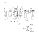
- FIG. 6 shows a plan view of a second embodiment of the wired circuit board of the present invention.
- FIG. 7 is an enlarged cross-sectional view along the line XX of the printed circuit board shown in FIG. 8A to 8F are manufacturing process diagrams of the printed circuit board shown in FIG. 7.
- FIG. 8A is a process for preparing a supporting metal sheet.
- FIG. 8B is a process for placing a metal thin film.
- FIG. 8C is a base insulating layer. 8D shows the step of arranging the wiring layer, FIG.
- FIGS. 10K to 10N are manufacturing process diagrams of the printed circuit board shown in FIG. 7 subsequent to FIG. 8F, in which FIG. 9G is a step of arranging an etching resist, and FIG. 9H is a step of forming a second opening, FIG. 9I shows the step of removing the etching resist, and FIG. 9J prepares the first and second dry film resists, and the first and second photomasks are arranged on the first and second dry film resists. The process which exposes a film resist is shown.
- FIGS. 10K to 10N are manufacturing process diagrams of the printed circuit board shown in FIG.
- FIG. 10K shows the process of forming the first and second etching resists
- FIG. 10L shows the supporting metal sheet.
- An etching process FIG. 10M shows a process of removing the first and second etching resists
- FIG. 10N shows a process of forming a plating film.
- FIG. 11 is a cross-sectional view of the wiring body of the printed circuit board of Comparative Example 2 that does not include the protective metal film.
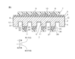
- the printed circuit board 1 has one surface in the thickness direction and the other surface facing each other in the thickness direction, and has a shape extending in the surface direction orthogonal to the thickness direction.
- the printed circuit board 1 includes a supporting metal layer 2, a protective metal film 3, a plating film 4 as an example of a protective thin film, a base insulating layer 5 as an example of an insulating layer, a wiring layer 6, and a cover insulating layer. 7.
- the printed circuit board 1 includes only the supporting metal layer 2, the protective metal film 3, the plating film 4, the base insulating layer 5, the wiring layer 6, and the cover insulating layer 7.
- the supporting metal layer 2 is a heat sink that diffuses heat from the wiring layer 6 to the outside while supporting the printed circuit board 1.
- the supporting metal layer 2 has a substantially comb shape in cross section.
- the supporting metal layer 2 is integrally provided with a base portion 8 and a protruding portion 9.
- the base 8 has a substantially flat plate shape extending in the surface direction.
- the protruding portion 9 extends from the other surface in the thickness direction of the base portion 8 toward the other side in the thickness direction.
- a plurality of projecting portions 9 are arranged in parallel in the first direction (the direction included in the plane direction and corresponding to the parallel direction of the wiring layers 6 described later) at intervals.
- the support metal layer 2 integrally includes a first support surface 10 that is one surface in the thickness direction, a second support surface 11 that is the other surface in the thickness direction, and a support side surface 12 that is a side surface.
- the first support surface 10 is a flat surface along the surface direction.
- the first support surface 10 is one surface in the thickness direction of the base portion 8.
- the second support surface 11 is disposed on the other side in the thickness direction of the first support surface 10 with a gap.
- the second support surface 11 is an uneven surface corresponding to the protruding portion 9.
- the support side surface 12 is a connection surface that connects the peripheral edge of the first support surface 10 and the peripheral edge of the second support surface 11.
- the support side surface 12 is the outer peripheral side surface of the support metal layer 2.
- the support side surface 12 is a flat surface along the thickness direction.
- the first support surface 10, the second support surface 11, and the support side surface 12 form the surface of the support metal layer 2.
- the thermal conductivity of the support metal layer 2 is 5 W / m ⁇ K or more. If the thermal conductivity of the supporting metal layer 2 is less than 5 W / m ⁇ K, the supporting metal layer 2 cannot efficiently release the heat generated in the wiring layer 6 toward the other side in the thickness direction.
- the thermal conductivity of the supporting metal layer 2 is preferably 10 W / m ⁇ K or more, more preferably 15 W / m ⁇ K or more, 20 W / m ⁇ K or more, 25 W / m ⁇ K or more, 30 W / m ⁇ K or more, 35 W / m ⁇ K or more, 40 W / m ⁇ K or more, 50 W / m ⁇ K or more, 60 W / m ⁇ K or more, 75 W / m ⁇ K or more, 100 W / m ⁇ K or more, 200 W / m ⁇ K As described above, 300 W / m ⁇ K or more and 350 W / m ⁇ K or more are preferable.
- the thermal conductivity of the support metal layer 2 is, for example, 10000 W / m ⁇ K or less.
- the thermal conductivity of the metal support layer 6 is determined by JIS H 7903: 2008 (effective thermal conductivity measurement method).
- Examples of the material of the supporting metal layer 2 include metals having excellent thermal conductivity. Further, as the material of the supporting metal layer 2, since the supporting metal layer 2 is protected (rust-proofing) by the protective metal film 3 and the plating film 4 described in detail later, even a metal having low corrosion resistance is allowed. . Specifically, examples of the material for the supporting metal layer 2 include metals such as copper, silver, iron, aluminum, chromium, and alloys thereof. Preferably, the metal containing copper, such as copper and a copper alloy, is mentioned from a viewpoint of obtaining favorable thermal conductivity. In addition, the material of the base 8 and the protrusion 9 is the same.
- the dimensions of the support metal layer 2 are appropriately set according to the use and purpose.
- the thickness of the base 8 is, for example, 30 ⁇ m or more, preferably 100 ⁇ m or more, and for example, 10 mm or less.
- the protruding length (thickness direction length) of the protruding portion 9 from the other surface in the thickness direction of the base portion 8 is, for example, 100 ⁇ m or more and, for example, 100 mm or less.
- the protective metal film 3 is disposed on the entire surface of the support metal layer 2 between the support metal layer 2 and the base insulating layer 5 described below. Specifically, the protective metal film 3 is disposed on the entire first support surface 10 of the support metal layer 2. That is, the protective metal film 3 covers the entire first support surface 10.
- the protective metal film 3 is, for example, a sputtering thin film or a plating thin film, and is preferably a sputtering thin film. A method for forming the protective metal film 3 will be described later.
- Examples of the material for the protective metal film 3 include metals having excellent corrosion resistance. Specifically, examples of the material of the protective metal film 3 include metals such as chromium, nickel, and alloys thereof. Further, the metal may include the above-described metal oxide, and examples thereof include chromium oxide. Preferably, chromium is used.
- the thickness of the protective metal film 3 is, for example, substantially the same length across the surface direction.
- the thickness of the protective metal film 3 is, for example, 1 nm or more, preferably 10 nm or more, more preferably 20 nm or more, still more preferably 100 nm or more, and for example, 10,000 nm or less, preferably 1000 nm or less, more preferably. Is 500 nm or less.
- the plating film 4 is a corrosion resistance-imparting layer (rust prevention layer) that improves the corrosion resistance of the second support surface 11 and the support side surface 12 that are examples of exposed surfaces exposed from the protective metal film 3 in the support metal layer 2. is there.
- the plating film 4 is disposed on the second support surface 11 and the support side surface 12 of the support metal layer 2. Specifically, the plating film 4 continuously contacts and covers the second support surface 11 and the support side surface 12.
- the plating film 4 is formed following the uneven surface of the second support surface 11.
- the entire surface of the support metal layer 2 is protected (covered) by the protective metal film 3 and the plating film 4. That is, the first support surface 10 of the support metal layer 2 is protected by the protective metal film 3, and the second support surface 11 and the support side surface 12 of the support metal layer 2 are protected by the plating film 4.
- the plating film 4 is a layer formed by plating described later.
- the plating film 4 may be either a single layer or multiple layers.
- the plating film 4 includes a first plating film and a second plating film that are sequentially formed on the second support surface 11 and the support side surface 12.
- the material of the plating film 4 examples include corrosion resistant metals (rust preventive metals) such as nickel, gold, and alloys thereof.
- the material of a 1st plating film is nickel and the material of a 2nd plating film is gold
- the thickness of the plating film 4 is not particularly limited, and is, for example, 1 nm or more, preferably 10 nm or more, more preferably 100 nm or more, and for example, 1000 ⁇ m or less, preferably 100 ⁇ m or less.
- the base insulating layer 5 is an insulating layer intended to insulate the wiring layer 6 and the protective metal film 3, and thus insulate the wiring layer 6 and the supporting metal layer 2.
- the base insulating layer 5 is disposed on one surface in the thickness direction of the protective metal film 3. Specifically, the base insulating layer 5 is in contact with the entire one surface in the thickness direction of the protective metal film 3. Further, the insulating base layer 5 is adjacently disposed on one side in the thickness direction of the supporting metal layer 2 with an interval (interval at which the protective metal film 3 is formed).
- the base insulating layer 5 has a sheet shape extending along the surface direction.
- Examples of the material of the base insulating layer 5 include insulating resins such as thermosetting resins and thermoplastic resins.
- the material of the base insulating layer 5 includes a transparent resin having transparency.
- Examples of the thermosetting resin include an epoxy resin and a thermosetting polyimide resin.
- Examples of the thermoplastic resin include an acrylic resin.
- a thermosetting resin is mentioned, More preferably, a thermosetting polyimide resin is mentioned.
- the wiring layer 6 transmits an electrical signal, for example.
- the wiring layer 6 is disposed on one surface in the thickness direction as an example of the surface of the base insulating layer 5.
- the wiring layers 6 are arranged in parallel in the first direction at intervals.
- the wiring layer 6 extends in the second direction (a direction included in the plane direction and is orthogonal to the first direction and the thickness direction; the depth direction in the drawing in FIG. 1). Terminals (not shown) are connected to both ends of the two directions.
- Examples of the material of the wiring layer 6 include copper, silver, gold, iron, aluminum, chromium, and alloys thereof.
- copper is used from the viewpoint of obtaining good electrical characteristics.
- the thickness of the wiring layer 6 is, for example, 1 ⁇ m or more, preferably 5 ⁇ m or more, and for example, 50 ⁇ m or less, preferably 3 ⁇ m or less.
- the width and interval of the wiring layer 6 are, for example, 1 ⁇ m or more, preferably 5 ⁇ m or more, and for example, 200 ⁇ m or less, preferably 100 ⁇ m or less.
- the insulating cover layer 7 is an insulating layer that protects the surface of the wiring layer 6.
- the insulating cover layer 7 is disposed on one surface in the thickness direction of the insulating base layer 5 so as to cover the wiring layer 6. Specifically, the insulating cover layer 7 is in contact with one surface and side surfaces in the thickness direction of the wiring layer 6 and one surface in the thickness direction of the base insulating layer 5 around the wiring layer 6.
- the material of the insulating cover layer 7 is the same as that of the insulating base layer 5.
- the insulating cover layer 7 has a thickness of, for example, 1 ⁇ m or more, preferably 5 ⁇ m or more, and for example, 100 ⁇ m or less, preferably 50 ⁇ m or less.
- the method of manufacturing the printed circuit board 1 includes a step of preparing the supporting metal layer 2 (see FIG. 2A), a step of arranging the protective metal film 3 (see FIG. 2B), and a step of arranging the base insulating layer 5 (see FIG. 2C).
- the above steps are performed in the order described above.
- a thick plate member is prepared, and then the outer shape is processed so that the protruding portion 9 is formed.
- a supporting metal layer 2 comprising 9 is formed.
- a metal thin film forming method such as a dry process or a wet process is used.
- the dry process include sputtering, ion plating, and vacuum deposition.
- the wet process include plating. These can be used alone or in combination.
- a dry process more preferably, sputtering is used.
- the protective metal film 3 is formed on the entire surface of the first support surface 10 of the support metal layer 2 by the metal thin film formation method described above. In addition, also by the metal thin film formation method described above, the protective metal film 3 is not formed on the second support surface 11 and the support side surface 12 of the support metal layer 2 and is still exposed.
- the insulating resin described above is applied to one side in the thickness direction of the protective metal film 3 and dried to form a film. Then, if necessary, it is heated. Further, if the insulating resin is a thermosetting resin, a B-stage film is formed by the above-described application and drying, and then the C-stage is formed by heating.
- a wiring formation method such as an additive method or a subtractive method is used.
- the insulating resin described above is applied and dried on one surface in the thickness direction of the protective metal film 3 to form a film, Then, if necessary, it is heated.
- the plating preparation body 22 including the supporting metal layer 2, the protective metal film 3, the base insulating layer 5, the wiring layer 6, and the cover insulating layer 7 is produced.
- the second support surface 11 and the support side surface 12 of the support metal layer 2 are plated, and the plating film 4 is applied to the second support surface 11 and the support side surface 12.
- plating examples include electrolytic plating and electroless plating. Preferably, electroless plating is used.
- the plating preparation 22 is immersed in a plating bath (plating solution).
- the plating solution contains the above-mentioned corrosion-resistant metal and / or its ions.
- the blending ratio of the above components, plating conditions, and the like are set as appropriate.
- a corrosion-resistant metal grows from the second support surface 11 and the support side surface 12 of the support metal layer 2 to form the plating film 4.
- the printed circuit board 1 does not include the protective metal film 3 (see FIG. 1), and the other surface in the thickness direction of the base insulating layer 5 is the first support surface of the support metal layer 2.
- a minute gap 19 is easily formed between the peripheral edge of the other surface in the thickness direction of the insulating base layer 5 and the peripheral edge of the first support surface 10.
- the plating solution cannot sufficiently enter the gap 19, so that the peripheral edge facing the gap 19 on the first support surface 10.
- the plating film 4 (plating) is not formed on the edge, and remains exposed. Then, the peripheral edge of the first support surface 10 becomes a starting point of corrosion, and as a result, the entire support metal layer 2 is corroded.
- the protective metal film 3 is disposed on the entire first support surface 10 of the support metal layer 2. Therefore, as shown in FIG. 3F, when the plating film 4 is formed by plating, the peripheral edge of the first support surface 10 of the support metal layer 2 is exposed even if the plating solution does not enter the gap 19 described above. As a result, the above-described corrosion can be suppressed.
- the plating film 4 is also disposed on the second support surface 11 and the support side surface 12 of the support metal layer 2.
- the supporting metal layer 2 is excellent in corrosion resistance.
- the use of such a printed circuit board 1 is not particularly limited and is used in various fields.
- the printed circuit board 1 is used in various applications such as a printed circuit board for electronic equipment (wired circuit board for electronic parts) and a wired circuit board for electrical equipment (wired circuit board for electrical parts).
- Examples of the wiring circuit board for electronic equipment and the wiring circuit board for electric equipment include wiring circuit boards for sensors used in sensors such as position information sensors, obstacle detection sensors, and temperature sensors, such as automobiles, trains, airplanes, and machine tools.
- Wiring circuit boards for transportation vehicles used in transportation vehicles such as vehicles, for example, wiring circuit boards for video equipment used in video equipment such as flat panel displays, flexible displays, projection type video equipment, such as network equipment, large communication equipment
- Wiring circuit boards for communication relay equipment used in communication relay equipment such as, for example, wiring circuit boards for information processing terminals used in information processing terminals such as computers, tablets, smartphones, home games, etc., such as drones, robots, etc.
- Mobile equipment distribution used in mobile equipment Circuit boards for example, medical equipment wiring circuit boards used in medical equipment such as wearable medical devices and medical diagnostic equipment, for example, electrical equipment used in electric equipment such as refrigerators, washing machines, vacuum cleaners, and air conditioners
- Wiring circuit boards for recording for example, wiring circuit boards for recording electronic equipment used in recording electronic equipment such as digital cameras and DVD recording devices.
- the plating film 4 is cited as an example of the protective thin film of the present invention, for example, a resin protective thin film made of an organic material may be used.
- organic materials include polymers (resins) such as epoxy polymers, acrylic polymers, and urethane polymers.
- the support metal layer 2 has the protruding portion 9, but, for example, although not shown, the supporting metal layer 2 may not be provided with the protruding portion 9 and may be formed only from the base portion 8.
- the support metal layer 2 has a substantially rectangular cross section, and the second support surface is a flat surface parallel to the first support surface 10.
- the plating film 4 that is an example of the protective thin film is formed by plating.
- the protective thin film specifically, the resin protective thin film
- the protective thin film is formed by a wet process other than plating. can do.
- the protective thin film is a plating film 4. If the protective thin film is a plating film, the hard plating film 4 can reliably adhere the exposed surface of the supporting metal layer 2. Therefore, the plating film 4 can improve the corrosion resistance of the support metal layer 2.
- the protective thin film as long as the exposed surface of the support metal layer 2 (second support surface 11 and support side surface 12) can be protected, from the viewpoint of action, it is not limited to the corrosion resistance imparting layer (rust prevention layer).
- a coating agent rust preventive coating agent
- an abrasion resistant layer a chemical resistant layer
- a weather resistant layer a marking imparting layer
- an antistatic layer may be used.
- the insulating layer (base insulating layer 5) is disposed only on one side in the thickness direction of the supporting metal layer 2, but at least one side in the thickness direction of the supporting metal layer 2.
- an insulating layer (a base insulating layer 5 and a second base insulating layer to be described next) is formed on both sides of the supporting metal layer 2 in the thickness direction on one side and the other side. 36) may be arranged.
- the printed circuit board 1 in which the insulating layers are arranged on both sides in the thickness direction of the supporting metal layer 2 includes, in addition to the above-described layers, a second protective metal film 35, A two-base insulating layer 36, a second wiring layer 37, and a second cover insulating layer 38 are provided.
- the second protective metal film 35 is disposed on the entire surface of the second support surface 11 of the protruding portion 9 that faces the wiring layer 6 in the thickness direction among the second support surface 11 of the support metal layer 2. Note that the plating film 4 is not formed on the entire surface of the second support surface 11 of the protruding portion 9 facing the wiring layer 6 in the thickness direction, and the second protective metal film 35 is formed.
- the material, dimensions, and the like of the second protective metal film 35 are the same as those of the protective metal film 3.
- the entire surface of the support metal layer 2 is protected (covered) by the second protective metal film 35, the protective metal film 3, and the plating film 4.
- the second insulating base layer 36 is disposed on the other surface in the thickness direction of the second protective metal film 35.
- the second insulating base layer 36 is disposed on the other side in the thickness direction of the supporting metal layer 2 via the second protective metal film 35.
- the second protective metal film 35 is disposed on the entire surface of the second support surface 11 of the protrusion 9 between the protrusion 9 and the second base insulating layer 36.
- the length (width) in the first direction of the second base insulating layer 36 is the same as that of the protrusion 9.
- the material, thickness, and the like of the second base insulating layer 36 are the same as those of the base insulating layer 5.
- the second wiring layer 37 is disposed on the other surface in the thickness direction as an example of the surface of the second base insulating layer 36.
- the length (width) in the first direction of the second wiring layer 37 is appropriately selected from the range exemplified for the wiring layer 6.
- the material, thickness, etc. of the second wiring layer 37 are the same as those of the wiring layer 6.
- the second cover insulating layer 38 is disposed on the other surface in the thickness direction of the second base insulating layer 36 so as to cover the second wiring layer 37.
- the material and thickness of the second insulating cover layer 38 are the same as those of the insulating cover layer 7.
- the supporting metal layer 2 is prepared, and then the protective metal film 3 and the second protective metal film 35 are arranged, and then the base insulating layer 5 and the second insulating metal film 2 are arranged.
- the base insulating layer 36 is arranged, then the wiring layer 6 and the second wiring layer 37 are arranged, then the cover insulating layer 7 and the second cover insulating layer 38 are arranged, and then the plating film 4 is arranged.
- the second protective metal film 35 for example, first, the support side surface 12 and the second support surface 11 on which the second protective metal film 35 is not formed are masked, and then the second support surface 11 exposed from the mask. Then, a second protective metal film 35 is formed. Thereafter, the mask is removed.
- the second protective metal film 35 can be formed simultaneously with the protective metal film 3.
- the second protective metal film 35 is disposed on the entire surface of the second support surface 11 in the protruding portion 9 of the support metal layer 2. Therefore, when the plating film 4 is formed by plating, it is possible to prevent the peripheral edge of the second support surface 11 of the protruding portion 9 from being exposed even if the plating solution does not enter the above-described gap. The above corrosion can be suppressed.
- the plating film 4 is also disposed on the support side surface 12 of the support metal layer 2 and the second support surface 11 exposed from the second protective metal film 35.
- the supporting metal layer 2 is excellent in corrosion resistance.
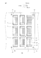
- a plurality of wired circuit boards 1 are provided on the wired circuit board assembly sheet 20.
- the printed circuit board assembly sheet 20 has one surface in the thickness direction and the other surface, and has a substantially rectangular sheet shape extending in a surface direction (direction including the first direction and the second direction) orthogonal to the thickness direction.
- the wired circuit board aggregate sheet 20 is an aggregate sheet including a plurality of wired circuit boards 1 and a plurality of alignment marks 21. As shown in FIG. 7, the printed circuit board assembly sheet 20 includes the above-described support metal layer 2, protective metal film 3, plating film 4, base insulating layer 5, wiring layer 6, and cover insulating layer 7.
- a plurality of wired circuit boards 1 are arranged and arranged at intervals in the wired circuit board assembly sheet 20.
- the printed circuit board 1 is connected to the printed circuit board assembly sheet 20 around the printed circuit board 1 by a joint (not shown) in the printed circuit board assembly sheet 20.
- the printed circuit board 1 has a shape that extends long in the second direction.
- the printed circuit board 1 is integrally provided with two connecting bodies 23 and a wiring body 24 that are spaced apart in the second direction.
- the connecting body 23 forms both ends of the printed circuit board 1 in the second direction.
- the connecting body 23 has a substantially rectangular flat plate shape in plan view that is slightly longer in the first direction.
- the connecting body 23 includes a terminal portion 34.
- the terminal portions 34 are arranged in parallel at intervals in the first direction.
- Each terminal portion 34 has a substantially rectangular (land) shape in plan view.
- the wiring body 24 forms the intermediate portion in the second direction of the printed circuit board 1.
- the wiring body 24 is disposed between the two connecting bodies 23 in plan view.
- the wiring body 24 has a shape extending in the second direction.
- the wiring body 24 bridges the two connecting bodies 23 in the second direction.
- a plurality of wiring bodies 24 are arranged in parallel at intervals in the first direction. Each of the ends in the second direction of the plurality of wiring bodies 24 is connected in the second direction by the two first connecting bodies 2.
- an opening 25 is formed between adjacent wiring bodies 24.
- a plurality of openings 25 are formed in parallel in the first direction with the wiring body 24 therebetween.
- Each of the plurality of openings 25 has a shape extending in the second direction and penetrates the printed circuit board 1 in the thickness direction.
- the wiring bodies 24 and the openings 25 are alternately arranged in the second direction.
- the length (width) in the first direction of each of the plurality of wiring bodies 24 is, for example, 500 ⁇ m or less, preferably 300 ⁇ m or less, more preferably 100 ⁇ m or less, and for example, 10 ⁇ m or more.
- the first direction length (width) of each of the plurality of openings 25 is, for example, 10 ⁇ m or more, preferably 50 ⁇ m or more, more preferably 100 ⁇ m or more, and for example, 1000 ⁇ m or less.
- the ratio of the length in the first direction of the wiring body 24 to the length in the first direction of the opening 25 is, for example, 40 or less, preferably 10 or less, and for example, 0.1 or more, preferably 0. .5 or more.
- Alignment marks 21 are arranged at each of the four corners.
- Each of the plurality of alignment marks 21 has a substantially circular shape in plan view.
- connection body 23 is demonstrated easily.
- Each of the plurality of wiring bodies 24 includes a supporting metal layer 2, a protective metal film 3, a plating film 4, a base insulating layer 5, a wiring layer 6, and a cover insulating layer 7 independently of each other.
- the support metal layer 2 is a heat sink that diffuses heat from the wiring layer 6 to the outside while supporting the wiring body 24.
- the supporting metal layer 2 has a substantially rectangular shape in sectional view.
- the support metal layer 2 integrally includes a first support surface 10, a second support surface 11, and a support side surface 12.
- the second support surface 11 is a flat surface parallel to the first support surface 10.
- the first support surface 10, the second support surface 11, and the support side surface 12 in the wiring body 24 form the surface of the support metal layer 2 in the wiring body 24.
- the thickness of the support metal layer 2 in the wiring body 24 is formed by etching the support metal sheet 42 described later from both sides in the thickness direction, it is allowed to be relatively thick.
- the thickness of the supporting metal layer 2 is, for example, 50 ⁇ m or more, preferably 100 ⁇ m or more, preferably 250 ⁇ m or more, preferably 500 ⁇ m or more, preferably 1000 ⁇ m or more, and for example, 10 mm or less.
- the ratio of the thickness of the supporting metal layer 2 to the width is, for example, 2 or more, preferably 2.5 or more, more preferably 3 or more, still more preferably 3.5 or more, For example, it is 1000 or less.
- the length (width) in the first direction of the support metal layer 2 is appropriately selected from the range exemplified by the length in the first direction of the wiring body 24 described above, and specifically, the same as the length in the first direction of the wiring body 24. It is.
- the protective metal film 3 is disposed on the entire surface of the support metal layer 2 between the support metal layer 2 and the base insulating layer 5. Specifically, the protective metal film 3 is disposed on the entire first support surface 10 of the support metal layer 2 in the wiring body 24. That is, the protective metal film 3 covers the entire first support surface 10 of the support metal layer 2.
- the plating film 4 is a corrosion resistance imparting layer (rust prevention layer) that improves the corrosion resistance of the second support surface 11 and the support side surface 12 of the support metal layer 2.
- the plating film 4 is disposed on a second support surface 11 and a support side surface 12 as an example of an exposed surface exposed from the support metal layer 2.
- the plating film 4 has a substantially U-shaped cross section that opens toward one side in the thickness direction in the wiring body 24.
- the entire surface of the support metal layer 2 in the wiring body 24 is protected (covered) by the protective metal film 3 and the plating film 4. That is, the first support surface 10 of the support metal layer 2 in the wiring body 24 is protected by the protective metal film 3, and the second support surface 11 and the support side surface 12 of the support metal layer 2 in the wiring body 24 are protected by the plating film 4. Protected.
- the base insulating layer 5 is an insulating layer for insulation between the wiring layer 6 and the protective metal film 3, and consequently insulation between the wiring layer 6 and the supporting metal layer 2.
- the base insulating layer 5 is disposed on one surface in the thickness direction of the protective metal film 3.
- the wiring layer 6 is disposed on one surface in the thickness direction as an example of the surface of the base insulating layer 5.
- one wiring layer 6 is provided in one wiring body 24. Both ends of the wiring layer 6 in the second direction are continuous with the terminal portion 34 (see FIG. 6).
- the insulating cover layer 7 is an insulating layer that protects one side surface and the side surface in the thickness direction of the wiring layer 6.
- the insulating cover layer 7 is in contact with one surface and side surfaces in the thickness direction of the wiring layer 6 and one surface in the thickness direction of the base insulating layer 5 around the wiring layer 6.
- connection body 23 is provided with the member corresponding to each above-mentioned layer (except the wiring layer 6) and each film
- the connecting body 23 includes a terminal portion 34 formed from the same layer as the wiring layer 6.
- the alignment mark 21 is formed of an alignment mark metal film 31 exposed from the support metal layer 2.
- the second opening 41 is formed in the support metal layer 2 on which the alignment mark metal film 31 is disposed.
- the second opening 41 is a through-hole in the thickness direction of the support metal layer 2 and has a size larger than the alignment mark opening 33 so as to include an alignment mark opening 33 (described later) in a bottom view.
- the maximum length in the surface direction of the second opening 41 is, for example, 0.02 mm or more, preferably 0.2 mm or more, more preferably For example, it is 50 mm or less, preferably 25 mm or less.
- Alignment mark metal film 31 has an alignment mark opening 33 at the center.
- the outer shape (outer edge) shape of the alignment mark metal film 31 is not particularly limited as long as it has the alignment mark opening 33 described above.
- the alignment mark metal film 31 includes the flange portion 13 exposed from the second opening 41 in the bottom view because the alignment mark opening 33 is included in the second opening 41 in the bottom view.
- the alignment mark metal film 31 is formed in the shape described above from the same metal thin film 43 (see FIG. 8A described later) together with the protective metal film 3 in the wiring body 24.
- the alignment mark metal film 31 integrally connects the portion of the support metal layer 2 disposed on the first support surface 10 and the flange portion 13 that is not supported by the first support surface 10 and is exposed from the second opening 41. Prepare.
- an inner edge (inner peripheral end surface) 40 facing the alignment mark opening 33 constitutes the alignment mark 21.
- the shape of the inner edge 40 is not particularly limited, and examples thereof include a substantially circular shape in plan view (or bottom view).
- the inner end edge 40 of the alignment mark metal film 31 is exposed (surface) toward the other side in the thickness direction through the second opening 41.
- the maximum length in the surface direction of the alignment mark opening 33 (in the case of a substantially circular shape in a plan view) is, for example, 0.01 mm or more, preferably 0.1 mm or more, more preferably 1 mm or more, For example, it is 25 mm or less, preferably 10 mm or less.
- the maximum length of the alignment mark opening 33 is smaller than the maximum length in the surface direction of the second opening 41, and the maximum length of the alignment mark opening 33 is relative to the maximum length of the second opening 41.
- the ratio is, for example, less than 1, preferably 0.9 or less, more preferably 0.8 or less, and even more preferably 0.7 or less. For example, the ratio is 0.1 or more, preferably 0. 2 or more.
- the plating film 4 is also disposed on the inner peripheral surface facing the second opening 41.
- the base insulating layer 5 having the insulating opening 50 having the same shape as that of the alignment mark opening 33 in plan view is formed on one surface in the thickness direction of the alignment mark metal film 31.
- any of a single wafer type (batch type) (refer the continuous line of FIG. 6) and a roll-to-roll type (refer to the virtual line of FIG. 6) can be implemented.
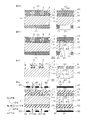
- the method for manufacturing the printed circuit board 1 includes a step of preparing the supporting metal sheet 42 (see FIG. 8A), a step of arranging the metal thin film 43 (see FIG. 8B), and a step of arranging the base insulating layer 5 (see FIG. 8C).
- the method of manufacturing the printed circuit board 1 includes the step of forming the second opening 41 in the support metal sheet 42 (see FIGS. 9G to 9I), the first etching resist 45 and the second etching resist as an example of the etching resist.
- a step of disposing the etching resist 55 is provided.
- the method of manufacturing the printed circuit board 1 includes a step of etching the supporting metal sheet 42 from one side and the other side in the thickness direction (see FIGS. 10L to 10M), a step of forming the plating film 4 (see FIG. 10N), and And a step of taking out the printed circuit board 1 from the printed circuit board assembly sheet 20.
- a substantially sheet (plate) -shaped support metal sheet 42 extending in the surface direction is prepared.
- the support metal sheet 42 is a support metal preparation sheet for forming the support metal layer 2 of the wiring body 24 and the second opening 41 of the alignment mark 21.
- the supporting metal sheet 42 is an etching sheet for forming the second opening 41 by etching.
- the support metal sheet 42 has a first support surface 10 and a second support surface 11.
- the thermal conductivity and material of the support metal sheet 42 are the same as those of the support metal layer 2 described above.
- the metal thin film 43 is formed on the entire first support surface 10 of the support metal sheet 42 by the above-described metal thin film forming method (preferably sputtering). .
- the metal thin film 43 is a preparation thin film for forming the protective metal film 3 and the alignment mark metal film 31.
- the base insulating layer 5 is formed on one surface in the thickness direction of the metal thin film 43 with the above-described pattern.
- a photosensitive resin is applied to one surface in the thickness direction of the protective metal film 3, and the base insulating layer 5 corresponding to the wiring body 24 is formed by photolithography that exposes and develops.
- An insulating opening 50 is formed in the base insulating layer 5.
- the wiring layer 6 is formed on one surface in the thickness direction of the base insulating layer 5.
- the metal thin film 43 exposed from the base insulating layer 5 is removed.
- the metal thin film 43 around the base insulating layer 5 of the wiring body 24 and the metal thin film 43 exposed from the insulating opening 50 are simultaneously removed.
- etching, peeling, or the like using the base insulating layer 5 as a mask (resist) is used.
- the protective metal film 3 corresponding to the wiring body 24 and the alignment mark metal film 31 having the alignment mark opening 33 are simultaneously formed from the same metal thin film 43.
- the cover insulating layer 7 is formed so as to cover the wiring layer 6 on one surface in the thickness direction of the base insulating layer 5.
- etching is used in the step of forming the second opening 41 in the support metal layer 2.
- an etching resist 44 is applied to the first support surface 10 of the support metal sheet 42, the side surface of the protective metal film 3, and the base insulating layer. 5 is continuously arranged in the entire surface direction so as to cover the side surface of the cover 5 and the side surface of the insulating cover layer 7 and one surface in the thickness direction.
- the etching resist 44 is arranged on the second supporting surface 11 of the supporting metal sheet 42 so that an etching resist opening 51 having the same pattern as the second opening 41 to be formed next is formed in the bottom view. .
- the supporting metal sheet 42 exposed from the etching resist 44 is etched. Specifically, the supporting metal sheet 42 exposed from the etching resist opening 51 is removed by etching from the other side in the thickness direction.
- the second opening 41 is formed in the support metal sheet 42.
- the inner edge 40 of the alignment mark opening 33 is exposed toward the other side in the thickness direction. Therefore, the inner edge 40 becomes the alignment mark 21 that is visually recognized from the other side in the thickness direction through the second opening 41. On the other hand, since the base insulating layer 5 has transparency, the inner edge 40 is also visually recognized from one side in the thickness direction.
- a wiring circuit sheet 60 including the supporting metal sheet 42, the base insulating layer 5, the wiring layer 6, the cover insulating layer 7, the protective metal film 3, and the alignment mark metal film 31 is obtained.
- the wiring circuit sheet 60 does not yet include the wiring body 24, the plating film 4, and the opening 25.
- the wiring circuit sheet 60 is a preparation sheet for manufacturing the wiring circuit board assembly sheet 20.
- the first etching resist 45 and the second etching resist 45 are arranged using the inner edge 40 of the alignment mark metal film 31 as a positioning reference.
- Each of the etching resists 55 is arranged on the one side and the other side in the thickness direction of the support metal sheet 42 so as to have substantially the same pattern as the support metal layer 2 to be formed next when projected in the thickness direction.
- each of the first dry film resist 49 and the second dry film resist 59 is disposed on the entire one surface and the other surface of the supporting metal sheet 42 in the thickness direction.
- Examples of the first dry film resist 49 and the second dry film resist 59 include a negative photoresist (negative photoresist).
- Each of the first dry film resist 49 and the second dry film resist 59 is continuously formed in the surface direction.
- both the first dry film resist 49 and the second dry film resist 59 have translucency (transparency) to such an extent that the inner edge 40 can be viewed from both sides in the thickness direction.
- the first dry film resist 49 is disposed on the first support surface 10 so as to fill the insulating opening 50 and the alignment mark opening 33 but close one edge of the second opening 41 in the thickness direction. Further, the first dry film resist 49 is covered with the first side of the protective metal film 3, the side of the base insulating layer 5, and the one side and side of the cover insulating layer 7 in the thickness direction. 1 Arranged on the support surface 10.
- the second dry film resist 59 is disposed on the second support surface 11 so as to close the other end of the second opening 41 in the thickness direction.
- the first photomask 46 having the first light transmitting portion 47 and the first light shielding portion 48 is disposed on one side in the thickness direction of the first dry film resist 49.
- the first light-transmitting portion 47 is a portion that transmits light when the first dry film resist 49 is exposed, and is a first etching resist opening 52 (and further formed next in the first etching resist 45). , And has a pattern corresponding to the opening 25) shown in FIG. 10L.
- the first light shielding portion 48 is a portion that shields light when the first dry film resist 49 is exposed, and has a pattern corresponding to the opening 25.
- the second photomask 56 having the second light transmitting portion 57 and the second light shielding portion 58 is disposed on the other side in the thickness direction of the second dry film resist 59.
- the second light transmitting portion 57 is a portion that transmits light when the second dry film resist 59 is exposed, and has the same pattern as the first light transmitting portion 47.
- the second light shielding portion 58 is a portion that shields light when the second dry film resist 59 is exposed, and has the same pattern as the first light shielding portion 48.
- the first photomask 46 and A second photomask 56 is disposed.
- the first light transmitting portion 47 and the second light transmitting portion 57 are positioned in the plane direction so as to overlap (match) each other when projected in the thickness direction using the inner edge 40 as a positioning reference. To do. At the same time, when projected in the thickness direction using the inner edge 40 as a positioning reference, the first light-shielding portion 48 and the second light-shielding portion 58 are positioned in the surface direction so as to overlap (match) each other.
- the inner edge 40 is observed by a camera (illustrated) from one side in the thickness direction through the insulating base layer 5 and the first dry film resist 49.
- the inner edge 40 is observed by the camera from the other side in the thickness direction through the second dry film resist 59 and the second opening 41.
- the first dry film resist 49 is exposed through the first photomask 46.
- the second dry film resist 59 is exposed through the second photomask 56.
- the second dry film resist 59 is formed with a photosensitive portion that is exposed to light transmitted through the second light transmitting portion 57 and an unexposed portion corresponding to the second light shielding portion 58.
- the first dry film resist 49 and the second dry film resist 59 are heated after exposure.
- the first dry film resist 49 and the second dry film resist 59 are developed.
- the unexposed portion is removed and the exposed portion remains.
- the first etching resist 45 having the first etching resist opening 52 is formed from the first dry film resist 49.
- a second etching resist 55 having a second etching resist opening 53 is formed from the second dry film resist 59.
- the first etching resist 45 and the second etching resist 55 have substantially the same pattern as the supporting metal layer 2.
- the supporting metal sheet 42 corresponding to the first etching resist opening 52 is formed with a thickness.
- the supporting metal sheet 42 corresponding to the second etching resist opening 53 is etched from the other side in the thickness direction.
- the supporting side surface 12 of the supporting metal layer 2 constituting the wiring body 24 is allowed to recede further in the first direction due to over-etching in which etching proceeds excessively.
- the supporting metal layer 2 of the wiring body 24 is formed from the supporting metal sheet 42.
- the first etching resist 45 and the second etching resist 55 are removed. Thereby, the plating preparation body 22 before forming the plating film 4 is produced.
- the second support surface 11 and the support side surface 12 of the support metal layer 2 are plated.
- the alignment mark 21 including the printed circuit board 1 and the alignment mark 21 is obtained.
- the joint (not shown) is cut, the printed circuit board 1 is separated from the surroundings, and taken out from the printed circuit board assembly sheet 20. Thus, the printed circuit board 1 is manufactured.
- the wiring body 24 does not include the protective metal film 3 (see FIG. 7), and the other surface in the thickness direction of the base insulating layer 5 is the first support surface 10 of the support metal layer 2.
- the peripheral edge of the other surface in the thickness direction of the base insulating layer 5 is excessively removed (over-development) during development in photolithography processing (exposure and development) when forming the base insulating layer 5.
- a minute gap 19 is easily formed between the peripheral edge of the other surface in the thickness direction of the insulating base layer 5 and the peripheral edge of the first support surface 10. Then, in the plating on the support side surface 12 of the support metal layer 2 as shown in FIG.
- the plating solution cannot sufficiently enter the gap 19, so that the peripheral edge facing the gap 19 on the first support surface 10.
- the plating film 4 is not formed on the edge and remains exposed. Then, the peripheral edge of the first support surface 10 becomes a starting point of corrosion, and consequently, the support metal layer 2 in each of the plurality of wiring bodies 24 is corroded.
- the protective metal film 3 is disposed on the entire surface of the first support surface 10 of the support metal layer 2 in each of the plurality of wiring bodies 24. . Therefore, corrosion of the peripheral edge of the first support surface 10 of the support metal layer 2 due to the formation of the gap 19 (see FIG. 11) can be suppressed. Further, the plating film 4 is disposed on the second support surface 11 and the support side surface 12 of the support metal layer 2.
- the supporting metal layer 2 in the wiring body 24 is excellent in corrosion resistance.
- the second etching resist 55 having the etching resist opening 53 is projected on the first support surface 10 and the second support surface 11 of the support metal sheet 42 in the thickness direction, it has substantially the same pattern as the support metal layer 2.
- the positional accuracy of the first etching resist opening 52 and the second etching resist opening 53 is high. Therefore, the supporting metal sheet 42 exposed from the first etching resist opening 52 and the second etching resist opening 53 is etched from one side and the other side in the thickness direction so that the supporting metal layer 2 is highly accurate in a short time. Can be formed.
- the wiring circuit sheet 60 includes the alignment mark metal film 31 having the alignment mark opening 33, so that the inner edge 40 of the alignment mark metal film 31 is connected to the one side in the thickness direction and the other side.
- the positioning reference can be confirmed from both sides.
- the first photomask 46 and the second photomask 56 are arranged with the inner edge 40 as a positioning reference, and the first etching resist is exposed and developed.
- the opening 52 and the second etching resist opening 53 can be formed.
- the use of the printed circuit board 1 is not particularly limited, and is used in various fields.
- the printed circuit board 1 is used in various applications such as a printed circuit board for electronic equipment (wired circuit board for electronic parts) and a wired circuit board for electrical equipment (wired circuit board for electrical parts).
- the printed circuit board assembly sheet 20 includes a plurality of alignment marks 21 (specifically, four), but the number is not particularly limited.
- the printed circuit board assembly sheet 20 includes the alignment mark 21, it is sufficient that the printed wiring circuit sheet 60 includes the alignment mark 21 (inner edge 40). After the board 1 is provided on the printed circuit board assembly sheet 20, the alignment mark 21 can be removed. That is, in this case, the printed circuit board assembly sheet 20 does not include the alignment mark 21.
- the second opening 41 is formed by etching (wet process).
- etching wet process
- laser processing dry process
- water jet The second opening 41 can also be formed by (water cutter) or press punching.
- etching is used. In the case of etching, the second opening 41 is formed, but the alignment mark metal film 31 can be reliably left.
- a negative photoresist (negative photoresist) is used as the first dry film resist 49 and the second dry film resist 59.
- a positive photoresist (positive photoresist) is used. It can also be used.
- the first dry film resist 49 and the second dry film resist 59 are formed from the first etching resist 45 and the second etching resist 55 by photolithography, but, for example, the first etching resist opening 52 is formed in advance.
- one wiring layer 6 is provided in one wiring body 24, a plurality of wiring layers 6 can be provided in one wiring body 24, for example, although not shown.
- the plating film 4 which is an example of the protective thin film is formed by plating.
- the protective thin film specifically, the resin protective thin film
- the protective thin film is formed by a wet process other than plating. be able to.
- the printed circuit board assembly sheet 20 (see FIGS. 7 and 10N) and / or the wired circuit sheet 60 (see FIG. 9I) is disposed on the other side in the thickness direction of the support metal layer 2.
- the protective metal film 35, the second base insulating layer 36, the second wiring layer 37, and the second cover insulating layer 38 can be further provided. In this case, the entire surface of the support metal layer 2 in the wiring body 24 is protected (covered) by the second protective metal film 35, the protective metal film 3, and the plating film 4.
- the wiring circuit board is used in a wiring circuit board for electronic equipment, a wiring circuit board for electric equipment, and the like.
Landscapes
- Engineering & Computer Science (AREA)
- Microelectronics & Electronic Packaging (AREA)
- Manufacturing & Machinery (AREA)
- Condensed Matter Physics & Semiconductors (AREA)
- Materials Engineering (AREA)
- Physics & Mathematics (AREA)
- Chemical & Material Sciences (AREA)
- General Physics & Mathematics (AREA)
- Computer Hardware Design (AREA)
- Power Engineering (AREA)
- Structure Of Printed Boards (AREA)
- Insulated Metal Substrates For Printed Circuits (AREA)
- Cooling Or The Like Of Semiconductors Or Solid State Devices (AREA)
- Manufacturing Of Printed Wiring (AREA)
Priority Applications (3)
| Application Number | Priority Date | Filing Date | Title |
|---|---|---|---|
| CN201980036285.5A CN112205087A (zh) | 2018-05-31 | 2019-05-10 | 布线电路基板及其制造方法和布线电路片材 |
| KR1020207034009A KR102793969B1 (ko) | 2018-05-31 | 2019-05-10 | 배선 회로 기판, 그 제조 방법 및 배선 회로 시트 |
| US17/057,912 US11284503B2 (en) | 2018-05-31 | 2019-05-10 | Wiring circuit board, producing method thereof, and wiring circuit sheet |
Applications Claiming Priority (2)
| Application Number | Priority Date | Filing Date | Title |
|---|---|---|---|
| JP2018104707A JP7066528B2 (ja) | 2018-05-31 | 2018-05-31 | 配線回路基板、その製造方法および配線回路シート |
| JP2018-104707 | 2018-05-31 |
Publications (1)
| Publication Number | Publication Date |
|---|---|
| WO2019230335A1 true WO2019230335A1 (ja) | 2019-12-05 |
Family
ID=68696655
Family Applications (1)
| Application Number | Title | Priority Date | Filing Date |
|---|---|---|---|
| PCT/JP2019/018714 Ceased WO2019230335A1 (ja) | 2018-05-31 | 2019-05-10 | 配線回路基板、その製造方法および配線回路シート |
Country Status (6)
| Country | Link |
|---|---|
| US (1) | US11284503B2 (enExample) |
| JP (1) | JP7066528B2 (enExample) |
| KR (1) | KR102793969B1 (enExample) |
| CN (1) | CN112205087A (enExample) |
| TW (1) | TWI822782B (enExample) |
| WO (1) | WO2019230335A1 (enExample) |
Cited By (1)
| Publication number | Priority date | Publication date | Assignee | Title |
|---|---|---|---|---|
| US20230080659A1 (en) * | 2021-09-15 | 2023-03-16 | Amulaire Thermal Technology, Inc. | Radiator structure |
Families Citing this family (14)
| Publication number | Priority date | Publication date | Assignee | Title |
|---|---|---|---|---|
| JP7211930B2 (ja) * | 2019-12-17 | 2023-01-24 | 日東電工株式会社 | 配線回路基板の製造方法 |
| TWI838562B (zh) * | 2020-07-17 | 2024-04-11 | 梁晉睿 | 複合材料製造方法及其應用 |
| JP7515339B2 (ja) | 2020-08-07 | 2024-07-12 | 日東電工株式会社 | 配線回路基板の製造方法、および配線回路基板 |
| JP7289602B2 (ja) * | 2020-11-13 | 2023-06-12 | 日東電工株式会社 | 配線回路基板、および配線回路基板の製造方法 |
| JP7651335B2 (ja) | 2021-03-23 | 2025-03-26 | 日東電工株式会社 | 配線回路基板の製造方法 |
| JP7714369B2 (ja) * | 2021-04-26 | 2025-07-29 | 日東電工株式会社 | 集合体シート、および、集合体シートの製造方法 |
| JP7715531B2 (ja) * | 2021-04-26 | 2025-07-30 | 日東電工株式会社 | 集合体シート、および、集合体シートの製造方法 |
| TWI786710B (zh) * | 2021-07-07 | 2022-12-11 | 艾姆勒科技股份有限公司 | 散熱器結構 |
| JP7448828B2 (ja) * | 2021-09-30 | 2024-03-13 | 日亜化学工業株式会社 | 配線基板、発光装置及びそれらの製造方法 |
| JP2023066606A (ja) | 2021-10-29 | 2023-05-16 | 日東電工株式会社 | 配線回路基板およびその製造方法 |
| JP2023071122A (ja) * | 2021-11-10 | 2023-05-22 | 日東電工株式会社 | 配線回路基板 |
| US12464642B2 (en) | 2022-06-15 | 2025-11-04 | Nitto Denko Corporation | Wiring circuit board and method of producing the wiring circuit board |
| KR20240062530A (ko) * | 2022-11-02 | 2024-05-09 | 엘지이노텍 주식회사 | 열전모듈 |
| CN119545653A (zh) * | 2024-10-17 | 2025-02-28 | 盐城维信电子有限公司 | 可传输力信号的薄型多层线路板及其制作方法 |
Citations (5)
| Publication number | Priority date | Publication date | Assignee | Title |
|---|---|---|---|---|
| JPH06125155A (ja) * | 1992-10-12 | 1994-05-06 | Denki Kagaku Kogyo Kk | 金属ベース回路基板 |
| JP2003152335A (ja) * | 2001-11-15 | 2003-05-23 | Ngk Spark Plug Co Ltd | 配線基板の製造方法及び配線基板 |
| JP2004214583A (ja) * | 2003-01-09 | 2004-07-29 | Ibiden Co Ltd | 配線板およびその製造方法 |
| JP2007035868A (ja) * | 2005-07-26 | 2007-02-08 | Nitto Denko Corp | 配線回路基板の製造方法 |
| JP2014191845A (ja) * | 2013-03-27 | 2014-10-06 | Dainippon Printing Co Ltd | サスペンション用基板 |
Family Cites Families (20)
| Publication number | Priority date | Publication date | Assignee | Title |
|---|---|---|---|---|
| JPS55140255A (en) | 1979-04-18 | 1980-11-01 | Nec Corp | Heat sink structure |
| JPH08125295A (ja) * | 1994-10-20 | 1996-05-17 | Mitsui Toatsu Chem Inc | 金属ベース回路基板 |
| WO2004066697A1 (ja) * | 2003-01-20 | 2004-08-05 | Fujikura Ltd. | 多層配線板およびその製造方法 |
| WO2004073370A1 (ja) * | 2003-02-13 | 2004-08-26 | Fujikura Ltd. | 多層基板およびその製造方法 |
| KR100688858B1 (ko) * | 2004-12-30 | 2007-03-02 | 삼성전기주식회사 | 스파이럴 3차원 인덕터를 내장한 인쇄회로기판 및 그 제조방법 |
| JP5587116B2 (ja) * | 2009-09-30 | 2014-09-10 | 京セラ株式会社 | 配線基板及び実装構造体 |
| US8513535B2 (en) * | 2009-10-30 | 2013-08-20 | Kyocera Corporation | Circuit board and structure using the same |
| JP2011151367A (ja) * | 2009-12-25 | 2011-08-04 | Sony Corp | 回路基板積層モジュール及び電子機器 |
| US9113569B2 (en) * | 2011-03-25 | 2015-08-18 | Ibiden Co., Ltd. | Wiring board and method for manufacturing same |
| KR101255953B1 (ko) * | 2011-09-27 | 2013-04-23 | 삼성전기주식회사 | 적층형 공진 코일의 제조 방법 |
| US9287034B2 (en) * | 2012-02-27 | 2016-03-15 | Ibiden Co., Ltd. | Printed wiring board, inductor component, and method for manufacturing inductor component |
| JP2014007339A (ja) * | 2012-06-26 | 2014-01-16 | Ibiden Co Ltd | インダクタ部品、その製造方法及びプリント配線板 |
| JP2014032978A (ja) * | 2012-07-31 | 2014-02-20 | Ibiden Co Ltd | インダクタ部品、インダクタ部品の製造方法及び配線板 |
| JP6170790B2 (ja) * | 2013-09-13 | 2017-07-26 | 新光電気工業株式会社 | 配線基板及びその製造方法 |
| US20150116950A1 (en) * | 2013-10-29 | 2015-04-30 | Samsung Electro-Mechanics Co., Ltd. | Coil component, manufacturing method thereof, coil component-embedded substrate, and voltage adjustment module having the same |
| CN105683266B (zh) * | 2013-11-01 | 2020-04-03 | 株式会社可乐丽 | 热塑性液晶聚合物薄膜的制造方法、以及电路基板及其制造方法 |
| KR101642643B1 (ko) * | 2015-01-27 | 2016-07-29 | 삼성전기주식회사 | 코일 부품 및 이의 제조 방법 |
| KR101717970B1 (ko) * | 2015-04-28 | 2017-03-21 | 민동훈 | 다층 구조의 보이스 코일판 및 이를 포함하는 평판형 스피커 |
| JP6788268B2 (ja) * | 2016-02-22 | 2020-11-25 | 株式会社ダイワ工業 | 配線基板又は配線基板材料の製造方法 |
| WO2019188287A1 (ja) * | 2018-03-28 | 2019-10-03 | 株式会社村田製作所 | 樹脂多層基板、アクチュエータ、および樹脂多層基板の製造方法 |
-
2018
- 2018-05-31 JP JP2018104707A patent/JP7066528B2/ja active Active
-
2019
- 2019-05-10 WO PCT/JP2019/018714 patent/WO2019230335A1/ja not_active Ceased
- 2019-05-10 KR KR1020207034009A patent/KR102793969B1/ko active Active
- 2019-05-10 CN CN201980036285.5A patent/CN112205087A/zh active Pending
- 2019-05-10 US US17/057,912 patent/US11284503B2/en active Active
- 2019-05-17 TW TW108117074A patent/TWI822782B/zh active
Patent Citations (5)
| Publication number | Priority date | Publication date | Assignee | Title |
|---|---|---|---|---|
| JPH06125155A (ja) * | 1992-10-12 | 1994-05-06 | Denki Kagaku Kogyo Kk | 金属ベース回路基板 |
| JP2003152335A (ja) * | 2001-11-15 | 2003-05-23 | Ngk Spark Plug Co Ltd | 配線基板の製造方法及び配線基板 |
| JP2004214583A (ja) * | 2003-01-09 | 2004-07-29 | Ibiden Co Ltd | 配線板およびその製造方法 |
| JP2007035868A (ja) * | 2005-07-26 | 2007-02-08 | Nitto Denko Corp | 配線回路基板の製造方法 |
| JP2014191845A (ja) * | 2013-03-27 | 2014-10-06 | Dainippon Printing Co Ltd | サスペンション用基板 |
Cited By (1)
| Publication number | Priority date | Publication date | Assignee | Title |
|---|---|---|---|---|
| US20230080659A1 (en) * | 2021-09-15 | 2023-03-16 | Amulaire Thermal Technology, Inc. | Radiator structure |
Also Published As
| Publication number | Publication date |
|---|---|
| US11284503B2 (en) | 2022-03-22 |
| JP7066528B2 (ja) | 2022-05-13 |
| TWI822782B (zh) | 2023-11-21 |
| TW202005494A (zh) | 2020-01-16 |
| CN112205087A (zh) | 2021-01-08 |
| US20210212196A1 (en) | 2021-07-08 |
| KR20210016526A (ko) | 2021-02-16 |
| JP2019212659A (ja) | 2019-12-12 |
| KR102793969B1 (ko) | 2025-04-09 |
Similar Documents
| Publication | Publication Date | Title |
|---|---|---|
| WO2019230335A1 (ja) | 配線回路基板、その製造方法および配線回路シート | |
| JP4308862B2 (ja) | 配線回路基板およびその製造方法 | |
| EP1675175B1 (en) | Wired circuit board | |
| TWI860358B (zh) | 配線電路基板 | |
| US12114438B2 (en) | Manufacturing method for double-sided wiring circuit board and double-sided wiring circuit board | |
| KR101195685B1 (ko) | 배선 회로 기판 및 그 제조 방법 | |
| TWI399145B (zh) | 配線電路基板及其製造方法 | |
| KR20170123238A (ko) | 반도체 패키지 및 반도체 패키지의 제조 방법 | |
| TW201939631A (zh) | 配線基板及其製造方法 | |
| CN108024442B (zh) | 布线电路基板及其制造方法 | |
| JP7315741B2 (ja) | 配線回路基板の製造方法および配線回路シート | |
| TWI428068B (zh) | 電路板及其製作方法 | |
| JP7448309B2 (ja) | 配線回路基板およびその製造方法 | |
| JP7291514B2 (ja) | 配線回路基板およびその製造方法 | |
| KR20170123241A (ko) | 반도체 패키지의 제조 방법 | |
| CN105578709A (zh) | 线路结构及线路结构的制作方法 | |
| TWI608776B (zh) | 軟性電路板的製作方法 | |
| JP3958639B2 (ja) | 可撓性回路基板及びその製造法 | |
| CN118215224A (zh) | 具有厚铜线路层的电路板的制备方法 | |
| KR20250001436A (ko) | 배선 회로 기판 집합체 시트 및 그 제조 방법 | |
| KR102231100B1 (ko) | 인쇄회로기판 및 그 제조 방법 | |
| JP2001345535A (ja) | 可撓性回路基板の製造法 | |
| KR20190121550A (ko) | 보강판 패널 및 이의 제조 방법 | |
| JP2018133426A (ja) | 配線板、および配線板の製造方法 |
Legal Events
| Date | Code | Title | Description |
|---|---|---|---|
| 121 | Ep: the epo has been informed by wipo that ep was designated in this application |
Ref document number: 19810009 Country of ref document: EP Kind code of ref document: A1 |
|
| NENP | Non-entry into the national phase |
Ref country code: DE |
|
| 122 | Ep: pct application non-entry in european phase |
Ref document number: 19810009 Country of ref document: EP Kind code of ref document: A1 |