WO2018168495A1 - 二次電池 - Google Patents
二次電池 Download PDFInfo
- Publication number
- WO2018168495A1 WO2018168495A1 PCT/JP2018/007775 JP2018007775W WO2018168495A1 WO 2018168495 A1 WO2018168495 A1 WO 2018168495A1 JP 2018007775 W JP2018007775 W JP 2018007775W WO 2018168495 A1 WO2018168495 A1 WO 2018168495A1
- Authority
- WO
- WIPO (PCT)
- Prior art keywords
- layer
- secondary battery
- oxide semiconductor
- charging
- semiconductor layer
- Prior art date
Links
Images


Classifications
-
- H—ELECTRICITY
- H01—ELECTRIC ELEMENTS
- H01M—PROCESSES OR MEANS, e.g. BATTERIES, FOR THE DIRECT CONVERSION OF CHEMICAL ENERGY INTO ELECTRICAL ENERGY
- H01M4/00—Electrodes
- H01M4/02—Electrodes composed of, or comprising, active material
- H01M4/36—Selection of substances as active materials, active masses, active liquids
- H01M4/48—Selection of substances as active materials, active masses, active liquids of inorganic oxides or hydroxides
- H01M4/52—Selection of substances as active materials, active masses, active liquids of inorganic oxides or hydroxides of nickel, cobalt or iron
-
- H—ELECTRICITY
- H01—ELECTRIC ELEMENTS
- H01M—PROCESSES OR MEANS, e.g. BATTERIES, FOR THE DIRECT CONVERSION OF CHEMICAL ENERGY INTO ELECTRICAL ENERGY
- H01M10/00—Secondary cells; Manufacture thereof
- H01M10/36—Accumulators not provided for in groups H01M10/05-H01M10/34
-
- H—ELECTRICITY
- H01—ELECTRIC ELEMENTS
- H01M—PROCESSES OR MEANS, e.g. BATTERIES, FOR THE DIRECT CONVERSION OF CHEMICAL ENERGY INTO ELECTRICAL ENERGY
- H01M10/00—Secondary cells; Manufacture thereof
- H01M10/36—Accumulators not provided for in groups H01M10/05-H01M10/34
- H01M10/38—Construction or manufacture
-
- H—ELECTRICITY
- H01—ELECTRIC ELEMENTS
- H01M—PROCESSES OR MEANS, e.g. BATTERIES, FOR THE DIRECT CONVERSION OF CHEMICAL ENERGY INTO ELECTRICAL ENERGY
- H01M14/00—Electrochemical current or voltage generators not provided for in groups H01M6/00 - H01M12/00; Manufacture thereof
-
- H—ELECTRICITY
- H01—ELECTRIC ELEMENTS
- H01M—PROCESSES OR MEANS, e.g. BATTERIES, FOR THE DIRECT CONVERSION OF CHEMICAL ENERGY INTO ELECTRICAL ENERGY
- H01M4/00—Electrodes
- H01M4/02—Electrodes composed of, or comprising, active material
- H01M4/36—Selection of substances as active materials, active masses, active liquids
- H01M4/48—Selection of substances as active materials, active masses, active liquids of inorganic oxides or hydroxides
-
- H—ELECTRICITY
- H01—ELECTRIC ELEMENTS
- H01M—PROCESSES OR MEANS, e.g. BATTERIES, FOR THE DIRECT CONVERSION OF CHEMICAL ENERGY INTO ELECTRICAL ENERGY
- H01M4/00—Electrodes
- H01M4/02—Electrodes composed of, or comprising, active material
- H01M4/64—Carriers or collectors
- H01M4/66—Selection of materials
- H01M4/665—Composites
- H01M4/667—Composites in the form of layers, e.g. coatings
-
- H—ELECTRICITY
- H10—SEMICONDUCTOR DEVICES; ELECTRIC SOLID-STATE DEVICES NOT OTHERWISE PROVIDED FOR
- H10N—ELECTRIC SOLID-STATE DEVICES NOT OTHERWISE PROVIDED FOR
- H10N99/00—Subject matter not provided for in other groups of this subclass
-
- H—ELECTRICITY
- H01—ELECTRIC ELEMENTS
- H01M—PROCESSES OR MEANS, e.g. BATTERIES, FOR THE DIRECT CONVERSION OF CHEMICAL ENERGY INTO ELECTRICAL ENERGY
- H01M4/00—Electrodes
- H01M4/02—Electrodes composed of, or comprising, active material
- H01M4/24—Electrodes for alkaline accumulators
- H01M4/242—Hydrogen storage electrodes
-
- Y—GENERAL TAGGING OF NEW TECHNOLOGICAL DEVELOPMENTS; GENERAL TAGGING OF CROSS-SECTIONAL TECHNOLOGIES SPANNING OVER SEVERAL SECTIONS OF THE IPC; TECHNICAL SUBJECTS COVERED BY FORMER USPC CROSS-REFERENCE ART COLLECTIONS [XRACs] AND DIGESTS
- Y02—TECHNOLOGIES OR APPLICATIONS FOR MITIGATION OR ADAPTATION AGAINST CLIMATE CHANGE
- Y02E—REDUCTION OF GREENHOUSE GAS [GHG] EMISSIONS, RELATED TO ENERGY GENERATION, TRANSMISSION OR DISTRIBUTION
- Y02E60/00—Enabling technologies; Technologies with a potential or indirect contribution to GHG emissions mitigation
- Y02E60/10—Energy storage using batteries
-
- Y—GENERAL TAGGING OF NEW TECHNOLOGICAL DEVELOPMENTS; GENERAL TAGGING OF CROSS-SECTIONAL TECHNOLOGIES SPANNING OVER SEVERAL SECTIONS OF THE IPC; TECHNICAL SUBJECTS COVERED BY FORMER USPC CROSS-REFERENCE ART COLLECTIONS [XRACs] AND DIGESTS
- Y02—TECHNOLOGIES OR APPLICATIONS FOR MITIGATION OR ADAPTATION AGAINST CLIMATE CHANGE
- Y02P—CLIMATE CHANGE MITIGATION TECHNOLOGIES IN THE PRODUCTION OR PROCESSING OF GOODS
- Y02P70/00—Climate change mitigation technologies in the production process for final industrial or consumer products
- Y02P70/50—Manufacturing or production processes characterised by the final manufactured product
Definitions
- This embodiment relates to a secondary battery.
- the conventional secondary battery does not use an electrolytic solution / rare element and can be made thin, the first electrode / insulator / n-type oxide semiconductor layer / p-type oxide semiconductor layer / second electrode Stacked secondary batteries have been proposed.
- a positive electrode including a positive electrode active material film containing nickel oxide or the like as a positive electrode active material, a solid electrolyte having a water-containing porous structure, and a negative electrode including titanium oxide or the like as a negative electrode active material A secondary battery including a negative electrode including an active material film has been proposed.
- a secondary battery having a structure in which an n-type semiconductor layer, a charge layer, an insulating layer, and a p-type semiconductor layer are stacked and electrodes are formed on the upper and lower sides has been proposed.
- Japanese Patent No. 5508542 Japanese Patent No. 5297809 JP 2015-82445 A JP 2016-82125 A
- This embodiment provides a secondary battery that can reduce the internal resistance and increase the storage capacity per unit volume (weight).
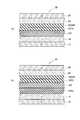
- FIG. 2 is a schematic cross-sectional structure diagram in which charging layers are multilayered in the secondary battery according to the first embodiment.
- the typical cross-section figure of the secondary battery which concerns on 2nd Embodiment.
- (A) The typical cross-section figure of the secondary battery which concerns on 3rd Embodiment
- (b) The typical cross-section figure of the secondary battery which concerns on the modification 1 of 3rd Embodiment.
- the typical cross-section figure of the secondary battery which concerns on the modification 2 of 3rd Embodiment.
- the first conductivity type indicates, for example, n-type
- the second conductivity type indicates p-type opposite to the first conductivity type
- FIG. 1 A schematic cross-sectional structure of the secondary battery 30 according to the first embodiment is expressed as shown in FIG. 1, and in the secondary battery 30 according to the first embodiment, a schematic diagram in which the charging layer 16T is multilayered.
- a typical cross-sectional structure is expressed as shown in FIG.
- the secondary battery 30 is laminated between a first electrode (E1) 12 and a second electrode (E2) 26, and is of a first conductivity type.
- First oxide semiconductor layer 14 first charge layer 16T disposed on first oxide semiconductor layer 14 and made of a first metal oxide, and first separation layer 18SNS disposed on first charge layer 16T And a second conductive type second oxide semiconductor layer 24 disposed on the first separation layer 18SNS.
- the first conductivity type first oxide semiconductor layer 14 is an oxide semiconductor layer made of the first conductivity type first oxide semiconductor.
- the second conductivity type second oxide semiconductor layer 24 is an oxide semiconductor layer made of the second conductivity type second oxide semiconductor. The same applies hereinafter.
- the first charging layer 16T is not made of a material containing silicon.
- the first separation layer 18SNS may include a first insulator.
- first separation layer 18SNS may further include an electrical conductivity adjusting material.
- the electrical conductivity adjusting material may include a first conductivity type semiconductor or a metal oxide.
- the electrical conductivity adjusting material may comprise at least one oxide selected from the group consisting of Sn, Zn, Ti, Al, Mg, or Nb oxides.
- the first insulator may include SiO x
- the electrical conductivity adjusting material may include SnO x .
- the first insulator may include SiO x formed from silicone oil.
- the first separation layer 18SNS may be mainly composed of SiO x .
- the first separation layer 18SNS may be mainly composed of SiO x and SnO x .
- the n-type oxide semiconductor layer 14 may be an oxide layer of titanium (Ti), tin (Sn), zinc (Zn), or magnesium (Mg).
- the first metal oxide may include at least one oxide selected from the group consisting of oxides of titanium (Ti), tin (Sn), zinc (Zn), and magnesium (Mg).
- the first charging layer 16T may include at least two layers having substantially the same composition.
- the first charging layer 16T as shown in FIG. 2, the composition is almost the same, the thin charge layer (TiO x) 16T 2, 16T 3, ..., may be formed by a stacked structure of 16T n.
- the first charging layer 16T When the first charging layer 16T is formed in a stacked structure in which the charging layers 16T 2 , 16T 3 ,..., 16T n are stacked, the first charging layer 16T can be formed without causing a fatal defect.
- the fatal defect is, for example, a pinhole penetrating the first charging layer 16T.
- the first charging layer 16T is formed in a stacked structure, for example, even if a pinhole is generated in an arbitrary layer constituting the first charging layer 16T, a pinhole is not generated in another layer. It is possible to prevent the occurrence of a pinhole (fatal defect) that penetrates the charging layer 16T.
- the first charging layer 16T may include at least two layers having different compositions.
- the first metal oxide may include titanium oxide (TiO x ). Therefore, the charging layer 16T may be formed by TiO x.
- first charging layer 16T may further include hydrogen.
- the first charging layer 16T may have a porous structure.
- the second oxide semiconductor layer 24 may be made of NiO x .
- the second oxide semiconductor layer 24 may further include hydrogen.
- the first charging layer 16T does not include a silicon oxide film, the internal resistance can be reduced and the battery performance is improved.
- the first separation layer 18SNS is desirably an insulating film that is permeable to hydrogen ions and that does not substantially conduct electrons. Further, it is possible to adjust the hydrogen ion permeation performance by further adding an electrical conductivity adjusting material to the first separation layer 18SNS.
- the first charging layer 16T is a layer that accumulates hydrogen generated during charging.
- a reaction of MO x + H 2 O + e ⁇ ⁇ MH + OH ⁇ proceeds during charging, and a reaction of MO x H + OH ⁇ ⁇ M + H 2 O + e ⁇ proceeds during discharging.
- the first metal oxide can be optimized by using an oxide of Ti, Sn, Zn, or Mg.
- the secondary battery 30 includes a first electrode 12 and a second electrode 26, and the first oxide semiconductor layer 14 includes an n-type oxide semiconductor layer.
- the first metal oxide comprises an n-type metal oxide
- the second oxide semiconductor layer 24 comprises a p-type second oxide semiconductor layer, and is connected to the second electrode 26. It may be connected.
- the method for manufacturing the secondary battery 30 according to the first embodiment includes a step of forming a first conductivity type first oxide semiconductor layer 14, and a first metal oxide on the first oxide semiconductor layer 14.
- Forming a first charging layer 16T comprising: forming a first separation layer 18SNS on the first charging layer 16T; forming a second oxide semiconductor layer 24 on the first separation layer 18SNS;
- the step of forming the second oxide semiconductor layer 24 uses a reactive sputtering technique in which a sputtering deposition method is applied, metallic nickel Ni is used as a target material during sputtering, and oxygen is added to the sputtering gas. May be used.
- -N-type oxide semiconductor layer 14- A TiO x film is formed on the first electrode 12 by, for example, a sputtering deposition method.
- Ti or TiO x can be used as a target.
- the film thickness of the n-type oxide semiconductor layer 14 is, for example, about 50 nm to 200 nm.
- a tungsten (W) electrode can be used as the first electrode 12.
- the first charging layer 16T is formed by applying a chemical solution on the n-type first oxide semiconductor layer 14 by a spin coating method. Specifically, the chemical solution is formed by stirring fatty acid titanium with a solvent. This chemical solution is applied onto the n-type oxide semiconductor layer 14 using a spin coater. The rotational speed is, for example, about 500 to 3000 rpm. After application, it is dried on a hot plate. The drying temperature on the hot plate is, for example, about 30 ° C.-200 ° C., and the drying time is, for example, about 5-30 minutes. Baking after drying. For the post-drying firing, firing is performed in the air using a firing furnace. The firing temperature is, for example, about 300 ° C. to 600 ° C., and the firing time is, for example, about 10 minutes to 60 minutes.
- hydrogen (H) may be added to TiO x constituting the charge layer 16T by firing in the atmosphere.
- the manufacturing (manufacturing) method in which titanium dioxide is layered is a coating pyrolysis method. After firing, UV irradiation with a low-pressure mercury lamp is performed. The UV irradiation time is, for example, about 10 to 100 minutes.
- the thickness of the first charging layer 16T is, for example, about 50 nm-200 nm. Alternatively, it may be formed in a laminated manner to make it thicker.
- the first separation layer 18SNS is formed by applying a chemical solution on the first charging layer 16T by a spin coating method. Specifically, the chemical solution is formed by stirring fatty acid tin and silicone oil together with a solvent. This chemical solution is applied onto the charging layer 16T using a spin coating device. The rotational speed is, for example, about 500 to 3000 rpm. After application, it is dried on a hot plate. The drying temperature on the hot plate is, for example, about 30 ° C.-200 ° C., and the drying time is, for example, about 5-30 minutes. Furthermore, it is fired after drying. For the post-drying firing, firing is performed in the air using a firing furnace. The firing temperature is, for example, about 300 ° C.
- the firing time is, for example, about 10 minutes to 60 minutes.
- UV irradiation with a low-pressure mercury lamp is performed.
- the UV irradiation time is, for example, about 10 to 100 minutes.
- the thickness of the separation layer 18SNS after UV irradiation is, for example, about 50 nm to 300 nm.
- a p-type oxide semiconductor layer (NiO) 24 is formed on the first separation layer 18SNS by, for example, a sputtering deposition method.
- Ni or NiO can be used as a target.
- Ni atoms are excited from the target by ion bombardment with argon ions Ar + , and the excited Ni atoms deposit the second oxide semiconductor layer 24 by sputter deposition reaction. May be formed.
- the second electrode 26 is formed by, for example, Al by sputtering deposition or vacuum deposition. A film can be formed on the p-type oxide semiconductor layer (NiO) 24 using an Al target.
- a stainless mask may be used, and only the designated region may be formed.
- the first embodiment it is possible to provide a secondary battery that can reduce internal resistance and increase the storage capacity per unit volume (weight).
- FIG. 3 A schematic cross-sectional structure of the secondary battery 30 according to the second embodiment is expressed as shown in FIG. 3, and in the secondary battery 30 according to the second embodiment, a schematic diagram in which the charging layer 16T is multilayered.
- the general cross-sectional structure is expressed in the same manner as in FIG.
- the secondary battery 30 is laminated between the first electrode (E1) 12 and the second electrode (E2) 26, and is of the first conductivity type.
- a second oxide semiconductor layer 24 of the second conductivity type disposed on the first separation layer 18S.
- the first charging layer 16T is not made of a material containing silicon.
- the first separation layer 18S may include a first insulator.
- the first separation layer 18S may be mainly composed of SiO x .
- the first insulator may include SiO x formed from silicone oil.
- the first insulator may include SiO x .
- the n-type first oxide semiconductor layer 14 may be an oxide layer of titanium (Ti), tin (Sn), zinc (Zn), or magnesium (Mg).
- the first metal oxide may include at least one oxide selected from the group consisting of oxides of titanium (Ti), tin (Sn), zinc (Zn), and magnesium (Mg).
- the first charging layer 16T may include at least two layers having substantially the same composition.
- the first charging layer 16T as shown in FIG. 2, the composition is almost the same, the thin charge layer (TiO x) 16T 2, 16T 3, ..., may be formed by a stacked structure of 16T n.
- the first charging layer 16T is formed in a stacked structure in which the charging layers 16T 2 , 16T 3 ,..., 16T n are stacked, the first charging layer 16T can be formed without causing a fatal defect.
- the first charging layer 16T may include at least two layers having different compositions.
- the first metal oxide may include titanium oxide (TiO x ). Therefore, the first charging layer 16T may be formed of TiO x .
- first charging layer 16T may further include hydrogen.
- the first charging layer 16T may have a porous structure.
- the second oxide semiconductor layer 24 may be made of NiO x .
- the second oxide semiconductor layer 24 may further include hydrogen.
- the first charging layer 16T does not include a silicon oxide film, the internal resistance can be reduced and the battery performance is improved.
- the separation layer 18S is desirably an insulating film that is permeable to hydrogen ions and that does not substantially conduct electrons.
- the first charging layer 16T is a layer that accumulates hydrogen generated during charging.
- a reaction of MO x + H 2 O + e ⁇ ⁇ MH + OH ⁇ proceeds during charging, and a reaction of MO x H + OH ⁇ ⁇ M + H 2 O + e ⁇ proceeds during discharging.
- the efficiency of hydrogen accumulation can be increased.
- hydrogen accumulation and conductivity can be optimized by using a plurality of layers.
- the first metal oxide as an oxide of Ti, Sn, Zn, or Mg, it is possible to optimize hydrogen accumulation and conductivity.
- the secondary battery 30 includes a first electrode 12 and a second electrode 26, and the first oxide semiconductor layer 14 includes an n-type oxide semiconductor layer.
- the first metal oxide comprises an n-type metal oxide
- the second oxide semiconductor layer 24 comprises a p-type second oxide semiconductor layer, and is connected to the second electrode 26. It may be connected.
- the manufacturing method of the secondary battery 30 according to the second embodiment includes a step of forming a first conductivity type first oxide semiconductor layer 14 and a first metal oxide on the first oxide semiconductor layer 14.
- the step of forming the second oxide semiconductor layer 24 uses a reactive sputtering technique in which a sputtering deposition method is applied, metallic nickel Ni is used as a target material during sputtering, and oxygen is added to the sputtering gas. May be used.
- -N-type oxide semiconductor layer 14- A TiO x film is formed on the first electrode 12 by, for example, a sputtering deposition method.
- Ti or TiO x can be used as a target.
- the film thickness of the n-type oxide semiconductor layer 14 is, for example, about 50 nm to 200 nm.
- a tungsten (W) electrode can be used as the first electrode 12.
- the first charging layer 16T is formed by applying a chemical solution on the n-type first oxide semiconductor layer 14 by a spin coating method. Specifically, the chemical solution is formed by stirring fatty acid titanium with a solvent. This chemical solution is applied onto the n-type oxide semiconductor layer 14 using a spin coater. The rotational speed is, for example, about 500 to 3000 rpm. After application, it is dried on a hot plate. The drying temperature on the hot plate is, for example, about 30 ° C.-200 ° C., and the drying time is, for example, about 5-30 minutes. Baking after drying. For the post-drying firing, firing is performed in the air using a firing furnace. The firing temperature is, for example, about 300 ° C. to 600 ° C., and the firing time is, for example, about 10 minutes to 60 minutes.
- hydrogen (H) may be added to TiO x constituting the first charge layer 16T by firing in the air.
- the manufacturing (manufacturing) method in which titanium dioxide is layered is a coating pyrolysis method. After firing, UV irradiation with a low-pressure mercury lamp is performed. The UV irradiation time is, for example, about 10 to 100 minutes.
- the thickness of the charging layer 16T is, for example, about 50 nm to 200 nm. Alternatively, it may be formed in a laminated manner to make it thicker.
- the first separation layer 18S is formed by applying a chemical solution on the first charging layer 16T by a spin coating method. Specifically, the chemical solution is formed by stirring silicone oil with a solvent. This chemical solution is applied onto the first charging layer 16T using a spin coating device. The rotational speed is, for example, about 500 to 3000 rpm. After application, it is dried on a hot plate. The drying temperature on the hot plate is, for example, about 50 ° C.-200 ° C., and the drying time is, for example, about 5-30 minutes. Furthermore, it is fired after drying. For the post-drying firing, firing is performed in the air using a firing furnace. The firing temperature is, for example, about 300 ° C.
- the firing time is, for example, about 10 minutes to 60 minutes.
- UV irradiation with a low-pressure mercury lamp is performed.
- the UV irradiation time is, for example, about 10-60 minutes.
- the thickness of the separation layer 18S after UV irradiation is, for example, about 5 nm-30 nm.
- a p-type oxide semiconductor layer (NiO) 24 is formed on the first separation layer 18S by, for example, a sputtering deposition method.
- Ni or NiO can be used as a target.
- Ni atoms are excited from the target by ion bombardment with argon ions Ar + , and the excited Ni atoms deposit the second oxide semiconductor layer 24 by sputter deposition reaction. May be formed.
- the second electrode 26 is formed by, for example, Al by sputtering deposition or vacuum deposition. A film can be formed on the p-type oxide semiconductor layer (NiO) 24 using an Al target.
- a stainless mask may be used, and only the designated region may be formed.
- battery performance equivalent to that of the first embodiment can be exhibited, and an equivalent energy density ratio can be obtained.
- the second embodiment it is possible to provide a secondary battery that can reduce internal resistance and increase the storage capacity per unit volume (weight).
- FIG. 4A A schematic cross-sectional structure of a secondary battery 30 according to the third embodiment is represented as shown in FIG. 4A, and a schematic cross-section of a secondary battery according to Modification 1 of the third embodiment.
- the structure is represented as shown in FIG.
- a schematic cross-sectional structure in which the first charging layer 16T is multilayered is expressed similarly to FIG.
- the secondary battery 30 is stacked between the first electrode (E1) 12 and the second electrode (E2) 26 as shown in FIG.
- the separation layer 18TS includes a first separation layer 18SNS disposed on the second separation layer 18TS, and a second conductivity type second oxide semiconductor layer 24 disposed on the first separation layer 18SNS.
- the secondary battery 30 according to the third embodiment is disposed on the first charging layer 16T between the first separation layer 18SNS and the first charging layer 16T.
- the second separation layer 18TS may be provided.
- the secondary battery 30 includes the first oxide semiconductor layer 14 and the first oxide semiconductor layer 14 on the first oxide semiconductor layer 14. You may provide 2nd charge layer 16TS which is arrange
- the first charging layer 16T is not made of a material containing silicon.
- the first separation layer 18SNS and the second separation layer 18TS may include a first insulator.
- first separation layer 18SNS may further include an electrical conductivity adjusting material.
- the electrical conductivity adjusting material may include a first conductivity type semiconductor or a metal oxide.
- the electrical conductivity adjusting material may comprise at least one oxide selected from the group consisting of Sn, Zn, Ti, Al, Mg, or Nb oxides.
- the first insulator may include SiO x
- the electrical conductivity adjusting material may include SnO x .
- the first insulators of the first separation layer 18SNS and the second separation layer 18TS may be mainly composed of SiO x formed from silicone oil.
- the separation layer may be composed mainly of SiO x and SnO x and mainly SiO x and TiO x . That is, for example, the first separation layer 18SNS may be mainly composed of SiO x and SnO x , and the second separation layer 18TS may be mainly composed of SiO x and TiO x .
- the second charge layer may be mainly composed of SiO x and TiO x .
- the n-type oxide semiconductor layer 14 may be an oxide layer of titanium (Ti), tin (Sn), zinc (Zn), or magnesium (Mg).
- the first metal oxide may include at least one oxide selected from the group consisting of oxides of titanium (Ti), tin (Sn), zinc (Zn), and magnesium (Mg).
- the first charging layer 16T may include at least two layers having substantially the same composition.
- the first charging layer 16T as shown in FIG. 2, the composition is almost the same, the thin charge layer (TiO x) 16T 2, 16T 3, ..., may be formed by a stacked structure of 16T n.
- the first charge layer 16T is formed in a stacked structure in which the charge layers 16T 2 , 16T 3 ,..., 16T n are stacked, the first charge layer 16T can be formed without causing a fatal defect.
- the first charging layer 16T may include at least two layers having different compositions.
- the first metal oxide may include titanium oxide (TiO x ). Therefore, the first charging layer 16T may be formed of TiO x .
- first charging layer 16T may further include hydrogen.
- the first charging layer 16T may have a porous structure.
- the second oxide semiconductor layer 24 may be made of NiO x .
- the second oxide semiconductor layer 24 may further include hydrogen.
- the first charging layer 16T does not include a silicon oxide film, the internal resistance can be reduced and the battery performance is improved.
- first separation layer 18SNS and the second separation layer 18TS are films that can transmit hydrogen ions and are insulating films that do not substantially conduct electrons.
- an electrical conductivity adjusting material may be further added to the first separation layer 18SNS to adjust the hydrogen ion permeation performance.
- the breakdown voltage can be improved, cycle deterioration can be improved, and natural discharge can be suppressed more favorably.
- the first charging layer 16T and the second charging layer 16TS are layers that accumulate hydrogen generated during charging.
- a reaction of MO x + H 2 O + e ⁇ ⁇ MH + OH ⁇ proceeds during charging, and a reaction of MO x H + OH ⁇ ⁇ M + H 2 O + e ⁇ proceeds during discharging. .
- the first metal oxide can be optimized by using an oxide of Ti, Sn, Zn, or Mg.
- the second charging layer is mainly composed of SiO x and TiO x .
- the secondary battery 30 includes the first electrode 12 and the second electrode 26,
- the first oxide semiconductor layer 14 includes an n-type oxide semiconductor layer and is connected to the first electrode 12, the first metal oxide includes an n-type metal oxide, and the second oxide semiconductor layer 24 includes a p-type first oxide layer.
- a two-oxide semiconductor layer may be provided and connected to the second electrode 26.
- the manufacturing method of the secondary battery 30 according to the third embodiment includes a step of forming a first conductivity type first oxide semiconductor layer 14, and a first metal oxide on the first oxide semiconductor layer 14.
- Forming a first charging layer 16T comprising: a step of forming a second separation layer 18TS on the first charging layer 16T; a step of forming a first separation layer 18SNS on the second separation layer 18TS; Forming a second oxide semiconductor layer 24 on the one isolation layer 18SNS.
- the first oxide semiconductor layer 14 is formed on the first oxide semiconductor layer 14 as shown in FIG. And a step of forming a second charging layer 16TS made of a second insulator and a second metal oxide, disposed between the first charging layer 16T and the first charging layer 16T.
- the step of forming the second oxide semiconductor layer 24 uses a reactive sputtering technique in which a sputtering deposition method is applied, metallic nickel Ni is used as a target material during sputtering, and oxygen is added to the sputtering gas. May be used.
- -N-type oxide semiconductor layer 14- A TiO x film is formed on the first electrode 12 by, for example, a sputtering deposition method.
- Ti or TiO x can be used as a target.
- the film thickness of the n-type oxide semiconductor layer 14 is, for example, about 50 nm to 200 nm.
- a tungsten (W) electrode can be used as the first electrode 12.
- the first charging layer 16T is formed by applying a chemical solution on the n-type oxide semiconductor layer 14 by a spin coating method. It is formed by coating.
- the first charging layer 16T has a chemical solution on the second charging layer 16TS. It is formed by applying by spin coating. Specifically, the chemical solution is formed by stirring fatty acid titanium with a solvent. This chemical solution is applied onto the n-type oxide semiconductor layer 14 using a spin coater. The rotational speed is, for example, about 500 to 3000 rpm.
- the drying temperature on the hot plate is, for example, about 30 ° C.-200 ° C., and the drying time is, for example, about 5-30 minutes.
- firing is performed in the air using a firing furnace.
- the firing temperature is, for example, about 300 ° C. to 600 ° C., and the firing time is, for example, about 10 minutes to 60 minutes.
- hydrogen (H) may be added to TiO x constituting the charge layer 16T by firing in the atmosphere.
- the manufacturing (manufacturing) method in which titanium dioxide is layered is a coating pyrolysis method. After firing, UV irradiation with a low-pressure mercury lamp is performed. The UV irradiation time is, for example, about 10 to 100 minutes.
- the thickness of the charging layer 16T is, for example, about 50 nm to 200 nm. Alternatively, it may be formed in a laminated manner to make it thicker.
- the second charging layer 16TS has a chemical solution on the n-type first oxide semiconductor layer 14 as shown in FIG. Is applied by spin coating.
- the chemical solution is formed by stirring fatty acid titanium and silicone oil together with a solvent.
- This chemical solution is applied onto the n-type oxide semiconductor layer 14 using a spin coater.
- the rotational speed is, for example, about 500 to 3000 rpm.
- After application it is dried on a hot plate.
- the drying temperature on the hot plate is, for example, about 30 ° C.-200 ° C., and the drying time is, for example, about 5-30 minutes. Baking after drying.
- firing is performed in the air using a firing furnace.
- the firing temperature is, for example, about 300 ° C. to 600 ° C.
- the firing time is, for example, about 10 minutes to 60 minutes.
- the aliphatic acid salt is decomposed to form a fine particle layer of titanium dioxide covered with a silicone insulating film.
- the above manufacturing (manufacturing) method in which titanium dioxide covered with a silicone insulating film is formed is a coating pyrolysis method. After firing, UV irradiation with a low-pressure mercury lamp is performed. The UV irradiation time is, for example, about 10 to 100 minutes. The film thickness of the second charging layer 16TS after UV irradiation is, for example, about 50 nm to 300 nm.
- the second separation layer 18TS is formed by applying a chemical solution on the first charging layer 16T by a spin coating method. Specifically, the chemical solution is formed by stirring fatty acid titanium and silicone oil together with a solvent. This chemical solution is applied onto the charging layer 16T using a spin coating device. The rotational speed is, for example, about 500 to 3000 rpm. After application, it is dried on a hot plate. The drying temperature on the hot plate is, for example, about 30 ° C.-200 ° C., and the drying time is, for example, about 5-30 minutes. Baking after drying. For the post-drying firing, firing is performed in the air using a firing furnace. The firing temperature is, for example, about 300 ° C. to 600 ° C., and the firing time is, for example, about 10 minutes to 60 minutes.
- the aliphatic acid salt is decomposed to form a fine particle layer of titanium dioxide covered with a silicone insulating film.
- the above manufacturing (manufacturing) method in which titanium dioxide covered with a silicone insulating film is formed is a coating pyrolysis method. After firing, UV irradiation with a low-pressure mercury lamp is performed. The UV irradiation time is, for example, about 10 to 100 minutes. The film thickness of the second separation layer 18TS after UV irradiation is, for example, about 5 nm-30 nm.
- the first separation layer 18SNS is formed by applying a chemical solution on the second separation layer 18TS by a spin coating method. Specifically, the chemical solution is formed by stirring fatty acid tin and silicone oil together with a solvent. This chemical solution is applied onto the charging layer 16T using a spin coating device. The rotational speed is, for example, about 500 to 3000 rpm. After application, it is dried on a hot plate. The drying temperature on the hot plate is, for example, about 30 ° C.-200 ° C., and the drying time is, for example, about 5-30 minutes. Furthermore, it is fired after drying. For the post-drying firing, firing is performed in the air using a firing furnace. The firing temperature is, for example, about 300 ° C.
- the firing time is, for example, about 10 minutes to 60 minutes.
- UV irradiation with a low-pressure mercury lamp is performed.
- the UV irradiation time is, for example, about 10 to 100 minutes.
- the film thickness of the first separation layer 18SNS after UV irradiation is, for example, about 5 nm-30 nm.
- a p-type oxide semiconductor layer (NiO x ) 24 is formed on the first separation layer 18SNS by, for example, a sputtering deposition method.
- Ni or NiO can be used as a target.
- Ni atoms are excited from the target by ion bombardment with argon ions Ar + , and the excited Ni atoms are sputtered by the second oxide semiconductor layer 24. May be deposited.
- the second electrode 26 is formed by, for example, Al by sputtering deposition or vacuum deposition.
- a film can be formed on the p-type oxide semiconductor layer (nickel oxide (NiO)) 24 using an Al target.
- a stainless mask may be used, and only the designated region may be formed.
- the breakdown voltage can be improved as compared to the first embodiment, and cycle deterioration is caused. Can be improved, and spontaneous discharge can be suppressed more satisfactorily.
- the secondary battery 30 includes a first oxide semiconductor layer 14 and a second insulator disposed on the first oxide semiconductor layer 14. And a second charging layer 16TS made of the second metal oxide, a first charging layer 16T made of the first metal oxide, and a second charging layer 16TS made of the first metal oxide.
- the first charging layer 16T is formed in a three-layer structure including charging layers 16T 1 , 16T 2 , and 16T 3 .
- charge layers 16T 1 , 16T 2 , and 16T 3 may have substantially the same composition.
- the first charging layer 16T may be formed by a laminated structure of thin charging layers (TiO x ) 16T 1 , 16T 2 , and 16T 3 having substantially the same composition.
- the first charging layer 16T can be formed without causing a fatal defect.
- charge layers 16T 1 , 16T 2 , and 16T 3 may have different compositions.
- the second charging layer 16TS and the second separation layer 18TSP made of the second insulator and the second metal oxide can be formed in the same manner as the second charging layer 16TS and the second separation layer 18TS in the third embodiment. .
- the second separation layer 18TSP and the first separation layer 18SNS are desirably films that are permeable to hydrogen ions and are insulating films that do not substantially conduct electrons. Other configurations are the same as those of the third embodiment.
- the second modification of the third embodiment it is possible to improve the yield and withstand voltage by multilayering the first charge layer, to improve cycle deterioration, and to improve the natural discharge. It can be suppressed.
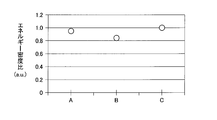
- each plot corresponding to A, B, and C on the horizontal axis represents the energy density ratio of the comparative example, the second embodiment, and the third embodiment, respectively.
- the secondary battery according to the comparative example corresponds to an example having the structure in which the first charging layer 16T is formed using fatty acid titanium and silicone oil in the secondary battery according to the first embodiment. Yes.
- the first separation layer / first charge layer has a structure of SnO x + SiO x / TiO x + SiO x .
- the first separation layer / first charge layer has a structure of SiO x / TiO x .
- the separation layer has a two-layer structure of SnO x + SiO x / TiO x + SiO x and the charging layer has a TiO x structure.
- the energy density ratio is as shown in FIG. As shown in FIG. 6, it is slightly lower than the comparative example (A).
- the silicone oil is drained in the formation of the first charging layer, and the separation layer has a two-layer structure of SnO x + SiO x / TiO x + SiO x . As shown in FIG. 6, a slightly higher energy density ratio is obtained as compared with the comparative example (A).
- the energy density ratio exhibits a flat characteristic even when the cycle number NC increases.
- the secondary battery (A) according to the comparative example uses silicone oil in the formation of the charge layer, the charge layer includes a SiO x layer. For this reason, the internal resistance of the charge layer is increased, which hinders battery performance such as cycle characteristics.
- a rechargeable battery according to a third embodiment (C) because of not using the silicone oil in the form of the charging layer, the charge layer is not included SiO x layer, it remains TiO x layer. For this reason, an increase in the internal resistance of the charge layer is suppressed, a good cycle characteristic is exhibited, and the battery performance is improved.
- the structure of the secondary battery 30 according to the embodiment is produced in a sheet shape using a stainless steel foil as a substrate. Thereafter, the sheets may be laminated to produce a secondary battery 30 having a necessary capacity.
- a secondary battery having a required capacity may be produced by facing the second electrodes of two sheets, inserting an electrode (thin metal foil) between them, and stacking the two sheets in multiple layers. . Thereafter, it may be sealed with a laminate or the like.
- the present embodiment includes various embodiments that are not described here.
- the secondary battery according to the present embodiment can be used for various consumer devices and industrial devices, and can be used for communication terminals, secondary batteries for wireless sensor networks, etc. It can be applied to a wide range of application fields such as secondary batteries.
Landscapes
- Chemical & Material Sciences (AREA)
- Chemical Kinetics & Catalysis (AREA)
- Electrochemistry (AREA)
- General Chemical & Material Sciences (AREA)
- Engineering & Computer Science (AREA)
- Manufacturing & Machinery (AREA)
- Inorganic Chemistry (AREA)
- Composite Materials (AREA)
- Materials Engineering (AREA)
- Battery Electrode And Active Subsutance (AREA)
- Secondary Cells (AREA)
- Cell Separators (AREA)
Abstract
Description
第1の実施の形態に係る二次電池30の模式的断面構造は、図1に示すように表され、第1の実施の形態に係る二次電池30において、充電層16Tを多層化した模式的断面構造は、図2に示すように表される。
第1分離層18SNSは、水素イオンを透過可能な膜であり、かつ電子を実質的に導通しない絶縁膜であることが望ましい。また、第1分離層18SNSには、更に電気導電率調整材を添加して、水素イオンの透過性能を調整可能である。
第1充電層16Tは、充電時に発生した水素を蓄積する層である。第1充電層16Tは、充電時は、MOx+H2O+e-→MH+OH-の反応が進行し、放電時は、MOxH+OH-→M+H2O+e-の反応が進行する。多孔質化することで、水素蓄積の効率を増大可能である。また、複数層とすることで、水素蓄積と導電性を最適化できる。第1金属酸化物を、Ti、Sn、Zn若しくはMgの酸化物とすることで、最適化可能である。
第1の実施の形態に係る二次電池30は、図1に示すように、第1電極12と、第2電極26とを備え、第1酸化物半導体層14はn型酸化物半導体層を備え、かつ第1電極12に接続され、第1金属酸化物はn型金属酸化物を備え、第2酸化物半導体層24はp型第2酸化物半導体層を備え、かつ第2電極26に接続されていても良い。
第1の実施の形態に係る二次電池30の製造方法は、第1導電型の第1酸化物半導体層14を形成する工程と、第1酸化物半導体層14上に、第1金属酸化物からなる第1充電層16Tを形成する工程と、第1充電層16T上に第1分離層18SNSを形成する工程と、第1分離層18SNS上に第2酸化物半導体層24を形成する工程とを有する。
第1電極12上にTiOx膜を例えば、スパッタデポジション法で成膜する。ここで、TiまたはTiOxをターゲットとして使用可能である。n型酸化物半導体層14の膜厚は、例えば、約50nm-200nm程度である。なお、第1電極12は、例えば、タングステン(W)電極などを適用可能である。
第1充電層16Tは、n型第1酸化物半導体層14上に薬液をスピンコート法で塗布することにより形成する。具体的に、薬液は脂肪酸チタンを溶媒と共に攪拌して形成する。この薬液を、スピン塗布装置を用いて、n型酸化物半導体層14上に塗布する。回転数は例えば、約500-3000rpmである。塗布後、ホットプレート上で乾燥させる。ホットプレート上の乾燥温度は、例えば、約30℃-200℃程度、乾燥時間は、例えば約5分-30分程度である。乾燥後焼成する。乾燥後焼成には、焼成炉を用い、大気中で焼成する。焼成温度は例えば、約300℃-600℃程度、焼成時間は例えば、約10分-60分程度である。ここで、大気中で焼成することにより、充電層16Tを構成するTiOxには、水素(H)が添加されていても良い。
第1分離層18SNSは、第1充電層16T上に薬液をスピンコート法で塗布することにより形成する。具体的に、薬液は脂肪酸スズとシリコーンオイルを溶媒と共に攪拌して形成する。この薬液を、スピン塗布装置を用いて、充電層16T上に塗布する。回転数は例えば、約500-3000rpmである。塗布後、ホットプレート上で乾燥させる。ホットプレート上の乾燥温度は例えば、約30℃-200℃程度、乾燥時間は例えば、約5分-30分程度である。さらに、乾燥後焼成する。乾燥後焼成には、焼成炉を用い、大気中で焼成する。焼成温度は例えば、約300℃-600℃程度、焼成時間は例えば、約10分-60分程度である。焼成後、低圧水銀ランプによるUV照射を実施する。UV照射時間は例えば、約10分-100分程度である。UV照射後の分離層18SNSの膜厚は、例えば、約50nm-300nm程度である。
第1分離層18SNS上にp型酸化物半導体層(NiO)24を例えば、スパッタデポジション法で成膜する。ここで、NiまたはNiOをターゲットとして使用可能である。第2酸化物半導体層24は、アルゴンイオンAr+によるイオン衝撃によって、ターゲットからNi原子が励起されると共に、励起されたNi原子は、スパッタデポジション反応により、第2酸化物半導体層24を堆積して形成しても良い。
第2電極26は、例えばAlをスパッタデポジション法若しくは真空蒸着法で成膜する。p型酸化物半導体層(NiO)24上にAlターゲットを使用して成膜可能である。第2電極26は、例えば、ステンレスマスクを用い、指定領域のみ成膜しても良い。
第2の実施の形態に係る二次電池30の模式的断面構造は、図3に示すように表され、第2の実施の形態に係る二次電池30において、充電層16Tを多層化した模式的断面構造は、図2と同様に表される。
分離層18Sは、水素イオンを透過可能な膜であり、かつ電子を実質的に導通しない絶縁膜であることが望ましい。
第1充電層16Tは、充電時に発生した水素を蓄積する層である。第1充電層16Tは、充電時は、MOx+H2O+e-→MH+OH-の反応が進行し、放電時は、MOxH+OH-→M+H2O+e-の反応が進行する。多孔質化することで、水素蓄積の効率を増大可能である。また、複数層とすることで、水素蓄積と導電性を最適化できる。第1金属酸化物を、Ti、Sn、Zn若しくはMgの酸化物とすることで、水素蓄積と導電性を最適化可能である。
第2の実施の形態に係る二次電池30は、図3に示すように、第1電極12と、第2電極26とを備え、第1酸化物半導体層14はn型酸化物半導体層を備え、かつ第1電極12に接続され、第1金属酸化物はn型金属酸化物を備え、第2酸化物半導体層24はp型第2酸化物半導体層を備え、かつ第2電極26に接続されていても良い。
第2の実施の形態に係る二次電池30の製造方法は、第1導電型の第1酸化物半導体層14を形成する工程と、第1酸化物半導体層14上に、第1金属酸化物からなる充電層16Tを形成する工程と、充電層16T上に分離層18Sを形成する工程と、分離層18S上に第2酸化物半導体層24を形成する工程とを有する。
第1電極12上にTiOx膜を例えば、スパッタデポジション法で成膜する。ここで、TiまたはTiOxをターゲットとして使用可能である。n型酸化物半導体層14の膜厚は、例えば、約50nm-200nm程度である。なお、第1電極12は、例えば、タングステン(W)電極などを適用可能である。
第1充電層16Tは、n型第1酸化物半導体層14上に薬液をスピンコート法で塗布することにより形成する。具体的に、薬液は脂肪酸チタンを溶媒と共に攪拌して形成する。この薬液を、スピン塗布装置を用いて、n型酸化物半導体層14上に塗布する。回転数は例えば、約500-3000rpmである。塗布後、ホットプレート上で乾燥させる。ホットプレート上の乾燥温度は、例えば、約30℃-200℃程度、乾燥時間は、例えば約5分-30分程度である。乾燥後焼成する。乾燥後焼成には、焼成炉を用い、大気中で焼成する。焼成温度は例えば、約300℃-600℃程度、焼成時間は例えば、約10分-60分程度である。ここで、大気中で焼成することにより、第1充電層16Tを構成するTiOxには、水素(H)が添加されていても良い。
第1分離層18Sは、第1充電層16T上に薬液をスピンコート法で塗布することにより形成する。具体的に、薬液はシリコーンオイルを溶媒と共に攪拌して形成する。この薬液を、スピン塗布装置を用いて、第1充電層16T上に塗布する。回転数は例えば、約500-3000rpmである。塗布後、ホットプレート上で乾燥させる。ホットプレート上の乾燥温度は例えば、約50℃-200℃程度、乾燥時間は例えば、約5分-30分程度である。さらに、乾燥後焼成する。乾燥後焼成には、焼成炉を用い、大気中で焼成する。焼成温度は例えば、約300℃-600℃程度、焼成時間は例えば、約10分-60分程度である。焼成後、低圧水銀ランプによるUV照射を実施する。UV照射時間は例えば、約10分-60分程度である。UV照射後の分離層18Sの膜厚は、例えば、約5nm-30nm程度である。
第1分離層18S上にp型酸化物半導体層(NiO)24を例えば、スパッタデポジション法で成膜する。ここで、NiまたはNiOをターゲットとして使用可能である。第2酸化物半導体層24は、アルゴンイオンAr+によるイオン衝撃によって、ターゲットからNi原子が励起されると共に、励起されたNi原子は、スパッタデポジション反応により、第2酸化物半導体層24を堆積して形成しても良い。
第2電極26は、例えばAlをスパッタデポジション法若しくは真空蒸着法で成膜する。p型酸化物半導体層(NiO)24上にAlターゲットを使用して成膜可能である。第2電極26は、例えば、ステンレスマスクを用い、指定領域のみ成膜しても良い。
第3の実施の形態に係る二次電池30の模式的断面構造は、図4(a)に示すように表され、第3の実施の形態の変形例1に係る二次電池の模式的断面構造は、図4(b)に示すように表される。第3の実施の形態およびその変形例1に係る二次電池30において、第1充電層16Tを多層化した模式的断面構造は、図2と同様に表される。
第1分離層18SNSおよび第2分離層18TSは、水素イオンを透過可能な膜であり、かつ電子を実質的に導通しない絶縁膜であることが望ましい。また、第1分離層18SNSには、更に電気導電率調整材を添加して、水素イオンの透過性能を調整しても良い。
第1充電層16T及び第2充電層16TSは、充電時に発生した水素を蓄積する層である。第1充電層16T及び第2充電層16TSは、充電時は、MOx+H2O+e-→MH+OH-の反応が進行し、放電時は、MOxH+OH-→M+H2O+e-の反応が進行する。多孔質化することで、水素蓄積の効率を増大可能である。また、複数層とすることで、水素蓄積と導電性を最適化できる。第1金属酸化物を、Ti、Sn、Zn若しくはMgの酸化物とすることで、最適化可能である。また、第2充電層は、SiOxとTiOxを主体に構成される。
第3の実施の形態およびその変形例1に係る二次電池30は、図4(a)および図4(b)に示すように、第1電極12と、第2電極26とを備え、第1酸化物半導体層14はn型酸化物半導体層を備え、かつ第1電極12に接続され、第1金属酸化物はn型金属酸化物を備え、第2酸化物半導体層24はp型第2酸化物半導体層を備え、かつ第2電極26に接続されていても良い。
第3の実施の形態に係る二次電池30の製造方法は、第1導電型の第1酸化物半導体層14を形成する工程と、第1酸化物半導体層14上に、第1金属酸化物からなる第1充電層16Tを形成する工程と、第1充電層16T上に第2分離層18TSを形成する工程と、第2分離層18TS上に第1分離層18SNSを形成する工程と、第1分離層18SNS上に第2酸化物半導体層24を形成する工程とを有する。
第1電極12上にTiOx膜を例えば、スパッタデポジション法で成膜する。ここで、TiまたはTiOxをターゲットとして使用可能である。n型酸化物半導体層14の膜厚は、例えば、約50nm-200nm程度である。なお、第1電極12は、例えば、タングステン(W)電極などを適用可能である。
第3の実施の形態に係る二次電池30の製造方法においては、図4(a)に示すように、第1充電層16Tは、n型酸化物半導体層14上に薬液をスピンコート法で塗布することにより形成する。また、第3の実施の形態の変形例1に係る二次電池30の製造方法においては、図4(b)に示すように、第1充電層16Tは、第2充電層16TS上に薬液をスピンコート法で塗布することにより形成する。具体的に、薬液は脂肪酸チタンを溶媒と共に攪拌して形成する。この薬液を、スピン塗布装置を用いて、n型酸化物半導体層14上に塗布する。回転数は例えば、約500-3000rpmである。塗布後、ホットプレート上で乾燥させる。ホットプレート上の乾燥温度は、例えば、約30℃-200℃程度、乾燥時間は、例えば約5分-30分程度である。乾燥後焼成する。乾燥後焼成には、焼成炉を用い、大気中で焼成する。焼成温度は例えば、約300℃-600℃程度、焼成時間は例えば、約10分-60分程度である。ここで、大気中で焼成することにより、充電層16Tを構成するTiOxには、水素(H)が添加されていても良い。
第3の実施の形態の変形例1に係る二次電池30の製造方法において、第2充電層16TSは、図4(b)に示すように、n型第1酸化物半導体層14上に薬液をスピンコート法で塗布することにより形成する。具体的に、薬液は脂肪酸チタンとシリコーンオイルを溶媒と共に攪拌して形成する。この薬液を、スピン塗布装置を用いて、n型酸化物半導体層14上に塗布する。回転数は例えば、約500-3000rpmである。塗布後、ホットプレート上で乾燥させる。ホットプレート上の乾燥温度は、例えば、約30℃-200℃程度、乾燥時間は、例えば約5分-30分程度である。乾燥後焼成する。乾燥後焼成には、焼成炉を用い、大気中で焼成する。焼成温度は例えば、約300℃-600℃程度、焼成時間は例えば、約10分-60分程度である。
第2分離層18TSは、第1充電層16T上に薬液をスピンコート法で塗布することにより形成する。具体的に、薬液は脂肪酸チタンとシリコーンオイルを溶媒と共に攪拌して形成する。この薬液を、スピン塗布装置を用いて、充電層16T上に塗布する。回転数は例えば、約500-3000rpmである。塗布後、ホットプレート上で乾燥させる。ホットプレート上の乾燥温度は、例えば、約30℃-200℃程度、乾燥時間は、例えば約5分-30分程度である。乾燥後焼成する。乾燥後焼成には、焼成炉を用い、大気中で焼成する。焼成温度は例えば、約300℃-600℃程度、焼成時間は例えば、約10分-60分程度である。
第1分離層18SNSは、第2分離層18TS上に薬液をスピンコート法で塗布することにより形成する。具体的に、薬液は脂肪酸スズとシリコーンオイルを溶媒と共に攪拌して形成する。この薬液を、スピン塗布装置を用いて、充電層16T上に塗布する。回転数は例えば、約500-3000rpmである。塗布後、ホットプレート上で乾燥させる。ホットプレート上の乾燥温度は例えば、約30℃-200℃程度、乾燥時間は例えば、約5分-30分程度である。さらに、乾燥後焼成する。乾燥後焼成には、焼成炉を用い、大気中で焼成する。焼成温度は例えば、約300℃-600℃程度、焼成時間は例えば、約10分-60分程度である。焼成後、低圧水銀ランプによるUV照射を実施する。UV照射時間は例えば、約10分-100分程度である。UV照射後の第1分離層18SNSの膜厚は、例えば、約5nm-30nm程度である。
第1分離層18SNS上にp型酸化物半導体層(NiOx)24を例えば、スパッタデポジション法で成膜する。ここで、NiまたはNiOをターゲットとして使用可能である。p型第2酸化物半導体層24は、アルゴンイオンAr+によるイオン衝撃によって、ターゲットからNi原子が励起されると共に、励起されたNi原子は、スパッタデポジション反応により、第2酸化物半導体層24を堆積して形成しても良い。
第2電極26は、例えばAlをスパッタデポジション法若しくは真空蒸着法で成膜する。p型酸化物半導体層(酸化ニッケル(NiO))24上にAlターゲットを使用して成膜可能である。第2電極26は、例えば、ステンレスマスクを用い、指定領域のみ成膜しても良い。
第3の実施の形態の変形例2に係る二次電池30の模式的断面構造は、図5に示すように表される。
比較例、第2の実施の形態および第3の実施の形態に係る二次電池のエネルギー密度比の特性比較例は、図6に示すように表される。
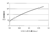
ここで、充電層の形成時に使用するシリコーンオイル量Csと充電層の内部抵抗との関係を示すデータ例は、図7に示すように表される。シリコーンオイル量Csの増加と共に、充電層の内部抵抗(充電層抵抗)は、増加する傾向が見られる。シリコーンオイル量Csがゼロのデータが第3の実施の形態に係る二次電池の充電層抵抗に対応する。
第3の実施の形態に係る二次電池(C)と比較例に係る二次電池(A)において、エネルギー密度比とサイクル回数NCとの関係(サイクル特性評価電力密度比較)を示すデータ例は、図8に示すように表される。
上記のように、いくつかの実施の形態について記載したが、開示の一部をなす論述及び図面は例示的なものであり、限定するものであると理解すべきではない。この開示から当業者には様々な代替実施の形態、実施例及び運用技術が明らかとなろう。
14…第1酸化物半導体層
16T、16TS、16T1、16T2、16T3、…、16Tn…充電層
18SNS、18S、18TS、18TSP…分離層
24…第2酸化物半導体層
26…第2電極(E2)
30…二次電池
Claims (19)
- 第1導電型の第1酸化物半導体層と、
前記第1酸化物半導体層上に配置され、第1金属酸化物からなる第1充電層と、
前記第1充電層上に配置された第1分離層と、
前記第1分離層上に配置された第2導電型の第2酸化物半導体層と
を備えることを特徴とする二次電池。 - 前記第1充電層は、シリコンを含む材料で構成されないことを特徴とする請求項1に記載の二次電池。
- 前記第1充電層上に、前記第1分離層と前記第1充電層との間に配置された第2分離層を備えることを特徴とする請求項1に記載の二次電池。
- 前記第1酸化物半導体層上に、前記第1酸化物半導体層と前記第1充電層との間に配置された、第2絶縁物と第2金属酸化物からなる第2充電層を備えることを特徴とする請求項1~3のいずれか1項に記載の二次電池。
- 前記第1充電層は、組成がほぼ同じ層を少なくとも2層備えることを特徴とする請求項1~4のいずれか1項に記載の二次電池。
- 前記第1充電層は、組成が互いに相違する層を少なくとも2層を備えることを特徴とする請求項1~4のいずれか1項に記載の二次電池。
- 前記第1分離層は、第1絶縁物を備えることを特徴とする請求項1~6いずれか1項に記載の二次電池。
- 前記第1分離層は、更に電気導電率調整材を備えることを特徴とする請求項7に記載の二次電池。
- 前記電気導電率調整材は、第1導電型の半導体、若しくは金属の酸化物を備えることを特徴とする請求項8に記載の二次電池。
- 前記電気導電率調整材は、Sn、Zn、Ti、Al、Mg、若しくはNbの酸化物からなる群から選択された少なくとも1つの酸化物を備えることを特徴とする請求項8または9に記載の二次電池。
- 前記第1絶縁物はSiOxを備え、前記電気導電率調整材はSnOxを備えることを特徴とする請求項8に記載の二次電池。
- 前記第1分離層は、SiOxを主体に構成されることを特徴とする請求項1~11のいずれか1項に記載の二次電池。
- 前記第1分離層は、SiOxとSnOxを主体に構成されることを特徴とする請求項1~11のいずれか1項に記載の二次電池。
- 前記第1分離層はSiOxとSnOxを主体に構成され、前記第2分離層はSiOxとTiOxを主体に構成されることを特徴とする請求項3に記載の二次電池。
- 前記第1金属酸化物は、Ti、Sn、Zn、若しくはMgの酸化物からなる群から選択された少なくとも1つの酸化物を備えることを特徴とする請求項1~14のいずれか1項に記載の二次電池。
- 前記第1金属酸化物は、TiOxを備えることを特徴とする請求項1~14のいずれか1項に記載の二次電池。
- 前記第2酸化物半導体層は、NiOxから構成されることを特徴とする請求項1~16のいずれか1項に記載の二次電池。
- 前記第2酸化物半導体層は、更に水素を備えることを特徴とする請求項17に記載の二次電池。
- 前記第2充電層は、SiOxとTiOxを主体に構成されることを特徴とする請求項4に記載の二次電池。
Priority Applications (5)
| Application Number | Priority Date | Filing Date | Title |
|---|---|---|---|
| CN201880018529.2A CN110431707A (zh) | 2017-03-16 | 2018-03-01 | 二次电池 |
| KR1020197027264A KR102280737B1 (ko) | 2017-03-16 | 2018-03-01 | 이차 전지 |
| CA3056195A CA3056195A1 (en) | 2017-03-16 | 2018-03-01 | Oxide semiconductor secondary battery |
| EP18766717.5A EP3598562A4 (en) | 2017-03-16 | 2018-03-01 | SECONDARY BATTERY |
| US16/569,340 US20200006764A1 (en) | 2017-03-16 | 2019-09-12 | Secondary battery |
Applications Claiming Priority (2)
| Application Number | Priority Date | Filing Date | Title |
|---|---|---|---|
| JP2017-051499 | 2017-03-16 | ||
| JP2017051499A JP7023049B2 (ja) | 2017-03-16 | 2017-03-16 | 二次電池 |
Related Child Applications (1)
| Application Number | Title | Priority Date | Filing Date |
|---|---|---|---|
| US16/569,340 Continuation US20200006764A1 (en) | 2017-03-16 | 2019-09-12 | Secondary battery |
Publications (1)
| Publication Number | Publication Date |
|---|---|
| WO2018168495A1 true WO2018168495A1 (ja) | 2018-09-20 |
Family
ID=63523421
Family Applications (1)
| Application Number | Title | Priority Date | Filing Date |
|---|---|---|---|
| PCT/JP2018/007775 WO2018168495A1 (ja) | 2017-03-16 | 2018-03-01 | 二次電池 |
Country Status (8)
| Country | Link |
|---|---|
| US (1) | US20200006764A1 (ja) |
| EP (1) | EP3598562A4 (ja) |
| JP (1) | JP7023049B2 (ja) |
| KR (1) | KR102280737B1 (ja) |
| CN (1) | CN110431707A (ja) |
| CA (1) | CA3056195A1 (ja) |
| TW (1) | TWI665817B (ja) |
| WO (1) | WO2018168495A1 (ja) |
Families Citing this family (1)
| Publication number | Priority date | Publication date | Assignee | Title |
|---|---|---|---|---|
| JP7122981B2 (ja) * | 2019-01-31 | 2022-08-22 | 株式会社日本マイクロニクス | 二次電池 |
Citations (11)
| Publication number | Priority date | Publication date | Assignee | Title |
|---|---|---|---|---|
| JPS558542B2 (ja) | 1975-07-17 | 1980-03-04 | ||
| JP5297809B2 (ja) | 2006-11-02 | 2013-09-25 | グエラテクノロジー株式会社 | 電界感応素子およびそれを用いた表示デバイス |
| JP2015082445A (ja) | 2013-10-23 | 2015-04-27 | 旭化成株式会社 | 二次電池 |
| JP2016082125A (ja) | 2014-10-20 | 2016-05-16 | パナソニックIpマネジメント株式会社 | 蓄電素子及び蓄電素子の製造方法 |
| JP2016127166A (ja) * | 2015-01-05 | 2016-07-11 | パナソニックIpマネジメント株式会社 | 蓄電素子およびその製造方法 |
| WO2016208116A1 (ja) * | 2015-06-25 | 2016-12-29 | 株式会社日本マイクロニクス | 二次電池の製造方法 |
| JP2017182969A (ja) * | 2016-03-29 | 2017-10-05 | イムラ・ジャパン株式会社 | 二次電池及びその製造方法 |
| JP2017195283A (ja) * | 2016-04-20 | 2017-10-26 | グエラテクノロジー株式会社 | 固体二次電池 |
| WO2017199618A1 (ja) * | 2016-05-19 | 2017-11-23 | 株式会社日本マイクロニクス | 二次電池の製造方法 |
| JP2018022719A (ja) * | 2016-08-01 | 2018-02-08 | 株式会社日本マイクロニクス | 二次電池 |
| JP2018037261A (ja) * | 2016-08-31 | 2018-03-08 | 株式会社日本マイクロニクス | 二次電池 |
Family Cites Families (5)
| Publication number | Priority date | Publication date | Assignee | Title |
|---|---|---|---|---|
| CN1172398C (zh) * | 2002-06-05 | 2004-10-20 | 郑洁洪 | 在铅蓄电池中使用的无硅胶体电解液 |
| FR2873460B1 (fr) * | 2004-07-21 | 2006-10-06 | Saint Gobain | Systeme electrochimique a electrolyte non oxyde |
| EP2626909B1 (en) * | 2010-10-07 | 2016-09-14 | Guala Technology Co., Ltd. | Secondary cell |
| JP2016014128A (ja) | 2014-06-09 | 2016-01-28 | 出光興産株式会社 | 二次電池及びそれに用いる構造体 |
| JP6656848B2 (ja) * | 2015-08-31 | 2020-03-04 | 株式会社日本マイクロニクス | 酸化物半導体二次電池の製造方法 |
-
2017
- 2017-03-16 JP JP2017051499A patent/JP7023049B2/ja active Active
-
2018
- 2018-03-01 EP EP18766717.5A patent/EP3598562A4/en not_active Withdrawn
- 2018-03-01 KR KR1020197027264A patent/KR102280737B1/ko active IP Right Grant
- 2018-03-01 CN CN201880018529.2A patent/CN110431707A/zh active Pending
- 2018-03-01 WO PCT/JP2018/007775 patent/WO2018168495A1/ja unknown
- 2018-03-01 CA CA3056195A patent/CA3056195A1/en not_active Abandoned
- 2018-03-12 TW TW107108266A patent/TWI665817B/zh active
-
2019
- 2019-09-12 US US16/569,340 patent/US20200006764A1/en not_active Abandoned
Patent Citations (11)
| Publication number | Priority date | Publication date | Assignee | Title |
|---|---|---|---|---|
| JPS558542B2 (ja) | 1975-07-17 | 1980-03-04 | ||
| JP5297809B2 (ja) | 2006-11-02 | 2013-09-25 | グエラテクノロジー株式会社 | 電界感応素子およびそれを用いた表示デバイス |
| JP2015082445A (ja) | 2013-10-23 | 2015-04-27 | 旭化成株式会社 | 二次電池 |
| JP2016082125A (ja) | 2014-10-20 | 2016-05-16 | パナソニックIpマネジメント株式会社 | 蓄電素子及び蓄電素子の製造方法 |
| JP2016127166A (ja) * | 2015-01-05 | 2016-07-11 | パナソニックIpマネジメント株式会社 | 蓄電素子およびその製造方法 |
| WO2016208116A1 (ja) * | 2015-06-25 | 2016-12-29 | 株式会社日本マイクロニクス | 二次電池の製造方法 |
| JP2017182969A (ja) * | 2016-03-29 | 2017-10-05 | イムラ・ジャパン株式会社 | 二次電池及びその製造方法 |
| JP2017195283A (ja) * | 2016-04-20 | 2017-10-26 | グエラテクノロジー株式会社 | 固体二次電池 |
| WO2017199618A1 (ja) * | 2016-05-19 | 2017-11-23 | 株式会社日本マイクロニクス | 二次電池の製造方法 |
| JP2018022719A (ja) * | 2016-08-01 | 2018-02-08 | 株式会社日本マイクロニクス | 二次電池 |
| JP2018037261A (ja) * | 2016-08-31 | 2018-03-08 | 株式会社日本マイクロニクス | 二次電池 |
Non-Patent Citations (1)
| Title |
|---|
| See also references of EP3598562A4 |
Also Published As
| Publication number | Publication date |
|---|---|
| JP2018156778A (ja) | 2018-10-04 |
| CN110431707A (zh) | 2019-11-08 |
| EP3598562A4 (en) | 2020-12-16 |
| JP7023049B2 (ja) | 2022-02-21 |
| EP3598562A1 (en) | 2020-01-22 |
| KR20190119628A (ko) | 2019-10-22 |
| TW201840055A (zh) | 2018-11-01 |
| KR102280737B1 (ko) | 2021-07-23 |
| TWI665817B (zh) | 2019-07-11 |
| CA3056195A1 (en) | 2018-09-20 |
| US20200006764A1 (en) | 2020-01-02 |
Similar Documents
| Publication | Publication Date | Title |
|---|---|---|
| EP1427042B1 (en) | Solid electrolyte with incorporated nitrogen and battery employing the same | |
| KR100359055B1 (ko) | 박막형 슈퍼 캐패시터 및 그 제조방법 | |
| JP5697931B2 (ja) | 電気化学キャパシタ | |
| JP2017529662A (ja) | 界面の抵抗及び過電圧を減少させるための中間層を含む電気化学デバイススタック | |
| JP5595349B2 (ja) | リチウムイオン二次電池用正極集電体、リチウムイオン二次電池用正極およびリチウムイオン二次電池用正極集電体の製造方法 | |
| KR20030017944A (ko) | 리튬 2차 전지용 음극 박막 및 그의 제조방법 | |
| CN1836338A (zh) | 新型金属带产品 | |
| TWI461555B (zh) | 一種多層膜矽/石墨烯複合材料陽極結構 | |
| KR20120080575A (ko) | 레독스 커패시터 및 그 제작 방법 | |
| WO2018042945A1 (ja) | 二次電池 | |
| WO2018095845A1 (en) | Li-ion based electrochemical energy storage cell | |
| KR100790844B1 (ko) | 박막 전지 및 그 제조 방법 | |
| WO2018168495A1 (ja) | 二次電池 | |
| US20200006763A1 (en) | Electricity storage device | |
| KR100563081B1 (ko) | 리튬 이차 전지용 음극 박막 및 그의 제조 방법 | |
| JP2010225356A (ja) | 非水電解質電池及びその使用方法 | |
| TWI728676B (zh) | 二次電池 | |
| WO2019181314A1 (ja) | 二次電池、及びその製造方法 | |
| WO2023238379A1 (ja) | リチウム二次電池、及び、リチウム二次電池の製造方法 | |
| KR20100063194A (ko) | 리튬 이차 전지용 음극 | |
| KR20200050270A (ko) | 다층 구조의 고체 전해질 및 이를 포함하는 전고체 박막 전지 | |
| JP2018088355A (ja) | 薄膜リチウム二次電池及びその製造方法 |
Legal Events
| Date | Code | Title | Description |
|---|---|---|---|
| 121 | Ep: the epo has been informed by wipo that ep was designated in this application |
Ref document number: 18766717 Country of ref document: EP Kind code of ref document: A1 |
|
| ENP | Entry into the national phase |
Ref document number: 3056195 Country of ref document: CA |
|
| NENP | Non-entry into the national phase |
Ref country code: DE |
|
| ENP | Entry into the national phase |
Ref document number: 20197027264 Country of ref document: KR Kind code of ref document: A |
|
| ENP | Entry into the national phase |
Ref document number: 2018766717 Country of ref document: EP Effective date: 20191016 |