WO2017199679A1 - 半導体装置 - Google Patents
半導体装置 Download PDFInfo
- Publication number
- WO2017199679A1 WO2017199679A1 PCT/JP2017/015874 JP2017015874W WO2017199679A1 WO 2017199679 A1 WO2017199679 A1 WO 2017199679A1 JP 2017015874 W JP2017015874 W JP 2017015874W WO 2017199679 A1 WO2017199679 A1 WO 2017199679A1
- Authority
- WO
- WIPO (PCT)
- Prior art keywords
- layer
- carrier injection
- drift
- injection layer
- electrode
- Prior art date
- Legal status (The legal status is an assumption and is not a legal conclusion. Google has not performed a legal analysis and makes no representation as to the accuracy of the status listed.)
- Ceased
Links
Images


Classifications
-
- H—ELECTRICITY
- H10—SEMICONDUCTOR DEVICES; ELECTRIC SOLID-STATE DEVICES NOT OTHERWISE PROVIDED FOR
- H10D—INORGANIC ELECTRIC SEMICONDUCTOR DEVICES
- H10D8/00—Diodes
-
- H—ELECTRICITY
- H10—SEMICONDUCTOR DEVICES; ELECTRIC SOLID-STATE DEVICES NOT OTHERWISE PROVIDED FOR
- H10D—INORGANIC ELECTRIC SEMICONDUCTOR DEVICES
- H10D12/00—Bipolar devices controlled by the field effect, e.g. insulated-gate bipolar transistors [IGBT]
- H10D12/411—Insulated-gate bipolar transistors [IGBT]
- H10D12/441—Vertical IGBTs
- H10D12/461—Vertical IGBTs having non-planar surfaces, e.g. having trenches, recesses or pillars in the surfaces of the emitter, base or collector regions
- H10D12/481—Vertical IGBTs having non-planar surfaces, e.g. having trenches, recesses or pillars in the surfaces of the emitter, base or collector regions having gate structures on slanted surfaces, on vertical surfaces, or in grooves, e.g. trench gate IGBTs
-
- H—ELECTRICITY
- H10—SEMICONDUCTOR DEVICES; ELECTRIC SOLID-STATE DEVICES NOT OTHERWISE PROVIDED FOR
- H10D—INORGANIC ELECTRIC SEMICONDUCTOR DEVICES
- H10D62/00—Semiconductor bodies, or regions thereof, of devices having potential barriers
- H10D62/10—Shapes, relative sizes or dispositions of the regions of the semiconductor bodies; Shapes of the semiconductor bodies
- H10D62/102—Constructional design considerations for preventing surface leakage or controlling electric field concentration
-
- H—ELECTRICITY
- H10—SEMICONDUCTOR DEVICES; ELECTRIC SOLID-STATE DEVICES NOT OTHERWISE PROVIDED FOR
- H10D—INORGANIC ELECTRIC SEMICONDUCTOR DEVICES
- H10D62/00—Semiconductor bodies, or regions thereof, of devices having potential barriers
- H10D62/10—Shapes, relative sizes or dispositions of the regions of the semiconductor bodies; Shapes of the semiconductor bodies
- H10D62/117—Shapes of semiconductor bodies
- H10D62/118—Nanostructure semiconductor bodies
- H10D62/119—Nanowire, nanosheet or nanotube semiconductor bodies
- H10D62/122—Nanowire, nanosheet or nanotube semiconductor bodies oriented at angles to substrates, e.g. perpendicular to substrates
-
- H—ELECTRICITY
- H10—SEMICONDUCTOR DEVICES; ELECTRIC SOLID-STATE DEVICES NOT OTHERWISE PROVIDED FOR
- H10D—INORGANIC ELECTRIC SEMICONDUCTOR DEVICES
- H10D62/00—Semiconductor bodies, or regions thereof, of devices having potential barriers
- H10D62/10—Shapes, relative sizes or dispositions of the regions of the semiconductor bodies; Shapes of the semiconductor bodies
- H10D62/13—Semiconductor regions connected to electrodes carrying current to be rectified, amplified or switched, e.g. source or drain regions
- H10D62/133—Emitter regions of BJTs
- H10D62/135—Non-interconnected multi-emitter structures
-
- H—ELECTRICITY
- H10—SEMICONDUCTOR DEVICES; ELECTRIC SOLID-STATE DEVICES NOT OTHERWISE PROVIDED FOR
- H10D—INORGANIC ELECTRIC SEMICONDUCTOR DEVICES
- H10D62/00—Semiconductor bodies, or regions thereof, of devices having potential barriers
- H10D62/10—Shapes, relative sizes or dispositions of the regions of the semiconductor bodies; Shapes of the semiconductor bodies
- H10D62/13—Semiconductor regions connected to electrodes carrying current to be rectified, amplified or switched, e.g. source or drain regions
- H10D62/137—Collector regions of BJTs
- H10D62/138—Pedestal collectors
-
- H—ELECTRICITY
- H10—SEMICONDUCTOR DEVICES; ELECTRIC SOLID-STATE DEVICES NOT OTHERWISE PROVIDED FOR
- H10D—INORGANIC ELECTRIC SEMICONDUCTOR DEVICES
- H10D62/00—Semiconductor bodies, or regions thereof, of devices having potential barriers
- H10D62/10—Shapes, relative sizes or dispositions of the regions of the semiconductor bodies; Shapes of the semiconductor bodies
- H10D62/13—Semiconductor regions connected to electrodes carrying current to be rectified, amplified or switched, e.g. source or drain regions
- H10D62/141—Anode or cathode regions of thyristors; Collector or emitter regions of gated bipolar-mode devices, e.g. of IGBTs
- H10D62/142—Anode regions of thyristors or collector regions of gated bipolar-mode devices
-
- H—ELECTRICITY
- H10—SEMICONDUCTOR DEVICES; ELECTRIC SOLID-STATE DEVICES NOT OTHERWISE PROVIDED FOR
- H10D—INORGANIC ELECTRIC SEMICONDUCTOR DEVICES
- H10D62/00—Semiconductor bodies, or regions thereof, of devices having potential barriers
- H10D62/10—Shapes, relative sizes or dispositions of the regions of the semiconductor bodies; Shapes of the semiconductor bodies
- H10D62/17—Semiconductor regions connected to electrodes not carrying current to be rectified, amplified or switched, e.g. channel regions
- H10D62/393—Body regions of DMOS transistors or IGBTs
-
- H—ELECTRICITY
- H10—SEMICONDUCTOR DEVICES; ELECTRIC SOLID-STATE DEVICES NOT OTHERWISE PROVIDED FOR
- H10D—INORGANIC ELECTRIC SEMICONDUCTOR DEVICES
- H10D64/00—Electrodes of devices having potential barriers
- H10D64/20—Electrodes characterised by their shapes, relative sizes or dispositions
- H10D64/27—Electrodes not carrying the current to be rectified, amplified, oscillated or switched, e.g. gates
- H10D64/281—Base electrodes for bipolar transistors
-
- H—ELECTRICITY
- H10—SEMICONDUCTOR DEVICES; ELECTRIC SOLID-STATE DEVICES NOT OTHERWISE PROVIDED FOR
- H10D—INORGANIC ELECTRIC SEMICONDUCTOR DEVICES
- H10D8/00—Diodes
- H10D8/411—PN diodes having planar bodies
-
- H—ELECTRICITY
- H10—SEMICONDUCTOR DEVICES; ELECTRIC SOLID-STATE DEVICES NOT OTHERWISE PROVIDED FOR
- H10D—INORGANIC ELECTRIC SEMICONDUCTOR DEVICES
- H10D84/00—Integrated devices formed in or on semiconductor substrates that comprise only semiconducting layers, e.g. on Si wafers or on GaAs-on-Si wafers
- H10D84/80—Integrated devices formed in or on semiconductor substrates that comprise only semiconducting layers, e.g. on Si wafers or on GaAs-on-Si wafers characterised by the integration of at least one component covered by groups H10D12/00 or H10D30/00, e.g. integration of IGFETs
- H10D84/811—Combinations of field-effect devices and one or more diodes, capacitors or resistors
-
- H—ELECTRICITY
- H10—SEMICONDUCTOR DEVICES; ELECTRIC SOLID-STATE DEVICES NOT OTHERWISE PROVIDED FOR
- H10D—INORGANIC ELECTRIC SEMICONDUCTOR DEVICES
- H10D64/00—Electrodes of devices having potential barriers
- H10D64/111—Field plates
- H10D64/117—Recessed field plates, e.g. trench field plates or buried field plates
Definitions
- the present disclosure relates to a semiconductor device in which an insulated gate bipolar transistor element (hereinafter referred to as an IGBT element) having an insulated gate structure and a free wheel diode element (hereinafter referred to as an FWD element) are formed on a common semiconductor substrate.
- an IGBT element insulated gate bipolar transistor element
- FWD element free wheel diode element
- a base layer is formed in a surface layer portion of a semiconductor substrate constituting an N ⁇ type drift layer, and a plurality of trenches are formed so as to penetrate the base layer.
- a gate insulating film and a gate electrode are sequentially formed.
- an N + -type emitter region is formed on the surface layer portion of the base layer so as to be in contact with the trench.
- a P + -type collector layer and an N + -type cathode layer are formed on the back side of the semiconductor substrate.
- An upper electrode that is electrically connected to the base layer and the emitter region is formed on the surface side of the semiconductor substrate.
- a lower electrode electrically connected to the collector layer and the cathode layer is formed on the back surface side of the semiconductor substrate.
- a region where the collector layer is formed on the back side of the semiconductor substrate is an IGBT region having an IGBT element, and a region where a cathode layer is formed is an FWD region having an FWD element.
- the FWD element having the PN junction is configured by the N-type cathode layer and the drift layer and the P-type base layer due to the above configuration.
- the IGBT element when a lower voltage than the lower electrode is applied to the upper electrode and a predetermined voltage is applied to the gate electrode, the IGBT element has an N-type inversion layer (that is, a portion in contact with the trench in the base layer). Channel). In the IGBT element, electrons are supplied from the emitter region to the drift layer via the inversion layer, and holes are supplied from the collector layer to the drift layer. It becomes.
- the FWD element when a higher voltage is applied to the upper electrode than the lower electrode, the FWD element is turned on by supplying holes from the base layer to the drift layer and electrons from the cathode layer to the drift layer. Thereafter, when a voltage higher than that of the upper electrode is applied to the lower electrode of the FWD element, holes accumulated in the FWD element are attracted to the upper electrode and electrons are attracted to the lower electrode, thereby generating a recovery current. The recovery state is entered, and the off state is entered after the recovery state has elapsed.
- such a semiconductor device has the following problems in the recovery state when the FWD element is switched from the on state to the off state. That is, in such a semiconductor device, in the recovery state, the depletion layer formed between the drift layer and the base layer extends to the lower electrode side (that is, the back surface side of the semiconductor substrate), thereby causing a surge peak voltage during recovery. Tends to be large. In addition, there is a concern that the semiconductor device may be destroyed due to an increase in surge peak voltage during recovery.
- This disclosure is intended to provide a semiconductor device capable of reducing the surge peak voltage during recovery.
- a drift layer of a first conductivity type in which an IGBT region having an IGBT element and an FWD region having an FWD element are formed on a common semiconductor substrate, a drift layer of a first conductivity type, A second conductivity type base layer formed on the surface of the base layer and a surface layer portion of the base layer, the first conductivity type being spaced apart from the drift layer with the base layer interposed therebetween and having a higher impurity concentration than the drift layer Emitter region, a gate insulating film disposed on the surface of the base layer located between the emitter region and the drift layer, a gate electrode disposed on the gate insulating film, and opposite to the base layer across the drift layer A first conductivity type field stop layer disposed on the side and having a higher impurity concentration than the drift layer, and a second conductivity disposed on the opposite side of the drift layer across the field stop layer A collector layer, a cathode layer of a first conductivity type disposed on the opposite side of the drift layer with the field stop layer
- FIG. 2 is a cross-sectional view taken along line II-II in FIG. It is a schematic diagram which shows the motion of the electron when a recovery current flows. It is a schematic diagram which shows the depletion layer at the time of recovery. It is a figure which shows the electric field strength of a depletion layer. It is a figure which shows the relationship between the surge peak voltage at the time of recovery, and the width
- a first embodiment will be described with reference to the drawings. Note that the semiconductor device of this embodiment is preferably used as a power switching element used in a power supply circuit such as an inverter or a DC / DC converter.
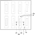
- the semiconductor device is an RC (ie, ReverseReConducting) -IGBT in which an IGBT region 1 having an IGBT element 1a and an FWD region 2 having an FWD element 2a are formed in the same chip. .
- RC ReverseReConducting
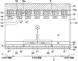
- the semiconductor device has a semiconductor substrate 10 that constitutes an N ⁇ type drift layer 11.
- the semiconductor substrate 10 is formed of a silicon substrate.
- a P-type base layer 12 is formed on the drift layer 11 (that is, on the one surface 10a side of the semiconductor substrate 10).
- the base layer 12 is formed, for example, by performing heat treatment after P-type impurities are ion-implanted from the one surface 10 a side of the semiconductor substrate 10.
- a plurality of trenches 13 are formed in the semiconductor substrate 10 so as to penetrate the base layer 12 and reach the drift layer 11. Thereby, the base layer 12 is separated into a plurality by the trench 13.
- the plurality of trenches 13 are formed in the IGBT region 1 and the FWD region 2, respectively, along one direction of the planar direction of the one surface 10a of the semiconductor substrate 10 (that is, the direction perpendicular to the paper surface in FIG. 2). Are formed at regular intervals.
- an N + -type emitter region 14 having a higher impurity concentration than the drift layer 11 and a higher impurity concentration than the base layer 12 are provided.
- P + -type contact regions 15 are formed. Specifically, the emitter region 14 is formed to terminate in the base layer 12 and to be in contact with the side surface of the trench 13. Further, the contact region 15 is formed so as to terminate in the base layer 12, similarly to the emitter region 14.
- the emitter region 14 extends in a rod shape so as to be in contact with the side surface of the trench 13 along the longitudinal direction of the trench 13 in the region between the trenches 13, and terminates inside the tip of the trench 13.
- the contact region 15 is sandwiched between the two emitter regions 14 and extends in a rod shape along the longitudinal direction of the trench 13 (that is, the emitter region 14). Note that the contact region 15 of the present embodiment is formed deeper than the emitter region 14 with respect to the one surface 10a of the semiconductor substrate 10.
- Each trench 13 is buried with a gate insulating film 16 formed so as to cover the wall surface of each trench 13 and a gate electrode 17 made of polysilicon or the like formed on the gate insulating film 16. .
- a trench gate structure is configured.
- the portion of the wall surface of the trench 13 located between the emitter region 14 and the drift layer 11 corresponds to the surface of the base layer located between the emitter region and the drift layer.
- An interlayer insulating film 18 made of BPSG or the like is formed on one surface 10a of the semiconductor substrate 10.
- An upper electrode 19 is formed on the interlayer insulating film 18 to be electrically connected to the emitter region 14 and the contact region 15 (that is, the base layer 12) through a contact hole 18a formed in the interlayer insulating film 18.
- an upper electrode 19 that functions as an emitter electrode in the IGBT region 1 and functions as an anode electrode in the FWD region 2 is formed on the interlayer insulating film 18.
- the upper electrode 19 corresponds to the first electrode.
- an N-type field stop layer (hereinafter referred to as FS) having a higher impurity concentration than the drift layer 11 is provided. 20) is formed.
- a P + -type collector layer 21 is formed on the opposite side of the drift layer 11 across the FS layer 20, and in the FWD region 2, N on the opposite side of the drift layer 11 across the FS layer 20.
- a + -type cathode layer 22 is formed. That is, the collector layer 21 and the cathode layer 22 are formed adjacent to each other on the opposite side of the drift layer 11 with the FS layer 20 interposed therebetween.
- the IGBT region 1 and the FWD region 2 are partitioned depending on whether the layer formed on the other surface 10 b side of the semiconductor substrate 10 is the collector layer 21 or the cathode layer 22.
- the part on the collector layer 21 is the IGBT region 1 and the part on the cathode layer 22 is the FWD region 2.
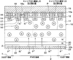
- the cathode layer 22 extends along one direction in the plane direction of the semiconductor substrate 10 (that is, the vertical direction on the paper surface in FIG. 1).
- the collector layer 21 and the cathode layer 22 are electrically connected to the side opposite to the drift layer 11 (that is, the other surface 10b of the semiconductor substrate 10) with the collector layer 21 and the cathode layer 22 interposed therebetween.
- a lower electrode 23 connected to is formed. That is, the lower electrode 23 that functions as a collector electrode in the IGBT region 1 and functions as a cathode electrode in the FWD region 2 is formed. In the present embodiment, the lower electrode 23 corresponds to the second electrode.
- the FWD element 2 is a PN junction in which the base layer 12 and the contact region 15 are the anodes, and the drift layer 11, the FS layer 20, and the cathode layer 22 are the cathodes. 2a is configured.
- the cathode layer 22 is electrically connected to the lower electrode 23 and forms a PN junction with the FS layer 20.
- a P + type carrier injection layer 24 is formed at a position away from the collector layer 21. .
- the carrier injection layer 24 extends along the extending direction of the cathode layer 22 and includes the center in the width direction of the cathode layer 22. It is formed so as to be symmetrical with respect to the center. More specifically, the carrier injection layer 24 is formed so that the center in the width direction of the carrier injection layer 24 coincides with the center in the width direction of the cathode layer 22.
- the width direction of the cathode layer 22 is a direction parallel to the planar direction of the semiconductor substrate 10 and is a direction perpendicular to the extending direction of the cathode layer 22 (that is, the left-right direction in FIG. 2). That is.
- the width direction of the carrier injection layer 24 is a direction parallel to the planar direction of the semiconductor substrate 10 and a direction orthogonal to the extending direction of the carrier injection layer 24 (that is, the left-right direction in FIG. 2). ).
- the N type, N + type, and N ⁇ type correspond to the first conductivity type
- the P type and P + type correspond to the second conductivity type.
- the PN junction formed between the base layer 12 and the drift layer 11 is in a reverse conduction state, and a depletion layer is formed.
- a low level (for example, 0 V) voltage lower than the threshold voltage Vth of the insulated gate structure is applied to the gate electrode 17, no current flows between the upper electrode 19 and the lower electrode 23.
- a high level voltage equal to or higher than the threshold voltage Vth of the insulated gate structure is applied to the gate electrode 17 while a voltage higher than that of the upper electrode 19 is applied to the lower electrode 23.
- an inversion layer is formed in a portion of the base layer 12 that is in contact with the trench 13 where the gate electrode 17 is disposed.
- electrons are supplied from the emitter region 14 to the drift layer 11 through the inversion layer, whereby holes are supplied from the collector layer 21 to the drift layer 11, and the resistance of the drift layer 11 is controlled by conductivity modulation. When the value decreases, it is turned on.
- the IGBT element 1a is turned off and the FWD element 2a is turned on (that is, the FWD element 2a is diode-operated)
- the voltage applied to the upper electrode 19 and the lower electrode 23 is switched, and the upper electrode A voltage higher than that of the lower electrode 23 is applied to 19.
- a low level voltage eg, 0 V
- the inversion layer is not formed in the portion of the base layer 12 in contact with the trench 13, and holes are supplied from the base layer 12 and electrons are supplied from the cathode layer 22, whereby the FWD element 2 a operates as a diode. do.
- a reverse voltage is applied to the lower electrode 23 to apply a voltage higher than that of the upper electrode 19. That is, when the current is cut off from a state in which a forward current is flowing in the FWD element 2a, reverse voltage application is performed to apply a voltage higher than that of the upper electrode 19 to the lower electrode 23. As a result, the FWD element 2a enters a recovery state. In other words, holes in the base layer 12 are attracted to the upper electrode 19 side, and electrons in the drift layer 11 are attracted to the lower electrode 23 side, whereby a recovery current is generated. The depletion layer grows.
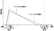
- the voltage between the PN junctions composed of the carrier injection layer 24 and the FS layer 20 acts as a potential barrier as described above. It is necessary to exceed. That is, if the width of the carrier injection layer 24 is too short, the potential of the FS layer 20 on the carrier injection layer 24 does not drop sufficiently, and the voltage between the PN junctions constituted by the carrier injection layer 24 and the FS layer 20 is reduced. Does not rise enough.
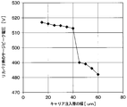
- the surge peak voltage during recovery is high when the width of the carrier injection layer 24 is less than 40 ⁇ m, but sharply decreases when the width of the carrier injection layer 24 is 40 ⁇ m or more. This is because when the width of the carrier injection layer 24 is less than 40 ⁇ m, the voltage between the PN junctions constituted by the carrier injection layer 24 and the FS layer 20 does not sufficiently increase during recovery, and the carrier injection layer 24 This is because holes are not injected from the surface.
- the surge peak voltage during recovery is low because the voltage between the PN junctions composed of the carrier injection layer 24 and the FS layer 20 is sufficiently increased during recovery. This is because holes are injected from the carrier injection layer 24.
- the impurity concentration of the FS layer 20 is set to 3.0 ⁇ 10 16 cm ⁇ 3
- the width of the cathode layer 22 (that is, the width of the FWD region 2) is constant
- FIG. 6 when the width of the carrier injection layer 24 is 20 ⁇ m to 40 ⁇ m, and when the width is 45 ⁇ m to 60 ⁇ m, the surge peak voltage at the time of recovery gradually increases as the width of the carrier injection layer 24 increases. This is because the remaining width of the cathode layer 22 is relatively changed by changing the width of the carrier injection layer 24. That is, this is because the total amount of electrons supplied from the cathode layer 22 to the drift layer 11 changes when the FWD element 2a is in the on state.
- the impurity concentration of the FS layer 20 is too high on the carrier injection layer 24.
- the potential of the FS layer 20 does not drop sufficiently. That is, even if the resistance value of the FS layer 20 is too low, the potential of the FS layer 20 on the carrier injection layer 24 does not drop sufficiently.
- FIG. 7 shows a simulation result of the 800 V withstand voltage band semiconductor device in which the thickness of the semiconductor substrate 10 is 75 to 85 ⁇ m and the specific resistance is 40 to 50 ⁇ ⁇ m.
- the necessary minimum width of the carrier injection layer 24 in FIG. 7 is that the voltage between the PN junctions composed of the carrier injection layer 24 and the FS layer 20 exceeds the potential barrier (that is, about 0.7 V). This is the minimum width of the necessary carrier injection layer 24.
- the impurity concentration of the FS layer 20 and the required minimum width of the carrier injection layer 24 are proportional to each other, and the required minimum width of the carrier injection layer 24 increases as the impurity concentration of the FS layer 20 increases. .
- the present inventors satisfy the following equation, assuming that the impurity concentration of the FS layer 20 is Nfs [cm ⁇ 3 ] and the necessary minimum width of the carrier injection layer 24 is W [ ⁇ m]. During the recovery, it has been found that the voltage between the PN junctions constituted by the carrier injection layer 24 and the FS layer 20 becomes equal to or higher than the potential barrier.
- the carrier injection layer 24 is formed in the cathode layer 22, and holes are injected from the carrier injection layer 24 into the drift layer 11 during recovery. For this reason, at the time of recovery, it is possible to suppress the depletion layer formed between the base layer 12 and the drift layer 11 from extending toward the other surface 10b side of the semiconductor substrate 10 and to reduce the surge peak voltage at the time of recovery. .
- the thickness of the semiconductor substrate 10 can be reduced in order to reduce the loss.
- the carrier injection layer 24 of the present embodiment is applied to a semiconductor device in which the width of the IGBT element 1a is increased in order to suppress the snapback phenomenon in the IGBT element 1a and the width of the FWD element 2a is increased accordingly. You can also According to this, the surge peak voltage at the time of recovery can be reduced while suppressing the snapback phenomenon.
- the carrier injection layer 24 is arranged so as to include the center in the width direction of the cathode layer 22. That is, the carrier injection layer 24 is disposed at a position where the electron density is most likely to be the highest during recovery. For this reason, the density of electrons passing through the FS layer 20 on the carrier injection layer 24 is increased. Therefore, the potential of the FS layer 20 is sufficiently lowered, the voltage between the PN junction composed of the carrier injection layer 24 and the FS layer 20 is sufficiently increased, and holes are injected from the carrier injection layer 24 into the drift layer 11. Can be made easier.
- the carrier injection layer 24 and the FS layer 20 are configured to satisfy the above mathematical formula 1. For this reason, at the time of recovery, it is possible to suppress the occurrence of a problem that holes are not injected from the carrier injection layer 24 into the drift layer 11 and the surge peak voltage at the time of recovery is not reduced.
- each carrier injection layer 24 needs to be 40 ⁇ m or more.
- the width of one carrier injection layer 24 is 90 ⁇ m, the effect of reducing the width of 50 ⁇ m can be obtained.
- each of the two carrier injection layers 24 is set to 45 ⁇ m so as to have a width of 90 ⁇ m as a whole, Only a reduction effect of 5 ⁇ m width can be obtained. Also, when two carrier injection layers 24 are arranged, if the two widths are set to 65 ⁇ m so that each carrier injection layer 24 can obtain a reduction effect of 25 ⁇ m (that is, 50 ⁇ m as a whole), carrier injection is performed. The entire width of the layer 24 is 130 ⁇ m. In this case, when the FWD element 2a is in the ON state, electrons injected from the cathode layer 22 are reduced, and the ON voltage of the FWD element 2a is increased. Therefore, by disposing only one carrier injection layer 24 as in the present embodiment, it is possible to suppress an increase in the ON voltage of the FWD element 2a while reducing the magnitude of the surge peak voltage during recovery.
- the first conductivity type is N type and the second conductivity type is P type has been described.
- the first conductivity type is P type
- the second conductivity type is N type.
- a planar semiconductor device in which the gate electrode 17 is disposed on the one surface 10a of the semiconductor substrate 10 may be used instead of the trench gate type semiconductor device.
- the carrier injection layer 24 may not be formed so as to include the center of the width of the cathode layer 22. Even in such a semiconductor device, if holes are injected from the carrier injection layer 24 into the drift layer 11 during recovery, the same effect as in the first embodiment can be obtained. In addition, when the center in the width direction of the carrier injection layer 24 and the center in the width direction of the cathode layer 22 are deviated, the density of electrons passing through the FS layer 20 on the carrier injection layer 24 decreases. The necessary minimum width of the carrier injection layer 24 is translated in the upward direction (that is, the direction in which the carrier injection layer 24 becomes longer).
- a plurality of carrier injection layers 24 may be formed.
Landscapes
- Metal-Oxide And Bipolar Metal-Oxide Semiconductor Integrated Circuits (AREA)
Priority Applications (2)
| Application Number | Priority Date | Filing Date | Title |
|---|---|---|---|
| CN201780029794.6A CN109155334B (zh) | 2016-05-17 | 2017-04-20 | 半导体装置 |
| US16/188,533 US11217580B2 (en) | 2016-05-17 | 2018-11-13 | Semiconductor device including insulated gate bipolar transistor element and freewheeling diode element |
Applications Claiming Priority (2)
| Application Number | Priority Date | Filing Date | Title |
|---|---|---|---|
| JP2016098875A JP2017208413A (ja) | 2016-05-17 | 2016-05-17 | 半導体装置 |
| JP2016-098875 | 2016-05-17 |
Related Child Applications (1)
| Application Number | Title | Priority Date | Filing Date |
|---|---|---|---|
| US16/188,533 Continuation US11217580B2 (en) | 2016-05-17 | 2018-11-13 | Semiconductor device including insulated gate bipolar transistor element and freewheeling diode element |
Publications (1)
| Publication Number | Publication Date |
|---|---|
| WO2017199679A1 true WO2017199679A1 (ja) | 2017-11-23 |
Family
ID=60325161
Family Applications (1)
| Application Number | Title | Priority Date | Filing Date |
|---|---|---|---|
| PCT/JP2017/015874 Ceased WO2017199679A1 (ja) | 2016-05-17 | 2017-04-20 | 半導体装置 |
Country Status (4)
| Country | Link |
|---|---|
| US (1) | US11217580B2 (enExample) |
| JP (1) | JP2017208413A (enExample) |
| CN (1) | CN109155334B (enExample) |
| WO (1) | WO2017199679A1 (enExample) |
Cited By (3)
| Publication number | Priority date | Publication date | Assignee | Title |
|---|---|---|---|---|
| CN110137249A (zh) * | 2018-02-09 | 2019-08-16 | 苏州东微半导体有限公司 | Igbt功率器件及其制造方法 |
| WO2020174799A1 (ja) * | 2019-02-27 | 2020-09-03 | 富士電機株式会社 | 半導体装置 |
| CN117650165A (zh) * | 2023-10-31 | 2024-03-05 | 海信家电集团股份有限公司 | 半导体装置 |
Families Citing this family (11)
| Publication number | Priority date | Publication date | Assignee | Title |
|---|---|---|---|---|
| JP6935731B2 (ja) | 2017-11-16 | 2021-09-15 | 株式会社デンソー | 半導体装置 |
| JP7010184B2 (ja) * | 2018-09-13 | 2022-01-26 | 株式会社デンソー | 半導体装置 |
| WO2020208995A1 (ja) * | 2019-04-08 | 2020-10-15 | 住友電気工業株式会社 | 半導体装置 |
| GB2584698B (en) * | 2019-06-12 | 2022-09-14 | Mqsemi Ag | Non-punch-through reverse-conducting power semiconductor device and method for producing same |
| CN110797403B (zh) * | 2019-10-18 | 2023-08-01 | 上海睿驱微电子科技有限公司 | 一种rc-igbt半导体装置 |
| CN110797404B (zh) * | 2019-10-18 | 2023-11-28 | 上海睿驱微电子科技有限公司 | 一种rc-igbt半导体器件 |
| DE102020123847B4 (de) * | 2020-09-14 | 2025-11-20 | Infineon Technologies Ag | Feldstoppgebiet enthaltende leistungs-halbleiterdiode und verfahren |
| JP7456902B2 (ja) | 2020-09-17 | 2024-03-27 | 株式会社東芝 | 半導体装置 |
| DE102021115971A1 (de) * | 2021-06-21 | 2022-12-22 | Infineon Technologies Ag | Feldstoppgebiet enthaltende halbleitervorrichtung |
| JP2024163409A (ja) * | 2023-05-12 | 2024-11-22 | ミネベアパワーデバイス株式会社 | 半導体装置 |
| CN116632053B (zh) * | 2023-07-25 | 2024-01-30 | 深圳市美浦森半导体有限公司 | 一种rc-igbt器件的控制方法 |
Citations (2)
| Publication number | Priority date | Publication date | Assignee | Title |
|---|---|---|---|---|
| JP2013021142A (ja) * | 2011-07-12 | 2013-01-31 | Toyota Central R&D Labs Inc | 半導体装置 |
| JP2014103376A (ja) * | 2012-09-24 | 2014-06-05 | Toshiba Corp | 半導体装置 |
Family Cites Families (9)
| Publication number | Priority date | Publication date | Assignee | Title |
|---|---|---|---|---|
| JP5157201B2 (ja) | 2006-03-22 | 2013-03-06 | 株式会社デンソー | 半導体装置 |
| JP5678469B2 (ja) | 2010-05-07 | 2015-03-04 | 株式会社デンソー | 半導体装置 |
| JP5582102B2 (ja) * | 2010-07-01 | 2014-09-03 | 株式会社デンソー | 半導体装置 |
| JP5321669B2 (ja) | 2010-11-25 | 2013-10-23 | 株式会社デンソー | 半導体装置 |
| JP2013080796A (ja) * | 2011-10-03 | 2013-05-02 | Toyota Central R&D Labs Inc | 半導体装置 |
| JP2013235891A (ja) | 2012-05-07 | 2013-11-21 | Denso Corp | 半導体装置 |
| JP5981859B2 (ja) | 2013-02-15 | 2016-08-31 | 株式会社豊田中央研究所 | ダイオード及びダイオードを内蔵する半導体装置 |
| JP6158123B2 (ja) * | 2014-03-14 | 2017-07-05 | 株式会社東芝 | 半導体装置 |
| JP6269860B2 (ja) * | 2014-12-17 | 2018-01-31 | 三菱電機株式会社 | 半導体装置 |
-
2016
- 2016-05-17 JP JP2016098875A patent/JP2017208413A/ja active Pending
-
2017
- 2017-04-20 CN CN201780029794.6A patent/CN109155334B/zh active Active
- 2017-04-20 WO PCT/JP2017/015874 patent/WO2017199679A1/ja not_active Ceased
-
2018
- 2018-11-13 US US16/188,533 patent/US11217580B2/en active Active
Patent Citations (2)
| Publication number | Priority date | Publication date | Assignee | Title |
|---|---|---|---|---|
| JP2013021142A (ja) * | 2011-07-12 | 2013-01-31 | Toyota Central R&D Labs Inc | 半導体装置 |
| JP2014103376A (ja) * | 2012-09-24 | 2014-06-05 | Toshiba Corp | 半導体装置 |
Cited By (9)
| Publication number | Priority date | Publication date | Assignee | Title |
|---|---|---|---|---|
| CN110137249A (zh) * | 2018-02-09 | 2019-08-16 | 苏州东微半导体有限公司 | Igbt功率器件及其制造方法 |
| US11450763B2 (en) | 2018-02-09 | 2022-09-20 | Suzhou Oriental Semiconductor Co., Ltd. | IGBT power device and fabrication method therefor |
| WO2020174799A1 (ja) * | 2019-02-27 | 2020-09-03 | 富士電機株式会社 | 半導体装置 |
| JPWO2020174799A1 (ja) * | 2019-02-27 | 2021-09-13 | 富士電機株式会社 | 半導体装置 |
| JP7156495B2 (ja) | 2019-02-27 | 2022-10-19 | 富士電機株式会社 | 半導体装置 |
| US11488951B2 (en) | 2019-02-27 | 2022-11-01 | Fuji Electric Co., Ltd. | Semiconductor device |
| US11810913B2 (en) | 2019-02-27 | 2023-11-07 | Fuji Electric Co., Ltd. | Semiconductor device |
| CN117650165A (zh) * | 2023-10-31 | 2024-03-05 | 海信家电集团股份有限公司 | 半导体装置 |
| CN117650165B (zh) * | 2023-10-31 | 2024-05-31 | 海信家电集团股份有限公司 | 半导体装置 |
Also Published As
| Publication number | Publication date |
|---|---|
| CN109155334B (zh) | 2021-11-05 |
| CN109155334A (zh) | 2019-01-04 |
| US11217580B2 (en) | 2022-01-04 |
| JP2017208413A (ja) | 2017-11-24 |
| US20190081163A1 (en) | 2019-03-14 |
Similar Documents
| Publication | Publication Date | Title |
|---|---|---|
| WO2017199679A1 (ja) | 半導体装置 | |
| JP6791312B2 (ja) | 半導体装置 | |
| CN109964317B (zh) | 半导体装置 | |
| JP6641983B2 (ja) | 半導体装置 | |
| JP5787853B2 (ja) | 電力用半導体装置 | |
| JP6443267B2 (ja) | 半導体装置 | |
| CN1967868B (zh) | 半导体装置及其制造方法 | |
| JP5206096B2 (ja) | ダイオードとそのダイオードを備えている半導体装置 | |
| WO2016009616A1 (ja) | 半導体装置 | |
| JP6996461B2 (ja) | 半導体装置 | |
| JP5537359B2 (ja) | 半導体装置 | |
| JP6954333B2 (ja) | 半導体装置 | |
| CN109509789A (zh) | 半导体装置 | |
| JP7172920B2 (ja) | 半導体装置 | |
| JP2017195224A (ja) | スイッチング素子 | |
| WO2016114131A1 (ja) | 半導体装置 | |
| US11289476B2 (en) | Semiconductor device including carrier injection layers | |
| JP5151175B2 (ja) | 半導体装置 | |
| JP2016149429A (ja) | 逆導通igbt | |
| US7741655B2 (en) | Semiconductor device | |
| WO2018230312A1 (ja) | 半導体装置 | |
| JP2021019155A (ja) | 半導体装置 | |
| JP2021040070A (ja) | 半導体装置 | |
| JP2002231931A (ja) | 半導体装置 |
Legal Events
| Date | Code | Title | Description |
|---|---|---|---|
| NENP | Non-entry into the national phase |
Ref country code: DE |
|
| 121 | Ep: the epo has been informed by wipo that ep was designated in this application |
Ref document number: 17799110 Country of ref document: EP Kind code of ref document: A1 |
|
| 122 | Ep: pct application non-entry in european phase |
Ref document number: 17799110 Country of ref document: EP Kind code of ref document: A1 |