JP7010184B2 - 半導体装置 - Google Patents
半導体装置 Download PDFInfo
- Publication number
- JP7010184B2 JP7010184B2 JP2018171732A JP2018171732A JP7010184B2 JP 7010184 B2 JP7010184 B2 JP 7010184B2 JP 2018171732 A JP2018171732 A JP 2018171732A JP 2018171732 A JP2018171732 A JP 2018171732A JP 7010184 B2 JP7010184 B2 JP 7010184B2
- Authority
- JP
- Japan
- Prior art keywords
- layer
- collector
- semiconductor device
- carrier concentration
- collector layer
- Prior art date
- Legal status (The legal status is an assumption and is not a legal conclusion. Google has not performed a legal analysis and makes no representation as to the accuracy of the status listed.)
- Active
Links
- 239000004065 semiconductor Substances 0.000 title claims description 84
- 239000010410 layer Substances 0.000 claims description 290
- 239000012535 impurity Substances 0.000 claims description 18
- 239000002344 surface layer Substances 0.000 claims description 4
- 230000005684 electric field Effects 0.000 description 48
- 239000000758 substrate Substances 0.000 description 21
- 238000009826 distribution Methods 0.000 description 7
- 238000004088 simulation Methods 0.000 description 7
- 210000000746 body region Anatomy 0.000 description 6
- 230000007423 decrease Effects 0.000 description 6
- 230000015556 catabolic process Effects 0.000 description 3
- 239000011229 interlayer Substances 0.000 description 3
- 230000004048 modification Effects 0.000 description 3
- 238000012986 modification Methods 0.000 description 3
- 239000005380 borophosphosilicate glass Substances 0.000 description 2
- 238000011156 evaluation Methods 0.000 description 2
- 238000004519 manufacturing process Methods 0.000 description 2
- 230000001133 acceleration Effects 0.000 description 1
- 230000003247 decreasing effect Effects 0.000 description 1
- 230000002950 deficient Effects 0.000 description 1
- 238000010586 diagram Methods 0.000 description 1
- 238000002347 injection Methods 0.000 description 1
- 239000007924 injection Substances 0.000 description 1
- 238000005468 ion implantation Methods 0.000 description 1
- 229910021420 polycrystalline silicon Inorganic materials 0.000 description 1
- 229920005591 polysilicon Polymers 0.000 description 1
Images


Classifications
-
- H—ELECTRICITY
- H01—ELECTRIC ELEMENTS
- H01L—SEMICONDUCTOR DEVICES NOT COVERED BY CLASS H10
- H01L29/00—Semiconductor devices adapted for rectifying, amplifying, oscillating or switching, or capacitors or resistors with at least one potential-jump barrier or surface barrier, e.g. PN junction depletion layer or carrier concentration layer; Details of semiconductor bodies or of electrodes thereof ; Multistep manufacturing processes therefor
- H01L29/02—Semiconductor bodies ; Multistep manufacturing processes therefor
- H01L29/06—Semiconductor bodies ; Multistep manufacturing processes therefor characterised by their shape; characterised by the shapes, relative sizes, or dispositions of the semiconductor regions ; characterised by the concentration or distribution of impurities within semiconductor regions
- H01L29/0603—Semiconductor bodies ; Multistep manufacturing processes therefor characterised by their shape; characterised by the shapes, relative sizes, or dispositions of the semiconductor regions ; characterised by the concentration or distribution of impurities within semiconductor regions characterised by particular constructional design considerations, e.g. for preventing surface leakage, for controlling electric field concentration or for internal isolations regions
- H01L29/0607—Semiconductor bodies ; Multistep manufacturing processes therefor characterised by their shape; characterised by the shapes, relative sizes, or dispositions of the semiconductor regions ; characterised by the concentration or distribution of impurities within semiconductor regions characterised by particular constructional design considerations, e.g. for preventing surface leakage, for controlling electric field concentration or for internal isolations regions for preventing surface leakage or controlling electric field concentration
- H01L29/0638—Semiconductor bodies ; Multistep manufacturing processes therefor characterised by their shape; characterised by the shapes, relative sizes, or dispositions of the semiconductor regions ; characterised by the concentration or distribution of impurities within semiconductor regions characterised by particular constructional design considerations, e.g. for preventing surface leakage, for controlling electric field concentration or for internal isolations regions for preventing surface leakage or controlling electric field concentration for preventing surface leakage due to surface inversion layer, e.g. with channel stopper
-
- H—ELECTRICITY
- H01—ELECTRIC ELEMENTS
- H01L—SEMICONDUCTOR DEVICES NOT COVERED BY CLASS H10
- H01L29/00—Semiconductor devices adapted for rectifying, amplifying, oscillating or switching, or capacitors or resistors with at least one potential-jump barrier or surface barrier, e.g. PN junction depletion layer or carrier concentration layer; Details of semiconductor bodies or of electrodes thereof ; Multistep manufacturing processes therefor
- H01L29/02—Semiconductor bodies ; Multistep manufacturing processes therefor
- H01L29/36—Semiconductor bodies ; Multistep manufacturing processes therefor characterised by the concentration or distribution of impurities in the bulk material
-
- H—ELECTRICITY
- H01—ELECTRIC ELEMENTS
- H01L—SEMICONDUCTOR DEVICES NOT COVERED BY CLASS H10
- H01L29/00—Semiconductor devices adapted for rectifying, amplifying, oscillating or switching, or capacitors or resistors with at least one potential-jump barrier or surface barrier, e.g. PN junction depletion layer or carrier concentration layer; Details of semiconductor bodies or of electrodes thereof ; Multistep manufacturing processes therefor
- H01L29/66—Types of semiconductor device ; Multistep manufacturing processes therefor
- H01L29/68—Types of semiconductor device ; Multistep manufacturing processes therefor controllable by only the electric current supplied, or only the electric potential applied, to an electrode which does not carry the current to be rectified, amplified or switched
- H01L29/70—Bipolar devices
- H01L29/72—Transistor-type devices, i.e. able to continuously respond to applied control signals
- H01L29/739—Transistor-type devices, i.e. able to continuously respond to applied control signals controlled by field-effect, e.g. bipolar static induction transistors [BSIT]
- H01L29/7393—Insulated gate bipolar mode transistors, i.e. IGBT; IGT; COMFET
- H01L29/7395—Vertical transistors, e.g. vertical IGBT
- H01L29/7396—Vertical transistors, e.g. vertical IGBT with a non planar surface, e.g. with a non planar gate or with a trench or recess or pillar in the surface of the emitter, base or collector region for improving current density or short circuiting the emitter and base regions
- H01L29/7397—Vertical transistors, e.g. vertical IGBT with a non planar surface, e.g. with a non planar gate or with a trench or recess or pillar in the surface of the emitter, base or collector region for improving current density or short circuiting the emitter and base regions and a gate structure lying on a slanted or vertical surface or formed in a groove, e.g. trench gate IGBT
-
- H—ELECTRICITY
- H01—ELECTRIC ELEMENTS
- H01L—SEMICONDUCTOR DEVICES NOT COVERED BY CLASS H10
- H01L29/00—Semiconductor devices adapted for rectifying, amplifying, oscillating or switching, or capacitors or resistors with at least one potential-jump barrier or surface barrier, e.g. PN junction depletion layer or carrier concentration layer; Details of semiconductor bodies or of electrodes thereof ; Multistep manufacturing processes therefor
- H01L29/66—Types of semiconductor device ; Multistep manufacturing processes therefor
- H01L29/68—Types of semiconductor device ; Multistep manufacturing processes therefor controllable by only the electric current supplied, or only the electric potential applied, to an electrode which does not carry the current to be rectified, amplified or switched
- H01L29/76—Unipolar devices, e.g. field effect transistors
- H01L29/772—Field effect transistors
- H01L29/78—Field effect transistors with field effect produced by an insulated gate
Landscapes
- Engineering & Computer Science (AREA)
- Microelectronics & Electronic Packaging (AREA)
- Power Engineering (AREA)
- Physics & Mathematics (AREA)
- Ceramic Engineering (AREA)
- Condensed Matter Physics & Semiconductors (AREA)
- General Physics & Mathematics (AREA)
- Computer Hardware Design (AREA)
- Electrodes Of Semiconductors (AREA)
Description
第1実施形態の半導体装置について図1を参照しつつ説明する。なお、本実施形態の半導体装置1は、例えば、インバータ、DC/DCコンバータ等の電源回路に使用されるパワースイッチング素子として利用されると好適である。
第2実施形態について説明する。第2実施形態は、第1実施形態に対し、コレクタ層21におけるキャリア濃度の分布を変更したものである。その他に関しては、第1実施形態と同様であるため、ここでは説明を省略する。
第3実施形態について説明する。第3実施形態は、第1実施形態に対し、FS層20におけるキャリア濃度の分布を変更したものである。その他に関しては、第1実施形態と同様であるため、ここでは説明を省略する。
第4実施形態について説明する。第4実施形態は、第1実施形態に対し、FS層20におけるキャリア濃度の分布を変更したものである。その他に関しては、第1実施形態と同様であるため、ここでは説明を省略する。
本発明は上記した実施形態に限定されるものではなく、特許請求の範囲に記載した範囲内において適宜変更が可能である。
11 ドリフト層
12 ベース層
14 ゲート絶縁膜
15 ゲート電極
16 エミッタ領域
19 第1電極
22 第2電極
Claims (4)
- フィールドストップ層(20)を有する半導体装置であって、
第1導電型のドリフト層(11)と、
前記ドリフト層上に形成された第2導電型のベース層(12)と、
前記ベース層の表層部に形成された第1導電型のエミッタ領域(16)と、
前記ベース層のうちの前記ドリフト層と前記エミッタ領域との間に形成されたゲート絶縁膜(14)と、
前記ゲート絶縁膜上に形成されたゲート電極(15)と、
前記ドリフト層のうちの前記ベース層側と反対側に形成された第2導電型のコレクタ層(21)と、
前記コレクタ層と前記ドリフト層との間に形成され、前記ドリフト層よりも高キャリア濃度とされた第1導電型の前記フィールドストップ層と、
前記ベース層および前記エミッタ領域と電気的に接続される第1電極(19)と、
前記コレクタ層と電気的に接続される第2電極(22)と、を備え、
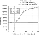
前記フィールドストップ層および前記コレクタ層は、前記フィールドストップ層におけるキャリア濃度が最大となる最大ピーク位置と前記コレクタ層におけるキャリア濃度が最大となる最大ピーク位置との間の距離をX[μm]、前記フィールドストップ層を構成するドーズ量に対する前記コレクタ層を構成するドーズ量の比である不純物総量比をYとすると、Y≧0.69X2+0.08X+0.86を満たす構成とされており、
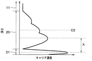
前記コレクタ層は、前記コレクタ層と前記フィールドストップ層との積層方向において、前記コレクタ層の最大ピーク位置が当該コレクタ層の中心(C1)より前記ドリフト層側に位置している半導体装置。 - 前記コレクタ層は、前記キャリア濃度が複数のピークを有するように構成され、前記中心より前記ドリフト層側と反対側に、前記キャリア濃度が最大となる最大ピークよりも小さい補助ピークを有している請求項1に記載の半導体装置。
- 前記フィールドストップ層は、前記コレクタ層と前記フィールドストップ層との積層方向において、前記フィールドストップ層におけるキャリア濃度が最大となる最大ピーク位置が当該フィールドストップ層の中心(C2)より前記ドリフト層側に位置している請求項1または2に記載の半導体装置。
- 前記フィールドストップ層は、前記コレクタ層と前記フィールドストップ層との積層方向において、前記フィールドストップ層におけるキャリア濃度が最大となる最大ピーク位置が当該フィールドストップ層の中心(C2)より前記コレクタ層側に位置している請求項1または2に記載の半導体装置。
Priority Applications (4)
| Application Number | Priority Date | Filing Date | Title |
|---|---|---|---|
| JP2018171732A JP7010184B2 (ja) | 2018-09-13 | 2018-09-13 | 半導体装置 |
| CN201980059059.9A CN112689902A (zh) | 2018-09-13 | 2019-08-29 | 半导体装置 |
| PCT/JP2019/033934 WO2020054446A1 (ja) | 2018-09-13 | 2019-08-29 | 半導体装置 |
| US17/198,807 US20210217845A1 (en) | 2018-09-13 | 2021-03-11 | Semiconductor device |
Applications Claiming Priority (1)
| Application Number | Priority Date | Filing Date | Title |
|---|---|---|---|
| JP2018171732A JP7010184B2 (ja) | 2018-09-13 | 2018-09-13 | 半導体装置 |
Publications (3)
| Publication Number | Publication Date |
|---|---|
| JP2020043301A JP2020043301A (ja) | 2020-03-19 |
| JP2020043301A5 JP2020043301A5 (ja) | 2021-01-28 |
| JP7010184B2 true JP7010184B2 (ja) | 2022-01-26 |
Family
ID=69778270
Family Applications (1)
| Application Number | Title | Priority Date | Filing Date |
|---|---|---|---|
| JP2018171732A Active JP7010184B2 (ja) | 2018-09-13 | 2018-09-13 | 半導体装置 |
Country Status (4)
| Country | Link |
|---|---|
| US (1) | US20210217845A1 (ja) |
| JP (1) | JP7010184B2 (ja) |
| CN (1) | CN112689902A (ja) |
| WO (1) | WO2020054446A1 (ja) |
Families Citing this family (1)
| Publication number | Priority date | Publication date | Assignee | Title |
|---|---|---|---|---|
| WO2024090117A1 (ja) * | 2022-10-27 | 2024-05-02 | 株式会社デンソー | 半導体装置 |
Citations (3)
| Publication number | Priority date | Publication date | Assignee | Title |
|---|---|---|---|---|
| US20080001257A1 (en) | 2006-06-30 | 2008-01-03 | Infineon Technologies Austria Ag | Semiconductor device with a field stop zone |
| JP2012156207A (ja) | 2011-01-24 | 2012-08-16 | Mitsubishi Electric Corp | 半導体装置と半導体装置の製造方法 |
| WO2016204126A1 (ja) | 2015-06-17 | 2016-12-22 | 富士電機株式会社 | 半導体装置 |
Family Cites Families (9)
| Publication number | Priority date | Publication date | Assignee | Title |
|---|---|---|---|---|
| JP2011166034A (ja) * | 2010-02-12 | 2011-08-25 | Fuji Electric Co Ltd | 半導体装置の製造方法 |
| CN104157685B (zh) * | 2010-07-27 | 2018-01-16 | 株式会社电装 | 具有开关元件和续流二极管的半导体装置及其控制方法 |
| JP2012204636A (ja) * | 2011-03-25 | 2012-10-22 | Toshiba Corp | 半導体装置およびその製造方法 |
| CN106128946B (zh) * | 2011-05-18 | 2019-03-08 | 富士电机株式会社 | 半导体装置及半导体装置的制造方法 |
| JP2013235891A (ja) * | 2012-05-07 | 2013-11-21 | Denso Corp | 半導体装置 |
| JP6277814B2 (ja) * | 2014-03-25 | 2018-02-14 | 株式会社デンソー | 半導体装置 |
| JP6720569B2 (ja) * | 2015-02-25 | 2020-07-08 | 株式会社デンソー | 半導体装置 |
| JP6443267B2 (ja) * | 2015-08-28 | 2018-12-26 | 株式会社デンソー | 半導体装置 |
| JP2017208413A (ja) * | 2016-05-17 | 2017-11-24 | 株式会社デンソー | 半導体装置 |
-
2018
- 2018-09-13 JP JP2018171732A patent/JP7010184B2/ja active Active
-
2019
- 2019-08-29 CN CN201980059059.9A patent/CN112689902A/zh active Pending
- 2019-08-29 WO PCT/JP2019/033934 patent/WO2020054446A1/ja active Application Filing
-
2021
- 2021-03-11 US US17/198,807 patent/US20210217845A1/en active Pending
Patent Citations (3)
| Publication number | Priority date | Publication date | Assignee | Title |
|---|---|---|---|---|
| US20080001257A1 (en) | 2006-06-30 | 2008-01-03 | Infineon Technologies Austria Ag | Semiconductor device with a field stop zone |
| JP2012156207A (ja) | 2011-01-24 | 2012-08-16 | Mitsubishi Electric Corp | 半導体装置と半導体装置の製造方法 |
| WO2016204126A1 (ja) | 2015-06-17 | 2016-12-22 | 富士電機株式会社 | 半導体装置 |
Also Published As
| Publication number | Publication date |
|---|---|
| US20210217845A1 (en) | 2021-07-15 |
| JP2020043301A (ja) | 2020-03-19 |
| CN112689902A (zh) | 2021-04-20 |
| WO2020054446A1 (ja) | 2020-03-19 |
Similar Documents
| Publication | Publication Date | Title |
|---|---|---|
| US9105680B2 (en) | Insulated gate bipolar transistor | |
| US9153676B2 (en) | Insulated gate bipolar transistor | |
| US8975690B2 (en) | Semiconductor device | |
| JP5865618B2 (ja) | 半導体装置 | |
| TWI575736B (zh) | 雙溝槽閘極絕緣閘雙極電晶體結構 | |
| JP6356803B2 (ja) | 絶縁ゲートバイポーラトランジスタ | |
| KR101701667B1 (ko) | 트렌치 게이트 전극을 이용하는 igbt | |
| US11075285B2 (en) | Insulated gate power semiconductor device and method for manufacturing such a device | |
| JP6571467B2 (ja) | 絶縁ゲート型スイッチング素子とその製造方法 | |
| JP5200373B2 (ja) | 半導体装置 | |
| CN108365007B (zh) | 绝缘栅双极型晶体管 | |
| JPWO2016042955A1 (ja) | 半導体装置および半導体装置の製造方法 | |
| JP2006332591A (ja) | 半導体装置 | |
| US11264475B2 (en) | Semiconductor device having a gate electrode formed in a trench structure | |
| JP2017191817A (ja) | スイッチング素子の製造方法 | |
| JP5838176B2 (ja) | 半導体装置 | |
| JP7010184B2 (ja) | 半導体装置 | |
| JP2019117867A (ja) | 半導体装置 | |
| KR20150061201A (ko) | 전력 반도체 소자 및 그 제조 방법 | |
| CN108305893B (zh) | 半导体装置 | |
| US20150171198A1 (en) | Power semiconductor device | |
| WO2021220965A1 (ja) | 半導体装置 | |
| US20150144993A1 (en) | Power semiconductor device | |
| JP2017045874A (ja) | 半導体装置 | |
| JP2018125326A (ja) | 半導体装置 |
Legal Events
| Date | Code | Title | Description |
|---|---|---|---|
| A711 | Notification of change in applicant |
Free format text: JAPANESE INTERMEDIATE CODE: A711 Effective date: 20201030 |
|
| A521 | Request for written amendment filed |
Free format text: JAPANESE INTERMEDIATE CODE: A821 Effective date: 20201030 |
|
| A521 | Request for written amendment filed |
Free format text: JAPANESE INTERMEDIATE CODE: A523 Effective date: 20201209 |
|
| A621 | Written request for application examination |
Free format text: JAPANESE INTERMEDIATE CODE: A621 Effective date: 20210217 |
|
| TRDD | Decision of grant or rejection written | ||
| A01 | Written decision to grant a patent or to grant a registration (utility model) |
Free format text: JAPANESE INTERMEDIATE CODE: A01 Effective date: 20211214 |
|
| A61 | First payment of annual fees (during grant procedure) |
Free format text: JAPANESE INTERMEDIATE CODE: A61 Effective date: 20211227 |