JP2012204636A - 半導体装置およびその製造方法 - Google Patents
半導体装置およびその製造方法 Download PDFInfo
- Publication number
- JP2012204636A JP2012204636A JP2011068275A JP2011068275A JP2012204636A JP 2012204636 A JP2012204636 A JP 2012204636A JP 2011068275 A JP2011068275 A JP 2011068275A JP 2011068275 A JP2011068275 A JP 2011068275A JP 2012204636 A JP2012204636 A JP 2012204636A
- Authority
- JP
- Japan
- Prior art keywords
- layer
- conductivity type
- impurity concentration
- drift layer
- base layer
- Prior art date
- Legal status (The legal status is an assumption and is not a legal conclusion. Google has not performed a legal analysis and makes no representation as to the accuracy of the status listed.)
- Pending
Links
- 239000004065 semiconductor Substances 0.000 title claims abstract description 72
- 238000004519 manufacturing process Methods 0.000 title claims abstract description 11
- 239000012535 impurity Substances 0.000 claims abstract description 130
- 230000000149 penetrating effect Effects 0.000 abstract description 2
- 238000009413 insulation Methods 0.000 abstract 2
- 239000010410 layer Substances 0.000 description 237
- 238000010586 diagram Methods 0.000 description 12
- 230000007423 decrease Effects 0.000 description 9
- 238000000034 method Methods 0.000 description 8
- 230000015556 catabolic process Effects 0.000 description 6
- 239000000969 carrier Substances 0.000 description 5
- XUIMIQQOPSSXEZ-UHFFFAOYSA-N Silicon Chemical compound [Si] XUIMIQQOPSSXEZ-UHFFFAOYSA-N 0.000 description 4
- 239000013078 crystal Substances 0.000 description 4
- 229910052710 silicon Inorganic materials 0.000 description 4
- 239000010703 silicon Substances 0.000 description 4
- 238000005229 chemical vapour deposition Methods 0.000 description 3
- 238000005468 ion implantation Methods 0.000 description 3
- 238000012986 modification Methods 0.000 description 3
- 230000004048 modification Effects 0.000 description 3
- 229910052785 arsenic Inorganic materials 0.000 description 2
- RQNWIZPPADIBDY-UHFFFAOYSA-N arsenic atom Chemical compound [As] RQNWIZPPADIBDY-UHFFFAOYSA-N 0.000 description 2
- 230000005684 electric field Effects 0.000 description 2
- 238000005530 etching Methods 0.000 description 2
- 239000000463 material Substances 0.000 description 2
- 230000003647 oxidation Effects 0.000 description 2
- 238000007254 oxidation reaction Methods 0.000 description 2
- 238000001020 plasma etching Methods 0.000 description 2
- 229910021420 polycrystalline silicon Inorganic materials 0.000 description 2
- 238000004088 simulation Methods 0.000 description 2
- ZOXJGFHDIHLPTG-UHFFFAOYSA-N Boron Chemical compound [B] ZOXJGFHDIHLPTG-UHFFFAOYSA-N 0.000 description 1
- OAICVXFJPJFONN-UHFFFAOYSA-N Phosphorus Chemical compound [P] OAICVXFJPJFONN-UHFFFAOYSA-N 0.000 description 1
- 229910004298 SiO 2 Inorganic materials 0.000 description 1
- VYPSYNLAJGMNEJ-UHFFFAOYSA-N Silicium dioxide Chemical compound O=[Si]=O VYPSYNLAJGMNEJ-UHFFFAOYSA-N 0.000 description 1
- 230000001133 acceleration Effects 0.000 description 1
- 229910052796 boron Inorganic materials 0.000 description 1
- 238000009792 diffusion process Methods 0.000 description 1
- 230000000694 effects Effects 0.000 description 1
- 238000000605 extraction Methods 0.000 description 1
- 230000005669 field effect Effects 0.000 description 1
- 239000011229 interlayer Substances 0.000 description 1
- 229910044991 metal oxide Inorganic materials 0.000 description 1
- 150000004706 metal oxides Chemical class 0.000 description 1
- 229910052698 phosphorus Inorganic materials 0.000 description 1
- 239000011574 phosphorus Substances 0.000 description 1
- 229920005591 polysilicon Polymers 0.000 description 1
- 229920006395 saturated elastomer Polymers 0.000 description 1
- 229910052814 silicon oxide Inorganic materials 0.000 description 1
- 239000000126 substance Substances 0.000 description 1
Images


Classifications
-
- H—ELECTRICITY
- H01—ELECTRIC ELEMENTS
- H01L—SEMICONDUCTOR DEVICES NOT COVERED BY CLASS H10
- H01L29/00—Semiconductor devices adapted for rectifying, amplifying, oscillating or switching, or capacitors or resistors with at least one potential-jump barrier or surface barrier, e.g. PN junction depletion layer or carrier concentration layer; Details of semiconductor bodies or of electrodes thereof ; Multistep manufacturing processes therefor
- H01L29/66—Types of semiconductor device ; Multistep manufacturing processes therefor
- H01L29/68—Types of semiconductor device ; Multistep manufacturing processes therefor controllable by only the electric current supplied, or only the electric potential applied, to an electrode which does not carry the current to be rectified, amplified or switched
- H01L29/76—Unipolar devices, e.g. field effect transistors
- H01L29/772—Field effect transistors
- H01L29/78—Field effect transistors with field effect produced by an insulated gate
- H01L29/7801—DMOS transistors, i.e. MISFETs with a channel accommodating body or base region adjoining a drain drift region
- H01L29/7802—Vertical DMOS transistors, i.e. VDMOS transistors
- H01L29/7813—Vertical DMOS transistors, i.e. VDMOS transistors with trench gate electrode, e.g. UMOS transistors
-
- H—ELECTRICITY
- H01—ELECTRIC ELEMENTS
- H01L—SEMICONDUCTOR DEVICES NOT COVERED BY CLASS H10
- H01L29/00—Semiconductor devices adapted for rectifying, amplifying, oscillating or switching, or capacitors or resistors with at least one potential-jump barrier or surface barrier, e.g. PN junction depletion layer or carrier concentration layer; Details of semiconductor bodies or of electrodes thereof ; Multistep manufacturing processes therefor
- H01L29/02—Semiconductor bodies ; Multistep manufacturing processes therefor
- H01L29/06—Semiconductor bodies ; Multistep manufacturing processes therefor characterised by their shape; characterised by the shapes, relative sizes, or dispositions of the semiconductor regions ; characterised by the concentration or distribution of impurities within semiconductor regions
- H01L29/08—Semiconductor bodies ; Multistep manufacturing processes therefor characterised by their shape; characterised by the shapes, relative sizes, or dispositions of the semiconductor regions ; characterised by the concentration or distribution of impurities within semiconductor regions with semiconductor regions connected to an electrode carrying current to be rectified, amplified or switched and such electrode being part of a semiconductor device which comprises three or more electrodes
- H01L29/0843—Source or drain regions of field-effect devices
- H01L29/0847—Source or drain regions of field-effect devices of field-effect transistors with insulated gate
- H01L29/0852—Source or drain regions of field-effect devices of field-effect transistors with insulated gate of DMOS transistors
- H01L29/0873—Drain regions
- H01L29/0878—Impurity concentration or distribution
-
- H—ELECTRICITY
- H01—ELECTRIC ELEMENTS
- H01L—SEMICONDUCTOR DEVICES NOT COVERED BY CLASS H10
- H01L29/00—Semiconductor devices adapted for rectifying, amplifying, oscillating or switching, or capacitors or resistors with at least one potential-jump barrier or surface barrier, e.g. PN junction depletion layer or carrier concentration layer; Details of semiconductor bodies or of electrodes thereof ; Multistep manufacturing processes therefor
- H01L29/02—Semiconductor bodies ; Multistep manufacturing processes therefor
- H01L29/06—Semiconductor bodies ; Multistep manufacturing processes therefor characterised by their shape; characterised by the shapes, relative sizes, or dispositions of the semiconductor regions ; characterised by the concentration or distribution of impurities within semiconductor regions
- H01L29/10—Semiconductor bodies ; Multistep manufacturing processes therefor characterised by their shape; characterised by the shapes, relative sizes, or dispositions of the semiconductor regions ; characterised by the concentration or distribution of impurities within semiconductor regions with semiconductor regions connected to an electrode not carrying current to be rectified, amplified or switched and such electrode being part of a semiconductor device which comprises three or more electrodes
- H01L29/1095—Body region, i.e. base region, of DMOS transistors or IGBTs
-
- H—ELECTRICITY
- H01—ELECTRIC ELEMENTS
- H01L—SEMICONDUCTOR DEVICES NOT COVERED BY CLASS H10
- H01L29/00—Semiconductor devices adapted for rectifying, amplifying, oscillating or switching, or capacitors or resistors with at least one potential-jump barrier or surface barrier, e.g. PN junction depletion layer or carrier concentration layer; Details of semiconductor bodies or of electrodes thereof ; Multistep manufacturing processes therefor
- H01L29/40—Electrodes ; Multistep manufacturing processes therefor
- H01L29/402—Field plates
- H01L29/407—Recessed field plates, e.g. trench field plates, buried field plates
-
- H—ELECTRICITY
- H01—ELECTRIC ELEMENTS
- H01L—SEMICONDUCTOR DEVICES NOT COVERED BY CLASS H10
- H01L29/00—Semiconductor devices adapted for rectifying, amplifying, oscillating or switching, or capacitors or resistors with at least one potential-jump barrier or surface barrier, e.g. PN junction depletion layer or carrier concentration layer; Details of semiconductor bodies or of electrodes thereof ; Multistep manufacturing processes therefor
- H01L29/66—Types of semiconductor device ; Multistep manufacturing processes therefor
- H01L29/66007—Multistep manufacturing processes
- H01L29/66075—Multistep manufacturing processes of devices having semiconductor bodies comprising group 14 or group 13/15 materials
- H01L29/66227—Multistep manufacturing processes of devices having semiconductor bodies comprising group 14 or group 13/15 materials the devices being controllable only by the electric current supplied or the electric potential applied, to an electrode which does not carry the current to be rectified, amplified or switched, e.g. three-terminal devices
- H01L29/66409—Unipolar field-effect transistors
- H01L29/66477—Unipolar field-effect transistors with an insulated gate, i.e. MISFET
- H01L29/66674—DMOS transistors, i.e. MISFETs with a channel accommodating body or base region adjoining a drain drift region
- H01L29/66712—Vertical DMOS transistors, i.e. VDMOS transistors
- H01L29/66734—Vertical DMOS transistors, i.e. VDMOS transistors with a step of recessing the gate electrode, e.g. to form a trench gate electrode
-
- H—ELECTRICITY
- H01—ELECTRIC ELEMENTS
- H01L—SEMICONDUCTOR DEVICES NOT COVERED BY CLASS H10
- H01L29/00—Semiconductor devices adapted for rectifying, amplifying, oscillating or switching, or capacitors or resistors with at least one potential-jump barrier or surface barrier, e.g. PN junction depletion layer or carrier concentration layer; Details of semiconductor bodies or of electrodes thereof ; Multistep manufacturing processes therefor
- H01L29/02—Semiconductor bodies ; Multistep manufacturing processes therefor
- H01L29/06—Semiconductor bodies ; Multistep manufacturing processes therefor characterised by their shape; characterised by the shapes, relative sizes, or dispositions of the semiconductor regions ; characterised by the concentration or distribution of impurities within semiconductor regions
- H01L29/0603—Semiconductor bodies ; Multistep manufacturing processes therefor characterised by their shape; characterised by the shapes, relative sizes, or dispositions of the semiconductor regions ; characterised by the concentration or distribution of impurities within semiconductor regions characterised by particular constructional design considerations, e.g. for preventing surface leakage, for controlling electric field concentration or for internal isolations regions
- H01L29/0607—Semiconductor bodies ; Multistep manufacturing processes therefor characterised by their shape; characterised by the shapes, relative sizes, or dispositions of the semiconductor regions ; characterised by the concentration or distribution of impurities within semiconductor regions characterised by particular constructional design considerations, e.g. for preventing surface leakage, for controlling electric field concentration or for internal isolations regions for preventing surface leakage or controlling electric field concentration
- H01L29/0611—Semiconductor bodies ; Multistep manufacturing processes therefor characterised by their shape; characterised by the shapes, relative sizes, or dispositions of the semiconductor regions ; characterised by the concentration or distribution of impurities within semiconductor regions characterised by particular constructional design considerations, e.g. for preventing surface leakage, for controlling electric field concentration or for internal isolations regions for preventing surface leakage or controlling electric field concentration for increasing or controlling the breakdown voltage of reverse biased devices
- H01L29/0615—Semiconductor bodies ; Multistep manufacturing processes therefor characterised by their shape; characterised by the shapes, relative sizes, or dispositions of the semiconductor regions ; characterised by the concentration or distribution of impurities within semiconductor regions characterised by particular constructional design considerations, e.g. for preventing surface leakage, for controlling electric field concentration or for internal isolations regions for preventing surface leakage or controlling electric field concentration for increasing or controlling the breakdown voltage of reverse biased devices by the doping profile or the shape or the arrangement of the PN junction, or with supplementary regions, e.g. junction termination extension [JTE]
- H01L29/063—Reduced surface field [RESURF] pn-junction structures
- H01L29/0634—Multiple reduced surface field (multi-RESURF) structures, e.g. double RESURF, charge compensation, cool, superjunction (SJ), 3D-RESURF, composite buffer (CB) structures
Abstract
【解決手段】実施形態の半導体装置は、ドリフト層と、ドリフト層の上に設けられたベース層と、ベース層の表面に選択的に設けられたソース層と、ソース層およびベース層を貫通し、ドリフト層に到達するトレンチ内に、ゲート絶縁膜を介して設けられたゲート電極と、トレンチ内において、ゲート電極の下側に、フィールドプレート絶縁膜を介して設けられたフィールドプレート電極と、ドリフト層に電気的に接続されたドレイン電極と、ソース層に電気的に接続されたソース電極と、を備える。ベース層に含まれる第1導電型の不純物濃度は、ドリフト層に含まれる第1導電型の不純物濃度よりも低い。ドリフト層に含まれる第1導電型の不純物濃度は、1×10¹⁶(atoms/cm3)以上である。
【選択図】図1
Description
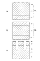
図1は、第1実施形態に係る半導体装置の模式図であり、(a)は、平面模式図、(b)は、(a)のX−Y位置における断面模式図と、不純物濃度プロファイルである。
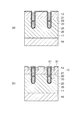
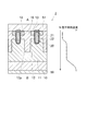
図2〜図4は、半導体装置の製造方法を説明するための断面模式図である。
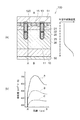
図8は、第2実施形態に係る半導体装置の断面模式図と、不純物濃度プロファイルである。
10 ドレイン層
11、11a ドリフト層
12、120 ベース層
12p 半導体層
13 ソース層
15 コンタクト層
19A、19B 半導体積層体
20 トレンチ
21 ゲート絶縁膜
22 ゲート電極
25 フィールドプレート絶縁膜
26 フィールドプレート電極
50 ドレイン電極
51 ソース電極
80、81 マスク部材
Claims (5)
- 第1導電型のドリフト層と、
前記ドリフト層の上に設けられた第2導電型のベース層と、
前記ベース層の表面に選択的に設けられた第1導電型のソース層と、
前記ソース層および前記ベース層を貫通し、前記ドリフト層に到達するトレンチ内に、ゲート絶縁膜を介して設けられたゲート電極と、
前記トレンチ内において、前記ゲート電極の下側に、フィールドプレート絶縁膜を介して設けられたフィールドプレート電極と、
前記ソース層に隣接するように前記ベース層の表面に選択的に設けられた第2導電型のコンタクト層と、
前記ドリフト層に電気的に接続されたドレイン電極と、
前記ソース層に電気的に接続されたソース電極と、
を備え、
前記フィールドプレート電極は、前記ソース電極に電気的に接続され、
前記コンタクト層に含まれる第2導電型の不純物濃度は、前記ベース層に含まれる前記第2導電型の不純物濃度から前記ベース層に含まれる前記第1導電型の不純物濃度を差し引いた値よりも高く、
前記コンタクト層は、前記ソース電極に接続され、
前記ベース層に含まれる前記第1導電型の不純物濃度は、前記ドリフト層に含まれる前記第1導電型の不純物濃度よりも低く、
前記ドリフト層に含まれる前記第1導電型の不純物濃度は、1×10¹⁶(atoms/cm3)以上であることを特徴とする半導体装置。 - 第1導電型のドリフト層と、
前記ドリフト層の上に設けられた第2導電型のベース層と、
前記ベース層の表面に選択的に設けられた第1導電型のソース層と、
前記ソース層および前記ベース層を貫通し、前記ドリフト層に到達するトレンチ内に、ゲート絶縁膜を介して設けられたゲート電極と、
前記トレンチ内において、前記ゲート電極の下側に、フィールドプレート絶縁膜を介して設けられたフィールドプレート電極と、
前記ドリフト層に電気的に接続されたドレイン電極と、
前記ソース層に電気的に接続されたソース電極と、
を備え、
前記フィールドプレート電極は、前記ソース電極に電気的に接続され、
前記ベース層に含まれる前記第1導電型の不純物濃度は、前記ドリフト層に含まれる前記第1導電型の不純物濃度よりも低く、
前記ドリフト層に含まれる前記第1導電型の不純物濃度は、1×10¹⁶(atoms/cm3)以上であることを特徴とする半導体装置。 - 第1導電型のドリフト層と、
前記ドリフト層の上に設けられた第2導電型のベース層と、
前記ベース層の表面に選択的に設けられた第1導電型のソース層と、
前記ソース層および前記ベース層を貫通し、前記ドリフト層に到達するトレンチ内にゲート絶縁膜を介して設けられたゲート電極と、
前記ベース層に接続され、前記ドリフト層の表面から内部にかけて設けられたピラー状の第2導電型の半導体層と、
前記ドリフト層に電気的に接続されたドレイン電極と、
前記ソース層に電気的に接続されたソース電極と、
を備え、
前記ベース層に含まれる前記第1導電型の不純物濃度は、前記ドリフト層に含まれる前記第1導電型の不純物濃度よりも低く、
前記ドリフト層に含まれる前記第1導電型の不純物濃度は、1×10¹⁶(atoms/cm3)以上であることを特徴とする半導体装置。 - 前記ソース層に隣接するように、前記ベース層の表面に第2導電型のコンタクト層がさらに選択的に設けられ、
前記コンタクト層に含まれる第2導電型の不純物濃度は、前記ベース層に含まれる前記第2導電型の不純物濃度から前記ベース層に含まれる前記第1導電型の不純物濃度を差し引いた値よりも高く、
前記コンタクト層は、前記ソース電極に接続されていることを特徴とする請求項2または3に記載の半導体装置。 - 第1導電型のドリフト層と、前記ドリフト層の上に設けられた第2導電型のベース層と、を有する半導体積層体を準備する工程と、
前記ベース層を貫通し、前記ドリフト層に到達するトレンチを形成する工程と、
前記トレンチ内において、フィールドプレート絶縁膜を介して設けられたフィールドプレート電極を形成する工程と、
前記トレンチ内において、前記フィールドプレート電極の上に、ゲート絶縁膜を介してゲート電極を形成する工程と、
前記ベース層の表面に、前記ゲート絶縁膜に接するように、第1導電型のソース層を選択的に型成する工程と、
前記ソース層および前記フィールドプレート電極に電気的に接続されるソース電極と、前記ドリフト層に電気的に接続されるドレイン電極と、を形成する工程と、
を備え、
前記ベース層に含まれる前記第1導電型の不純物濃度は、前記ドリフト層に含まれる前記第1導電型の不純物濃度よりも低く、
前記ドリフト層に含まれる前記第1導電型の不純物濃度は、1×10¹⁶(atoms/cm3)以上であることを特徴とする半導体装置の製造方法。
Priority Applications (4)
| Application Number | Priority Date | Filing Date | Title |
|---|---|---|---|
| JP2011068275A JP2012204636A (ja) | 2011-03-25 | 2011-03-25 | 半導体装置およびその製造方法 |
| CN2011102515121A CN102694022A (zh) | 2011-03-25 | 2011-08-29 | 半导体装置及其制造方法 |
| US13/239,248 US8643095B2 (en) | 2011-03-25 | 2011-09-21 | Semiconductor transistor device and method for manufacturing same |
| US14/141,279 US9236468B2 (en) | 2011-03-25 | 2013-12-26 | Semiconductor transistor device and method for manufacturing same |
Applications Claiming Priority (1)
| Application Number | Priority Date | Filing Date | Title |
|---|---|---|---|
| JP2011068275A JP2012204636A (ja) | 2011-03-25 | 2011-03-25 | 半導体装置およびその製造方法 |
Related Child Applications (1)
| Application Number | Title | Priority Date | Filing Date |
|---|---|---|---|
| JP2015256263A Division JP6317727B2 (ja) | 2015-12-28 | 2015-12-28 | 半導体装置 |
Publications (1)
| Publication Number | Publication Date |
|---|---|
| JP2012204636A true JP2012204636A (ja) | 2012-10-22 |
Family
ID=46859374
Family Applications (1)
| Application Number | Title | Priority Date | Filing Date |
|---|---|---|---|
| JP2011068275A Pending JP2012204636A (ja) | 2011-03-25 | 2011-03-25 | 半導体装置およびその製造方法 |
Country Status (3)
| Country | Link |
|---|---|
| US (2) | US8643095B2 (ja) |
| JP (1) | JP2012204636A (ja) |
| CN (1) | CN102694022A (ja) |
Cited By (3)
| Publication number | Priority date | Publication date | Assignee | Title |
|---|---|---|---|---|
| WO2016132552A1 (ja) * | 2015-02-20 | 2016-08-25 | 新電元工業株式会社 | 半導体装置 |
| US9831335B2 (en) | 2015-02-20 | 2017-11-28 | Shindengen Electric Manufacturing Co., Ltd. | Semiconductor device |
| WO2022004807A1 (ja) * | 2020-07-03 | 2022-01-06 | 株式会社デンソー | 半導体装置 |
Families Citing this family (7)
| Publication number | Priority date | Publication date | Assignee | Title |
|---|---|---|---|---|
| US8748976B1 (en) * | 2013-03-06 | 2014-06-10 | Texas Instruments Incorporated | Dual RESURF trench field plate in vertical MOSFET |
| US20140273374A1 (en) * | 2013-03-15 | 2014-09-18 | Joseph Yedinak | Vertical Doping and Capacitive Balancing for Power Semiconductor Devices |
| US9960269B2 (en) * | 2016-02-02 | 2018-05-01 | Renesas Electronics Corporation | Semiconductor device and method of manufacturing the same |
| JP7010184B2 (ja) * | 2018-09-13 | 2022-01-26 | 株式会社デンソー | 半導体装置 |
| JP7193371B2 (ja) * | 2019-02-19 | 2022-12-20 | 株式会社東芝 | 半導体装置 |
| JP7224979B2 (ja) | 2019-03-15 | 2023-02-20 | 株式会社東芝 | 半導体装置 |
| CN112447822A (zh) * | 2019-09-03 | 2021-03-05 | 苏州东微半导体股份有限公司 | 一种半导体功率器件 |
Citations (5)
| Publication number | Priority date | Publication date | Assignee | Title |
|---|---|---|---|---|
| JPH08250731A (ja) * | 1994-12-30 | 1996-09-27 | Siliconix Inc | 高いブレークダウン電圧と低いオン抵抗を兼ね備えたトレンチ型mosfet |
| JP2002083963A (ja) * | 2000-06-30 | 2002-03-22 | Toshiba Corp | 半導体素子 |
| JP2002528916A (ja) * | 1998-10-26 | 2002-09-03 | ノース・キャロライナ・ステイト・ユニヴァーシティ | 改良された高周波スイッチング特性と降伏特性を備えたパワー半導体デバイス |
| JP2004502306A (ja) * | 2000-06-23 | 2004-01-22 | シリコン・ワイヤレス・コーポレイション | 速度飽和モードでの動作時に線形伝達特性を持つmosfetデバイスとその製造方法及び動作方法 |
| JP2007103902A (ja) * | 2005-09-07 | 2007-04-19 | Nec Electronics Corp | 半導体装置 |
Family Cites Families (9)
| Publication number | Priority date | Publication date | Assignee | Title |
|---|---|---|---|---|
| US6316806B1 (en) * | 1999-03-31 | 2001-11-13 | Fairfield Semiconductor Corporation | Trench transistor with a self-aligned source |
| US6285060B1 (en) * | 1999-12-30 | 2001-09-04 | Siliconix Incorporated | Barrier accumulation-mode MOSFET |
| US6569738B2 (en) * | 2001-07-03 | 2003-05-27 | Siliconix, Inc. | Process for manufacturing trench gated MOSFET having drain/drift region |
| US7122860B2 (en) * | 2002-05-31 | 2006-10-17 | Koninklijke Philips Electronics N.V. | Trench-gate semiconductor devices |
| US7638841B2 (en) * | 2003-05-20 | 2009-12-29 | Fairchild Semiconductor Corporation | Power semiconductor devices and methods of manufacture |
| JP4903055B2 (ja) * | 2003-12-30 | 2012-03-21 | フェアチャイルド・セミコンダクター・コーポレーション | パワー半導体デバイスおよびその製造方法 |
| JP2006080177A (ja) * | 2004-09-08 | 2006-03-23 | Sanyo Electric Co Ltd | 半導体装置およびその製造方法 |
| JP5530602B2 (ja) | 2008-04-09 | 2014-06-25 | ルネサスエレクトロニクス株式会社 | 半導体装置およびその製造方法 |
| US8247296B2 (en) * | 2009-12-09 | 2012-08-21 | Semiconductor Components Industries, Llc | Method of forming an insulated gate field effect transistor device having a shield electrode structure |
-
2011
- 2011-03-25 JP JP2011068275A patent/JP2012204636A/ja active Pending
- 2011-08-29 CN CN2011102515121A patent/CN102694022A/zh active Pending
- 2011-09-21 US US13/239,248 patent/US8643095B2/en active Active
-
2013
- 2013-12-26 US US14/141,279 patent/US9236468B2/en not_active Expired - Fee Related
Patent Citations (5)
| Publication number | Priority date | Publication date | Assignee | Title |
|---|---|---|---|---|
| JPH08250731A (ja) * | 1994-12-30 | 1996-09-27 | Siliconix Inc | 高いブレークダウン電圧と低いオン抵抗を兼ね備えたトレンチ型mosfet |
| JP2002528916A (ja) * | 1998-10-26 | 2002-09-03 | ノース・キャロライナ・ステイト・ユニヴァーシティ | 改良された高周波スイッチング特性と降伏特性を備えたパワー半導体デバイス |
| JP2004502306A (ja) * | 2000-06-23 | 2004-01-22 | シリコン・ワイヤレス・コーポレイション | 速度飽和モードでの動作時に線形伝達特性を持つmosfetデバイスとその製造方法及び動作方法 |
| JP2002083963A (ja) * | 2000-06-30 | 2002-03-22 | Toshiba Corp | 半導体素子 |
| JP2007103902A (ja) * | 2005-09-07 | 2007-04-19 | Nec Electronics Corp | 半導体装置 |
Cited By (6)
| Publication number | Priority date | Publication date | Assignee | Title |
|---|---|---|---|---|
| WO2016132552A1 (ja) * | 2015-02-20 | 2016-08-25 | 新電元工業株式会社 | 半導体装置 |
| JPWO2016132552A1 (ja) * | 2015-02-20 | 2017-04-27 | 新電元工業株式会社 | 半導体装置 |
| US9831335B2 (en) | 2015-02-20 | 2017-11-28 | Shindengen Electric Manufacturing Co., Ltd. | Semiconductor device |
| US9831337B2 (en) | 2015-02-20 | 2017-11-28 | Shindengen Electric Manufacturing Co., Ltd. | Semiconductor device |
| WO2022004807A1 (ja) * | 2020-07-03 | 2022-01-06 | 株式会社デンソー | 半導体装置 |
| JP7364081B2 (ja) | 2020-07-03 | 2023-10-18 | 株式会社デンソー | 半導体装置 |
Also Published As
| Publication number | Publication date |
|---|---|
| US9236468B2 (en) | 2016-01-12 |
| US8643095B2 (en) | 2014-02-04 |
| CN102694022A (zh) | 2012-09-26 |
| US20120241851A1 (en) | 2012-09-27 |
| US20140103427A1 (en) | 2014-04-17 |
Similar Documents
| Publication | Publication Date | Title |
|---|---|---|
| US8643095B2 (en) | Semiconductor transistor device and method for manufacturing same | |
| US7928505B2 (en) | Semiconductor device with vertical trench and lightly doped region | |
| JP6048317B2 (ja) | 炭化珪素半導体装置 | |
| JP5586887B2 (ja) | 半導体装置及びその製造方法 | |
| US20150179764A1 (en) | Semiconductor device and method for manufacturing same | |
| US8174066B2 (en) | Semiconductor device and method of manufacturing semiconductor device | |
| JP5717661B2 (ja) | 半導体装置とその製造方法 | |
| US8373247B2 (en) | Semiconductor device | |
| US9312337B2 (en) | Semiconductor device | |
| JP2016167519A (ja) | 半導体装置 | |
| US20130056790A1 (en) | Semiconductor device and method for manufacturing same | |
| KR20080044127A (ko) | 고전압 반도체 소자 및 그 제조 방법 | |
| WO2015141212A1 (ja) | 半導体装置 | |
| US10381436B2 (en) | Semiconductor device and method of manufacturing semiconductor device | |
| JP2015133380A (ja) | 半導体装置 | |
| JP2015138958A (ja) | 炭化珪素半導体装置の製造方法 | |
| JP2016039263A (ja) | 半導体装置の製造方法 | |
| KR20100027056A (ko) | 반도체 장치 및 그의 제조 방법 | |
| JP2018046161A (ja) | 半導体装置および半導体装置の製造方法 | |
| WO2018147466A1 (ja) | 半導体装置 | |
| JP6317727B2 (ja) | 半導体装置 | |
| CN102694010A (zh) | 半导体元件 | |
| JP2014187200A (ja) | 半導体装置の製造方法 | |
| KR20120074492A (ko) | 반도체 소자 및 그 수퍼정션 구조 형성 방법 | |
| CN116799060A (zh) | 半导体装置及其制造方法 |
Legal Events
| Date | Code | Title | Description |
|---|---|---|---|
| A621 | Written request for application examination |
Free format text: JAPANESE INTERMEDIATE CODE: A621 Effective date: 20130225 |
|
| A977 | Report on retrieval |
Free format text: JAPANESE INTERMEDIATE CODE: A971007 Effective date: 20130708 |
|
| A131 | Notification of reasons for refusal |
Free format text: JAPANESE INTERMEDIATE CODE: A131 Effective date: 20130814 |
|
| A521 | Written amendment |
Free format text: JAPANESE INTERMEDIATE CODE: A523 Effective date: 20131011 |
|
| A131 | Notification of reasons for refusal |
Free format text: JAPANESE INTERMEDIATE CODE: A131 Effective date: 20140502 |
|
| A521 | Written amendment |
Free format text: JAPANESE INTERMEDIATE CODE: A523 Effective date: 20140625 |
|
| A131 | Notification of reasons for refusal |
Free format text: JAPANESE INTERMEDIATE CODE: A131 Effective date: 20150129 |
|
| A521 | Written amendment |
Free format text: JAPANESE INTERMEDIATE CODE: A523 Effective date: 20150330 |
|
| A02 | Decision of refusal |
Free format text: JAPANESE INTERMEDIATE CODE: A02 Effective date: 20151002 |