WO2022004807A1 - 半導体装置 - Google Patents
半導体装置 Download PDFInfo
- Publication number
- WO2022004807A1 WO2022004807A1 PCT/JP2021/024812 JP2021024812W WO2022004807A1 WO 2022004807 A1 WO2022004807 A1 WO 2022004807A1 JP 2021024812 W JP2021024812 W JP 2021024812W WO 2022004807 A1 WO2022004807 A1 WO 2022004807A1
- Authority
- WO
- WIPO (PCT)
- Prior art keywords
- layer
- cell region
- region
- sense
- channel
- Prior art date
Links
- 239000004065 semiconductor Substances 0.000 title claims abstract description 58
- 239000010410 layer Substances 0.000 claims description 127
- 239000012535 impurity Substances 0.000 claims description 55
- 239000002344 surface layer Substances 0.000 claims description 5
- 239000000758 substrate Substances 0.000 description 10
- 238000001514 detection method Methods 0.000 description 5
- 238000012986 modification Methods 0.000 description 5
- 230000004048 modification Effects 0.000 description 5
- 230000015572 biosynthetic process Effects 0.000 description 4
- 239000011229 interlayer Substances 0.000 description 4
- 230000035945 sensitivity Effects 0.000 description 3
- 239000004020 conductor Substances 0.000 description 1
- 230000001419 dependent effect Effects 0.000 description 1
- 238000010586 diagram Methods 0.000 description 1
- 230000000694 effects Effects 0.000 description 1
- 239000000463 material Substances 0.000 description 1
- 230000000149 penetrating effect Effects 0.000 description 1
- 229910021420 polycrystalline silicon Inorganic materials 0.000 description 1
- 229910052710 silicon Inorganic materials 0.000 description 1
- 239000010703 silicon Substances 0.000 description 1
Images


Classifications
-
- H—ELECTRICITY
- H01—ELECTRIC ELEMENTS
- H01L—SEMICONDUCTOR DEVICES NOT COVERED BY CLASS H10
- H01L29/00—Semiconductor devices adapted for rectifying, amplifying, oscillating or switching, or capacitors or resistors with at least one potential-jump barrier or surface barrier, e.g. PN junction depletion layer or carrier concentration layer; Details of semiconductor bodies or of electrodes thereof ; Multistep manufacturing processes therefor
- H01L29/66—Types of semiconductor device ; Multistep manufacturing processes therefor
- H01L29/68—Types of semiconductor device ; Multistep manufacturing processes therefor controllable by only the electric current supplied, or only the electric potential applied, to an electrode which does not carry the current to be rectified, amplified or switched
- H01L29/76—Unipolar devices, e.g. field effect transistors
- H01L29/772—Field effect transistors
- H01L29/78—Field effect transistors with field effect produced by an insulated gate
- H01L29/7801—DMOS transistors, i.e. MISFETs with a channel accommodating body or base region adjoining a drain drift region
- H01L29/7802—Vertical DMOS transistors, i.e. VDMOS transistors
- H01L29/7815—Vertical DMOS transistors, i.e. VDMOS transistors with voltage or current sensing structure, e.g. emulator section, overcurrent sensing cell
-
- H—ELECTRICITY
- H01—ELECTRIC ELEMENTS
- H01L—SEMICONDUCTOR DEVICES NOT COVERED BY CLASS H10
- H01L29/00—Semiconductor devices adapted for rectifying, amplifying, oscillating or switching, or capacitors or resistors with at least one potential-jump barrier or surface barrier, e.g. PN junction depletion layer or carrier concentration layer; Details of semiconductor bodies or of electrodes thereof ; Multistep manufacturing processes therefor
- H01L29/02—Semiconductor bodies ; Multistep manufacturing processes therefor
- H01L29/06—Semiconductor bodies ; Multistep manufacturing processes therefor characterised by their shape; characterised by the shapes, relative sizes, or dispositions of the semiconductor regions ; characterised by the concentration or distribution of impurities within semiconductor regions
- H01L29/0603—Semiconductor bodies ; Multistep manufacturing processes therefor characterised by their shape; characterised by the shapes, relative sizes, or dispositions of the semiconductor regions ; characterised by the concentration or distribution of impurities within semiconductor regions characterised by particular constructional design considerations, e.g. for preventing surface leakage, for controlling electric field concentration or for internal isolations regions
- H01L29/0607—Semiconductor bodies ; Multistep manufacturing processes therefor characterised by their shape; characterised by the shapes, relative sizes, or dispositions of the semiconductor regions ; characterised by the concentration or distribution of impurities within semiconductor regions characterised by particular constructional design considerations, e.g. for preventing surface leakage, for controlling electric field concentration or for internal isolations regions for preventing surface leakage or controlling electric field concentration
- H01L29/0611—Semiconductor bodies ; Multistep manufacturing processes therefor characterised by their shape; characterised by the shapes, relative sizes, or dispositions of the semiconductor regions ; characterised by the concentration or distribution of impurities within semiconductor regions characterised by particular constructional design considerations, e.g. for preventing surface leakage, for controlling electric field concentration or for internal isolations regions for preventing surface leakage or controlling electric field concentration for increasing or controlling the breakdown voltage of reverse biased devices
- H01L29/0615—Semiconductor bodies ; Multistep manufacturing processes therefor characterised by their shape; characterised by the shapes, relative sizes, or dispositions of the semiconductor regions ; characterised by the concentration or distribution of impurities within semiconductor regions characterised by particular constructional design considerations, e.g. for preventing surface leakage, for controlling electric field concentration or for internal isolations regions for preventing surface leakage or controlling electric field concentration for increasing or controlling the breakdown voltage of reverse biased devices by the doping profile or the shape or the arrangement of the PN junction, or with supplementary regions, e.g. junction termination extension [JTE]
- H01L29/0619—Semiconductor bodies ; Multistep manufacturing processes therefor characterised by their shape; characterised by the shapes, relative sizes, or dispositions of the semiconductor regions ; characterised by the concentration or distribution of impurities within semiconductor regions characterised by particular constructional design considerations, e.g. for preventing surface leakage, for controlling electric field concentration or for internal isolations regions for preventing surface leakage or controlling electric field concentration for increasing or controlling the breakdown voltage of reverse biased devices by the doping profile or the shape or the arrangement of the PN junction, or with supplementary regions, e.g. junction termination extension [JTE] with a supplementary region doped oppositely to or in rectifying contact with the semiconductor containing or contacting region, e.g. guard rings with PN or Schottky junction
- H01L29/0623—Buried supplementary region, e.g. buried guard ring
-
- H—ELECTRICITY
- H01—ELECTRIC ELEMENTS
- H01L—SEMICONDUCTOR DEVICES NOT COVERED BY CLASS H10
- H01L29/00—Semiconductor devices adapted for rectifying, amplifying, oscillating or switching, or capacitors or resistors with at least one potential-jump barrier or surface barrier, e.g. PN junction depletion layer or carrier concentration layer; Details of semiconductor bodies or of electrodes thereof ; Multistep manufacturing processes therefor
- H01L29/02—Semiconductor bodies ; Multistep manufacturing processes therefor
- H01L29/06—Semiconductor bodies ; Multistep manufacturing processes therefor characterised by their shape; characterised by the shapes, relative sizes, or dispositions of the semiconductor regions ; characterised by the concentration or distribution of impurities within semiconductor regions
- H01L29/0684—Semiconductor bodies ; Multistep manufacturing processes therefor characterised by their shape; characterised by the shapes, relative sizes, or dispositions of the semiconductor regions ; characterised by the concentration or distribution of impurities within semiconductor regions characterised by the shape, relative sizes or dispositions of the semiconductor regions or junctions between the regions
- H01L29/0692—Surface layout
- H01L29/0696—Surface layout of cellular field-effect devices, e.g. multicellular DMOS transistors or IGBTs
-
- H—ELECTRICITY
- H01—ELECTRIC ELEMENTS
- H01L—SEMICONDUCTOR DEVICES NOT COVERED BY CLASS H10
- H01L29/00—Semiconductor devices adapted for rectifying, amplifying, oscillating or switching, or capacitors or resistors with at least one potential-jump barrier or surface barrier, e.g. PN junction depletion layer or carrier concentration layer; Details of semiconductor bodies or of electrodes thereof ; Multistep manufacturing processes therefor
- H01L29/02—Semiconductor bodies ; Multistep manufacturing processes therefor
- H01L29/06—Semiconductor bodies ; Multistep manufacturing processes therefor characterised by their shape; characterised by the shapes, relative sizes, or dispositions of the semiconductor regions ; characterised by the concentration or distribution of impurities within semiconductor regions
- H01L29/08—Semiconductor bodies ; Multistep manufacturing processes therefor characterised by their shape; characterised by the shapes, relative sizes, or dispositions of the semiconductor regions ; characterised by the concentration or distribution of impurities within semiconductor regions with semiconductor regions connected to an electrode carrying current to be rectified, amplified or switched and such electrode being part of a semiconductor device which comprises three or more electrodes
- H01L29/0843—Source or drain regions of field-effect devices
- H01L29/0847—Source or drain regions of field-effect devices of field-effect transistors with insulated gate
- H01L29/0852—Source or drain regions of field-effect devices of field-effect transistors with insulated gate of DMOS transistors
- H01L29/0873—Drain regions
- H01L29/0878—Impurity concentration or distribution
-
- H—ELECTRICITY
- H01—ELECTRIC ELEMENTS
- H01L—SEMICONDUCTOR DEVICES NOT COVERED BY CLASS H10
- H01L29/00—Semiconductor devices adapted for rectifying, amplifying, oscillating or switching, or capacitors or resistors with at least one potential-jump barrier or surface barrier, e.g. PN junction depletion layer or carrier concentration layer; Details of semiconductor bodies or of electrodes thereof ; Multistep manufacturing processes therefor
- H01L29/02—Semiconductor bodies ; Multistep manufacturing processes therefor
- H01L29/06—Semiconductor bodies ; Multistep manufacturing processes therefor characterised by their shape; characterised by the shapes, relative sizes, or dispositions of the semiconductor regions ; characterised by the concentration or distribution of impurities within semiconductor regions
- H01L29/10—Semiconductor bodies ; Multistep manufacturing processes therefor characterised by their shape; characterised by the shapes, relative sizes, or dispositions of the semiconductor regions ; characterised by the concentration or distribution of impurities within semiconductor regions with semiconductor regions connected to an electrode not carrying current to be rectified, amplified or switched and such electrode being part of a semiconductor device which comprises three or more electrodes
- H01L29/1025—Channel region of field-effect devices
-
- H—ELECTRICITY
- H01—ELECTRIC ELEMENTS
- H01L—SEMICONDUCTOR DEVICES NOT COVERED BY CLASS H10
- H01L29/00—Semiconductor devices adapted for rectifying, amplifying, oscillating or switching, or capacitors or resistors with at least one potential-jump barrier or surface barrier, e.g. PN junction depletion layer or carrier concentration layer; Details of semiconductor bodies or of electrodes thereof ; Multistep manufacturing processes therefor
- H01L29/02—Semiconductor bodies ; Multistep manufacturing processes therefor
- H01L29/36—Semiconductor bodies ; Multistep manufacturing processes therefor characterised by the concentration or distribution of impurities in the bulk material
-
- H—ELECTRICITY
- H01—ELECTRIC ELEMENTS
- H01L—SEMICONDUCTOR DEVICES NOT COVERED BY CLASS H10
- H01L29/00—Semiconductor devices adapted for rectifying, amplifying, oscillating or switching, or capacitors or resistors with at least one potential-jump barrier or surface barrier, e.g. PN junction depletion layer or carrier concentration layer; Details of semiconductor bodies or of electrodes thereof ; Multistep manufacturing processes therefor
- H01L29/40—Electrodes ; Multistep manufacturing processes therefor
- H01L29/41—Electrodes ; Multistep manufacturing processes therefor characterised by their shape, relative sizes or dispositions
- H01L29/423—Electrodes ; Multistep manufacturing processes therefor characterised by their shape, relative sizes or dispositions not carrying the current to be rectified, amplified or switched
- H01L29/42312—Gate electrodes for field effect devices
- H01L29/42316—Gate electrodes for field effect devices for field-effect transistors
- H01L29/4232—Gate electrodes for field effect devices for field-effect transistors with insulated gate
- H01L29/42356—Disposition, e.g. buried gate electrode
- H01L29/4236—Disposition, e.g. buried gate electrode within a trench, e.g. trench gate electrode, groove gate electrode
-
- H—ELECTRICITY
- H01—ELECTRIC ELEMENTS
- H01L—SEMICONDUCTOR DEVICES NOT COVERED BY CLASS H10
- H01L29/00—Semiconductor devices adapted for rectifying, amplifying, oscillating or switching, or capacitors or resistors with at least one potential-jump barrier or surface barrier, e.g. PN junction depletion layer or carrier concentration layer; Details of semiconductor bodies or of electrodes thereof ; Multistep manufacturing processes therefor
- H01L29/66—Types of semiconductor device ; Multistep manufacturing processes therefor
- H01L29/66007—Multistep manufacturing processes
- H01L29/66075—Multistep manufacturing processes of devices having semiconductor bodies comprising group 14 or group 13/15 materials
- H01L29/66227—Multistep manufacturing processes of devices having semiconductor bodies comprising group 14 or group 13/15 materials the devices being controllable only by the electric current supplied or the electric potential applied, to an electrode which does not carry the current to be rectified, amplified or switched, e.g. three-terminal devices
- H01L29/66234—Bipolar junction transistors [BJT]
- H01L29/66325—Bipolar junction transistors [BJT] controlled by field-effect, e.g. insulated gate bipolar transistors [IGBT]
- H01L29/66333—Vertical insulated gate bipolar transistors
- H01L29/66348—Vertical insulated gate bipolar transistors with a recessed gate
-
- H—ELECTRICITY
- H01—ELECTRIC ELEMENTS
- H01L—SEMICONDUCTOR DEVICES NOT COVERED BY CLASS H10
- H01L29/00—Semiconductor devices adapted for rectifying, amplifying, oscillating or switching, or capacitors or resistors with at least one potential-jump barrier or surface barrier, e.g. PN junction depletion layer or carrier concentration layer; Details of semiconductor bodies or of electrodes thereof ; Multistep manufacturing processes therefor
- H01L29/66—Types of semiconductor device ; Multistep manufacturing processes therefor
- H01L29/66007—Multistep manufacturing processes
- H01L29/66075—Multistep manufacturing processes of devices having semiconductor bodies comprising group 14 or group 13/15 materials
- H01L29/66227—Multistep manufacturing processes of devices having semiconductor bodies comprising group 14 or group 13/15 materials the devices being controllable only by the electric current supplied or the electric potential applied, to an electrode which does not carry the current to be rectified, amplified or switched, e.g. three-terminal devices
- H01L29/66409—Unipolar field-effect transistors
- H01L29/66477—Unipolar field-effect transistors with an insulated gate, i.e. MISFET
- H01L29/66674—DMOS transistors, i.e. MISFETs with a channel accommodating body or base region adjoining a drain drift region
- H01L29/66712—Vertical DMOS transistors, i.e. VDMOS transistors
- H01L29/66734—Vertical DMOS transistors, i.e. VDMOS transistors with a step of recessing the gate electrode, e.g. to form a trench gate electrode
-
- H—ELECTRICITY
- H01—ELECTRIC ELEMENTS
- H01L—SEMICONDUCTOR DEVICES NOT COVERED BY CLASS H10
- H01L29/00—Semiconductor devices adapted for rectifying, amplifying, oscillating or switching, or capacitors or resistors with at least one potential-jump barrier or surface barrier, e.g. PN junction depletion layer or carrier concentration layer; Details of semiconductor bodies or of electrodes thereof ; Multistep manufacturing processes therefor
- H01L29/66—Types of semiconductor device ; Multistep manufacturing processes therefor
- H01L29/68—Types of semiconductor device ; Multistep manufacturing processes therefor controllable by only the electric current supplied, or only the electric potential applied, to an electrode which does not carry the current to be rectified, amplified or switched
- H01L29/70—Bipolar devices
- H01L29/72—Transistor-type devices, i.e. able to continuously respond to applied control signals
- H01L29/739—Transistor-type devices, i.e. able to continuously respond to applied control signals controlled by field-effect, e.g. bipolar static induction transistors [BSIT]
- H01L29/7393—Insulated gate bipolar mode transistors, i.e. IGBT; IGT; COMFET
- H01L29/7395—Vertical transistors, e.g. vertical IGBT
- H01L29/7396—Vertical transistors, e.g. vertical IGBT with a non planar surface, e.g. with a non planar gate or with a trench or recess or pillar in the surface of the emitter, base or collector region for improving current density or short circuiting the emitter and base regions
- H01L29/7397—Vertical transistors, e.g. vertical IGBT with a non planar surface, e.g. with a non planar gate or with a trench or recess or pillar in the surface of the emitter, base or collector region for improving current density or short circuiting the emitter and base regions and a gate structure lying on a slanted or vertical surface or formed in a groove, e.g. trench gate IGBT
-
- H—ELECTRICITY
- H01—ELECTRIC ELEMENTS
- H01L—SEMICONDUCTOR DEVICES NOT COVERED BY CLASS H10
- H01L29/00—Semiconductor devices adapted for rectifying, amplifying, oscillating or switching, or capacitors or resistors with at least one potential-jump barrier or surface barrier, e.g. PN junction depletion layer or carrier concentration layer; Details of semiconductor bodies or of electrodes thereof ; Multistep manufacturing processes therefor
- H01L29/66—Types of semiconductor device ; Multistep manufacturing processes therefor
- H01L29/68—Types of semiconductor device ; Multistep manufacturing processes therefor controllable by only the electric current supplied, or only the electric potential applied, to an electrode which does not carry the current to be rectified, amplified or switched
- H01L29/76—Unipolar devices, e.g. field effect transistors
- H01L29/772—Field effect transistors
- H01L29/78—Field effect transistors with field effect produced by an insulated gate
- H01L29/7801—DMOS transistors, i.e. MISFETs with a channel accommodating body or base region adjoining a drain drift region
- H01L29/7802—Vertical DMOS transistors, i.e. VDMOS transistors
- H01L29/7813—Vertical DMOS transistors, i.e. VDMOS transistors with trench gate electrode, e.g. UMOS transistors
-
- H—ELECTRICITY
- H01—ELECTRIC ELEMENTS
- H01L—SEMICONDUCTOR DEVICES NOT COVERED BY CLASS H10
- H01L29/00—Semiconductor devices adapted for rectifying, amplifying, oscillating or switching, or capacitors or resistors with at least one potential-jump barrier or surface barrier, e.g. PN junction depletion layer or carrier concentration layer; Details of semiconductor bodies or of electrodes thereof ; Multistep manufacturing processes therefor
- H01L29/40—Electrodes ; Multistep manufacturing processes therefor
- H01L29/402—Field plates
- H01L29/407—Recessed field plates, e.g. trench field plates, buried field plates
Definitions
- the present disclosure relates to a semiconductor device provided with a vertical semiconductor switching element having the same structure in a main cell region and a sense cell region, and detects a current flowing in the main cell region based on the current flowing in the sense cell region.
- Patent Document 1 discloses a semiconductor device in which a vertical semiconductor switching element having the same structure is provided in a main cell region and a sense cell region, and a current flowing in the main cell region is detected based on the current flowing in the sense cell region. ..
- This semiconductor device has a planar type gate electrode and has a structure in which a current detection element is arranged as a sense cell region between main elements formed in the main cell region, and has a high resistance between the main element and the sense element. By providing a region, they are electrically separated from each other. With such a structure, the passage of the carrier is matched, and the accuracy of the detection current flowing through the current detection element is improved.
- a vertical semiconductor switching element having the same structure is formed in a main cell region and a sense cell region, and the semiconductor switching element is a first conductive type drift layer and a drift.
- a second conductive type channel layer formed on the layer, a first conductive type first impurity region formed on the surface layer portion of the channel layer in the channel layer and having a higher impurity concentration than the drift layer, and a first.
- a gate insulating film that covers the channel layer between the impurity region and the drift layer, and a plurality of lines arranged in a striped manner with one direction as the longitudinal direction are arranged in a stripe shape and formed on the surface of the gate insulating film.
- a first or second conductive type second impurity formed on the side opposite to the channel layer with the drift layer sandwiched between the gate electrode layer forming the channel region with respect to the channel layer and having a higher impurity concentration than the drift layer. It is configured to have a region, an upper electrode electrically connected to the first impurity region and the channel layer, and a lower electrode electrically connected to the second impurity region.
- the sense cell region is defined as a rectangular region surrounding the operating region of the semiconductor switching element formed as a sense cell, and the dimension in the same direction as the one direction in the main cell region is defined as the lateral dimension and the lateral dimension.
- the dimension in the vertical direction is defined as the vertical dimension, and the vertical dimension is defined as greater than or equal to the horizontal dimension.
- the dimensions are designed so that the vertical dimension of the main cell area is equal to or greater than the horizontal dimension.
- the main current flowing in the main cell region is detected based on the ratio of the sense current flowing in the sense cell region (hereinafter referred to as the sense ratio) to the main current flowing in the main cell region. Therefore, if the amount of change in the sense ratio with respect to the change in the gate voltage is large, the sense ratio can be detected with high sensitivity and accuracy. Therefore, when considering a circuit that detects the sense ratio or sense current of a semiconductor device that drives a vertical semiconductor switching element in a feedback circuit, it is possible to improve the degree of freedom in circuit design in which the gate voltage is controlled by the gate driver circuit. Therefore, it is possible to design the gate voltage dependence.
- the semiconductor switching element includes a first conductive type drift layer, a second conductive type channel layer formed on the drift layer, and the channel layer in the channel layer.
- a first conductive type first impurity region formed on the surface layer and having a higher impurity concentration than the drift layer, and a gate insulating film covering the channel layer between the first impurity region and the drift layer, longitudinally oriented in one direction.
- a gate electrode layer that forms a channel region with respect to the channel layer by being arranged in a stripe shape by arranging a plurality of conductors in the direction and being formed on the surface of the gate insulating film, and a channel layer sandwiching a drift layer.
- a first or second conductive type second impurity region formed on the opposite side and having a higher impurity concentration than the drift layer, an upper electrode electrically connected to the first impurity region and the channel layer, and a second.
- a lower electrode electrically connected to an impurity region is provided, and a resistance component layer having a higher resistance than the drift layer in the main cell region is formed in the drift layer in the sense cell region.
- the drift layer in the sense cell region is provided with a resistance component layer. According to such a configuration, it is possible to reduce the sense current flowing in the sense cell region. Therefore, it is possible to make the gate voltage dependence of the sense cell region and the main cell region substantially the same. Therefore, it is possible to design the gate voltage dependence.
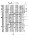
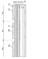
- FIG. 2 is a sectional view taken along line II-II of FIG.
- FIG. 3 is a sectional view taken along line III-III of FIG.
- FIG. 6 is a sectional view taken along line IV-IV of FIG.
- It is a top layout drawing explaining the sense cell area. It is a block diagram which showed the state of driving a semiconductor device by a gate driver circuit. It is a figure which showed the relationship of the sense ratio with respect to the gate voltage. It is a top layout drawing explaining the sense cell region in the semiconductor device which concerns on the modification of 1st Embodiment.
- the first embodiment will be described.
- a semiconductor device provided with an n-channel type vertical MOSFET as a vertical semiconductor switching element having the same structure in the main cell region and the sense cell region will be described.
- the structure of the semiconductor device according to the present embodiment will be described with reference to FIGS. 1 to 4.
- the semiconductor device is configured to have a main cell region Rm and a sense cell region Rs.
- the main cell region Rm is formed in a rectangular shape with a part cut off, and the sense cell region Rs is arranged in the main cell region Rm and is formed so as to be surrounded by the main cell region Rm.
- FIG. 1 shows only the vicinity of the sense cell region Rs in the main cell region Rm, the main cell region Rm actually has a sufficiently wider area than the sense cell region Rs, for example, an area of 100 million times. Has been done.
- An n-channel type vertical MOSFET having the same structure is formed in the main cell region Rm and the sense cell region Rs.
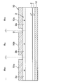
- the semiconductor device is formed by using an n + type semiconductor substrate 1 made of a semiconductor material such as silicon having a high impurity concentration.
- the semiconductor substrate 1 has a thickness of 10 to 300 ⁇ m and an n-type impurity concentration of about 1 ⁇ 10 12 to 1 ⁇ 10 18 cm -3 .
- n + -type impurity concentration than the semiconductor substrate 1 is a low density - type drift layer 2 is formed, n - the desired type drift layer 2
- a channel p-type layer 3 having a relatively low impurity concentration is formed at the position.
- the n - type drift layer 2 has, for example, a thickness of 1 to 10 ⁇ m and an n-type impurity concentration of about 1 ⁇ 10 12 to 1 ⁇ 10 18 cm -3 .
- the thickness of the channel p-type layer 3 is 0 to 2 ⁇ m, and the concentration of p-type impurities is about 1 ⁇ 10 12 to 1 ⁇ 10 18 cm -3 .
- the channel p-type layer 3 is formed by ion-implanting a p-type impurity into the n-type drift layer 2.
- the main channel layer 3a formed in the main cell region Rm and the sense channel layer 3b formed in the sense cell region Rs are continuously connected. It is said to be a structure.
- the surface layer portion of the channel p-type layer 3 is an n + -type impurity region 4 which is a region constituting the source region and corresponds to a first impurity region having a higher impurity concentration than the n-type drift layer 2. Is provided.
- the n + type impurity region 4 has, for example, a thickness of 0 to 2 ⁇ m and an n-type impurity concentration of about 1 ⁇ 10 12 to 1 ⁇ 10 18 cm -3 .
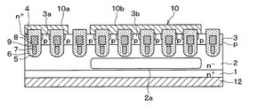
- a trench 5 is formed from the surface side of the substrate , penetrating the n + type impurity region 4 and the channel p type layer 3 and reaching the n ⁇ type drift layer 2.
- a gate insulating film 6 is formed so as to cover the inner wall surface of the trench 5, and a shield electrode 7 and a gate electrode layer 8 composed of doped Poly—Si are formed in the trench 5 via the gate insulating film 6. It is laminated to form a two-layer structure.
- the shield electrode 7 is formed to reduce the capacitance between the gate and the drain and improve the electrical characteristics of the MOSFET by being fixed to the source potential.
- the gate electrode layer 8 performs a MOSFET switching operation, and forms a channel in the channel p-type layer 3 on the side surface of the trench 5 when a gate voltage is applied.
- the trench gate structure is composed of the trench 5, the gate insulating film 6, the shield electrode 7, the gate electrode layer 8 and the insulating film 9.
- This trench gate structure has a striped layout in which, for example, a plurality of lines are arranged in the vertical direction of the paper surface in FIG. 2 as the longitudinal direction, or in the vertical direction of the paper surface in FIG. 2, or in the left-right direction of the paper surface in FIG.
- the formation pitch of the trench gate structure is arbitrary, but is set to, for example, 1 to 2 ⁇ m.
- n + type impurity region 4 is not formed, so that the vertical MOSFET is not formed. ..
- the trench 5 is in a state of being continuously connected by the main cell region Rm and the sense cell region Rs.
- the shield electrode 7 and the gate electrode layer 8 embedded in the trench 5 are also continuously connected to both the main cell region Rm and the sense cell region Rs.
- the shield electrode 7 is outside the main cell region Rm with respect to the gate electrode layer 8, that is, the sense cell region of the main cell region Rm. It extends to the side away from Rs. Then, the portion is exposed as a shield liner from the surface of the channel p-type layer 3, so that an electrical connection with the upper electrode 10 which is a source potential described later can be achieved.
- the gate electrode layer 8 extends beyond the shield electrode 7 to the outside of the main cell region Rm, that is, to the side of the main cell region Rm away from the sense region. There is. The portion is exposed from the surface of the channel p-type layer 3 as a gate liner, and is electrically connected to a gate electrode (not shown).
- an interlayer insulating film 13 composed of an oxide film or the like is formed so as to cover the gate electrode layer 8, and an upper electrode 10 corresponding to a source electrode and a gate electrode (not shown) are formed on the interlayer insulating film 13.
- the upper electrode 10 is electrically connected to the n + type impurity region 4 and the channel p-type layer 3 through a portion where the interlayer insulating film 13 is not formed, for example, a contact hole.
- the gate electrode is also electrically connected to the gate electrode layer 8 via a gate liner through a portion where the interlayer insulating film 13 is not formed, for example, a contact hole.
- the upper electrode 10 is divided into a main electrode 10a formed in the main cell region Rm and a sense electrode 10b formed in the sense cell region Rs, and these are separated by a predetermined distance.
- the main electrode 10a is formed over almost the entire area of the main cell region Rm, and is formed in a rectangular shape with a part cut out.
- the sense electrode 10b has a rectangular shape and is arranged so as to be surrounded by the main electrode 10a.
- the lead-out wiring 10c is drawn out from one side of the sense electrode 10b corresponding to the notched portion of the main cell region Rm to the outside of the main cell region Rm.
- a lower electrode 12 corresponding to a drain electrode is formed on the surface of the n + type semiconductor substrate 1 opposite to the n ⁇ type drift layer 2.
- the semiconductor device having the vertical MOSFET is configured.
- a gate voltage is applied to the gate electrode layer 8 of the vertical MOSFET provided in the main cell region Rm and the sense cell region Rs, a channel is generated on the surface of the channel p-type layer 3 in contact with the trench 5. It is formed.
- the electrons injected from the upper electrode 10 pass through the channel formed in the channel p-type layer 3 from the n + type impurity region 4 and then reach the n ⁇ type drift layer 2, and the upper electrode 10 and the lower electrode The operation of passing a current between the 12 and the 12 is performed.
- a vertical MOSFET having the same cell structure is formed in each of the main cell region Rm and the sense cell region Rs, and the cell area of the vertical MOSFET provided in the main cell region Rm and the sense cell region Rs, in other words, the number of cells is set to a predetermined ratio. It is set to. Therefore, the sense current obtained by reducing the main current flowing in the main cell region Rm by a predetermined ratio can be passed through the sense cell region Rs. Therefore, by outputting the sense current flowing in the sense cell region Rs to the outside, the sense current flowing in the main cell region Rm can be detected.
- the vertical direction is defined as the horizontal direction in the sense cell region Rs in the same direction as the longitudinal direction of the trench gate structure and the longitudinal direction in the direction perpendicular to the longitudinal direction. It defines the dimensional relationship between dimensions and lateral dimensions.
- the sense cell region Rs is a rectangular portion that is an operating region of the vertical MOSFET formed as a sense cell. That is, in the sense cell region Rs, the n + type impurity region 4 constituting the source region is formed along the trench gate structure, so that the MOS operation is performed when the gate voltage is applied to the gate electrode layer 8 and the current is generated. It is an area where the current flows.
- the sense cell region Rs is shown as a region that collectively surrounds a plurality of n + type impurity regions 4 that are brought into contact with the sense electrode 10b.
- the vertical dimension of the sense cell region Rs is set to be equal to or larger than the horizontal dimension, in other words, the ratio of the vertical dimension to the horizontal dimension of the sense cell region Rs is set to 1 or more. More preferably, the dimension of the portion serving as the current path (hereinafter referred to as the current path dimension) excluding the width of the trench gate structure from the vertical dimension of the sense cell region Rs is set to be equal to or larger than the horizontal dimension.
- the main current flowing in the main cell region Rm is detected based on the sense ratio. Specifically, as shown in FIG. 6, a gate voltage is applied from the gate driver circuit 100 to the semiconductor device 101 provided with the main cell region Rm and the sense cell region Rs, and the sense ratio or sense current at that time is gated. It feeds back to the driver circuit 100.
- the gate driver circuit 100 includes a feedback circuit, and the sense ratio or sense current is detected by the feedback circuit, and the gate voltage output by the gate driver circuit 100 is adjusted so that the desired main current is obtained. Control.
- FIG. 7 shows the dependence of the sense ratio on the gate voltage (Vgs) (hereinafter referred to as Vgs dependence).
- Vgs dependence the gate voltage
- the sense ratio has a Vgs dependence.
- the horizontal dimension is larger than the vertical dimension of the sense cell region Rs
- the change in the sense ratio with respect to the gate voltage of the element is small.
- the characteristic is that the sense ratio becomes smaller as the gate voltage becomes larger, the sense ratio becomes almost constant regardless of the magnitude of the gate voltage.
- the vertical dimension of the sense cell region Rs is larger than the horizontal dimension as in the present embodiment
- the change in the sense ratio with respect to the gate voltage of the element is large, and the larger the gate voltage is, the larger the sense ratio is. Becomes smaller.
- the larger the gate voltage the larger the rate of decrease in the sense ratio.
- the gate voltage dependence of the entire system including the resistance is suppressed by having the gate voltage dependence of the sense cell itself.
- the sense ratio can be detected with high sensitivity.
- the sense ratio or sense current is fed back to the gate driver circuit 100, but the sense ratio when the gate voltage is set to a predetermined value is fed back to adjust the gate voltage output by the gate driver circuit 100.
- the sense ratio can be detected with high sensitivity and accuracy. Therefore, when considering a circuit that detects the sense ratio or sense current of a semiconductor device that drives a vertical MOSFET in a feedback circuit, it is possible to improve the degree of freedom in circuit design in which the gate voltage is controlled by the gate driver circuit 100. Therefore, it is possible to design Vgs dependence.
- the vertical dimension of the sense cell region Rs is set to be equal to or larger than the horizontal dimension, but such a configuration can be realized by various structures.
- the pitch of the trench gate structure that is, the pitch of the gate electrode layer 8 is longer than that of the main cell region Rm, and the trench gate structure is eliminated in some places. good. In this case, it becomes easier to make the current path dimension in the sense cell region Rs larger than the lateral dimension.
- the main cell region Rm and the channel p-type layer 3 formed in the sense cell region Rs are continuously connected, but as shown in FIG. 9, the main cell region Rm and the sense cell region are connected.
- the structure may be separated from Rs.
- the operating regions of the sense cell regions Rs may be separated into a plurality of operating regions, and for example, as shown in FIG. 10, two operating regions may be arranged in a direction perpendicular to the longitudinal direction of the trench gate structure.
- two operating regions may be arranged in a direction perpendicular to the longitudinal direction of the trench gate structure.
- a plurality of sets in which a plurality of trench gate structures are arranged in a stripe shape are configured, and the pitch between adjacent trench gate structures in each set is longer than the pitch between trench gate structures arranged in the same set.
- adjacent sets of channel p-type layers 3 may be separated in the sense cell region Rs.
- it is sufficient that the vertical dimension when the sense cell regions Rs are separated into a plurality of operating regions and the plurality of operating regions are totaled is equal to or larger than the horizontal dimension.
- a resistance component layer 2a having a part of the n- type drift layer 2 having a high resistance is provided below the trench gate structure.
- the resistance component layer 2a is formed by ion-implanting a p-type impurity into , for example, the n-type drift layer 2.
- the resistance value of the n- type drift layer 2 is higher in the sense cell region Rs than in the main cell region Rm.
- the resistance component layer 2a has a thickness of 0 to 5 ⁇ m and an n-type impurity concentration of about 1 ⁇ 10 12 to 1 ⁇ 10 18 cm -3 .
- FIG. 2 it is assumed that a vertical MOSFET having the same structure is formed in the main cell region Rm and the sense cell region Rs, but the current paths of the main current and the sense current flowing during operation are different. Become. That is, when the formation areas of the main cell region Rm and the sense cell region Rs are compared, the formation area of the sense cell region Rs is sufficiently smaller than the formation area of the main cell region Rm. Therefore, in the sense cell region Rs, the ratio of the current path flowing from the outside to the inside of the region is larger than that in the main cell region Rm, and the current easily flows into the sense cell region Rs. Due to this effect, the Vgs dependence does not match between the sense cell region Rs and the main cell region Rm.
- the resistance component layer 2a is provided as in the present embodiment, it is possible to reduce the sense current flowing in the sense cell region Rs. Therefore, it is possible to make the Vgs dependence of the sense cell region Rs and the main cell region Rm substantially the same. Specifically, as shown in FIG. 12, the Vgs dependence of the sense ratio can be eliminated, and the sense ratio can be adjusted to be substantially constant even if the gate voltage changes. Therefore, it is possible to design Vgs dependence.
- a high-concentration impurity region is formed by the semiconductor substrate 1 and an n - type drift layer 2 is epitaxially grown on the impurity region.
- the drift layer is made of a semiconductor substrate and ion-implanted on the back surface side thereof. Etc. may be performed to form a high-concentration impurity region.
- the impurity region including the semiconductor substrate 1 referred to here corresponds to the second impurity region.
- the main cell region Rm is formed into a square shape so as to surround three sides of the sense cell region Rs, but this is also only an example.
- the main cell region Rm may have a shape other than a quadrangular shape.
- the main cell region Rm may be configured to surround three sides of the sense cell region Rs and a part of the remaining one side.
- a configuration in which the sense cell region Rs is not surrounded by the main cell region Rm for example, a configuration in which one corner portion of the rectangular main cell region Rm is cut out and the sense cell region Rs is arranged in that portion may be used.
- a vertical MOSFET having a trench gate having a two-layer structure has been described as an example, but the structure does not have to be two layers, and a single gate structure may be used. Further, instead of the trench gate structure, a planar type vertical MOSFET may be used. Regardless of the structure of the vertical MOSFET, the gate electrode layer 8 is formed on the surface of the channel p-type layer 3 via the gate insulating film 6, and the gate electrode layer 8 is extended with one direction as the longitudinal direction. However, any structure may be used as long as a plurality of lines are arranged in the vertical direction. Of course, it is sufficient that the gate electrode layer 8 has a portion extending with one direction as the longitudinal direction, and for example, the adjacent gate electrode layers 8 may have a structure in which they are connected to each other in a semicircular shape at both tip portions.
- an n-channel type vertical MOSFET in which the first conductive type is n-type and the second conductive type is p-type has been described as an example of a semiconductor switching element.
- a semiconductor switching element having another structure for example, a p-channel type vertical MOSFET in which the conductive type of each component is inverted with respect to the n-channel type may be used.
- the present disclosure can be applied not only to the vertical MOSFET but also to the vertical IGBT having the same structure. In the case of the vertical IGBT, it is the same as the vertical MOSFET described in the above embodiment except that the conductive type of the semiconductor substrate 1 is changed from n type to p type.
Abstract
メインセル領域(Rm)およびセンスセル領域(Rs)に同じ構造の縦型MOSFETが形成された半導体装置において、センスセル領域は、センスセルとして形成される半導体スイッチング素子の動作領域を囲む四角形状の領域として規定され、該メインセル領域における一方向、具体的にはゲート配線層(8)の長手方向と同方向の寸法を横方向寸法、該横方向寸法に対して垂直な方向の寸法を縦方向寸法として、縦方向寸法を横方向寸法以上とする。
Description
本出願は、2020年7月3日に出願された日本特許出願番号2020-115972号に基づくもので、ここにその記載内容が参照により組み入れられる。
本開示は、メインセル領域とセンスセル領域とに、同じ構造の縦型の半導体スイッチング素子を備え、メインセル領域に流れる電流をセンスセル領域に流れる電流に基づいて検出する半導体装置に関するものである。
特許文献1に、メインセル領域とセンスセル領域とに、同じ構造の縦型の半導体スイッチング素子を備え、メインセル領域に流れる電流をセンスセル領域に流れる電流に基づいて検出する半導体装置が開示されている。
この半導体装置では、プレーナ型のゲート電極を有し、メインセル領域に形成されるメイン素子の間に、センスセル領域として電流検出素子を配置した構造とされ、メイン素子とセンス素子の間に高抵抗領域を備えることでこれらの間を電気的に分離している。このような構造とすることで、キャリアの通路を整合させ、電流検出素子に流れる検出電流の精度を向上させている。
特許文献1のようなメイン素子に流れる電流を電流検出素子に流れる電流に基づいて検出する半導体装置において、実際に電流検出素子の検出精度向上を図るためには、電流検出素子のゲート電圧依存性の設計が重要になる。このため、ゲート電圧依存性の設計を行うことができる構造の半導体装置が望まれる。
本開示は、ゲート電圧依存性の設計を行うことができる構造の半導体装置を提供することを目的とする。
本開示は、ゲート電圧依存性の設計を行うことができる構造の半導体装置を提供することを目的とする。
本開示の1つの観点においては、メインセル領域およびセンスセル領域に同じ構造の縦型の半導体スイッチング素子が形成された半導体装置であって、半導体スイッチング素子は、第1導電型のドリフト層と、ドリフト層上に形成された第2導電型のチャネル層と、チャネル層内における該チャネル層の表層部に形成され、ドリフト層より高不純物濃度とされた第1導電型の第1不純物領域と、第1不純物領域とドリフト層との間におけるチャネル層を覆うゲート絶縁膜と、一方向を長手方向として複数本が並べられることでストライプ状に配置され、ゲート絶縁膜の表面に形成されることで、チャネル層に対してチャネル領域を形成するゲート電極層と、ドリフト層を挟んでチャネル層と反対側に形成され、ドリフト層よりも高不純物濃度とされた第1または第2導電型の第2不純物領域と、第1不純物領域およびチャネル層と電気的に接続される上部電極と、第2不純物領域と電気的に接続された下部電極と、を有して構成されている。また、センスセル領域は、センスセルとして形成される半導体スイッチング素子の動作領域を囲む四角形状の領域として規定され、該メインセル領域における前記一方向と同方向の寸法を横方向寸法、該横方向寸法に対して垂直な方向の寸法を縦方向寸法として、縦方向寸法が横方向寸法以上とされている。
このように、メインセル領域の縦方向寸法が横方向寸法以上となるように寸法設計を行っている。メインセル領域に流れるメイン電流は、メインセル領域に流れるメイン電流に対するセンスセル領域に流れるセンス電流の比(以下、センス比という)に基づいて検出される。このため、ゲート電圧の変化に対するセンス比の変化量が大きければ、センス比を高い感度で精度良く検出することが可能となる。したがって、帰還回路で縦型の半導体スイッチング素子を駆動する半導体装置のセンス比もしくはセンス電流を検出する回路を考えた場合において、ゲート電圧をゲートドライバ回路で制御する回路設計の自由度を向上できる。よって、ゲート電圧依存性の設計を行うことが可能となる。
また、本開示のもう1つの観点においては、半導体スイッチング素子は、第1導電型のドリフト層と、ドリフト層上に形成された第2導電型のチャネル層と、チャネル層内における該チャネル層の表層部に形成され、ドリフト層より高不純物濃度とされた第1導電型の第1不純物領域と、第1不純物領域とドリフト層との間におけるチャネル層を覆うゲート絶縁膜と、一方向を長手方向として複数本が並べられることでストライプ状に配置され、ゲート絶縁膜の表面に形成されることで、チャネル層に対してチャネル領域を形成するゲート電極層と、ドリフト層を挟んでチャネル層と反対側に形成され、ドリフト層よりも高不純物濃度とされた第1または第2導電型の第2不純物領域と、第1不純物領域およびチャネル層と電気的に接続される上部電極と、第2不純物領域と電気的に接続された下部電極と、を有して構成され、センスセル領域におけるドリフト層には、該ドリフト層をメインセル領域におけるドリフト層よりも高抵抗とする抵抗成分層が形成されている。
このように、センスセル領域におけるドリフト層に抵抗成分層を備えている。このような構成によれば、センスセル領域に流れるセンス電流を減少させることが可能となる。このため、センスセル領域とメインセル領域のゲート電圧依存性をほぼ一致させることが可能となる。よって、ゲート電圧依存性の設計を行うことが可能となる。
なお、各構成要素等に付された括弧付きの参照符号は、その構成要素等と後述する実施形態に記載の具体的な構成要素等との対応関係の一例を示すものである。
以下、本開示の実施形態について図に基づいて説明する。なお、以下の各実施形態相互において、互いに同一もしくは均等である部分には、同一符号を付して説明を行う。
(第1実施形態)
第1実施形態について説明する。本実施形態では、メインセル領域およびセンスセル領域に同じ構造の縦型の半導体スイッチング素子として、nチャネルタイプの縦型MOSFETが備えられた半導体装置について説明する。以下、図1~図4に基づいて本実施形態にかかる半導体装置の構造について説明する。
第1実施形態について説明する。本実施形態では、メインセル領域およびセンスセル領域に同じ構造の縦型の半導体スイッチング素子として、nチャネルタイプの縦型MOSFETが備えられた半導体装置について説明する。以下、図1~図4に基づいて本実施形態にかかる半導体装置の構造について説明する。
図1に示すように、本実施形態にかかる半導体装置は、メインセル領域Rmとセンスセル領域Rsとを有して構成されている。メインセル領域Rmは一部が切り欠かれた四角形状で構成されており、センスセル領域Rsは、メインセル領域Rm内に配置され、メインセル領域Rmに囲まれるように形成されている。なお、図1では、メインセル領域Rmのうちのセンスセル領域Rsの近傍のみを示しているが、メインセル領域Rmは実際にはセンスセル領域Rsよりも十分に広面積、例えば10000万倍の面積とされている。
メインセル領域Rmおよびセンスセル領域Rsには、同じ構造のnチャネルタイプの縦型MOSFETが形成されている。
図2に示すように、半導体装置は、不純物濃度が高濃度とされたシリコン等の半導体材料によって構成されたn+型の半導体基板1を用いて形成されている。例えば、半導体基板1は、厚みが10~300μm、n型不純物濃度が1×10¹²~1×1018cm-3程度とされている。n+型の半導体基板1の表面上には、n+型の半導体基板1よりも不純物濃度が低濃度とされたn-型ドリフト層2が形成されており、n-型ドリフト層2の所望位置に、比較的不純物濃度が低く設定されたチャネルp型層3が形成されている。n-型ドリフト層2は、例えば、厚みが1~10μm、n型不純物濃度が1×10¹²~1×1018cm-3程度とされている。また、チャネルp型層3は、厚みが0~2μm、p型不純物濃度が1×10¹²~1×1018cm-3程度とされている。
チャネルp型層3は、n-型ドリフト層2に対してp型不純物をイオン注入することなどによって形成されている。本実施形態では、図4に示すように、チャネルp型層3は、メインセル領域Rmに形成されたメインチャネル層3aとセンスセル領域Rsに形成されたセンスチャネル層3bとが連続的に繋がった構造とされている。
チャネルp型層3の表層部には、ソース領域を構成する領域であって、n-型ドリフト層2よりも不純物濃度が高濃度とされた第1不純物領域に相当するn+型不純物領域4が備えられている。n+型不純物領域4は、例えば、厚みが0~2μm、n型不純物濃度が1×10¹²~1×1018cm-3程度とされている。
また、基板表面側からn+型不純物領域4およびチャネルp型層3を貫通してn-型ドリフト層2まで達するトレンチ5が形成されている。このトレンチ5の内壁面を覆うようにゲート絶縁膜6が形成されていると共に、ゲート絶縁膜6を介して、トレンチ5内にドープトPoly-Siによって構成されたシールド電極7およびゲート電極層8が積層されて二層構造となっている。シールド電極7は、ソース電位に固定されることで、ゲート-ドレイン間の容量を小さくし、MOSFETの電気特性の向上を図るために形成されている。ゲート電極層8は、MOSFETのスイッチング動作を行うもので、ゲート電圧印加時にトレンチ5の側面のチャネルp型層3にチャネルを形成する。
シールド電極7とゲート電極層8との間には絶縁膜9が形成されており、絶縁膜9によってシールド電極7とゲート電極層8とが絶縁されている。これらトレンチ5、ゲート絶縁膜6、シールド電極7、ゲート電極層8および絶縁膜9によってトレンチゲート構造が構成されている。このトレンチゲート構造は、例えば図2の紙面垂直方向を長手方向として、図1の紙面上下方向、図2で言えば紙面左右方向に複数本が並べられることでストライプ状のレイアウトとされている。トレンチゲート構造の形成ピッチは任意であるが、例えば1~2μmとしている。
なお、メインセル領域Rmとセンスセル領域Rsとの間には、トレンチゲート構造が形成されているものの、n+型不純物領域4が形成されておらず、縦型MOSFETは構成されないようになっている。
また、トレンチ5は、図3に示すように、メインセル領域Rmとセンスセル領域Rsとで連続的に繋がった状態となっている。そして、そのトレンチ5内に埋め込まれたシールド電極7およびゲート電極層8も、メインセル領域Rmとセンスセル領域Rsとの両方に至るように連続的に繋がった状態となっている。
さらに、図中には示していないが、トレンチ5の長手方向の一方の端部において、シールド電極7は、ゲート電極層8よりもメインセル領域Rmの外側、つまりメインセル領域Rmのうちセンスセル領域Rsから離れる側まで延設されている。そして、その部分がシールドライナーとしてチャネルp型層3の表面から露出させられることで後述するソース電位とされる上部電極10との電気的接続が図れるようになっている。
同様に、トレンチ5の長手方向の他方の端部において、ゲート電極層8は、シールド電極7よりもメインセル領域Rmの外側、つまりメインセル領域Rmのうちセンス領域から離れる側まで延設されている。そして、その部分がゲートライナーとしてチャネルp型層3の表面から露出させられており、図示しないゲート電極との電気的接続が図られている。
また、ゲート電極層8を覆うように酸化膜などで構成された層間絶縁膜13が形成され、この層間絶縁膜13の上にソース電極に相当する上部電極10や図示しないゲート電極が形成されている。上部電極10は、層間絶縁膜13が形成されていない部分、例えばコンタクトホールを通じてn+型不純物領域4およびチャネルp型層3に電気的に接続されている。ゲート電極も、層間絶縁膜13が形成されていない部分、例えばコンタクトホールを通じて、ゲートライナーを介してゲート電極層8に電気的に接続されている。
上部電極10は、メインセル領域Rmに形成されたメイン電極10aとセンスセル領域Rsに形成されたセンス電極10bとに分かれており、これらの間が所定距離離されている。メイン電極10aは、メインセル領域Rmのほぼ全域にわたって形成され、一部が切り欠かれた四角形状で構成されている。センス電極10bは、四角形状とされており、メイン電極10aに囲まれるように配置されている。センス電極10bのうちのメインセル領域Rmが切り欠かれた部分と対応する一辺からは、メインセル領域Rmの外側まで引出配線10cが引き出されている。
さらに、n+型の半導体基板1のうちn-型ドリフト層2とは反対側の面にドレイン電極に相当する下部電極12が形成されている。このような構成により、縦型MOSFETの基本構造が構成されている。そして、図2に示すように、縦型MOSFETが複数セル集まって形成されることで、メインセル領域Rmやセンスセル領域Rsが構成されている。
以上のようにして、縦型MOSFETを有する半導体装置が構成されている。このような半導体装置では、メインセル領域Rmおよびセンスセル領域Rsに備えられる縦型MOSFETのゲート電極層8にゲート電圧を印加すると、チャネルp型層3のうちトレンチ5に接している表面にチャネルが形成される。これにより、上部電極10から注入された電子がn+型不純物領域4からチャネルp型層3に形成されたチャネルを通った後、n-型ドリフト層2に到達し、上部電極10と下部電極12との間に電流を流すという動作が行われる。
そして、同じセル構造の縦型MOSFETをメインセル領域Rmとセンスセル領域Rsそれぞれに形成し、メインセル領域Rmとセンスセル領域Rsに備えられた縦型MOSFETのセル面積、換言すればセル数を所定比率に設定してある。このため、メインセル領域Rmに流れるメイン電流を所定比率で減少させたセンス電流をセンスセル領域Rsに流すことができる。したがって、センスセル領域Rsに流れるセンス電流を外部に出力することで、メインセル領域Rmに流れるセンス電流を検出できる。
このような半導体装置において、図1のように上面から見て、センスセル領域Rsのうちトレンチゲート構造の長手方向と同方向を横方向、長手方向に対して垂直な方向を縦方向として、縦方向寸法と横方向寸法の寸法関係を規定している。センスセル領域Rsは、センスセルとして形成される縦型MOSFETのうちの動作領域となる四角形状の部分である。つまり、センスセル領域Rsは、トレンチゲート構造に沿ってソース領域を構成するn+型不純物領域4が形成されることで、ゲート電極層8にゲート電圧が印加されたときにMOS動作を行って電流を流す領域である。具体的には、図5に示すように、センスセル領域Rsは、センス電極10bに接触させられる複数のn+型不純物領域4を纏めて囲んだ領域として示される。
そして、このセンスセル領域Rsの縦方向寸法が横方向寸法以上となるように、換言すれば、センスセル領域Rsの横方向寸法に対する縦方向寸法の比が1以上となるようにしている。より好ましくは、センスセル領域Rsの縦方向寸法からトレンチゲート構造の幅分を除いた電流経路となる部分の寸法(以下、電流経路寸法という)が横方向寸法以上となるようにする。
メインセル領域Rmに流れるメイン電流については、センス比に基づいて検出される。具体的には、図6に示すように、ゲートドライバ回路100からメインセル領域Rmおよびセンスセル領域Rsを備えた半導体装置101に対してゲート電圧を印加し、そのときのセンス比もしくはセンス電流をゲートドライバ回路100にフィードバックする。ゲートドライバ回路100には帰還回路が含まれており、その帰還回路でセンス比もしくはセンス電流を検出し、ゲートドライバ回路100が出力するゲート電圧を調整することで、所望のメイン電流となるように制御する。
図7は、ゲート電圧(Vgs)に対するセンス比の依存性(以下、Vgs依存性という)を示している。図中には、本実施形態のように、センスセル領域Rsの縦方向寸法を横方向寸法以上にした場合の特性(1)に加えて、縦方向寸法より横方向寸法を大きくした場合の特性(2)についても示してある。
この図に示すように、センス比に関しては、Vgs依存性を有している。しかしながら、センスセル領域Rsの縦方向寸法より横方向寸法を大きくした場合には、素子のゲート電圧に対するセンス比の変化が小さい。ゲート電圧が大きくなるほどセンス比が小さくなる特性となるものの、ほぼゲート電圧の大きさにかかわらずセンス比が一定になる。これに対して、本実施形態のように、センスセル領域Rsの縦方向寸法を横方向寸法よりも大きくした場合には、素子のゲート電圧に対するセンス比の変化が大きく、ゲート電圧が大きくなるほどセンス比が小さくなる。また、ゲート電圧が大きくなるほどセンス比の低下率が大きくなる。一方でゲートドライバ回路100と併せて使用するといった外部抵抗を持った電流センス検出方法では、センスセル自体にゲート電圧依存性をもつことで、抵抗を含めた系全体でのゲート電圧依存性を抑え、センス比を高い感度で検出ことが可能となる。
上述したように、ゲートドライバ回路100にセンス比もしくはセンス電流をフィードバックしているが、ゲート電圧を所定値としたときのセンス比をフィードバックし、ゲートドライバ回路100が出力するゲート電圧を調整する。このとき、ゲート電圧の変化に対するセンス比の変化量が大きければ、センス比を高い感度で精度良く検出することが可能となる。したがって、帰還回路で縦型MOSFETを駆動する半導体装置のセンス比もしくはセンス電流を検出する回路を考えた場合において、ゲート電圧をゲートドライバ回路100で制御する回路設計の自由度を向上できる。よって、Vgs依存性の設計を行うことが可能となる。
(第1実施形態の変形例)
上記第1実施形態では、センスセル領域Rsの縦方向寸法が横方向寸法以上となるようにしたが、このような構成については様々な構造によって実現可能である。
上記第1実施形態では、センスセル領域Rsの縦方向寸法が横方向寸法以上となるようにしたが、このような構成については様々な構造によって実現可能である。
例えば、図8に示すように、センスセル領域Rsについて、メインセル領域Rmよりもトレンチゲート構造のピッチ、換言すればゲート電極層8のピッチを長くし、所々トレンチゲート構造が無くされた構造としても良い。この場合、よりセンスセル領域Rsのうちの電流経路寸法を横方向寸法以上とすることが容易になる。
また、第1実施形態では、メインセル領域Rmとセンスセル領域Rsに形成されるチャネルp型層3を連続して繋がっているものとしたが、図9に示すようにメインセル領域Rmとセンスセル領域Rsとで分離された構造としても良い。
また、センスセル領域Rsの動作領域を複数に分離し、例えば図10に示すようにトレンチゲート構造の長手方向に対して垂直方向に2つの動作領域が並べられた構造としても良い。具体的には、ストライプ状に複数のトレンチゲート構造を並べた組を複数組構成し、各組の隣り合うトレンチゲート構造同士のピッチが同じ組に配置されるトレンチゲート構造同士のピッチよりも長くなるようにする。その場合、センスセル領域Rs内において、隣り合う組のチャネルp型層3が分離させるようにしても良い。このように、センスセル領域Rsの複数の動作領域に分離し、複数の動作領域を合計したときの縦方向寸法が横方向寸法以上となっていれば良い。
(第2実施形態)
第2実施形態について説明する。本実施形態は、第1実施形態に対して、異なる構造により、ゲート電圧依存性の設計を行えるようにするものであり、その他については第1実施形態と同様であるため、第1実施形態と異なる部分についてのみ説明する。
第2実施形態について説明する。本実施形態は、第1実施形態に対して、異なる構造により、ゲート電圧依存性の設計を行えるようにするものであり、その他については第1実施形態と同様であるため、第1実施形態と異なる部分についてのみ説明する。
図11に示すように、本実施形態では、センスセル領域Rsにおいて、トレンチゲート構造の下方にn-型ドリフト層2の一部を高抵抗とした抵抗成分層2aを備えるようにしている。抵抗成分層2aは、例えばn-型ドリフト層2に対してp型不純物をイオン注入することによって形成される。この抵抗成分層2aが備えられることで、センスセル領域Rsではメインセル領域Rmよりもn-型ドリフト層2の抵抗値が高くなっている。例えば、抵抗成分層2aは、例えば、厚みが0~5μm、n型不純物濃度が1×10¹²~1×1018cm-3程度とされている。
図2に示したように、メインセル領域Rmとセンスセル領域Rsとは同じ構造の縦型MOSFETが形成されたものとされるが、動作時に流れるメイン電流とセンス電流の電流経路が異なったものになる。すなわち、メインセル領域Rmとセンスセル領域Rsの形成面積を比較すると、センスセル領域Rsの形成面積はメインセル領域Rmの形成面積よりも十分に小さい。このため、センスセル領域Rsでは、メインセル領域Rmよりも、領域の外側から内側へ流れ込む電流経路の割合が大きくなり、センスセル領域Rsに電流が流れ込みやすくなる。この影響で、センスセル領域Rsとメインセル領域RmとでVgs依存性が一致しなくなる。
これに対して、本実施形態のように抵抗成分層2aを備えれば、センスセル領域Rsに流れるセンス電流を減少させることが可能となる。このため、センスセル領域Rsとメインセル領域RmのVgs依存性をほぼ一致させることが可能となる。具体的には、図12に示すように、センス比のVgs依存性を無くすようにでき、ゲート電圧が変化してもセンス比がほぼ一定となるように調整できる。よって、Vgs依存性の設計を行うことが可能となる。
(他の実施形態)
本開示は、上記した実施形態に準拠して記述されたが、当該実施形態に限定されるものではなく、様々な変形例や均等範囲内の変形をも包含する。加えて、様々な組み合わせや形態、さらには、それらに一要素のみ、それ以上、あるいはそれ以下、を含む他の組み合わせや形態をも、本開示の範疇や思想範囲に入るものである。
本開示は、上記した実施形態に準拠して記述されたが、当該実施形態に限定されるものではなく、様々な変形例や均等範囲内の変形をも包含する。加えて、様々な組み合わせや形態、さらには、それらに一要素のみ、それ以上、あるいはそれ以下、を含む他の組み合わせや形態をも、本開示の範疇や思想範囲に入るものである。
(1)例えば、上記各実施形態では、半導体基板1によって高濃度の不純物領域を形成し、その上にn-型ドリフト層2をエピタキシャル成長させる例を示した。これは、ドリフト層を挟んでチャネルp型層3と反対側に高濃度の不純物領域を構成する場合の一例を示したに過ぎず、ドリフト層を半導体基板によって構成し、その裏面側にイオン注入等を行うことで高濃度の不純物領域を形成するようにしても良い。なお、ここでいう半導体基板1を含む不純物領域が第2不純物領域に相当する。
(2)また、上記実施形態では、センスセル領域Rsのうちの3辺を囲むようにメインセル領域Rmを四角形状としたが、これも一例を示したに過ぎない。例えば、メインセル領域Rmを四角形状ではない形状としても良い。また、メインセル領域Rmがセンスセル領域Rsのうちの3辺と残りの一辺のうちの一部を囲むような構成としても良い。さらに、メインセル領域Rmによってセンスセル領域Rsを囲まない構成、例えば四角形状のメインセル領域Rmの一つの角部を切り欠いて、その部分にセンスセル領域Rsが配置される構成としても良い。
(3)また、上記実施形態では、2層構造のトレンチゲートを有する縦型MOSFETを例に挙げて説明したが、2層構造である必要はなく、シングルゲート構造でも良い。また、トレンチゲート構造でなく、プレーナ型の縦型MOSFETであっても良い。どのような構造の縦型MOSFETであっても、チャネルp型層3の表面にゲート絶縁膜6を介してゲート電極層8が形成され、ゲート電極層8が一方向を長手方向として延設されつつ、その垂直方向に複数本が並べられた構造であれば良い。勿論、ゲート電極層8が一方向を長手方向として延設された部分があれば良く、例えば隣り合うゲート電極層8同士が両先端部において半円状に繋がった構造とされていても良い。
(4)また、上記実施形態では、第1導電型をn型、第2導電型をp型としたnチャネルタイプの縦型MOSFETを半導体スイッチング素子の一例として説明した。しかしながら、これは一例を示したに過ぎず、他の構造の半導体スイッチング素子、例えばnチャネルタイプに対して各構成要素の導電型を反転させたpチャネルタイプの縦型MOSFETとしても良い。また、縦型MOSFET以外に、同様の構造の縦型IGBTに対しても本開示を適用することができる。縦型IGBTの場合、半導体基板1の導電型をn型からp型に変更する以外は、上記実施形態で説明した縦型MOSFETと同様である。
Claims (6)
- メインセル領域(Rm)およびセンスセル領域(Rs)に同じ構造の縦型の半導体スイッチング素子が形成された半導体装置であって、
前記半導体スイッチング素子は、
第1導電型のドリフト層(2)と、
前記ドリフト層上に形成された第2導電型のチャネル層(3)と、
前記チャネル層内における該チャネル層の表層部に形成され、前記ドリフト層より高不純物濃度とされた第1導電型の第1不純物領域(4)と、
前記第1不純物領域と前記ドリフト層との間における前記チャネル層を覆うゲート絶縁膜(6)と、
一方向を長手方向として複数本が並べられることでストライプ状に配置され、前記ゲート絶縁膜の表面に形成されることで、前記チャネル層に対してチャネル領域を形成するゲート電極層(8)と、
前記ドリフト層を挟んで前記チャネル層と反対側に形成され、前記ドリフト層よりも高不純物濃度とされた第1または第2導電型の第2不純物領域(1)と、
前記第1不純物領域および前記チャネル層と電気的に接続される上部電極(10)と、
前記第2不純物領域と電気的に接続された下部電極(12)と、を有して構成され、
前記センスセル領域は、センスセルとして形成される前記半導体スイッチング素子の動作領域を囲む四角形状の領域として規定され、該メインセル領域における前記一方向と同方向の寸法を横方向寸法、該横方向寸法に対して垂直な方向の寸法を縦方向寸法として、前記縦方向寸法が前記横方向寸法以上とされている、半導体装置。 - 前記メインセル領域においてストライプ状に配置された前記ゲート電極層のピッチに対して、前記センスセル領域においてストライプ状に配置された前記ゲート電極層のピッチが長くされている、請求項1に記載の半導体装置。
- 前記センスセル領域は、センスセルとして形成される前記半導体スイッチング素子の動作領域を複数含み、複数の動作領域を囲む四角形状の領域として規定されている、請求項1に記載の半導体装置。
- 前記複数の動作領域として、前記縦方向に2つの前記動作領域が並んで配置されている、請求項3に記載の半導体装置。
- メインセル領域(Rm)およびセンスセル領域(Rs)に同じ構造の縦型の半導体スイッチング素子が形成された半導体装置であって、
前記半導体スイッチング素子は、
第1導電型のドリフト層(2)と、
前記ドリフト層上に形成された第2導電型のチャネル層(3)と、
前記チャネル層内における該チャネル層の表層部に形成され、前記ドリフト層より高不純物濃度とされた第1導電型の第1不純物領域(4)と、
前記第1不純物領域と前記ドリフト層との間における前記チャネル層を覆うゲート絶縁膜(6)と、
一方向を長手方向として複数本が並べられることでストライプ状に配置され、前記ゲート絶縁膜の表面に形成されることで、前記チャネル層に対してチャネル領域を形成するゲート電極層(8)と、
前記ドリフト層を挟んで前記チャネル層と反対側に形成され、前記ドリフト層よりも高不純物濃度とされた第1または第2導電型の第2不純物領域(1)と、
前記第1不純物領域および前記チャネル層と電気的に接続される上部電極(10)と、
前記第2不純物領域と電気的に接続された下部電極(12)と、を有して構成され、
前記センスセル領域における前記ドリフト層には、該ドリフト層を前記メインセル領域における前記ドリフト層よりも高抵抗とする抵抗成分層(2a)が形成されている、半導体装置。 - 前記一方向を長手方向として、前記第1不純物領域から前記チャネル層を貫通して前記ドリフト層に達するトレンチ(5)が形成され、該トレンチ内に、前記ゲート絶縁膜を介して前記ゲート電極層が形成されたとされたトレンチゲート構造を有する、請求項1ないし5のいずれか1つに記載の半導体装置。
Priority Applications (3)
| Application Number | Priority Date | Filing Date | Title |
|---|---|---|---|
| JP2022534090A JP7364081B2 (ja) | 2020-07-03 | 2021-06-30 | 半導体装置 |
| CN202180046868.3A CN115735280A (zh) | 2020-07-03 | 2021-06-30 | 半导体装置 |
| US18/147,065 US20230137999A1 (en) | 2020-07-03 | 2022-12-28 | Semiconductor device |
Applications Claiming Priority (2)
| Application Number | Priority Date | Filing Date | Title |
|---|---|---|---|
| JP2020115972 | 2020-07-03 | ||
| JP2020-115972 | 2020-07-03 |
Related Child Applications (1)
| Application Number | Title | Priority Date | Filing Date |
|---|---|---|---|
| US18/147,065 Continuation US20230137999A1 (en) | 2020-07-03 | 2022-12-28 | Semiconductor device |
Publications (1)
| Publication Number | Publication Date |
|---|---|
| WO2022004807A1 true WO2022004807A1 (ja) | 2022-01-06 |
Family
ID=79316372
Family Applications (1)
| Application Number | Title | Priority Date | Filing Date |
|---|---|---|---|
| PCT/JP2021/024812 WO2022004807A1 (ja) | 2020-07-03 | 2021-06-30 | 半導体装置 |
Country Status (4)
| Country | Link |
|---|---|
| US (1) | US20230137999A1 (ja) |
| JP (1) | JP7364081B2 (ja) |
| CN (1) | CN115735280A (ja) |
| WO (1) | WO2022004807A1 (ja) |
Citations (5)
| Publication number | Priority date | Publication date | Assignee | Title |
|---|---|---|---|---|
| JPH10107282A (ja) * | 1996-09-30 | 1998-04-24 | Toshiba Corp | 半導体装置 |
| JPH1117179A (ja) * | 1997-06-24 | 1999-01-22 | Toshiba Corp | 半導体装置 |
| JP2009182113A (ja) * | 2008-01-30 | 2009-08-13 | Renesas Technology Corp | 半導体装置およびその製造方法 |
| JP2012204636A (ja) * | 2011-03-25 | 2012-10-22 | Toshiba Corp | 半導体装置およびその製造方法 |
| JP2017139291A (ja) * | 2016-02-02 | 2017-08-10 | トヨタ自動車株式会社 | 半導体装置 |
-
2021
- 2021-06-30 CN CN202180046868.3A patent/CN115735280A/zh active Pending
- 2021-06-30 JP JP2022534090A patent/JP7364081B2/ja active Active
- 2021-06-30 WO PCT/JP2021/024812 patent/WO2022004807A1/ja active Application Filing
-
2022
- 2022-12-28 US US18/147,065 patent/US20230137999A1/en active Pending
Patent Citations (5)
| Publication number | Priority date | Publication date | Assignee | Title |
|---|---|---|---|---|
| JPH10107282A (ja) * | 1996-09-30 | 1998-04-24 | Toshiba Corp | 半導体装置 |
| JPH1117179A (ja) * | 1997-06-24 | 1999-01-22 | Toshiba Corp | 半導体装置 |
| JP2009182113A (ja) * | 2008-01-30 | 2009-08-13 | Renesas Technology Corp | 半導体装置およびその製造方法 |
| JP2012204636A (ja) * | 2011-03-25 | 2012-10-22 | Toshiba Corp | 半導体装置およびその製造方法 |
| JP2017139291A (ja) * | 2016-02-02 | 2017-08-10 | トヨタ自動車株式会社 | 半導体装置 |
Also Published As
| Publication number | Publication date |
|---|---|
| JPWO2022004807A1 (ja) | 2022-01-06 |
| CN115735280A (zh) | 2023-03-03 |
| JP7364081B2 (ja) | 2023-10-18 |
| US20230137999A1 (en) | 2023-05-04 |
Similar Documents
| Publication | Publication Date | Title |
|---|---|---|
| JP3897801B2 (ja) | 横型二重拡散型電界効果トランジスタおよびそれを備えた集積回路 | |
| KR100652449B1 (ko) | 횡형 박막 실리콘-온-절연체 jfet 디바이스 | |
| US7709890B2 (en) | Insulated gate semiconductor device | |
| US9356093B2 (en) | Semiconductor device | |
| JP6515484B2 (ja) | 半導体装置 | |
| KR101807334B1 (ko) | 멀티 소오스 jfet 디바이스 | |
| CN113196500B (zh) | 半导体装置及其制造方法 | |
| US8227857B2 (en) | Planar extended drain transistor and method of producing the same | |
| JP4839225B2 (ja) | 絶縁耐力の高いsoi半導体素子 | |
| JP2008244466A (ja) | 半導体装置 | |
| JP7461218B2 (ja) | 半導体装置 | |
| WO2021010336A1 (ja) | 半導体装置 | |
| WO2022004807A1 (ja) | 半導体装置 | |
| US20190296149A1 (en) | Semiconductor device | |
| US6552393B2 (en) | Power MOS transistor having increased drain current path | |
| JP4820899B2 (ja) | 半導体装置 | |
| JP2005327806A (ja) | 絶縁ゲート型バイポーラトランジスタ | |
| US8952483B2 (en) | Semiconductor device | |
| WO2022045135A1 (ja) | 半導体装置 | |
| WO2022045136A1 (ja) | 半導体装置およびその製造方法 | |
| JP7092044B2 (ja) | 半導体装置 | |
| JP2010245339A (ja) | 半導体装置 | |
| JP2009004707A (ja) | 絶縁ゲート型半導体装置 | |
| US20090236659A1 (en) | Isolation structure for semiconductor device with multiple terminals | |
| JPH08213604A (ja) | パワーmosfet |
Legal Events
| Date | Code | Title | Description |
|---|---|---|---|
| 121 | Ep: the epo has been informed by wipo that ep was designated in this application |
Ref document number: 21832406 Country of ref document: EP Kind code of ref document: A1 |
|
| ENP | Entry into the national phase |
Ref document number: 2022534090 Country of ref document: JP Kind code of ref document: A |
|
| NENP | Non-entry into the national phase |
Ref country code: DE |
|
| 122 | Ep: pct application non-entry in european phase |
Ref document number: 21832406 Country of ref document: EP Kind code of ref document: A1 |