JP7010184B2 - Semiconductor device - Google Patents
Semiconductor device Download PDFInfo
- Publication number
- JP7010184B2 JP7010184B2 JP2018171732A JP2018171732A JP7010184B2 JP 7010184 B2 JP7010184 B2 JP 7010184B2 JP 2018171732 A JP2018171732 A JP 2018171732A JP 2018171732 A JP2018171732 A JP 2018171732A JP 7010184 B2 JP7010184 B2 JP 7010184B2
- Authority
- JP
- Japan
- Prior art keywords
- layer
- collector
- semiconductor device
- carrier concentration
- collector layer
- Prior art date
- Legal status (The legal status is an assumption and is not a legal conclusion. Google has not performed a legal analysis and makes no representation as to the accuracy of the status listed.)
- Active
Links
- 239000004065 semiconductor Substances 0.000 title claims description 84
- 239000010410 layer Substances 0.000 claims description 290
- 239000012535 impurity Substances 0.000 claims description 18
- 239000002344 surface layer Substances 0.000 claims description 4
- 230000005684 electric field Effects 0.000 description 48
- 239000000758 substrate Substances 0.000 description 21
- 238000009826 distribution Methods 0.000 description 7
- 238000004088 simulation Methods 0.000 description 7
- 210000000746 body region Anatomy 0.000 description 6
- 230000007423 decrease Effects 0.000 description 6
- 230000015556 catabolic process Effects 0.000 description 3
- 239000011229 interlayer Substances 0.000 description 3
- 230000004048 modification Effects 0.000 description 3
- 238000012986 modification Methods 0.000 description 3
- 239000005380 borophosphosilicate glass Substances 0.000 description 2
- 238000011156 evaluation Methods 0.000 description 2
- 238000004519 manufacturing process Methods 0.000 description 2
- 230000001133 acceleration Effects 0.000 description 1
- 230000003247 decreasing effect Effects 0.000 description 1
- 230000002950 deficient Effects 0.000 description 1
- 238000010586 diagram Methods 0.000 description 1
- 238000002347 injection Methods 0.000 description 1
- 239000007924 injection Substances 0.000 description 1
- 238000005468 ion implantation Methods 0.000 description 1
- 229910021420 polycrystalline silicon Inorganic materials 0.000 description 1
- 229920005591 polysilicon Polymers 0.000 description 1
Images


Classifications
-
- H—ELECTRICITY
- H01—ELECTRIC ELEMENTS
- H01L—SEMICONDUCTOR DEVICES NOT COVERED BY CLASS H10
- H01L29/00—Semiconductor devices specially adapted for rectifying, amplifying, oscillating or switching and having potential barriers; Capacitors or resistors having potential barriers, e.g. a PN-junction depletion layer or carrier concentration layer; Details of semiconductor bodies or of electrodes thereof ; Multistep manufacturing processes therefor
- H01L29/02—Semiconductor bodies ; Multistep manufacturing processes therefor
- H01L29/06—Semiconductor bodies ; Multistep manufacturing processes therefor characterised by their shape; characterised by the shapes, relative sizes, or dispositions of the semiconductor regions ; characterised by the concentration or distribution of impurities within semiconductor regions
- H01L29/0603—Semiconductor bodies ; Multistep manufacturing processes therefor characterised by their shape; characterised by the shapes, relative sizes, or dispositions of the semiconductor regions ; characterised by the concentration or distribution of impurities within semiconductor regions characterised by particular constructional design considerations, e.g. for preventing surface leakage, for controlling electric field concentration or for internal isolations regions
- H01L29/0607—Semiconductor bodies ; Multistep manufacturing processes therefor characterised by their shape; characterised by the shapes, relative sizes, or dispositions of the semiconductor regions ; characterised by the concentration or distribution of impurities within semiconductor regions characterised by particular constructional design considerations, e.g. for preventing surface leakage, for controlling electric field concentration or for internal isolations regions for preventing surface leakage or controlling electric field concentration
- H01L29/0638—Semiconductor bodies ; Multistep manufacturing processes therefor characterised by their shape; characterised by the shapes, relative sizes, or dispositions of the semiconductor regions ; characterised by the concentration or distribution of impurities within semiconductor regions characterised by particular constructional design considerations, e.g. for preventing surface leakage, for controlling electric field concentration or for internal isolations regions for preventing surface leakage or controlling electric field concentration for preventing surface leakage due to surface inversion layer, e.g. with channel stopper
-
- H—ELECTRICITY
- H01—ELECTRIC ELEMENTS
- H01L—SEMICONDUCTOR DEVICES NOT COVERED BY CLASS H10
- H01L29/00—Semiconductor devices specially adapted for rectifying, amplifying, oscillating or switching and having potential barriers; Capacitors or resistors having potential barriers, e.g. a PN-junction depletion layer or carrier concentration layer; Details of semiconductor bodies or of electrodes thereof ; Multistep manufacturing processes therefor
- H01L29/02—Semiconductor bodies ; Multistep manufacturing processes therefor
- H01L29/36—Semiconductor bodies ; Multistep manufacturing processes therefor characterised by the concentration or distribution of impurities in the bulk material
-
- H—ELECTRICITY
- H01—ELECTRIC ELEMENTS
- H01L—SEMICONDUCTOR DEVICES NOT COVERED BY CLASS H10
- H01L29/00—Semiconductor devices specially adapted for rectifying, amplifying, oscillating or switching and having potential barriers; Capacitors or resistors having potential barriers, e.g. a PN-junction depletion layer or carrier concentration layer; Details of semiconductor bodies or of electrodes thereof ; Multistep manufacturing processes therefor
- H01L29/66—Types of semiconductor device ; Multistep manufacturing processes therefor
- H01L29/68—Types of semiconductor device ; Multistep manufacturing processes therefor controllable by only the electric current supplied, or only the electric potential applied, to an electrode which does not carry the current to be rectified, amplified or switched
- H01L29/70—Bipolar devices
- H01L29/72—Transistor-type devices, i.e. able to continuously respond to applied control signals
- H01L29/739—Transistor-type devices, i.e. able to continuously respond to applied control signals controlled by field-effect, e.g. bipolar static induction transistors [BSIT]
- H01L29/7393—Insulated gate bipolar mode transistors, i.e. IGBT; IGT; COMFET
- H01L29/7395—Vertical transistors, e.g. vertical IGBT
- H01L29/7396—Vertical transistors, e.g. vertical IGBT with a non planar surface, e.g. with a non planar gate or with a trench or recess or pillar in the surface of the emitter, base or collector region for improving current density or short circuiting the emitter and base regions
- H01L29/7397—Vertical transistors, e.g. vertical IGBT with a non planar surface, e.g. with a non planar gate or with a trench or recess or pillar in the surface of the emitter, base or collector region for improving current density or short circuiting the emitter and base regions and a gate structure lying on a slanted or vertical surface or formed in a groove, e.g. trench gate IGBT
-
- H—ELECTRICITY
- H01—ELECTRIC ELEMENTS
- H01L—SEMICONDUCTOR DEVICES NOT COVERED BY CLASS H10
- H01L29/00—Semiconductor devices specially adapted for rectifying, amplifying, oscillating or switching and having potential barriers; Capacitors or resistors having potential barriers, e.g. a PN-junction depletion layer or carrier concentration layer; Details of semiconductor bodies or of electrodes thereof ; Multistep manufacturing processes therefor
- H01L29/66—Types of semiconductor device ; Multistep manufacturing processes therefor
- H01L29/68—Types of semiconductor device ; Multistep manufacturing processes therefor controllable by only the electric current supplied, or only the electric potential applied, to an electrode which does not carry the current to be rectified, amplified or switched
- H01L29/76—Unipolar devices, e.g. field effect transistors
- H01L29/772—Field effect transistors
- H01L29/78—Field effect transistors with field effect produced by an insulated gate
Landscapes
- Engineering & Computer Science (AREA)
- Microelectronics & Electronic Packaging (AREA)
- Power Engineering (AREA)
- Physics & Mathematics (AREA)
- Ceramic Engineering (AREA)
- Condensed Matter Physics & Semiconductors (AREA)
- General Physics & Mathematics (AREA)
- Computer Hardware Design (AREA)
- Electrodes Of Semiconductors (AREA)
Description
本発明は、絶縁ゲートバイポーラトランジスタ(以下では、単にIGBTという)素子が形成された半導体装置に関するものである。 The present invention relates to a semiconductor device in which an insulated gate bipolar transistor (hereinafter, simply referred to as an IGBT) element is formed.
従来より、インバータ等に使用されるスイッチング素子として、IGBT素子が形成された半導体装置を用いることが提案されている(例えば、特許文献1参照)。具体的には、この半導体装置は、N-型のドリフト層を有し、このドリフト層上にP型のベース層が形成されている。そして、半導体装置では、ベース層を貫通するように複数のトレンチが形成されている。各トレンチには、トレンチの壁面を覆うようにゲート絶縁膜が形成され、ゲート絶縁膜上にゲート電極が形成されている。さらに、ベース層の表層部には、トレンチの側面に接するようにN+型のエミッタ領域が形成されている。 Conventionally, it has been proposed to use a semiconductor device in which an IGBT element is formed as a switching element used in an inverter or the like (see, for example, Patent Document 1). Specifically, this semiconductor device has an N - type drift layer, and a P-type base layer is formed on the drift layer. Then, in the semiconductor device, a plurality of trenches are formed so as to penetrate the base layer. In each trench, a gate insulating film is formed so as to cover the wall surface of the trench, and a gate electrode is formed on the gate insulating film. Further, an N + type emitter region is formed on the surface layer portion of the base layer so as to be in contact with the side surface of the trench.
ドリフト層を挟んでベース層と反対側には、P型のコレクタ層が形成されている。また、半導体装置には、ベース層およびエミッタ領域と電気的に接続される上部電極が形成されていると共に、コレクタ層と電気的に接続される下部電極が形成されている。 A P-shaped collector layer is formed on the opposite side of the drift layer from the base layer. Further, the semiconductor device is formed with an upper electrode electrically connected to the base layer and the emitter region, and a lower electrode electrically connected to the collector layer.
さらに、この半導体装置では、耐圧を向上するため、コレクタ層上にドリフト層よりも高キャリア濃度とされたN型のフィールドストップ層(以下では、単にFS層という)が形成されている。 Further, in this semiconductor device, in order to improve the withstand voltage, an N-type field stop layer (hereinafter, simply referred to as an FS layer) having a carrier concentration higher than that of the drift layer is formed on the collector layer.
しかしながら、上記半導体装置では、FS層が形成されていることにより、短絡時において、空乏層の端部がコレクタ層から遠くなり易い。このため、半導体装置では、空乏層の端部となる部分に注入される正孔が減少することによって電子が過多状態となり、電界強度のピークが下部電極側で発生する可能性がある。そして、半導体装置は、電界強度のピークが下部電極側で発生すると当該ピーク部分の近傍でアバランシェ降伏が発生し、破壊されてしまう可能性がある。つまり、上記のようにFS層を有する半導体装置では、短絡耐量が低くなる可能性がある。 However, in the above semiconductor device, since the FS layer is formed, the end portion of the depletion layer tends to be far from the collector layer at the time of a short circuit. Therefore, in the semiconductor device, the number of holes injected into the end portion of the depletion layer is reduced, so that the number of electrons becomes excessive, and the peak of the electric field strength may be generated on the lower electrode side. Then, when the peak of the electric field strength occurs on the lower electrode side, the semiconductor device may be destroyed due to avalanche breakdown in the vicinity of the peak portion. That is, in the semiconductor device having the FS layer as described above, the short circuit tolerance may be low.
本発明は上記点に鑑み、短絡耐量を向上できる半導体装置を提供することを目的とする。 In view of the above points, it is an object of the present invention to provide a semiconductor device capable of improving the short circuit tolerance.
上記目的を達成するための請求項1では、FS層(20)を有する半導体装置であって、第1導電型のドリフト層(11)と、ドリフト層上に形成された第2導電型のベース層(12)と、ベース層の表層部に形成された第1導電型のエミッタ領域(16)と、ベース層のうちのドリフト層とエミッタ領域との間に形成されたゲート絶縁膜(14)と、ゲート絶縁膜上に形成されたゲート電極(15)と、ドリフト層のうちのベース層側と反対側に形成された第2導電型のコレクタ層(21)と、コレクタ層とドリフト層との間に形成され、ドリフト層よりも高キャリア濃度とされた第1導電型のFS層と、ベース層およびエミッタ領域と電気的に接続される第1電極(19)と、コレクタ層と電気的に接続される第2電極(22)と、を備え、FS層およびコレクタ層は、FS層におけるキャリア濃度が最大となる最大ピーク位置とコレクタ層におけるキャリア濃度が最大となる最大ピーク位置との間の距離をX[μm]、FS層を構成するドーズ量に対するコレクタ層を構成するドーズ量の比である不純物総量比をYとすると、Y≧0.69X2+0.08X+0.86を満たす構成とされており、コレクタ層は、コレクタ層とフィールドストップ層との積層方向において、コレクタ層の最大ピーク位置が当該コレクタ層の中心(C1)よりドリフト層側に位置している。
The first aspect of
これによれば、短絡時に正孔が注入され易くなるため、下部電極側の電界強度が高くなることを抑制できる。したがって、短絡耐量の向上を図ることができる。 According to this, holes are easily injected at the time of a short circuit, so that it is possible to suppress an increase in the electric field strength on the lower electrode side. Therefore, the short circuit withstand capability can be improved.
以下、本発明の実施形態について図に基づいて説明する。なお、以下の各実施形態相互において、互いに同一もしくは均等である部分には、同一符号を付して説明を行う。 Hereinafter, embodiments of the present invention will be described with reference to the drawings. In each of the following embodiments, the parts that are the same or equal to each other will be described with the same reference numerals.
(第1実施形態)
第1実施形態の半導体装置について図1を参照しつつ説明する。なお、本実施形態の半導体装置1は、例えば、インバータ、DC/DCコンバータ等の電源回路に使用されるパワースイッチング素子として利用されると好適である。
(First Embodiment)
The semiconductor device of the first embodiment will be described with reference to FIG. The
図1に示されるように、半導体装置1は、ドリフト層11として機能するN-型の半導体基板10を有している。そして、ドリフト層11上(すなわち、半導体基板10の一面10a側)には、P型のベース層12が形成されている。
As shown in FIG. 1, the
また、半導体基板10には、ベース層12を貫通してドリフト層11に達する複数のトレンチ13が形成されており、ベース層12は複数のトレンチ13によって分断されている。本実施形態では、複数のトレンチ13は、半導体基板10の一面10aの面方向のうちの一方向(すなわち、図1中紙面奥行き方向)に沿ってストライプ状に等間隔に形成されている。
Further, the
そして、複数のトレンチ13は、それぞれトレンチ13の壁面を覆うように形成されたゲート絶縁膜14と、当該ゲート絶縁膜14の上に形成されたゲート電極15とにより埋め込まれている。これにより、トレンチゲート構造が構成されている。なお、本実施形態では、ゲート絶縁膜14は、酸化膜等で構成され、ゲート電極15は、ドープトポリシリコン等で構成される。
The plurality of
ベース層12の表層部には、N+型のエミッタ領域16およびP+型のボディ領域17が形成されている。具体的には、エミッタ領域16は、ドリフト層11よりも高キャリア濃度で構成され、ベース層12内において終端し、かつ、トレンチ13の側面に接するように形成されている。一方、ボディ領域17は、ベース層12よりも高キャリア濃度で構成され、エミッタ領域16と同様に、ベース層12内において終端するように形成されている。
An N +
より詳しくは、エミッタ領域16は、トレンチ13間の領域において、トレンチ13の長手方向に沿ってトレンチ13の側面に接するように棒状に延設され、トレンチ13の先端よりも内側で終端する構造とされている。また、ボディ領域17は、2つのエミッタ領域16に挟まれてトレンチ13の長手方向(つまりエミッタ領域16)に沿って棒状に延設されている。なお、本実施形態のボディ領域17は、半導体基板10の一面10aを基準としてエミッタ領域16よりも深く形成されている。
More specifically, the
半導体基板10の一面10a上には、BPSG(Boro-phospho silicate glassの略)等で構成される層間絶縁膜18が形成されており、層間絶縁膜18には、エミッタ領域16の一部およびボディ領域17を露出させるコンタクトホール18aが形成されている。そして、層間絶縁膜18上には、コンタクトホール18aを通じてエミッタ領域16およびボディ領域17と電気的に接続される上部電極19が形成されている。
An
ドリフト層11のうちのベース層12側と反対側(すなわち、半導体基板10の他面10b側)には、ドリフト層11よりも高キャリア濃度とされたN+型のFS層20が形成されている。
On the side of the
そして、FS層20を挟んでドリフト層11と反対側には、半導体基板10の他面10bを構成するP+型のコレクタ層21が形成されている。コレクタ層21上(すなわち、半導体基板10の他面10b上)には、コレクタ層21と電気的に接続される下部電極22が形成されている。
A P +
なお、本実施形態のFS層20およびコレクタ層21は、半導体基板10の他面10b側から不純物がイオン注入された後に熱処理されることで構成される。このため、FS層20およびコレクタ層21は、図2に示されるように、キャリア濃度が正規分布となっている。この場合、キャリア濃度は、1つのピークを有する分布となるため、このピークが最大ピークとなる。また、具体的には後述するが、本実施形態では、FS層20のキャリア濃度における最大ピーク位置と、コレクタ層21のキャリア濃度における最大ピーク位置との間の距離Xが規定される。以下では、FS層20のキャリア濃度における最大ピーク位置と、コレクタ層21のキャリア濃度における最大ピーク位置との間の距離Xを、単にFS層20とコレクタ層21とのピーク間距離Xともいう。
The
以上が本実施形態における半導体装置1の構成である。なお、本実施形態では、N型、N-型、N+型が本発明の第1導電型に相当し、P型、P+型が本発明の第2導電型に相当している。また、本実施形態では、上部電極19が第1電極に相当し、下部電極22が第2電極に相当している。そして、本実施形態の半導体基板10は、上記のように、コレクタ層21、FS層20、ドリフト層11、ベース層12、エミッタ領域16、ボディ領域17を有する構成とされている。
The above is the configuration of the
次に、このような半導体装置1の作動について、図3を参照しつつ説明する。
Next, the operation of such a
まず、上記半導体装置1は、電流が流れるオン状態とされるには、上部電極19に下部電極22より低い電圧が印加されている状態において、時点1にてゲート電極15に所定の閾値以上の電圧が印加される。これにより、半導体装置1は、ゲート-エミッタ間電圧Vgeが上昇し、ベース層12のうちのトレンチ13と接する部分にN型の反転層(すなわち、チャネル)が形成される。そして、半導体装置1は、エミッタ領域16から反転層を介して電子がドリフト層11に供給されると共に、コレクタ層21からホールがドリフト層11に供給され、伝導度変調によりドリフト層11の抵抗値が低下してオン状態となる。つまり、半導体装置1には、コレクタ-エミッタ間電圧Vceが低下して電流Icが流れる。なお、所定の閾値以上の電圧とは、ゲート-エミッタ間電圧VgeをMOSゲートの閾値電圧Vthより高くする電圧のことである。
First, in order for the
そして、半導体装置1は、時点t2にてゲート電極15に印加されていた電圧が停止されると、ゲート-エミッタ間電圧Vgeが低下し、反転層が消滅してオフ状態となる。つまり、半導体装置1は、電流Icが減少してオフ状態となる。この場合、半導体装置1は、短絡が発生すると、図3中の点線で示されるように、電流Icが急峻に増加しつつ、コレクタ-エミッタ間電圧Vceが急峻に低下する。
Then, when the voltage applied to the
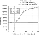
ここで、短絡時における半導体装置1の電界強度について、図4を参照しつつ説明する。なお、図4は、図5に示されるように、半導体装置1を電源30にコイル40を介して接続した状態で短絡評価を行った際のシミュレーション結果を示す図である。また、図4は、FS層20を2.0×1012cm-2のドーズ量で構成し、コレクタ層21を3.56×1012cm-2のドーズ量で構成し、FS層20とコレクタ層21とのピーク間距離Xを1.5μmとした場合のシミュレーション結果を示す図である。
Here, the electric field strength of the
図4に示されるように、半導体装置1におけるオフ時の電界強度は、ベース層12とドリフト層11との接合部近傍でピークが発生し、コレクタ層21側に向かって徐々に小さくなる。一方、半導体装置1における短絡時の電界強度は、ベース層12とドリフト層11との接合部近傍よりも下部電極22側であるFS層20内でピークが発生している。このように、短絡時において、電界強度のピークがFS層20内で発生するのは、図6に示されるように、FS層20のうちの電界強度における下部電極22側の端部となる部分に注入される正孔が少なく、電子が過多状態となるためである。そして、半導体装置1は、このように電界強度のピークが下部電極22側で発生すると、アバランシェ降伏が発生して破壊される可能性がある。なお、図6では、正孔をhで示し、電子をeで示している。
As shown in FIG. 4, the electric field strength when the
このため、本発明者らは、短絡時において、FS層20のうちの電界強度のピークと成り得る位置に注入される正孔を増加して電子の過多状態を緩和することにより、電界強度のピークが下部電極22側で発生し難くなると考えた。そして、本発明者らは、まず、FS層20のうちの電界強度のピークと成り得る位置に注入される正孔が増加するように、コレクタ層21のキャリア濃度を高くして同様のシミュレーションを行い、図7に示す結果を得た。なお、図7は、FS層20を2.0×1012cm-2のドーズ量で構成し、コレクタ層を1.65×1013cm-2のドーズ量で構成し、FS層20とコレクタ層21とのピーク間距離Xを1.5μmとした場合のシミュレーション結果を示す図である。
Therefore, the present inventors increase the number of holes injected into the position of the
図7に示されるように、コレクタ層21を高キャリア濃度にしても、半導体装置1におけるオフ時の電界強度はほとんど変化しない。一方、半導体装置1における短絡時の電界強度は、FS層20内にピークが発生しておらず、ベース層12とドリフト層11との接合部近傍がピークとなっていることが確認される。このように、電界強度のピークがFS層20内で発生し難くなるのは、図8に示されるように、コレクタ層21のキャリア濃度を高くすることにより、FS層20のうちの電界強度のピークと成り得る位置に注入される正孔が増加して電子の過多状態が緩和されるためである。なお、図8では、正孔をhで示し、電子をeで示している。
As shown in FIG. 7, even if the
以上より、短絡時において、電界強度のピークが下部電極22側で発生し難いようにするためには、FS層20のうちの電界強度のピークと成り得る位置に注入される正孔を増加させればよいことになる。なお、短絡時において、FS層20のうちの電界強度のピークと成り得る位置は、FS層20のキャリア濃度およびFS層20のキャリア濃度の最大ピーク位置に依存する。また、FS層20のうちの電界強度のピークと成り得る位置に注入される正孔の量は、コレクタ層21のキャリア濃度、およびFS層20とコレクタ層21とのピーク間距離Xに依存する。
From the above, in order to prevent the peak of the electric field strength from occurring on the
このため、本発明者らは、FS層20のキャリア濃度、コレクタ層21のキャリア濃度、FS層20とコレクタ層21とのピーク間距離Xについてさらに詳細な検討を行った。言い換えると、本発明者らは、FS層20を構成するドーズ量、コレクタ層21を構成するドーズ量、FS層20とコレクタ層21とのピーク間距離Xについてさらに詳細な検討を行った。そして、本発明者らは、図9A~図9Cに示されるシミュレーション結果を得た。
Therefore, the present inventors have conducted a more detailed study on the carrier concentration of the
なお、図9A~図9Cは、コレクタ層21を構成するドーズ量を3.82×1012cm-2で一定とし、FS層20を構成するドーズ量を変化させた場合の図である。つまり、図9A~図9Cは、コレクタ層21のキャリア濃度を一定とし、FS層20のキャリア濃度を変化させた場合の図である。また、図9A~図9Cは、電源電圧を757V、ゲート電極15に印加される電圧を16Vとしたシミュレーション結果であって、短絡時の下部電極22側の電界強度を示している。以下では、短絡時の下部電極22側の電界強度を単に下部の電界強度ともいう。
9A to 9C are views in the case where the dose amount constituting the
さらに、図9A~図9Cにおいて、第1~第4位置は、FS層20におけるキャリア濃度のピークの位置を示しており、第1位置が他面10b側に最も近く、第2、第3、第4位置の順に他面10bから離れた位置となっている。さらに、図9A~図9C中の不純物総量比Yは、FS層20を構成するドーズ量に対するコレクタ層21を構成するドーズ量の比である。但し、FS層20のキャリア濃度は、FS層20を構成するドーズ量に依存し、コレクタ層21のキャリア濃度は、コレクタ層21を構成するドーズ量に依存する。このため、不純物総量比Yは、FS層20のキャリア濃度に対するコレクタ層21のキャリア濃度の比ということもできる。
Further, in FIGS. 9A to 9C, the first to fourth positions indicate the positions of the peaks of the carrier concentration in the
図9A~図9Cに示されるように、第1~第4位置における各プロットを用いて導出される近似曲線は、同じであることが確認される。つまり、下部の電界強度は、FS層20におけるキャリア濃度のピーク位置には依存せず、FS層20とコレクタ層21とのピーク間距離Xに依存することが確認される。すなわち、下部の電界強度は、FS20とコレクタ層21とのピーク間距離Xが等しければ、FS層20におけるキャリア濃度のピーク位置が異なっていても同じとなる。
As shown in FIGS. 9A-9C, it is confirmed that the approximate curves derived using each plot at the first to fourth positions are the same. That is, it is confirmed that the electric field strength at the lower part does not depend on the peak position of the carrier concentration in the
そして、図9Aに示されるように、半導体装置1は、FS層20を構成する際のドーズ量が4×1012cm-2である場合、つまり不純物総量比Yが0.955の場合には、ピーク間距離Xが0.4μm以上になると下部の電界強度が上昇し始める。なお、下部の電界強度が上昇し始めるとは、短絡時にアバランシェ降伏が発生し易くなることである。
Then, as shown in FIG. 9A, the
同様に、図9Bに示されるように、半導体装置1は、FS層20を構成する際のドーズ量が2×1012cm-2である場合、つまり不純物総量比Yが1.910の場合には、ピーク間距離Xが1.2μm以上になると下部の電界強度が上昇し始める。
Similarly, as shown in FIG. 9B, the
さらに、図9Cに示されるように、半導体装置1は、FS層20を構成する際のドーズ量が1×1012cm-2である場合、つまり不純物総量比Yが3.820の場合には、ピーク間距離Xが1.8μm以上になると下部の電界強度が上昇し始める。
Further, as shown in FIG. 9C, the
また、本発明者らは、FS層20を構成するドーズ量およびコレクタ層21を構成するドーズ量を変化させて同様のシミュレーションを行い、図10Aおよび図10Bに示す結果を得た。
Further, the present inventors performed the same simulation by changing the dose amount constituting the
すなわち、図10Aに示されるように、半導体装置1は、FS層20を構成する際のドーズ量が2×1012cm-2であり、コレクタ層21を構成する際のドーズ量が5.22×1012cm-2である場合、ピーク間距離Xが0.7μm以上になると下部の電界強度が上昇し始める。つまり、半導体装置1は、不純物総量比Yが1.305である場合、ピーク間距離Xが0.7μm以上になると下部の電界強度が上昇し始める。
That is, as shown in FIG. 10A, the
また、図10Bに示されるように、半導体装置1は、FS層20を構成する際のドーズ量が1×1012cm-2であり、コレクタ層21を構成する際のドーズ量が3.12×1012cm-2である場合、ピーク間距離Xが1.7μm以上になると下部の電界強度が上昇し始める。つまり、半導体装置1は、不純物総量比Yが3.120である場合、ピーク間距離Xが1.7μm以上になると下部の電界強度が上昇し始める。
Further, as shown in FIG. 10B, in the
以上より、下部の電界強度は、不純物総量比Yと、FS層20とコレクタ層21とのピーク間距離Xとに依存することが確認される。そして、上記図9A~図9C、図10A、および図10Bを用いて不純物総量比YとFS層20とコレクタ層21とのピーク間距離Xとの関係について纏めると、図11に示されるようになる。なお、図11は、図9A~図9C、図10Aおよび図10Bにおける各不純物総量比Yの下部の電界強度が上昇し始めるFS層20とコレクタ層21とのピーク間距離Xをプロットした図である。
From the above, it is confirmed that the electric field strength at the lower part depends on the total impurity ratio Y and the inter-peak distance X between the
図11に示されるように、半導体装置1は、FS層20とコレクタ層21とのピーク間距離をX[μm]、不純物総量比をYとすると、Y≧0.69X2+0.08X+0.86を満たせば、下部の電界強度が増加することを抑制できることが確認される。このため、本実施形態では、FS層20およびコレクタ層21は、Y≧0.69X2+0.08X+0.86を満たすように形成されている。これにより、下部の電界強度が高くなることを抑制でき、短絡耐量を向上できる。
As shown in FIG. 11, in the
なお、FS層20およびコレクタ層21は、Y≧0.69X2+0.08X+0.86を満たす範囲で形成されれば短絡耐量を向上できるが、不純物総量比Yを高くし過ぎると、テール電流によってスイッチング速度が低下する可能性がある。このため、不純物総量比Yは、用途に応じて適宜設計されることが好ましく、例えば、スイッチング速度が重要視される場合には、0.69X2+0.08X+0.86で設定される値の近傍の値とされることが好ましい。これによれば、スイッチング速度が低下することを抑制しつつ、短絡耐量の向上を図ることができる。
If the
また、上記のように、FS層20とコレクタ層21とのピーク間距離Xおよび不純物総量比Yを選択する場合、コレクタ層21は、他面10bを構成する部分のキャリア濃度が1×1016cm-3以上となるようにされることが好ましい。これにより、コレクタ層21を下部電極22とオーミック接触された状態とできる。
Further, as described above, when the peak-to-peak distance X between the
以上説明したように、本実施形態では、FS層20およびコレクタ層21は、Y≧0.69X2+0.08X+0.86を満たすように形成されている。このため、短絡時において、下部の電界強度が高くなることを抑制でき、短絡耐量の向上を図ることができる。
As described above, in the present embodiment, the
(第2実施形態)
第2実施形態について説明する。第2実施形態は、第1実施形態に対し、コレクタ層21におけるキャリア濃度の分布を変更したものである。その他に関しては、第1実施形態と同様であるため、ここでは説明を省略する。
(Second Embodiment)
The second embodiment will be described. The second embodiment is a modification of the first embodiment in which the distribution of the carrier concentration in the
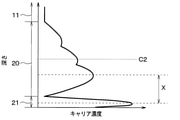
本実施形態の半導体装置1は、基本的な構成は上記第1実施形態と同様である。そして、本実施形態では、コレクタ層21は、図12に示されるように、キャリア濃度が複数のピークを有するように構成されている。具体的には、コレクタ層21とFS層20との積層方向を厚さ方向とすると、コレクタ層21は、厚さ方向において、キャリア濃度の最大ピーク位置が中心C1よりもドリフト層11側に位置するように形成されている。また、コレクタ層21は、厚さ方向において、キャリア濃度における最大ピークよりも小さい補助ピークが中心C1よりも他面10b側に位置するように形成されている。つまり、コレクタ層21は、厚さ方向における中心C1を基準として、キャリア濃度の分布が非対称となるように形成されている。
The
なお、このようなコレクタ層21は、例えば、加速電圧を変更した複数回のイオン注入を行うことによって形成される。
It should be noted that such a
以上説明したように、本実施形態では、コレクタ層21は、キャリア濃度の最大ピーク位置が中心C1よりもドリフト層11側に位置するように形成されている。このため、半導体装置1では、FS層20とコレクタ層21とのピーク間距離Xを短くし易くなる。したがって、例えば、コレクタ層21におけるキャリア濃度の最大ピーク位置が中心C1よりも他面10b側に位置している場合と比較して、FS層20のうちの電界強度のピークと成り得る位置に注入される正孔を増加し易くなり、短絡耐量の向上を図ることができる。
As described above, in the present embodiment, the
また、コレクタ層21は、当該コレクタ層21の中心C1より他面側に補助ピークを有するように形成されている。このため、コレクタ層21を他面10bから深くまで形成しても、コレクタ層21における他面10bを構成する部分のキャリア濃度を1.0×1016cm-3以上とし易くできる。また、コレクタ層21を他面10bから深くまで形成し易くできるため、FS層20とコレクタ層21との界面を他面10bから深い位置にし易くできる。つまり、FS層20と他面10bとの間隔を長くし易くできる。
Further, the
ここで、上記のような半導体装置1は、所定の製造プロセスが行われることによって製造され、製造プロセスにおいて、例えば、半導体基板10が他面10b側から研削等して薄くされたり、搬送等されたりする。この場合、半導体基板10の他面10b側に傷が導入される可能性がある。そして、FS層20が形成されている場合にFS層20に傷が達する、またはFS層20が形成される前にFS層20が形成される部分まで傷が達すると、当該傷によって半導体装置1の耐圧が変化してしまう。つまり、半導体装置1の特性が変化してしまう。特に、オフ時において、空乏層の端部が位置する部分まで傷が達してしまった場合には、半導体装置1の特性が大きく変化してしまう。
Here, the
しかしながら、本実施形態では、上記のようにコレクタ層21を形成することにより、FS層20と他面10bとの間隔を長くし易くできる。このため、本実施形態の半導体装置1では、FS層20に傷が達し難い構成とできる。したがって、本実施形態では、半導体装置1の特性が変化することも抑制できる。言い換えると、本実施形態では、半導体装置1の良品効率の向上を図ることができる。
However, in the present embodiment, by forming the
(第3実施形態)
第3実施形態について説明する。第3実施形態は、第1実施形態に対し、FS層20におけるキャリア濃度の分布を変更したものである。その他に関しては、第1実施形態と同様であるため、ここでは説明を省略する。
(Third Embodiment)
The third embodiment will be described. The third embodiment is a modification of the first embodiment in which the distribution of the carrier concentration in the
本実施形態の半導体装置1は、基本的な構成は上記第1実施形態と同様である。そして、本実施形態では、FS層20は、図13に示されるように、キャリア濃度が複数のピークを有するように構成されている。具体的には、FS層20は、厚さ方向において、キャリア濃度の最大ピーク位置が中心C2よりもドリフト層11側に位置するように形成されている。
The
これによれば、FS層20は、最大ピーク位置が当該FS層20の中心C2よりもドリフト層11側に位置している。このため、例えば、最大ピーク位置が当該FS層20の中心C2に位置している場合と比較して、空乏層の端部をドリフト層11側に位置させることができる。したがって、傷が空乏層の端部となる位置まで達し難くなり、半導体装置1の特性が変化することを抑制できる。
According to this, the maximum peak position of the
(第4実施形態)
第4実施形態について説明する。第4実施形態は、第1実施形態に対し、FS層20におけるキャリア濃度の分布を変更したものである。その他に関しては、第1実施形態と同様であるため、ここでは説明を省略する。
(Fourth Embodiment)
The fourth embodiment will be described. The fourth embodiment is a modification of the first embodiment in which the distribution of the carrier concentration in the
本実施形態の半導体装置1は、基本的な構成は上記第1実施形態と同様である。そして、本実施形態では、FS層20は、図14に示されるように、キャリア濃度が複数のピークを有するように構成されている。具体的には、FS層20は、厚さ方向において、キャリア濃度の最大ピーク位置が中心C2よりもコレクタ層21側に位置するように形成されている。
The
これによれば、FS層20は、最大ピーク位置が当該FS層20の中心C2よりもコレクタ層21側に位置している。このため、例えば、最大ピーク位置が当該FS層20の中心C2に位置している場合と比較して、FS層20とコレクタ層21とのピーク間距離Xを短くし易くできる。したがって、短絡耐量の向上を図り易くなる。
According to this, the maximum peak position of the
(他の実施形態)
本発明は上記した実施形態に限定されるものではなく、特許請求の範囲に記載した範囲内において適宜変更が可能である。
(Other embodiments)
The present invention is not limited to the above-described embodiment, and can be appropriately modified within the scope of the claims.
例えば、上記各実施形態は、第1導電型がP型であり、第2導電型がN型とされていてもよい。 For example, in each of the above embodiments, the first conductive type may be P type and the second conductive type may be N type.
また、上記各実施形態は、半導体基板10の他面10b側にN型のカソード層が形成されたRC(Reverse-Conductingの略)-IGBTに適用されてもよい。
Further, each of the above embodiments may be applied to an RC (abbreviation of Reverse-Conducting) -IGBT in which an N-type cathode layer is formed on the
さらに、上記各実施形態は、トレンチ13が形成されておらず、ゲート電極15が半導体基板10の一面10a上に形成されていてもよい。すなわち、上記各実施形態は、プレーナ型の半導体装置1に適用することもできる。
Further, in each of the above embodiments, the
また、上記第2実施形態において、図15に示されるように、コレクタ層21は、キャリア濃度の分布において、最大ピークよりも小さい補助ピークを複数有する構成とされていてもよい。さらに、上記第2実施形態において、コレクタ層21は、補助ピークを有しない構成とされていてもよい。
Further, in the second embodiment, as shown in FIG. 15, the
そして、上記各実施形態を適宜組み合わせてもよい。例えば、上記第2実施形態を上記第3、第4実施形態に組み合わせ、コレクタ層21のキャリア濃度が複数のピークを有するように構成されていてもよい。
Then, each of the above-described embodiments may be combined as appropriate. For example, the second embodiment may be combined with the third and fourth embodiments so that the carrier concentration of the
10 半導体基板
11 ドリフト層
12 ベース層
14 ゲート絶縁膜
15 ゲート電極
16 エミッタ領域
19 第1電極
22 第2電極
10
Claims (4)
第1導電型のドリフト層(11)と、
前記ドリフト層上に形成された第2導電型のベース層(12)と、
前記ベース層の表層部に形成された第1導電型のエミッタ領域(16)と、
前記ベース層のうちの前記ドリフト層と前記エミッタ領域との間に形成されたゲート絶縁膜(14)と、
前記ゲート絶縁膜上に形成されたゲート電極(15)と、
前記ドリフト層のうちの前記ベース層側と反対側に形成された第2導電型のコレクタ層(21)と、
前記コレクタ層と前記ドリフト層との間に形成され、前記ドリフト層よりも高キャリア濃度とされた第1導電型の前記フィールドストップ層と、
前記ベース層および前記エミッタ領域と電気的に接続される第1電極(19)と、
前記コレクタ層と電気的に接続される第2電極(22)と、を備え、
前記フィールドストップ層および前記コレクタ層は、前記フィールドストップ層におけるキャリア濃度が最大となる最大ピーク位置と前記コレクタ層におけるキャリア濃度が最大となる最大ピーク位置との間の距離をX[μm]、前記フィールドストップ層を構成するドーズ量に対する前記コレクタ層を構成するドーズ量の比である不純物総量比をYとすると、Y≧0.69X2+0.08X+0.86を満たす構成とされており、
前記コレクタ層は、前記コレクタ層と前記フィールドストップ層との積層方向において、前記コレクタ層の最大ピーク位置が当該コレクタ層の中心(C1)より前記ドリフト層側に位置している半導体装置。 A semiconductor device having a field stop layer (20).
The first conductive type drift layer (11) and
The second conductive type base layer (12) formed on the drift layer and
The first conductive type emitter region (16) formed on the surface layer of the base layer and
A gate insulating film (14) formed between the drift layer and the emitter region of the base layer,
The gate electrode (15) formed on the gate insulating film and the gate electrode (15)
A second conductive type collector layer (21) formed on the side of the drift layer opposite to the base layer side, and
The first conductive type field stop layer formed between the collector layer and the drift layer and having a higher carrier concentration than the drift layer,
A first electrode (19) electrically connected to the base layer and the emitter region,
A second electrode (22) electrically connected to the collector layer is provided.
The field stop layer and the collector layer have a distance of X [μm] between the maximum peak position where the carrier concentration in the field stop layer is maximum and the maximum peak position where the carrier concentration is maximum in the collector layer. Assuming that the total amount of impurities ratio, which is the ratio of the dose amount constituting the collector layer to the dose amount constituting the field stop layer, is Y, the configuration satisfies Y ≧ 0.69X2 + 0.08X + 0.86 .
The collector layer is a semiconductor device in which the maximum peak position of the collector layer is located closer to the drift layer than the center (C1) of the collector layer in the stacking direction of the collector layer and the field stop layer .
Priority Applications (4)
| Application Number | Priority Date | Filing Date | Title |
|---|---|---|---|
| JP2018171732A JP7010184B2 (en) | 2018-09-13 | 2018-09-13 | Semiconductor device |
| PCT/JP2019/033934 WO2020054446A1 (en) | 2018-09-13 | 2019-08-29 | Semiconductor device |
| CN201980059059.9A CN112689902B (en) | 2018-09-13 | 2019-08-29 | Semiconductor device with a semiconductor device having a plurality of semiconductor chips |
| US17/198,807 US20210217845A1 (en) | 2018-09-13 | 2021-03-11 | Semiconductor device |
Applications Claiming Priority (1)
| Application Number | Priority Date | Filing Date | Title |
|---|---|---|---|
| JP2018171732A JP7010184B2 (en) | 2018-09-13 | 2018-09-13 | Semiconductor device |
Publications (3)
| Publication Number | Publication Date |
|---|---|
| JP2020043301A JP2020043301A (en) | 2020-03-19 |
| JP2020043301A5 JP2020043301A5 (en) | 2021-01-28 |
| JP7010184B2 true JP7010184B2 (en) | 2022-01-26 |
Family
ID=69778270
Family Applications (1)
| Application Number | Title | Priority Date | Filing Date |
|---|---|---|---|
| JP2018171732A Active JP7010184B2 (en) | 2018-09-13 | 2018-09-13 | Semiconductor device |
Country Status (3)
| Country | Link |
|---|---|
| US (1) | US20210217845A1 (en) |
| JP (1) | JP7010184B2 (en) |
| WO (1) | WO2020054446A1 (en) |
Families Citing this family (3)
| Publication number | Priority date | Publication date | Assignee | Title |
|---|---|---|---|---|
| CN113644123B (en) * | 2021-06-28 | 2024-09-06 | 华为技术有限公司 | Semiconductor device and related chip and preparation method |
| JP2024064037A (en) * | 2022-10-27 | 2024-05-14 | 株式会社デンソー | Semiconductor Device |
| JP2024080317A (en) * | 2022-12-02 | 2024-06-13 | 株式会社デンソー | Semiconductor device and manufacturing method for the same |
Citations (3)
| Publication number | Priority date | Publication date | Assignee | Title |
|---|---|---|---|---|
| US20080001257A1 (en) | 2006-06-30 | 2008-01-03 | Infineon Technologies Austria Ag | Semiconductor device with a field stop zone |
| JP2012156207A (en) | 2011-01-24 | 2012-08-16 | Mitsubishi Electric Corp | Semiconductor device and method of manufacturing the same |
| WO2016204126A1 (en) | 2015-06-17 | 2016-12-22 | 富士電機株式会社 | Semiconductor device |
Family Cites Families (2)
| Publication number | Priority date | Publication date | Assignee | Title |
|---|---|---|---|---|
| US5763915A (en) * | 1996-02-27 | 1998-06-09 | Magemos Corporation | DMOS transistors having trenched gate oxide |
| DE112010005443B4 (en) * | 2010-04-02 | 2019-03-14 | Toyota Jidosha Kabushiki Kaisha | Semiconductor device having a semiconductor substrate with a diode region and an IGBT region and method for its production |
-
2018
- 2018-09-13 JP JP2018171732A patent/JP7010184B2/en active Active
-
2019
- 2019-08-29 WO PCT/JP2019/033934 patent/WO2020054446A1/en active Application Filing
-
2021
- 2021-03-11 US US17/198,807 patent/US20210217845A1/en active Pending
Patent Citations (3)
| Publication number | Priority date | Publication date | Assignee | Title |
|---|---|---|---|---|
| US20080001257A1 (en) | 2006-06-30 | 2008-01-03 | Infineon Technologies Austria Ag | Semiconductor device with a field stop zone |
| JP2012156207A (en) | 2011-01-24 | 2012-08-16 | Mitsubishi Electric Corp | Semiconductor device and method of manufacturing the same |
| WO2016204126A1 (en) | 2015-06-17 | 2016-12-22 | 富士電機株式会社 | Semiconductor device |
Also Published As
| Publication number | Publication date |
|---|---|
| CN112689902A (en) | 2021-04-20 |
| WO2020054446A1 (en) | 2020-03-19 |
| US20210217845A1 (en) | 2021-07-15 |
| JP2020043301A (en) | 2020-03-19 |
Similar Documents
| Publication | Publication Date | Title |
|---|---|---|
| US9153676B2 (en) | Insulated gate bipolar transistor | |
| US8975690B2 (en) | Semiconductor device | |
| JP5985624B2 (en) | Insulated gate transistor and method of manufacturing the same | |
| JP5865618B2 (en) | Semiconductor device | |
| TWI575736B (en) | Dual trench-gate igbt structure | |
| KR101701667B1 (en) | Igbt using trench gate electrode | |
| JP6356803B2 (en) | Insulated gate bipolar transistor | |
| US20210217845A1 (en) | Semiconductor device | |
| US11075285B2 (en) | Insulated gate power semiconductor device and method for manufacturing such a device | |
| JP6571467B2 (en) | Insulated gate type switching element and manufacturing method thereof | |
| JP5200373B2 (en) | Semiconductor device | |
| JPWO2016042955A1 (en) | Semiconductor device and manufacturing method of semiconductor device | |
| CN108365007B (en) | Insulated gate bipolar transistor | |
| JP5838176B2 (en) | Semiconductor device | |
| WO2021220965A1 (en) | Semiconductor device | |
| JP2006332591A (en) | Semiconductor device | |
| US11264475B2 (en) | Semiconductor device having a gate electrode formed in a trench structure | |
| JP2017191817A (en) | Method for manufacturing switching element | |
| US20150171198A1 (en) | Power semiconductor device | |
| JP2019117867A (en) | Semiconductor device | |
| KR20150061201A (en) | Power semiconductor device and method of fabricating the same | |
| CN108305893B (en) | Semiconductor device with a plurality of semiconductor chips | |
| US20150144993A1 (en) | Power semiconductor device | |
| JP2017045874A (en) | Semiconductor device | |
| JP2018125326A (en) | Semiconductor device |
Legal Events
| Date | Code | Title | Description |
|---|---|---|---|
| A711 | Notification of change in applicant |
Free format text: JAPANESE INTERMEDIATE CODE: A711 Effective date: 20201030 |
|
| A521 | Request for written amendment filed |
Free format text: JAPANESE INTERMEDIATE CODE: A821 Effective date: 20201030 |
|
| A521 | Request for written amendment filed |
Free format text: JAPANESE INTERMEDIATE CODE: A523 Effective date: 20201209 |
|
| A621 | Written request for application examination |
Free format text: JAPANESE INTERMEDIATE CODE: A621 Effective date: 20210217 |
|
| TRDD | Decision of grant or rejection written | ||
| A01 | Written decision to grant a patent or to grant a registration (utility model) |
Free format text: JAPANESE INTERMEDIATE CODE: A01 Effective date: 20211214 |
|
| A61 | First payment of annual fees (during grant procedure) |
Free format text: JAPANESE INTERMEDIATE CODE: A61 Effective date: 20211227 |