JP2017191817A - Method for manufacturing switching element - Google Patents
Method for manufacturing switching element Download PDFInfo
- Publication number
- JP2017191817A JP2017191817A JP2016078925A JP2016078925A JP2017191817A JP 2017191817 A JP2017191817 A JP 2017191817A JP 2016078925 A JP2016078925 A JP 2016078925A JP 2016078925 A JP2016078925 A JP 2016078925A JP 2017191817 A JP2017191817 A JP 2017191817A
- Authority
- JP
- Japan
- Prior art keywords
- region
- trench
- mask
- insulating layer
- type
- Prior art date
- Legal status (The legal status is an assumption and is not a legal conclusion. Google has not performed a legal analysis and makes no representation as to the accuracy of the status listed.)
- Pending
Links
Images
Landscapes
- Electrodes Of Semiconductors (AREA)
Abstract
Description
本明細書が開示する技術は、スイッチング素子の製造方法に関する。 The technology disclosed in this specification relates to a method for manufacturing a switching element.
特許文献1には、トレンチ内に配置されたゲート電極を備えるスイッチング素子が開示されている。このスイッチング素子は、n型のソース領域とp型のボディ領域とn型のドリフト領域を有する。ソース領域は、トレンチの側面においてゲート絶縁層に接している。ボディ領域は、トレンチの側面においてソース領域の下側でゲート絶縁層に接している。ドリフト領域は、トレンチの側面においてボディ領域の下側でゲート絶縁層に接している。また、このスイッチング素子は、p型の接続領域とp型の底部領域を有している。底部領域は、トレンチの底面においてゲート絶縁層に接している。接続領域は、トレンチの短手方向の側面(トレンチの短手方向の端部に位置する側面)の一部に設けられている。接続領域は、短手方向の側面に沿ってボディ領域から下側に伸びている。接続領域によって、底部領域とボディ領域とが接続されている。上述したドリフト領域は、短手方向の側面のうちの接続領域が存在しない範囲でゲート絶縁層に接している。 Patent Document 1 discloses a switching element including a gate electrode arranged in a trench. This switching element has an n-type source region, a p-type body region, and an n-type drift region. The source region is in contact with the gate insulating layer on the side surface of the trench. The body region is in contact with the gate insulating layer below the source region on the side surface of the trench. The drift region is in contact with the gate insulating layer below the body region on the side surface of the trench. The switching element has a p-type connection region and a p-type bottom region. The bottom region is in contact with the gate insulating layer at the bottom of the trench. The connection region is provided on a part of the lateral side surface of the trench (side surface located at the end portion of the trench in the lateral direction). The connection region extends downward from the body region along the lateral side surface. The bottom region and the body region are connected by the connection region. The above-described drift region is in contact with the gate insulating layer in a range where no connection region exists in the side surface in the short direction.
このスイッチング素子がオフするときには、底部領域からドリフト領域に空乏層が伸びる。この空乏層によって、底部領域の近傍(すなわち、トレンチの底部近傍)における電界集中が抑制される。このスイッチング素子がオンするときには、接続領域を介してボディ領域から底部領域にホールが供給される。底部領域にホールが供給されると、底部領域からドリフト領域に広がっていた空乏層が底部領域に向かって収縮して消滅する。このため、スイッチング素子がオンするときに短時間でドリフト領域の抵抗が低下する。したがって、このスイッチング素子では、損失が生じ難い。 When the switching element is turned off, a depletion layer extends from the bottom region to the drift region. This depletion layer suppresses electric field concentration in the vicinity of the bottom region (that is, in the vicinity of the bottom of the trench). When this switching element is turned on, holes are supplied from the body region to the bottom region via the connection region. When holes are supplied to the bottom region, the depletion layer that has spread from the bottom region to the drift region contracts toward the bottom region and disappears. For this reason, the resistance of the drift region decreases in a short time when the switching element is turned on. Therefore, in this switching element, it is difficult for loss to occur.
特許文献1のスイッチング素子のようにトレンチの短手方向の側面の一部に設けられたp型の接続領域は、従来は、以下のようにして形成される。まず、トレンチの短手方向の側面を部分的に覆うマスクが形成される。ここでは、接続領域を形成しない範囲にマスクが形成される。次に、トレンチの深さ方向に対して傾斜した方向に沿った不純物照射によって、マスクに覆われていない範囲の短手方向の側面にp型不純物が注入される。これによって、短手方向の側面に露出する範囲に、部分的に、接続領域が形成される。その後、マスクがエッチングにより除去される。 Conventionally, a p-type connection region provided on a part of a lateral surface of a trench as in the switching element of Patent Document 1 is formed as follows. First, a mask that partially covers the lateral side surface of the trench is formed. Here, the mask is formed in a range where the connection region is not formed. Next, p-type impurities are implanted into the lateral side surface in the range not covered by the mask by impurity irradiation along the direction inclined with respect to the depth direction of the trench. As a result, a connection region is partially formed in a range exposed on the side surface in the short direction. Thereafter, the mask is removed by etching.
上記の製造方法では、トレンチの短手方向の側面にp型不純物を注入する際に、マスクにもp型不純物が注入される。マスクへのp型不純物の注入によって、マスクの一部が変質する場合がある。すると、その後にマスクをエッチングするときに、マスクの変質部を除去できず、トレンチの側面にマスクの変質部が残存する場合がある。このため、スイッチング素子の製造歩留まりが低下するという問題がある。 In the above manufacturing method, when the p-type impurity is implanted into the lateral side surface of the trench, the p-type impurity is also implanted into the mask. A portion of the mask may be altered due to the implantation of p-type impurities into the mask. Then, when the mask is subsequently etched, the altered portion of the mask may not be removed, and the altered portion of the mask may remain on the side surface of the trench. For this reason, there exists a problem that the manufacturing yield of a switching element falls.
本明細書が開示する製造方法により製造されるスイッチング素子は、半導体基板と、前記半導体基板の上面に設けられたトレンチと、前記トレンチの内面を覆っているゲート絶縁層と、前記トレンチ内に配置されているとともに前記ゲート絶縁層によって前記半導体基板から絶縁されているゲート電極を有している。前記半導体基板は、ソース領域と、ボディ領域と、第1接続領域と、第2接続領域と、ドリフト領域と、底部領域を有している。前記ソース領域は、前記トレンチの短手方向の端部に位置する第1側面において前記ゲート絶縁層に接しているn型の領域である。前記ボディ領域は、前記第1側面において前記ソース領域の下側で前記ゲート絶縁層に接しており、前記トレンチの長手方向の端部に位置する第2側面において前記ゲート絶縁層に接しているp型の領域である。前記第1接続領域は、前記第1側面に沿って前記ボディ領域から下側に伸びているp型の領域である。前記第2接続領域は、前記第2側面に沿って前記ボディ領域から下側に伸びているp型の領域である。前記ドリフト領域は、前記ボディ領域の下側の前記第1側面の前記第1接続領域が存在しない範囲において前記ゲート絶縁層に接しており、前記ボディ領域によって前記ソース領域から分離されているn型の領域である。前記底部領域は、前記トレンチの底面において前記ゲート絶縁層に接しており、前記第1接続領域と前記第2接続領域に接続されているp型の領域である。本明細書が開示する製造方法は、前記トレンチを形成する工程と、前記第1側面に犠牲酸化膜を形成する工程と、前記犠牲酸化膜の表面に、前記第1側面の一部を覆うマスクを形成する工程と、前記トレンチの深さ方向に対して傾斜した方向に沿った不純物照射によって前記マスクに覆われていない範囲の前記第1側面にp型不純物を注入する工程と、前記マスクをエッチングにより除去する工程と、前記犠牲酸化膜をエッチングにより除去する工程を有する。 A switching element manufactured by the manufacturing method disclosed in this specification includes a semiconductor substrate, a trench provided on an upper surface of the semiconductor substrate, a gate insulating layer covering an inner surface of the trench, and the trench. And a gate electrode insulated from the semiconductor substrate by the gate insulating layer. The semiconductor substrate has a source region, a body region, a first connection region, a second connection region, a drift region, and a bottom region. The source region is an n-type region in contact with the gate insulating layer on a first side surface located at an end portion in the short direction of the trench. The body region is in contact with the gate insulating layer on the lower side of the source region on the first side surface, and is in contact with the gate insulating layer on a second side surface located at an end in the longitudinal direction of the trench. It is an area of a type. The first connection region is a p-type region extending downward from the body region along the first side surface. The second connection region is a p-type region extending downward from the body region along the second side surface. The drift region is in contact with the gate insulating layer in a range where the first connection region on the first side surface below the body region does not exist, and is separated from the source region by the body region It is an area. The bottom region is a p-type region that is in contact with the gate insulating layer at the bottom surface of the trench and is connected to the first connection region and the second connection region. The manufacturing method disclosed in the present specification includes a step of forming the trench, a step of forming a sacrificial oxide film on the first side surface, and a mask that covers a part of the first side surface on the surface of the sacrificial oxide film. Forming a p-type impurity into the first side surface in a range not covered by the mask by impurity irradiation along a direction inclined with respect to the depth direction of the trench; and A step of removing by etching, and a step of removing the sacrificial oxide film by etching.
この製造方法では、第1側面に犠牲酸化膜を形成し、その犠牲酸化膜の表面にマスクを形成する。その後の不純物照射によってマスクに覆われていない範囲の第1側面にp型不純物が注入され、その注入範囲に第1接続領域が形成される。また、不純物照射によって、マスクが変質する場合がある。この場合、その後にマスクをエッチングする際に、マスクの変質部が犠牲酸化膜の表面に残存する。しかしながら、このようにマスクの変質部が残存した場合でも、その後の犠牲酸化膜をエッチングする工程において、犠牲酸化膜と共にマスクの変質部も除去される。この製造方法によれば、第1側面にマスクの変質部が残存することを防止することができる。 In this manufacturing method, a sacrificial oxide film is formed on the first side surface, and a mask is formed on the surface of the sacrificial oxide film. A p-type impurity is implanted into the first side surface in a range not covered by the mask by subsequent impurity irradiation, and a first connection region is formed in the implantation range. Further, the mask may be altered by the impurity irradiation. In this case, when the mask is subsequently etched, the altered portion of the mask remains on the surface of the sacrificial oxide film. However, even when the altered portion of the mask remains in this manner, the altered portion of the mask is removed together with the sacrificial oxide film in the subsequent etching process of the sacrificial oxide film. According to this manufacturing method, it is possible to prevent the altered portion of the mask from remaining on the first side surface.
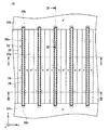
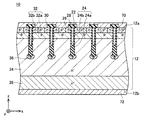
図1〜4は、実施形態のMOSFET10を示している。図2〜4に示すように、MOSFET10は、半導体基板12と、電極、絶縁層等を備えている。なお、図1では、図の見易さのため、半導体基板12の上面12a上の電極、絶縁層の図示を省略している。以下では、半導体基板12の上面12aと平行な一方向をx方向といい、上面12aに平行でx方向に直交する方向をy方向といい、半導体基板12の厚み方向をz方向という。半導体基板12は、SiC(炭化シリコン)によって構成されている。
1-4 has shown MOSFET10 of embodiment. As shown in FIGS. 2 to 4, the
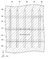
図2、3に示すように、半導体基板12の上面12aには、複数のトレンチ22が設けられている。図1に示すように、各トレンチ22は、y方向に直線状に長く伸びている。複数のトレンチ22は、x方向に間隔を開けて配列されている。図2〜4に示すように、各トレンチ22の内面は、ゲート絶縁層24によって覆われている。ゲート絶縁層24は、底部絶縁層24aと側面絶縁膜24bを有している。底部絶縁層24aは、トレンチ22の底部に配置されている。底部絶縁層24aは、トレンチ22の底面と、トレンチ22の底面近傍の側面を覆っている。底部絶縁層24aは、トレンチ22の深さ方向に厚く形成されている。側面絶縁膜24bは、底部絶縁層24aの上部に位置するトレンチ22の側面を覆っている。各トレンチ22内には、底部絶縁層24aの上部にゲート電極26が配置されている。各ゲート電極26は、ゲート絶縁層24(すなわち、底部絶縁層24aと側面絶縁膜24b)によって半導体基板12から絶縁されている。側面絶縁膜24bの厚み(すなわち、トレンチ22の側面とゲート電極26の側面の間の間隔)は、底部絶縁層24aの厚み(すなわち、ゲート電極26の下端とトレンチ22の底面の間の間隔)よりも薄い。各ゲート電極26の上面は、層間絶縁膜28によって覆われている。
As shown in FIGS. 2 and 3, a plurality of
半導体基板12の上面12aには、上部電極70が配置されている。上部電極70は、層間絶縁膜28が設けられていない部分で半導体基板12の上面12aに接している。上部電極70は、層間絶縁膜28によってゲート電極26から絶縁されている。半導体基板12の下面12bには、下部電極72が配置されている。下部電極72は、半導体基板12の下面12bに接している。
An
図1〜4に示すように、半導体基板12の内部には、複数のソース領域30、ボディ領域32、ドリフト領域34、ドレイン領域35、複数の底部領域36及び複数の接続領域38(38a及び38b)が設けられている。
1-4, the
各ソース領域30は、n型領域である。図1〜3に示すように、各ソース領域30は、半導体基板12の上面12aに露出する位置に配置されており、上部電極70にオーミック接触している。また、各ソース領域30は、トレンチ22の短手方向の側面(短手方向の端部に位置する側面であり、y方向に沿って伸びる側面)において、側面絶縁膜24bに接している。各ソース領域30は、トレンチ22の上端部において、側面絶縁膜24bに接している。
Each
ボディ領域32は、p型領域である。ボディ領域32は、各ソース領域30に接している。ボディ領域32は、2つのソース領域30に挟まれた範囲から各ソース領域30の下側まで伸びている。ボディ領域32は、高濃度領域32aと低濃度領域32bを有している。高濃度領域32aは、低濃度領域32bよりも高いp型不純物濃度を有している。高濃度領域32aは、2つのソース領域30に挟まれた範囲に配置されている。高濃度領域32aは、上部電極70にオーミック接触している。低濃度領域32bは、高濃度領域32aとソース領域30の下側に配置されている。低濃度領域32bは、トレンチ22の短手方向の側面において、側面絶縁膜24bに接している。すなわち、低濃度領域32bは、ソース領域30の下側で、側面絶縁膜24bに接している。また、図1、4に示すように、低濃度領域32bは、トレンチ22の長手方向の側面(長手方向の端部に位置する側面であり、x方向に沿って伸びる側面)に隣接する範囲にも配置されている。低濃度領域32bは、トレンチ22の長手方向の側面において、側面絶縁膜24bに接している。ボディ領域32の下端(すなわち、低濃度領域32bの下端)は、ゲート電極26の下端(すなわち、底部絶縁層24aの上面)よりも上側に配置されている。
ドリフト領域34は、n型領域である。ドリフト領域34は、ボディ領域32の下側に配置されており、ボディ領域32によってソース領域30から分離されている。図2に示すように、ドリフト領域34は、トレンチ22の短手方向の側面において、側面絶縁膜24b及び底部絶縁層24aに接している。すなわち、ドリフト領域34は、ボディ領域32の下側で、側面絶縁膜24b及び底部絶縁層24aに接している。
The
ドレイン領域35は、n型領域である。ドレイン領域35は、ドリフト領域34よりも高いn型不純物濃度を有している。ドレイン領域35は、ドリフト領域34の下側に配置されている。ドレイン領域35は、半導体基板12の下面12bに露出している。ドレイン領域35は、下部電極72にオーミック接触している。
The
各底部領域36は、p型領域である。各底部領域36は、対応するトレンチ22の底面に露出する範囲に配置されている。各底部領域36は、対応するトレンチ22の底面において、底部絶縁層24aに接している。図4に示すように、各底部領域36は、対応するトレンチ22の底面に沿ってy方向に長く伸びている。各底部領域36は、対応するトレンチ22の底面全域で底部絶縁層24aに接している。図2に示すように、各底部領域36の周囲は、ドリフト領域34に囲まれている。後述する接続領域38が形成されている箇所を除いて、各底部領域36は、ドリフト領域34によってボディ領域32から分離されている。
Each
図1に示すように、接続領域38は、トレンチ22の短手方向の側面に沿って設けられている第1接続領域38aと、トレンチ22の長手方向の側面に沿って設けられている第2接続領域38bを有している。図3に示すように、第1接続領域38aは、ボディ領域32からトレンチ22の短手方向の側面に沿って下側に伸びている。図1に示すように、第1接続領域38aは、トレンチ22の短手方向の側面の一部に設けられている。トレンチ22の1つの側面に対して、複数の第1接続領域38aが形成されている。図3に示すように、第1接続領域38aは、トレンチ22の短手方向の側面において、側面絶縁膜24bと底部絶縁層24aに接している。第1接続領域38aの下端は、底部領域36に接続されている。すなわち、第1接続領域38aによって、ボディ領域32と底部領域36が接続されている。図4に示すように、第2接続領域38bは、ボディ領域32からトレンチ22の長手方向の側面に沿って下側に伸びている。第2接続領域38bは、トレンチ22の長手方向の側面において、側面絶縁膜24bと底部絶縁層24aに接している。第2接続領域38bの下端は、底部領域36に接続されている。すなわち、第2接続領域38bによって、ボディ領域32と底部領域36が接続されている。
As shown in FIG. 1, the connection region 38 includes a
次に、MOSFET10の動作について説明する。MOSFET10の使用時には、MOSFET10と負荷(例えば、モータ)と電源が直列に接続される。MOSFET10と負荷の直列回路に対して、電源電圧(本実施形態では、約800V)が印加される。MOSFET10のドレイン側(下部電極72)がソース側(上部電極70)よりも高電位となる向きで、電源電圧が印加される。ゲート電極26にゲートオン電位(ゲート閾値よりも高い電位)を印加すると、側面絶縁膜24bに接する範囲のボディ領域32(低濃度領域32b)にチャネル(反転層)が形成され、MOSFET10がオンする。ゲート電極26にゲートオフ電位(ゲート閾値以下の電位)を印加すると、チャネルが消滅し、MOSFET10がオフする。以下に、MOSFET10のターンオフ時とターンオン時の動作について、詳細に説明する。
Next, the operation of the
MOSFET10をターンオフさせる場合には、ゲート電極26の電位をゲートオン電位からゲートオフ電位に引き下げる。すると、チャネルが消失し、下部電極72の電位が上昇する。下部電極72の電位は、上部電極70に対して電源電圧分(すなわち、約800V)だけ高い電位まで上昇する。下部電極72の電位が上昇する過程において、底部領域36と下部電極72の間の容量結合によって、底部領域36の電位が少し上昇する。すると、底部領域36から接続領域38a、38bとボディ領域32を介して上部電極70へホールが流れる。このようにホールが流れている間は、底部領域36の電位の上昇が抑制され、底部領域36の電位が上部電極70の電位よりもわずかに高い電位に維持される。
When the
また、下部電極72の電位の上昇に伴って、ドレイン領域35及びドリフト領域34の電位も上昇する。ドリフト領域34の電位が上昇すると、ボディ領域32とドリフト領域34の間に電位差が生じる。このため、ボディ領域32とドリフト領域34の界面のpn接合に逆電圧が印加される。したがって、ボディ領域32からドリフト領域34に空乏層が広がる。また、ドリフト領域34の電位が上昇すると、底部領域36とドリフト領域34の間に電位差が生じる。このため、底部領域36とドリフト領域34の界面のpn接合に逆電圧が印加される。したがって、底部領域36からドリフト領域34に空乏層が広がる。このように、ボディ領域32からだけでなく底部領域36からもドリフト領域34に空乏層が広がるので、ドリフト領域34が短時間で空乏化される。さらに、底部領域36から伸びる空乏層によって各トレンチ22の下端部近傍の半導体領域が保護されるので、各トレンチ22の下端部近傍の半導体領域に電界が集中し難い。したがって、MOSFET10は高い耐圧を有する。
As the potential of the
また、ドリフト領域34の電位が上昇すると、接続領域38a、38bとドリフト領域34の界面のpn接合にも逆電圧が印加される。接続領域38a、38bのp型不純物濃度が低いので、pn接合から接続領域38a、38bに広く空乏層が広がる。これによって、接続領域38a、38bが空乏化される。接続領域38a、38bが空乏化されることによって、底部領域36が上部電極70から電気的に分離される。底部領域36がボディ領域32から電気的に分離されると、底部領域36から上部電極70に向かうホールの流れが停止し、底部領域36の電位がフローティングとなる。このため、底部領域36の電位が、下部電極72の電位の上昇に伴って上昇する。このように、底部領域36の電位が上昇することで、底部領域36と下部電極72の間の電位差が過大となることが防止される。下部電極72の電位が上部電極70に対して電源電圧分高い電位まで上昇することで、MOSFET10のターンオフか完了する。
In addition, when the potential of the
MOSFET10をターンオンさせる場合には、ゲート電極26の電位をゲートオフ電位からゲートオン電位に引き上げる。すると、トレンチ22の短手方向の側面において側面絶縁膜24bに接している範囲のボディ領域32(低濃度領域32b)に電子が引き寄せられる。これによって、この範囲のボディ領域32がp型からn型に反転し、チャネルが形成される。チャネルによって、ソース領域30とドリフト領域34が接続される。これによって、ドリフト領域34、ドレイン領域35及び下部電極72の電位が低下する。ドリフト領域34の電位が低下すると、ボディ領域32とドリフト領域34の界面のpn接合に印加されていた逆電圧が低下する。このため、ボディ領域32からドリフト領域34に広がっていた空乏層が、ボディ領域32に向かって収縮し、消滅する。これにより、上部電極70から、ソース領域30、チャネル、ドリフト領域34、ドレイン領域35を経由して下部電極72へ電子が流れるようになる。すなわち、MOSFET10がオンする。
When the
また、ドリフト領域34の電位が低下する過程において、接続領域38a、38bに広がっている空乏層が、ドリフト領域34に向かって収縮し、消滅する。その結果、底部領域36が、接続領域38a、38bを介してボディ領域32に電気的に接続される。すると、上部電極70からボディ領域32と接続領域38を介して底部領域36にホールが流れる。底部領域36にホールが供給されると、底部領域36からドリフト領域34に広がっていた空乏層が底部領域36に向かって収縮し、消滅する。このため、ドリフト領域34の抵抗が低下し、上部電極70から下部電極72に向かって電子が流れ易くなる。なお、底部領域36が抵抗を有するため、接続領域38から底部領域36に供給されたホールが底部領域36全体に行き渡るには一定の時間がかかる。接続領域38の数が少ない場合には、底部領域36のうちの接続領域38から遠い部分にホールが供給されるまでに要する時間が長くなり、その部分の周辺のドリフト領域34で空乏層が消滅するのが遅くなる。これに対し、本実施形態のMOSFET10では、トレンチ22の長手方向の側面に第2接続領域38bが設けられているのに加えて、トレンチ22の短手方向の側面に複数の第1接続領域38aが設けられている。接続領域38a、38bが高密度で形成されているので、接続領域38a、38bから底部領域36にホールが供給されるときに、底部領域36全体にホールが行き渡り易い。したがって、MOSFET10では、ゲート電極26の電位をゲートオン電位に引き上げてから短時間でドリフト領域34の抵抗が低下する。すなわち、このMOSFET10は、ターンオンするときに短時間でオン抵抗が低下する。したがって、このMOSFET10では、損失が生じ難い。
Further, in the process in which the potential of the
次に、実施形態のMOSFET10の製造方法について説明する。まず、加工前の半導体基板12を準備する。加工前の半導体基板12は、ドリフト領域34と略同じn型不純物濃度を有するn型半導体(SiC)によって構成されている。
Next, the manufacturing method of MOSFET10 of embodiment is demonstrated. First, the
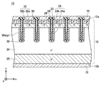
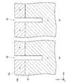
まず、エピタキシャル成長またはイオン注入によって、ボディ領域32の低濃度領域32bを形成する。次に、半導体基板12の上面12aを部分的にエッチングすることによって、図5に示すようにトレンチ22を形成する。なお、図5及びそれ以降の断面図において、断面(a)は第1接続領域38aが形成される部分の断面を示しており、断面(b)は第1接続領域38aが形成されない部分の断面を示している。
First, the
次に、トレンチ22の長手方向の側面に、p型不純物を注入する。このp型不純物の注入は、トレンチ22の深さ方向に対してp型不純物の照射方向を傾斜させることで実施される。
Next, p-type impurities are implanted into the longitudinal side surface of the
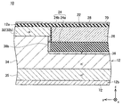
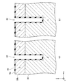
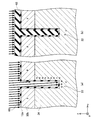
次に、図6に示すように、CVD法等によって、半導体基板12の上面12aとトレンチ22の内面に、犠牲酸化膜(酸化シリコン膜)60を形成する。次に、図7、8に示すように、レジスト樹脂等によってマスク62を形成する。なお、図7では、マスク62によって覆われる範囲をハッチングにより示している。また、図7のA−A線における断面が図8の断面(a)であり、図7のB−B線における断面が図8の断面(b)である。図7に示すように、マスク62には、トレンチ22を横断する開口部64が設けられている。図8の断面(b)に示すように、マスク62によって覆われる範囲では、上面12aがマスク62によって覆われるとともに、トレンチ22内にマスク62が充填される。すなわち、トレンチ22の側面と底面がマスク62によって覆われる。図8の断面(a)に示すように、マスク62によって覆われていない範囲では、上面12a、トレンチ22の内面(すなわち、側面と底面)において、犠牲酸化膜60が露出している。
Next, as shown in FIG. 6, a sacrificial oxide film (silicon oxide film) 60 is formed on the
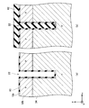
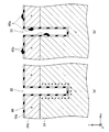
次に、図9に示すように、トレンチ22の深さ方向(すなわち、z方向)に対して傾斜した方向に沿ってp型不純物を照射する。これによって、マスク62に覆われていない範囲のトレンチ22の短手方向の側面とトレンチ22の底面に、p型不純物を注入する。なお、p型不純物は、犠牲酸化膜60を貫通して半導体基板に注入される。マスク62に覆われている範囲では、マスク62によって遮られることで、半導体基板12にp型不純物が注入されない。次に、図9とは反対向きに照射方向を傾斜させて、図9とは反対側のトレンチ22の側面(短手方向の側面)にもp型不純物を注入する。p型不純物の注入工程において、マスク62にもp型不純物が注入される。マスク62にp型不純物が注入されることで、マスク62の一部に変質層が形成される場合がある。
Next, as shown in FIG. 9, the p-type impurity is irradiated along the direction inclined with respect to the depth direction of the trench 22 (that is, the z direction). Thus, p-type impurities are implanted into the lateral side surface of the
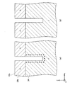
次に、マスク62をエッチングすることによって、マスク62を除去する。ここで、マスク62の一部に変質層が形成されていると、変質層を除去することができない。このため、図10に示すように、上面12a上の犠牲酸化膜60の表面とトレンチ22内の犠牲酸化膜60の表面に、変質層62aが残存する。
Next, the
次に、犠牲酸化膜60をエッチングすることによって、犠牲酸化膜60を除去する。犠牲酸化膜60を除去すると、犠牲酸化膜60の表面に付着している変質層62aも除去される。したがって、図11に示すように、上面12a及びトレンチ22の内面から、犠牲酸化膜60と変質層62aを好適に除去することができる。
Next, the
その後、半導体基板12を熱処理する。すると、トレンチ22の内面(より詳細には、短手方向の側面、長手方向の側面、及び、底面)に注入されたp型不純物が活性化する。これによって、第1接続領域38a、第2接続領域38b、及び、底部領域36が形成される。
Thereafter, the
その後、従来公知の方法によって、ゲート絶縁層24、ゲート電極26、層間絶縁膜28、ソース領域30、上部電極70、ドレイン領域35及び下部電極72が形成される。以上の処理によって、図1〜4に示すMOSFET10が完成する。
Thereafter, the
なお、上述した実施形態では、トレンチ22の短手方向の両側の側面に第1接続領域38aを形成した。しかしながら、トレンチ22の短手方向の片側の側面のみに第1接続領域38aが形成されてもよい。
In the embodiment described above, the
また、上述した実施形態では、トレンチ22の長手方向の側面へのp型不純物の注入工程を、トレンチ22の短手方向の側面へのp型不純物の注入工程とは別に実施した。しかしながら、図12に示すようにマスク62の開口部64をトレンチ22の長手方向の側面を含む範囲にも設け、トレンチ22の短手方向の側面へのp型不純物の注入と同時に、トレンチ22の長手方向の側面へのp型不純物の注入を実施してもよい。この場合、短手方向の側面と長手方向の側面の両方にp型不純物が注入されるように、p型不純物の照射方向を傾斜させる。
In the above-described embodiment, the step of injecting the p-type impurity into the side surface in the longitudinal direction of the
なお、上記実施形態のトレンチ22の短手方向の側面は、請求項1の第1側面の一例である。また、上記実施形態のトレンチ22の長手方向の側面は、請求項1の第2側面の一例である。
Note that the lateral side surface of the
以上、実施形態について詳細に説明したが、これらは例示にすぎず、特許請求の範囲を限定するものではない。特許請求の範囲に記載の技術には、以上に例示した具体例をさまざまに変形、変更したものが含まれる。
本明細書または図面に説明した技術要素は、単独あるいは各種の組み合わせによって技術有用性を発揮するものであり、出願時請求項記載の組み合わせに限定されるものではない。また、本明細書または図面に例示した技術は複数目的を同時に達成するものであり、そのうちの1つの目的を達成すること自体で技術有用性を持つものである。
The embodiments have been described in detail above, but these are merely examples and do not limit the scope of the claims. The technology described in the claims includes various modifications and changes of the specific examples illustrated above.
The technical elements described in this specification or the drawings exhibit technical usefulness alone or in various combinations, and are not limited to the combinations described in the claims at the time of filing. In addition, the technology exemplified in this specification or the drawings achieves a plurality of objects at the same time, and has technical usefulness by achieving one of them.
10 :MOSFET
12 :半導体基板
22 :トレンチ
24 :ゲート絶縁層
26 :ゲート電極
30 :ソース領域
32 :ボディ領域
34 :ドリフト領域
35 :ドレイン領域
36 :底部領域
38 :接続領域
10: MOSFET
12: Semiconductor substrate 22: Trench 24: Gate insulating layer 26: Gate electrode 30: Source region 32: Body region 34: Drift region 35: Drain region 36: Bottom region 38: Connection region
Claims (1)
前記スイッチング素子が、
半導体基板と、
前記半導体基板の上面に設けられたトレンチと、
前記トレンチの内面を覆っているゲート絶縁層と、
前記トレンチ内に配置されており、前記ゲート絶縁層によって前記半導体基板から絶縁されているゲート電極、
を有しており、
前記半導体基板が、
前記トレンチの短手方向の端部に位置する第1側面において前記ゲート絶縁層に接しているn型のソース領域と、
前記第1側面において前記ソース領域の下側で前記ゲート絶縁層に接しており、前記トレンチの長手方向の端部に位置する第2側面において前記ゲート絶縁層に接しているp型のボディ領域と、
前記第1側面に沿って前記ボディ領域から下側に伸びているp型の第1接続領域と、
前記第2側面に沿って前記ボディ領域から下側に伸びているp型の第2接続領域と、
前記ボディ領域の下側の前記第1側面の前記第1接続領域が存在しない範囲において前記ゲート絶縁層に接しており、前記ボディ領域によって前記ソース領域から分離されているn型のドリフト領域と、
前記トレンチの底面において前記ゲート絶縁層に接しており、前記第1接続領域と前記第2接続領域に接続されているp型の底部領域、
を有しており、
前記製造方法が、
前記トレンチを形成する工程と、
前記第1側面に犠牲酸化膜を形成する工程と、
前記犠牲酸化膜の表面に、前記第1側面の一部を覆うマスクを形成する工程と、
前記トレンチの深さ方向に対して傾斜した方向に沿った不純物照射によって、前記マスクに覆われていない範囲の前記第1側面にp型不純物を注入する工程と、
前記マスクをエッチングにより除去する工程と、
前記犠牲酸化膜をエッチングにより除去する工程、
を有する製造方法。 A method for manufacturing a switching element, comprising:
The switching element is
A semiconductor substrate;
A trench provided on an upper surface of the semiconductor substrate;
A gate insulating layer covering the inner surface of the trench;
A gate electrode disposed in the trench and insulated from the semiconductor substrate by the gate insulating layer;
Have
The semiconductor substrate is
An n-type source region in contact with the gate insulating layer on a first side surface located at an end of the trench in a short direction;
A p-type body region in contact with the gate insulating layer on the lower side of the source region on the first side surface and in contact with the gate insulating layer on a second side surface located at an end in the longitudinal direction of the trench; ,
A p-type first connection region extending downward from the body region along the first side surface;
A p-type second connection region extending downward from the body region along the second side surface;
An n-type drift region that is in contact with the gate insulating layer in a range where the first connection region on the first side surface under the body region does not exist, and is separated from the source region by the body region;
A p-type bottom region in contact with the gate insulating layer at a bottom surface of the trench and connected to the first connection region and the second connection region;
Have
The manufacturing method is
Forming the trench;
Forming a sacrificial oxide film on the first side surface;
Forming a mask covering a portion of the first side surface on the surface of the sacrificial oxide film;
Implanting p-type impurities into the first side surface in a range not covered by the mask by impurity irradiation along a direction inclined with respect to the depth direction of the trench;
Removing the mask by etching;
Removing the sacrificial oxide film by etching;
A manufacturing method comprising:
Priority Applications (1)
| Application Number | Priority Date | Filing Date | Title |
|---|---|---|---|
| JP2016078925A JP2017191817A (en) | 2016-04-11 | 2016-04-11 | Method for manufacturing switching element |
Applications Claiming Priority (1)
| Application Number | Priority Date | Filing Date | Title |
|---|---|---|---|
| JP2016078925A JP2017191817A (en) | 2016-04-11 | 2016-04-11 | Method for manufacturing switching element |
Publications (1)
| Publication Number | Publication Date |
|---|---|
| JP2017191817A true JP2017191817A (en) | 2017-10-19 |
Family
ID=60085376
Family Applications (1)
| Application Number | Title | Priority Date | Filing Date |
|---|---|---|---|
| JP2016078925A Pending JP2017191817A (en) | 2016-04-11 | 2016-04-11 | Method for manufacturing switching element |
Country Status (1)
| Country | Link |
|---|---|
| JP (1) | JP2017191817A (en) |
Cited By (6)
| Publication number | Priority date | Publication date | Assignee | Title |
|---|---|---|---|---|
| US10326015B2 (en) | 2017-02-17 | 2019-06-18 | Toyota Jidosha Kabushiki Kaisha | Switching element and method of manufacturing the same |
| JP2020096083A (en) * | 2018-12-12 | 2020-06-18 | トヨタ自動車株式会社 | Method for manufacturing trench gate type switching element |
| JP2020096082A (en) * | 2018-12-12 | 2020-06-18 | トヨタ自動車株式会社 | Semiconductor device |
| JP2022031964A (en) * | 2016-12-08 | 2022-02-22 | クリー インコーポレイテッド | Power semiconductor devices with gate trenches with ion implantation sidewalls and related methods |
| CN115050806A (en) * | 2021-03-09 | 2022-09-13 | 三菱电机株式会社 | Silicon carbide-metal oxide semiconductor field effect transistor |
| WO2025192194A1 (en) * | 2024-03-15 | 2025-09-18 | 富士電機株式会社 | Silicon carbide semiconductor device |
-
2016
- 2016-04-11 JP JP2016078925A patent/JP2017191817A/en active Pending
Cited By (13)
| Publication number | Priority date | Publication date | Assignee | Title |
|---|---|---|---|---|
| JP2022031964A (en) * | 2016-12-08 | 2022-02-22 | クリー インコーポレイテッド | Power semiconductor devices with gate trenches with ion implantation sidewalls and related methods |
| JP7309840B2 (en) | 2016-12-08 | 2023-07-18 | ウルフスピード インコーポレイテッド | Power semiconductor device with gate trench having ion implanted sidewalls and related method |
| US10326015B2 (en) | 2017-02-17 | 2019-06-18 | Toyota Jidosha Kabushiki Kaisha | Switching element and method of manufacturing the same |
| JP7230477B2 (en) | 2018-12-12 | 2023-03-01 | 株式会社デンソー | Manufacturing method of trench gate type switching element |
| JP2020096083A (en) * | 2018-12-12 | 2020-06-18 | トヨタ自動車株式会社 | Method for manufacturing trench gate type switching element |
| JP2020096082A (en) * | 2018-12-12 | 2020-06-18 | トヨタ自動車株式会社 | Semiconductor device |
| JP7135819B2 (en) | 2018-12-12 | 2022-09-13 | 株式会社デンソー | semiconductor equipment |
| JP2022137613A (en) * | 2021-03-09 | 2022-09-22 | 三菱電機株式会社 | SiC-MOSFET |
| CN115050806A (en) * | 2021-03-09 | 2022-09-13 | 三菱电机株式会社 | Silicon carbide-metal oxide semiconductor field effect transistor |
| US12107158B2 (en) | 2021-03-09 | 2024-10-01 | Mitsubishi Electric Corporation | SiC-mosfet |
| JP7565828B2 (en) | 2021-03-09 | 2024-10-11 | 三菱電機株式会社 | SiC-MOSFET |
| CN115050806B (en) * | 2021-03-09 | 2025-11-04 | 三菱电机株式会社 | Silicon carbide-metal oxide semiconductor field-effect transistor |
| WO2025192194A1 (en) * | 2024-03-15 | 2025-09-18 | 富士電機株式会社 | Silicon carbide semiconductor device |
Similar Documents
| Publication | Publication Date | Title |
|---|---|---|
| JP6266166B2 (en) | Silicon carbide semiconductor device and manufacturing method thereof | |
| CN105280711B (en) | Charge compensation structure and fabrication therefor | |
| JP6606007B2 (en) | Switching element | |
| US10468520B2 (en) | Switching element and method of manufacturing the same | |
| JP2019087611A (en) | Switching element and manufacturing method thereof | |
| JP6571467B2 (en) | Insulated gate type switching element and manufacturing method thereof | |
| JP6563639B2 (en) | Semiconductor device and manufacturing method of semiconductor device | |
| JP6493372B2 (en) | Semiconductor device | |
| JP2018056304A (en) | Switching device and manufacturing method | |
| JP2017191817A (en) | Method for manufacturing switching element | |
| CN106537602A (en) | Switching element | |
| WO2016046900A1 (en) | Silicon carbide semiconductor device, method for manufacturing silicon carbide semiconductor device, and method for designing silicon carbide semiconductor device | |
| CN113169229A (en) | Silicon carbide semiconductor device and method for manufacturing same | |
| CN102468298A (en) | Accumulator Field Effect Transistor with Integrated Clamp Circuit | |
| CN109075197B (en) | Semiconductor switching element | |
| US10374081B2 (en) | Semiconductor switching element | |
| JP6299658B2 (en) | Insulated gate type switching element | |
| JP2017174961A (en) | Method for manufacturing switching element | |
| CN108305893B (en) | semiconductor device | |
| JP2020064910A (en) | Switching element | |
| CN111162116A (en) | Semiconductor device and method of manufacturing the same | |
| JP7560344B2 (en) | Semiconductor Device | |
| JP2024137200A (en) | Field-effect transistor | |
| JP2018085383A (en) | Switching element | |
| JP2018046254A (en) | Switching element |