WO2017150231A1 - 樹脂シート - Google Patents
樹脂シート Download PDFInfo
- Publication number
- WO2017150231A1 WO2017150231A1 PCT/JP2017/006047 JP2017006047W WO2017150231A1 WO 2017150231 A1 WO2017150231 A1 WO 2017150231A1 JP 2017006047 W JP2017006047 W JP 2017006047W WO 2017150231 A1 WO2017150231 A1 WO 2017150231A1
- Authority
- WO
- WIPO (PCT)
- Prior art keywords
- resin
- substrate
- resin sheet
- solder resist
- resin layer
- Prior art date
- Legal status (The legal status is an assumption and is not a legal conclusion. Google has not performed a legal analysis and makes no representation as to the accuracy of the status listed.)
- Ceased
Links
Images
Classifications
-
- C—CHEMISTRY; METALLURGY
- C08—ORGANIC MACROMOLECULAR COMPOUNDS; THEIR PREPARATION OR CHEMICAL WORKING-UP; COMPOSITIONS BASED THEREON
- C08J—WORKING-UP; GENERAL PROCESSES OF COMPOUNDING; AFTER-TREATMENT NOT COVERED BY SUBCLASSES C08B, C08C, C08F, C08G or C08H
- C08J5/00—Manufacture of articles or shaped materials containing macromolecular substances
- C08J5/18—Manufacture of films or sheets
-
- C—CHEMISTRY; METALLURGY
- C08—ORGANIC MACROMOLECULAR COMPOUNDS; THEIR PREPARATION OR CHEMICAL WORKING-UP; COMPOSITIONS BASED THEREON
- C08K—Use of inorganic or non-macromolecular organic substances as compounding ingredients
- C08K3/00—Use of inorganic substances as compounding ingredients
- C08K3/34—Silicon-containing compounds
- C08K3/36—Silica
-
- C—CHEMISTRY; METALLURGY
- C08—ORGANIC MACROMOLECULAR COMPOUNDS; THEIR PREPARATION OR CHEMICAL WORKING-UP; COMPOSITIONS BASED THEREON
- C08L—COMPOSITIONS OF MACROMOLECULAR COMPOUNDS
- C08L101/00—Compositions of unspecified macromolecular compounds
-
- C—CHEMISTRY; METALLURGY
- C08—ORGANIC MACROMOLECULAR COMPOUNDS; THEIR PREPARATION OR CHEMICAL WORKING-UP; COMPOSITIONS BASED THEREON
- C08L—COMPOSITIONS OF MACROMOLECULAR COMPOUNDS
- C08L63/00—Compositions of epoxy resins; Compositions of derivatives of epoxy resins
-
- C—CHEMISTRY; METALLURGY
- C08—ORGANIC MACROMOLECULAR COMPOUNDS; THEIR PREPARATION OR CHEMICAL WORKING-UP; COMPOSITIONS BASED THEREON
- C08L—COMPOSITIONS OF MACROMOLECULAR COMPOUNDS
- C08L79/00—Compositions of macromolecular compounds obtained by reactions forming in the main chain of the macromolecule a linkage containing nitrogen with or without oxygen or carbon only, not provided for in groups C08L61/00 - C08L77/00
-
- H—ELECTRICITY
- H05—ELECTRIC TECHNIQUES NOT OTHERWISE PROVIDED FOR
- H05K—PRINTED CIRCUITS; CASINGS OR CONSTRUCTIONAL DETAILS OF ELECTRIC APPARATUS; MANUFACTURE OF ASSEMBLAGES OF ELECTRICAL COMPONENTS
- H05K3/00—Apparatus or processes for manufacturing printed circuits
- H05K3/22—Secondary treatment of printed circuits
- H05K3/28—Applying non-metallic protective coatings
-
- H—ELECTRICITY
- H05—ELECTRIC TECHNIQUES NOT OTHERWISE PROVIDED FOR
- H05K—PRINTED CIRCUITS; CASINGS OR CONSTRUCTIONAL DETAILS OF ELECTRIC APPARATUS; MANUFACTURE OF ASSEMBLAGES OF ELECTRICAL COMPONENTS
- H05K3/00—Apparatus or processes for manufacturing printed circuits
- H05K3/22—Secondary treatment of printed circuits
- H05K3/28—Applying non-metallic protective coatings
- H05K3/281—Applying non-metallic protective coatings by means of a preformed insulating foil
Definitions
- the present invention relates to a resin sheet.
- Patent Document 1 discloses a technique related to a solder resist for a printed wiring board.
- a thermosetting resin composition used for a solder resist is used in the form of a dry film coated and dried. Specifically, the above dry film is obtained by coating on a carrier film and evaporating and drying an organic solvent contained in the thermosetting resin composition. And it describes that a dry film is affixed on base materials, such as a printed wiring board and a flexible printed wiring board, a carrier film is peeled off, and a dry film is hardened.
- the present inventor has balanced the characteristics of the semi-cured product (resin film in the B stage state) and the cured product (cured resin film) from the viewpoint of improving the yield of the circuit board.
- the following findings were obtained.
- (1) circuit boards such as printed wiring boards are becoming thinner. Along with the thinning, the deflection generated in the circuit board has become apparent. It has been found that when the deflection occurs in the circuit board, the transport reliability such as the difficulty of transporting the board is lowered during the mounting process. Even if a method of stiffening the substrate itself was adopted, the deflection was not sufficiently suppressed.
- the substrate deflection is improved by increasing the rigidity of the solder resist (cured resin film) formed on the surface of the substrate. Has been found to be sufficiently suppressed. Although the detailed mechanism is not clear, by increasing the rigidity of the solder resist formed on the substrate surface, the substrate can be pulled up like a suspension bridge structure. It is thought that a rigid structure can be created and the deflection of the substrate can be suppressed.
- the resin layer was applied to the wiring formed on the substrate surface by using the minimum value of the complex dynamic viscosity in the measurement range of 50 to 200 ° C. as an index. It has been found that when the resin is embedded, the resin layer can be stably evaluated for the resin flowing out of the substrate.
- the present inventor has made extensive studies based on the above knowledge, and regarding the resin film used for the solder resist, the storage elastic modulus at 30 ° C.
- the present invention has been completed.
- a carrier substrate A resin sheet used for a solder resist, comprising a resin layer disposed on the carrier substrate and comprising a resin composition for a solder resist,
- the resin layer has a thickness of 1 ⁇ m or more and 50 ⁇ m or less, When the minimum value of the complex dynamic viscosity in a measurement range of 50 to 200 ° C., a temperature increase rate of 3 ° C./min, and a frequency of 62.83 rad / sec is ⁇ by the dynamic viscoelasticity test in the B stage state of the resin layer.
- ⁇ is 100 Pa ⁇ s or more and 3000 Pa ⁇ s or less
- a resin sheet is provided in which the cured product of the resin layer has a storage elastic modulus at 30 ° C. of 7 GPa or more and 40 GPa or less.
- a resin sheet used for a solder resist with excellent transport reliability is provided.
- the resin sheet of the present embodiment includes a carrier base material and a resin layer that is disposed on the carrier base material and includes a resin composition for solder resist.
- the resin sheet is used for a solder resist.
- the resin sheet of this embodiment satisfies the following conditions. -The film thickness of the resin layer is 1 ⁇ m or more and 50 ⁇ m or less.
- the minimum value of the complex dynamic viscosity is ⁇ in a measurement range of 50 to 200 ° C., a temperature increase rate of 3 ° C./min, and a frequency of 62.83 rad / sec, according to a dynamic viscoelasticity test in the B stage state of the resin layer ⁇ is 100 Pa ⁇ s or more and 3000 Pa ⁇ s or less.
- cured material of a resin layer is 7 GPa or more and 40 GPa or less.
- the resin layer of the present embodiment is a thin layer as defined by the film thickness and a high rigidity as defined by the storage elastic modulus at 30 ° C. of the cured product.
- Such a resin layer can be optimally used as a solder resist for a thin substrate or a coreless structure substrate.
- the inventor examined when the inventor examined, when the total film thickness of the circuit board (total film thickness of the substrate and the solder resist) is a thin layer of, for example, 100 ⁇ m or less, the strength of the thin substrate alone is sufficient. It turned out to be gone. Specifically, since wiring such as copper wiring formed on the surface of the substrate becomes a weight, even if the rigidity of the single substrate is increased, the deflection of the substrate cannot be sufficiently suppressed.
- solder resist having high rigidity (cured product of the resin layer of the present embodiment) on the surface of the substrate, the above-described deflection of the substrate can be suppressed.
- a high-rigidity solder resist is formed to cover the wiring, the board that was bent by the weight of the wiring can be pulled up like a suspension bridge structure, It is thought that it is possible to create a rigid structure that exceeds the rigidity.
- the resin layer in the B stage state has fluidity defined by the minimum value of the complex dynamic viscosity by the dynamic viscoelasticity test.
- the minimum value of the complex dynamic viscosity is set to the above lower limit value or more, it is possible to suppress the resin flow of the resin layer after the B-stage resin layer is formed on the surface of the substrate. Become.
- the transportability is excellent by appropriately controlling the fluidity in the semi-cured product (resin layer in the B stage state) while increasing the rigidity of the cured product.
- a resin layer can be obtained. That is, by using the resin sheet of the present embodiment, the manufacturing stability from the process of forming the solder resist on the circuit board to the process of mounting the electronic components on the circuit board can be improved, so the manufacturing process of the electronic device Overall yield can be increased.
- the solder resist resin composition of the present embodiment is a varnish-like resin composition.
- the resin layer of this embodiment can be obtained by making the said resin composition for solder resists into a film form. By curing the resin layer, a solder resist is obtained.
- thermosetting resin composition containing a thermosetting resin can be used for the resin composition for a solder resist of the present embodiment.
- the thermosetting resin is not particularly limited.
- the thermosetting resin may be a liquid resin that is liquid at room temperature (25 ° C.). These can be used alone or in combination of two or more.
- the thermosetting resin preferably includes an epoxy resin.
- the epoxy resin (A) includes, for example, bisphenol A type epoxy resin, bisphenol F type epoxy resin, bisphenol E type epoxy resin, bisphenol S type epoxy resin, bisphenol M type epoxy resin (4,4 ′-(1 , 3-phenylenediisopridiene) bisphenol type epoxy resin), bisphenol P type epoxy resin (4,4 ′-(1,4-phenylenediisopridiene) bisphenol type epoxy resin), bisphenol Z type epoxy resin (4 , 4'-cyclohexyldiene bisphenol type epoxy resin); phenol novolac type epoxy resin, cresol novolac type epoxy resin, tetraphenol group ethane type novolak type epoxy resin, condensed ring aromatic hydrocarbon structure Novolak type epoxy resins such as novolak type epoxy resins, biphenyl type epoxy resins, xylylene type epoxy resins, aralkyl type epoxy resins such as biphenyl aralkyl type epoxy resins, naphth
- an epoxy resin having a naphthalene skeleton from the viewpoint of improving the embedding property of the solder resist and the surface smoothness. Thereby, low linear expansion and high elastic modulus of the solder resist can be achieved. It is also possible to improve the workability by improving the rigidity of the circuit board, and to improve the reflow resistance and suppress the warpage in the semiconductor package. In addition, from the viewpoint of improving the embedding property of the solder resist, it is particularly preferable to include an epoxy resin having a trifunctional or higher functional naphthalene skeleton.
- n is an integer of 0 to 10
- R 1 and R 2 are each independently a hydrogen atom, an alkyl group having 1 to 6 carbon atoms, or an alkoxy group having 1 to 6 carbon atoms.
- the content of the epoxy resin (A) is, for example, preferably 3% by weight or more, and more preferably 5% by weight or more with respect to the entire solder resist resin composition.
- content of an epoxy resin (A) is, for example, preferably 40% by weight or less, and more preferably 35% by weight or less, based on the entire solder resist resin composition.
- content of an epoxy resin (A) below the said upper limit, the heat resistance and moisture resistance of a solder resist formed using the resin composition for solder resists can be aimed at.
- the whole resin composition for solder resist refers to the whole component except the solvent contained in the resin composition for solder resist. The same applies hereinafter.
- the resin composition for solder resists of this embodiment may further contain a filler. That is, the resin composition for solder resist can contain a thermosetting resin and a filler. An inorganic filler can be used as the filler according to the present embodiment.
- the inorganic filler examples include, but are not limited to, silicates such as talc, calcined clay, unfired clay, mica, and glass; oxides such as titanium oxide, alumina, boehmite, silica, and fused silica; calcium carbonate Carbonates such as magnesium carbonate and hydrotalcite; hydroxides such as aluminum hydroxide, magnesium hydroxide and calcium hydroxide; sulfates or sulfites such as barium sulfate, calcium sulfate and calcium sulfite; zinc borate and metaborates Borates such as barium oxide, aluminum borate, calcium borate and sodium borate; nitrides such as aluminum nitride, boron nitride, silicon nitride and carbon nitride; titanates such as strontium titanate and barium titanate Can be mentioned.
- silicates such as talc, calcined clay, unfired clay, mica, and glass
- oxides such as titanium oxide
- the silica according to this embodiment is not particularly limited, but may include, for example, at least one of spherical silica and crushed silica. From the viewpoint of improving the embedding property and surface smoothness of the solder resist, it is more preferable to include spherical silica.
- the silica may be, for example, fused spherical silica.
- the lower limit of the average particle diameter D 50 of the filler is not particularly limited, is preferably at least 0.01 [mu] m, more preferably not less than 0.05 .mu.m.
- the upper limit of the average particle diameter D 50 of the filler is not particularly limited, is preferably from 5.0 .mu.m, more preferably 2.0 ⁇ m or less, more preferably 1.0 ⁇ m or less. Thereby, the balance between fluidity and mechanical strength can be improved.
- an average particle diameter D 50 may be used fine particles of silica is 2nm or 100nm or less.
- the embedding property and surface smoothness of a solder resist can be improved more effectively.
- the particulate silica having an average particle diameter D 50 is 2nm or 100nm or less, that the average particle diameter D 50 comprises a 100nm excess of silica, together in the resin composition for a solder mask, filling properties And an example of a preferred embodiment for improving surface smoothness.
- the average particle diameter D 50 of the filler is for example a laser diffraction particle size distribution analyzer (HORIBA Ltd., LA-500) can be measured using a.
- the filler may include one kind or two or more kinds.
- a silica raw material having a silica concentration of 10 wt% or more and 90 wt% or less As the silica. From the viewpoint of improving the mechanical strength of the circuit board, it is particularly preferable to use a silica raw material having a silica concentration of 50% by weight or more and 90% by weight or less, for example. Further, from the viewpoint of suppressing the deflection of the circuit board and improving the moisture absorption reliability of the electronic device, for example, a silica raw material having a silica concentration of 50% by weight to 90% by weight and a silica concentration of 10% by weight to 50% by weight. It is particularly preferable to use a silica raw material of less than%.
- the content of the filler is preferably 30% by weight or more, and more preferably 50% by weight or more with respect to the entire resin composition for a solder resist, for example.
- the content of a filler is preferably 30% by weight or more, and more preferably 50% by weight or more with respect to the entire resin composition for a solder resist, for example.
- the solder resist can be made to have a low linear expansion and a high elastic modulus, thereby contributing to the reduction of the deflection of the circuit board and the warp of the semiconductor package obtained from the circuit board.
- the content of the filler is preferably 90% by weight or less, and more preferably 85% by weight or less, for example, with respect to the entire resin composition for a solder resist.
- the resin composition for solder resists of this embodiment can further contain cyanate resin (C).
- C Cyclone resin
- the solder resist can be reduced in linear expansion and improved in elastic modulus and rigidity. Further, it is possible to contribute to improvement of heat resistance and moisture resistance of the obtained electronic device.
- the cyanate resin (C) is a resin having a cyanate group (—O—CN) in the molecule, and a resin having two or more cyanate groups in the molecule can be used.
- a resin having two or more cyanate groups in the molecule can be used.
- said cyanate resin (C) For example, dicyclopentadiene type cyanate ester resin, phenol novolak type cyanate ester resin, novolak type cyanate resin, bisphenol A type cyanate resin, bisphenol E type cyanate resin, tetramethyl Examples thereof include bisphenol type cyanate resins such as bisphenol F type cyanate resins, and naphthol aralkyl type cyanate resins.
- the said cyanate resin (C) is not specifically limited, For example, it can obtain by making a halogenated cyanide compound, phenols, or naphthol react.
- cyanate resins include cyanate resins obtained by reaction of phenol novolac type polyhydric phenols with cyanogen halide, and cyanates obtained by reaction of cresol novolac type polyhydric phenols with cyanogen halide.
- a cyanate resin obtained by a reaction of a naphthol aralkyl type polyvalent naphthol with a cyanogen halide You may use the said cyanate resin 1 type or in combination of 2 or more types.
- a phenol novolac-type cyanate ester resin dicyclopentadiene-type cyanate ester resin, or naphthol aralkyl-type cyanate resin. It is particularly preferable to include a phenol novolac type cyanate ester resin.
- the content of the cyanate resin (C) is, for example, preferably 3% by weight or more and more preferably 5% by weight or more with respect to the entire resin composition for solder resist.
- the content of the cyanate resin (C) is, for example, preferably 40% by weight or less, and more preferably 35% by weight or less, based on the entire solder resist resin composition.
- the resin composition for solder resists of this embodiment can further contain, for example, a curing accelerator (D).
- a curing accelerator (D) The resin composition for solder resists of this embodiment can further contain, for example, a curing accelerator (D).
- the curing accelerator (D) one that accelerates the curing reaction of the epoxy resin (A) can be used, and the type thereof is not particularly limited.
- hardening accelerator (D) of this embodiment For example, zinc naphthenate, cobalt naphthenate, tin octylate, cobalt octylate, zinc octylate, bisacetylacetonate cobalt (II), tris Organometallic salts such as acetylacetonate cobalt (III), tertiary amines such as triethylamine, tributylamine, diazabicyclo [2.2.2] octane, tetraphenylphosphonium tetraphenylborate (TPP-K), tetraphenylphosphonium ⁇ Quaternary phosphonium compounds such as tetrakis (4-methylphenyl) borate (TPP-MK), bis
- the onium salt compound used as the curing accelerator (D) is not particularly limited, for example, a compound represented by the following general formula (2) can be used.
- R 3 , R 4 , R 5 and R 6 are each an organic group having a substituted or unsubstituted aromatic ring or heterocyclic ring, or a substituted or unsubstituted aliphatic group. represents a group, optionally being the same or different .
- a - is an anion of n (n ⁇ 1) number of proton donor having a proton capable of releasing the extracellular molecules in at least one or more intramolecular or, Indicates the complex anion)
- the content of the curing accelerator (D) is, for example, preferably 0.1% by weight or more, and more preferably 0.3% by weight or more with respect to the entire solder resist resin composition.
- content of a hardening accelerator (D) is, for example, preferably 10% by weight or less, and more preferably 5% by weight or less, based on the entire solder resist resin composition.
- the resin composition for solder resists of this embodiment can further contain a colorant (E), for example.
- the colorant (E) of the present embodiment includes one or more selected from dyes, pigments, and pigments such as green, red, blue, yellow, and black. Among these, from the viewpoint of improving the visibility of the opening and the like, a green colorant can be included, but a green dye may be included.
- the green colorant may include one or more known colorants such as anthraquinone, phthalocyanine, and perylene.
- black dye examples include azo-based metal complex black dyes and organic black dyes such as anthraquinone compounds. Although it does not specifically limit as said black dye, For example, Kayase Black AN (made by Nippon Kayaku Co., Ltd.), Kayase Black G (made by Nippon Kayaku Co., Ltd.), etc. are mentioned. In this embodiment, you may use 1 type, or 2 or more types of black pigments.
- the lower limit of the content of the black dye is preferably 0.01% by weight or more, more preferably 0.05% by weight or more, based on the entire solder resist resin composition. It is particularly preferable that the content be 07% by weight or more.
- the marking performance of a laser such as a solder resist YAG laser can be improved.
- the upper limit of the content of the black dye is preferably 1.0% by weight or less, more preferably 0.9% by weight or less, based on the entire solder resist resin composition. More preferably, it is 8 wt% or less. This makes it possible to realize a solder resist colored other than black.
- the total content of the colorant (E) is, for example, preferably 0.05% by weight or more, more preferably 0.1% by weight or more, with respect to the entire solder resist resin composition. .
- content of a coloring agent (E) is, for example, preferably 5% by weight or less, more preferably 3% by weight or less, with respect to the entire solder resist resin composition.
- the solder resist resin composition of the present embodiment includes a coupling agent, a leveling agent, a curing agent, a photosensitizer, an antifoaming agent, an ultraviolet absorber, a foaming agent, and an antioxidant as necessary.
- a coupling agent e.g., a coupling agent, a leveling agent, a curing agent, a photosensitizer, an antifoaming agent, an ultraviolet absorber, a foaming agent, and an antioxidant as necessary.
- One or two or more additives selected from flame retardants and ion scavengers may be added.
- the coupling agent examples include silane coupling agents such as epoxy silane coupling agents, cationic silane coupling agents, and amino silane coupling agents, titanate coupling agents, and silicone oil type coupling agents.
- the content of the coupling agent is not particularly limited. For example, it may be 0.05% by weight or more and 5% by weight or less, and further 0.2% by weight or more and 3% by weight with respect to the entire resin composition for solder resist. It is good also as weight% or less.
- the leveling agent include acrylic copolymers.
- curing agent examples include phenol resins such as phenol novolak resin, cresol novolak resin, arylalkylene type novolak resin, and the like.
- curing agent is not specifically limited, For example, it is good also as 0.05 to 10 weight% with respect to the whole resin composition for soldering resists, Furthermore, 0.2 to 5 weight% % Or less.
- the photosensitive agent include photosensitive diazoquinone compounds.
- the resin composition for solder resists according to the present embodiment may not include a fiber substrate such as a glass fiber substrate or a paper substrate. Thereby, it is possible to realize a solder resist resin composition particularly suitable for forming a solder resist.
- the resin sheet according to the present embodiment can include a carrier substrate and a resin layer formed on the carrier substrate.
- the resin layer of this embodiment is in a B-stage state and is composed of a dry film of the above-described resin composition for solder resist.
- the resin sheet in the present embodiment may have a sheet shape (a sheet shape) or a roll shape that can be wound.
- the method for forming the solder resist resin composition on the carrier substrate is not particularly limited.
- the resin composition for the solder resist is dissolved and dispersed in a solvent to prepare a resin varnish, After coating the resin varnish on the carrier substrate using various coater devices, drying this, spraying the resin varnish on the carrier substrate using a spray device, and then drying this, etc.
- the method of drying the resin varnish after applying the resin varnish to the carrier substrate using various coaters such as a comma coater and a die coater is preferable. Thereby, the resin sheet which does not have a void and has the thickness of the uniform resin layer can be manufactured efficiently.
- the resin varnish of the present embodiment is a solder resist resin composition containing a solvent.
- the solid content of the solder resist resin composition is, for example, preferably 30% by weight to 80% by weight, and more preferably 40% by weight to 70% by weight.
- operativity and film forming property is obtained.
- the resin composition for a varnish-like solder resist includes, for example, the above-described components, an ultrasonic dispersion method, a high-pressure collision dispersion method, a high-speed rotation dispersion method, a bead mill method, a high-speed shear dispersion method, and a rotation and revolution dispersion method. It can prepare by melt
- solvent examples include acetone, methyl ethyl ketone, methyl isobutyl ketone, toluene, ethyl acetate, cyclohexane, heptane, cyclohexane, cyclohexanone, tetrahydrofuran, dimethylformamide, dimethylacetamide, dimethyl sulfoxide, ethylene glycol, cellosolve, and carbitol. , Anisole, and one or more selected from organic solvents such as N-methylpyrrolidone.
- a resin sheet having a B-stage (semi-cured) resin layer formed on a carrier substrate can be obtained.
- the semi-cured state (B-stage state) of the resin layer is calculated from DSC measurement results obtained by measuring an uncured resin layer and a cured resin layer with a DSC (differential scanning calorimeter).
- the reaction rate is more than 0% and 60% or less, preferably 0.5% or more and 55% or less, and more preferably 1% or more and 50% or less. Thereby, the handleability of the resin layer can be improved.
- the solvent content of the resin layer in the B-stage state can be defined as 5% by weight or less with respect to the entire resin composition for solder resist.
- the solvent removal treatment can be performed on the solder resist resin composition under conditions of, for example, 100 ° C. to 150 ° C. for 1 minute to 5 minutes. This makes it possible to sufficiently remove the solvent while suppressing the curing of the thermosetting resin film.
- the cured state (C stage state) of the cured product of the resin layer of the present embodiment is that the reaction rate calculated from the DSC measurement result is greater than 75%, more preferably 85% or more as described above. More preferably, it means that the state is 95% or more. Thereby, the rigidity of the cured product of the resin layer can be improved.
- the resin layer can be cured by heat treatment.
- a lower limit of the curing temperature of this embodiment For example, 190 degreeC or more is preferable, 200 degreeC or more is more preferable, and 210 degreeC or more is further more preferable.
- it does not specifically limit as an upper limit of the said curing temperature For example, it can be set to 260 degrees C or less, 240 degrees C or less, and 220 degrees C or less may be sufficient.
- a polymer film or a metal foil can be used as the carrier substrate.
- the polymer film is not particularly limited.
- polyolefin such as polyethylene and polypropylene
- polyester such as polyethylene terephthalate and polybutylene terephthalate
- release paper such as polycarbonate and silicone sheet
- heat resistance such as fluorine resin and polyimide resin.
- thermoplastic resin sheet having properties.
- metal foil For example, copper and / or a copper-type alloy, aluminum and / or an aluminum-type alloy, iron and / or an iron-type alloy, silver and / or a silver-type alloy, gold
- money and gold-type Examples include alloys, zinc and zinc alloys, nickel and nickel alloys, tin and tin alloys. Among these, a sheet made of polyethylene terephthalate is most preferable because it is inexpensive and easy to adjust the peel strength. Thereby, it becomes easy to peel from the said resin sheet with moderate intensity
- the thickness of the carrier substrate is not particularly limited, but may be, for example, 10 ⁇ m or more and 100 ⁇ m or less, or 10 ⁇ m or more and 70 ⁇ m or less. Thereby, the handleability at the time of manufacturing a resin sheet is favorable and preferable.
- the resin layer of the present embodiment may be a single layer or multiple layers, and may include one or more of the above films.
- the said resin sheet When the said resin sheet is a multilayer, it may be comprised by the same kind and may be comprised by different types.
- the method of forming two or more resin layers is not particularly limited.
- the first resin layer and the second resin obtained by applying a solder resist resin composition to a carrier substrate.
- the two resin layers are obtained by pasting the layers together and then drying them.
- the 1st resin layer is obtained by apply
- coating and drying the resin composition for solder resists on the 1st resin layer is mentioned.
- coating and drying two layers on a carrier base material simultaneously can also be used.
- the lower limit of the film thickness of the resin layer of the present embodiment is not particularly limited, but is, for example, 1 ⁇ m or more, preferably 5 ⁇ m or more, and more preferably 10 ⁇ m or more. Thereby, it can be set as the resin layer excellent in manufacturing stability and mechanical strength.
- the upper limit of the film thickness of a resin layer is 50 micrometers or less, for example, Preferably it is 40 micrometers or less, More preferably, it is 30 micrometers or less. Thereby, the entire thickness of the circuit board can be reduced.
- the minimum value of the complex dynamic viscosity in the measurement range of 50 to 200 ° C., the temperature increase rate of 3 ° C./min, and the frequency of 62.83 rad / sec by the dynamic viscoelasticity test in the B stage state of the resin layer of this embodiment is ⁇
- the lower limit value of ⁇ is, for example, 100 Pa ⁇ s or more, preferably 150 Pa ⁇ s or more, and more preferably 200 Pa ⁇ s or more.
- the upper limit of ⁇ is not particularly limited, but is, for example, 3000 Pa ⁇ s or less, preferably 2500 Pa ⁇ s or less, and more preferably 2000 Pa ⁇ s or less.
- the embedding property of the resin layer can be improved. That is, embedding in the wiring formed on the substrate surface is facilitated, and adhesion between the substrate and the resin layer can be stably obtained. In addition, the handling can be improved.
- the complex dynamic viscosity can be measured as follows.
- the resin layer of the resin sheet is cut out to obtain a measurement sample, and the complex dynamic viscosity ⁇ is measured under the following conditions using a dynamic viscoelasticity measuring device (manufactured by Anton Paar, device name Physica MCR-301). .
- Frequency 62.83 rad / sec Measurement temperature: 50 to 200 ° C., heating rate 3 ° C./min
- Geometry Parallel plate Plate diameter: 10mm Load (normal force): 0N (constant) Strain: 0.3% Measurement atmosphere: Air
- the lower limit value of the resin flow amount in the B stage state of the resin layer of the present embodiment is not particularly limited, but is, for example, 5% by weight or more, 8% by weight or more, or 10% by weight or more. Thereby, the yield in manufacture of a circuit board can be raised.
- the upper limit of the said resin flow amount is less than 70 weight%, for example, Preferably it is 65 weight% or less, More preferably, it is 60 weight% or less, More preferably, it is 50 weight% or less. Thereby, in the bonding process of a board
- the resin flow amount can be measured under the following measurement conditions. ⁇ Punching the whole substrate with a sample size of 113mm ⁇ ⁇ 4 layers with the substrate (W0) ⁇ Heating and pressurizing under conditions of temperature 171 ⁇ 3 °C and pressure 750 ⁇ 50kPa ⁇ Measurement of weight excluding resin protruding from 113mm ⁇ (W1) (W0-W1) / (W0-base material weight) ⁇ 100
- the lower limit of the storage elastic modulus at 30 ° C. of the cured product of the resin layer obtained by heat treatment at 200 ° C. for 1 hour is, for example, 7 GPa or more, preferably 10 GPa or more, more preferably Is 13 GPa or more, more preferably 14 GPa or more.
- the substrate Furthermore, it is possible to prevent the substrate from being chipped or caught during transportation due to the deflection of the substrate. Further, it is possible to suppress warpage of a semiconductor package (electronic device) including this circuit board.
- the upper limit of the storage elastic modulus at 30 ° C. of the cured product is not particularly limited, for example, it may be 40 GPa or less, 30 GPa or less, or 20 GPa or less. Thereby, the balance of conveyance reliability and handling property can be aimed at.
- the lower limit of the storage elastic modulus at 260 ° C. of the cured product of the resin layer obtained by heat treatment at 200 ° C. for 1 hour is, for example, 0.2 GPa or more, preferably 0.5 GPa or more. Yes, more preferably 1.5 GPa or more, still more preferably 2.0 GPa or more.
- cured material is not specifically limited, For example, it may be 10 GPa or less, may be 8 GPa or less, and may be 6 GPa or less. A balance between transport reliability and handling can be achieved.
- the upper limit value of the storage elastic modulus ratio in the present embodiment may be, for example, 5.0 or less, more preferably 0.90 or less, particularly preferably 0.8 or less, and most preferably 0.7 or less. Thereby, also in the use environment where a thermal history is repeatedly added, the bending of the circuit board provided with the solder resist which consists of the hardened
- the lower limit value of the storage elastic modulus ratio is not particularly limited, but may be, for example, 0.1 or more, 0.3 or more, or 0.4 or more. Thereby, the balance of conveyance reliability and handling property can be aimed at.
- the lower limit value of the glass transition temperature of the cured product of the resin layer obtained by heat treatment at 200 ° C. for 1 hour is, for example, 160 ° C. or higher, more preferably 180 ° C. or higher, and further preferably. Is 190 ° C. or higher. Thereby, it becomes possible to improve the heat resistance and reflow resistance of the resin layer.
- the upper limit of the glass transition temperature of the cured product of the resin layer is not particularly limited, but may be, for example, 350 ° C. or lower.
- the storage elastic modulus and the glass transition temperature are obtained, for example, by performing a dynamic viscoelasticity test using a dynamic viscoelasticity measuring device under conditions of a frequency of 1 Hz and a heating rate of 5 ° C./min. It can be calculated from the measurement result.
- a dynamic viscoelasticity measuring apparatus For example, the Seiko Instruments make and DMS6100 can be used.
- the lower limit value of the linear expansion coefficient of the cured product of the resin layer obtained by heat treatment at 200 ° C. for 1 hour is not particularly limited, but may be, for example, 1 ppm / ° C. or more. It may be 5 ppm / ° C. or higher, or 10 ppm / ° C. or higher. Thereby, the circuit board which can manufacture the semiconductor package excellent in durability can be implement
- the upper limit value of the linear expansion coefficient of the cured product of the resin layer below the glass transition temperature is, for example, 35 ppm / ° C. or less, preferably 30 ppm / ° C. or less, more preferably 25 ppm / ° C. or less. Thereby, it becomes possible to suppress warpage of a semiconductor package including the solder resist made of the resin layer.
- an average at 25 to 50 ° C. of the linear expansion coefficient obtained by measuring at a temperature rising rate of 10 ° C./min using TMA (thermal analyzer) is calculated, and this is calculated.
- the linear expansion coefficient at a temperature lower than the glass transition temperature can be obtained.
- the amount of deflection measured under the following conditions is, for example, less than 35 mm, preferably 20 mm or less, and more preferably 15 mm or less.
- the amount of deflection is an index for evaluating the rigidity of the solder resist found by the present inventors. That is, as a result of performing various experiments, it was found that by using the deflection amount as an index of deflection and setting the deflection amount to a predetermined value or less, it is possible to obtain a resin sheet with excellent transport reliability and a circuit board using the resin sheet. .
- the measurement conditions of the deflection amount in the present embodiment are, for example, as follows. First, after applying the solder resist resin composition to the carrier substrate, the solvent is removed under conditions of 140 ° C. for 2 minutes to form a resin layer having a predetermined thickness.
- a double-sided copper-clad laminate is prepared by laminating a copper foil having a thickness of 12 ⁇ m on one side and the other side of a core substrate (50 mm ⁇ 85 mm, predetermined thickness). Next, the copper foil of the double-sided copper-clad laminate is etched to obtain a substrate from which the copper foil has been removed. Next, after laminating the resin sheet on each of the one surface and the other surface of the substrate so that the resin layer faces the substrate, a temperature of 120 ° C.
- the resin layer on the substrate was cured at 200 ° C. for 1 hour to form a solder resist. In this way, a sample is obtained. With respect to the obtained sample, the deflection amount of the other side is measured in a state where the other side facing the one side is a free end while supporting 10 mm from the end of the one side which is the short side.
- a condition in which the thickness of the resin layer is 20 ⁇ m and the thickness of the core base material is 30 ⁇ m is adopted as the measurement condition of the deflection amount in the present embodiment. Can do.
- the resin sheet of this embodiment is excellent in rigidity, the resin layer is suitable for a solder resist formed on the surface of not only a thin-layer substrate but also a substrate (coreless substrate) having no glass fiber substrate. Can be used.
- the storage elastic modulus for example, by appropriately selecting the type and amount of each component contained in the solder resist resin composition, the method for preparing the solder resist resin composition, etc., the storage elastic modulus, It is possible to control the glass transition temperature, the linear expansion coefficient, the resin flow rate, and the deflection amount.
- the compounding ratio of spherical silica having an average particle size of 0.01 to 3 ⁇ m and micro silica, the content (total value) of the inorganic filler in the entire resin composition, etc. are the minimum of the complex dynamic viscosity.
- the value and the storage elastic modulus at 30 ° C. are listed as elements for setting the desired numerical range.
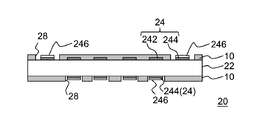
- FIG. 1 is a schematic diagram illustrating an example of a structure of a circuit board 20 in the embodiment.
- the circuit board of the present embodiment can include a substrate 22 formed on the surface of the circuit (conductor pattern 24) and a solder resist 10 formed on the outermost layer on the surface of the substrate.
- the said soldering resist is comprised with the hardened
- the film thickness of a soldering resist can be made into the same range as the film thickness of the said resin layer which is 1 micrometer or more and 50 micrometers or less, for example.
- the storage elastic modulus at 30 ° C. of the solder resist can be in the same range as the cured product of the resin layer, for example, 7 GPa or more and 40 GPa or less.
- a circuit board 20 shown in FIG. 1 includes a board 22, a conductor pattern 24, and a solder resist 10.
- the conductor pattern 24 is provided on at least one outermost surface of the substrate 22.
- the solder resist 10 constitutes the outermost layer of the circuit board 20.
- the solder resist 10 is provided around the conductor pattern 24.
- the solder resist 10 is provided with a plurality of openings 28. A part of the conductive portion of the conductor pattern 24 is located in the at least one opening 28.
- the board 22 may be a board including at least one insulating layer.
- the insulating layer provided in the substrate 22 is a resin base material obtained by impregnating a fiber base material with a resin composition, for example.
- substrate 22 may be a board
- the substrate 22 may be made of a thermosetting resin.
- the substrate 22 may be a rigid substrate or a flexible substrate.
- the lower limit value of the film thickness of the substrate 22 is not particularly limited, but may be, for example, 10 ⁇ m or more, 15 ⁇ m or more, or 30 ⁇ m or more. Thereby, it can be set as the circuit board excellent in mechanical strength.
- the upper limit value of the film thickness of the substrate 22 is, for example, 100 ⁇ m or less, preferably 80 ⁇ m or less, and more preferably 70 ⁇ m or less. Thereby, the circuit board 20 can be sufficiently thinned.
- the circuit board 20 of the present embodiment may have a structure in which the solder resist 10 is formed on at least one surface of the substrate 22, and more preferably has a structure in which the solder resist 10 is formed on both surfaces of the substrate 22.
- the total film thickness of the substrate 22 and the solder resist 10 is, for example, preferably 200 ⁇ m or less, more preferably 150 ⁇ m or less, and further preferably 100 ⁇ m or less.
- the lower limit of the film thickness ratio of the solder resist 10 to the total film thickness is, for example, 10% or more, preferably 20% or more, and more preferably 30% or more.
- the upper limit of the film thickness ratio is, for example, 70% or less, preferably 60% or less, and more preferably 50% or less.
- the substrate 22 may be a single-sided plate having only one insulating layer and having a conductor pattern 24 formed on only one side thereof, or having only one layer and having a conductor on both the front and back surfaces.
- a double-sided board provided with the pattern 24 may be used, or a multilayer board having two or more insulating layers may be used.
- the substrate 22 is a multilayer board, one or more wiring layers sandwiched between two insulating layers are formed in the substrate 22.
- the conductor pattern 24 provided on one surface (outermost surface) of the substrate 22 is the conductor pattern 24 provided on the opposite surface (outermost surface).
- a wiring layer provided inside the substrate 22 and electrically connected to each other through a through hole (not shown) penetrating at least a part of the insulating layer.
- the conductor pattern 24 is provided on at least one surface (outermost surface) of the front surface and the back surface of the substrate 22.
- the conductor pattern 24 is, for example, a pattern formed by selectively etching a copper film laminated on the substrate 22.
- the conductor pattern 24 includes at least a land 244 and a line 242 as a conductive portion.
- the land 244 is mainly a connection part that electrically connects an element or a component mounted on the circuit board 20 and the conductor pattern 24, for example, to another part of the conductor pattern 24 or a wiring layer in the board 22. It is a connected circular or square part. Note that a hole for inserting a terminal of an electronic component or the like may be provided at the center of the land 244.
- the line 242 is mainly a linear portion that electrically connects the lands 244 to each other.
- the solder resist 10 is laminated on the conductor pattern 24. Thereby, since insulation can be maintained, a highly reliable circuit board can be obtained. Moreover, since the said soldering resist is arrange
- the solder resist 10 is provided with an opening 28 mainly in a region where the land 244 is provided, and the land 244 is not covered with the solder resist 10. That is, the solder resist 10 is not provided on the land 244 and the land 244 is exposed.
- a conductive film such as a nickel and gold plating film or a solder plating film may be laminated on the land 244.
- a plating film 246 is further provided on the land 244 located in the opening 28.
- the solder resist 10 may be further provided with an opening in a portion other than the land 244, or may have an opening 28 that exposes a part of the line 242. Further, it is not necessary for all of the lands 244 to be located in the opening 28, and there may be lands 244 covered with the solder resist 10.
- the circuit board 20 of the present embodiment can be used as an interposer or a motherboard, for example.
- the package refers to a package in which various parts are mounted on a circuit board and collectively sealed.
- the semiconductor package is an example of a package, and the package includes a batch sealed ECU (Electric Control Unit) and the like.
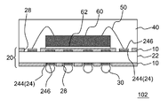
- FIG. 2 is a schematic cross-sectional view showing an example of the structure of the semiconductor package 102 according to this embodiment.
- the electronic device (semiconductor package 102) of the present embodiment can include the circuit board (circuit board 20) and an electronic element (semiconductor element 60) mounted on the circuit board. That is, the electronic device can be used as a semiconductor device.
- the solder resists constituting the outermost layer of the circuit board the solder resist (the solder resist 10 on the lower layer side) disposed on the surface opposite to the surface on which the electronic elements are mounted is the solder resist of this embodiment. It can be obtained by curing the resin composition.
- the semiconductor package 102 shown in FIG. 2 includes a circuit board 20, a semiconductor element 60, and a sealing resin layer 40.
- the semiconductor element 60 is disposed on the circuit board 20.
- the sealing resin layer 40 covers at least one surface of the circuit board 20 and the semiconductor element 60.
- the circuit board 20 includes a substrate 22, a conductor pattern 24, and the solder resist 10.
- the conductor pattern 24 is provided on at least one outermost surface of the substrate 22.
- the solder resist 10 is the outermost layer of the circuit board 20 and is provided around the conductor pattern 24.
- the semiconductor package 102 at least one semiconductor element 60 is disposed on the solder resist 10 on one surface (hereinafter referred to as “upper surface”) of the circuit board 20 described above.
- the circuit board 20 is, for example, an interposer
- the semiconductor element 60 is, for example, an LSI chip cut out from a semiconductor wafer.
- an electronic component that functions as a resistor or a capacitor may be further disposed on the upper surface of the circuit board 20.
- the semiconductor element 60 is fixed on the solder resist 10 via a die attach material 62.
- the semiconductor element 60 is provided with an electrical connection pad (not shown) on its surface, and the connection pad is connected to a circuit built in the semiconductor element 60, for example.
- a land 244 that is a part of the conductor pattern 24 provided on the circuit board 20 is provided in the opening 28 of the solder resist 10.
- the land 244 and the connection pad of the semiconductor element 60 are connected by a bonding wire 50.
- the plating film 246 is further provided on the land 244, and the land 244 is connected to the bonding wire 50 through the plating film 246.
- the present invention is not limited to this. . Further, instead of being connected by the bonding wire 50, it may be connected by a lead wire or solder.
- the sealing resin layer 40 includes a solder resist 10 exposed on the upper surface of the circuit board 20, the substrate 22, a plating film 246 (land 244 if no plating film 246 is provided), and die attach among the semiconductor elements 60.
- the material 62 covers the surface other than the surface bonded to the circuit board 20 and the bonding wire 50.
- the sealing resin layer 40 may cover the entire surface of the circuit board 20 on which the semiconductor element 60 is provided, or may cover a part of the surface exposed.
- the circuit board 20 of the semiconductor package 102 is further provided with a plurality of openings 28 and lands 244 inside the openings 28 on a surface opposite to the upper surface (hereinafter referred to as “lower surface”). Each land 244 is covered with a plating film 246, and further solder balls 30 are provided to cover the plating film 246.
- a flip chip connection package has been described as the semiconductor package 102 according to the present embodiment, but the present invention is not limited to this, and a package that is connected by wire bonding or TAB (Tape Automated Bonding) may be used.
- the sealing resin layer 40 of the electronic device and the lower solder resist 10 (solder resist of the present embodiment) disposed on the side opposite to the mounting surface can be the same color.
- each can be the same or similar black.
- a black seal that covers the external connection electrodes may be attached to the lower surface of the solder resist 10 in the lower layer of the electronic device.
- a mark is printed on the upper surface of the sealing resin layer 40 or the lower surface of the solder resist 10 by a laser such as a YAG laser, for example.
- This mark is made up of, for example, at least one of letters, numbers, or symbols consisting of straight lines or curves.
- the mark indicates, for example, the product name, product number, lot number, or manufacturer name of the semiconductor package.
- the mark may be stamped by, for example, a YVO 4 laser, a carbonic acid laser, or the like.
- the electronic device is not particularly limited.
- QFP Quad Flat Package
- SOP Small Outline Package
- BGA Bit Grid Array
- CSP Chip Size Package
- QFN Quad Flat Flat
- lead Package SON (Small Outline Non-leaded Package), LF-BGA (Lead Frame BGA), and the like.
- examples of the semiconductor element include, but are not limited to, an integrated circuit, a large-scale integrated circuit, a transistor, a thyristor, a diode, and a solid-state imaging element.
- the manufacturing method of the circuit board 20 includes a step of preparing the substrate 22, a step of laminating a resin layer, a step of forming the opening 28, and a step of desmear treatment in this order.
- the substrate 22 having the conductor pattern 24 provided on at least one outermost surface is prepared.
- the outermost resin layer is laminated on the substrate 22 and the conductor pattern 24.
- a part of the conductor pattern 24 is exposed in a predetermined region of the resin layer.
- the surface of the resin layer is desmeared.
- the step of forming the opening 28 includes a step of irradiating a region of the resin layer that is to be the opening 28 with laser light.
- a substrate 22 having a conductor pattern 24 provided on at least one outermost surface of the front and back is prepared (step of preparing a substrate).
- a resin layer is laminated on the conductor pattern 24 of the substrate 22 (stacking step).
- a resin sheet is pasted on the surface of the substrate 22 on which the conductor pattern 24 is provided so that the resin layer faces the substrate 22.
- the resin sheet can be attached by, for example, laminating a resin layer of the resin sheet on the conductor pattern 24 and then vacuum-pressing the resin layer.
- the resin sheet may be a resin layer with a metal foil or a resin layer with a resin film.
- the carrier substrate is peeled from the resin layer. As a result, a resin layer is formed on the substrate 22 so as to cover the conductor pattern 24.
- an opening 28 is provided at a predetermined position of the resin layer on the conductor pattern 24 (step of forming an opening).
- the opening 28 is formed so as to mainly expose the land 244 of the conductor pattern 24.
- a method for forming the opening 28 is not particularly limited, and a method such as an exposure development method or a laser processing method can be used.
- the solder resist resin composition needs to contain a photosensitizer.
- the exposure and development method first, exposure is performed by selectively irradiating light to either the region where the opening 28 is formed or the region where the opening 28 is not formed in the resin layer. Thereafter, the opening 28 can be formed by performing development using a developer such as an alkaline aqueous solution.
- the B-stage resin layer is thermally cured to form a solder resist 10 (cured product of the resin layer).
- the curing temperature is not particularly limited, but may be, for example, 160 ° C. or higher, 180 ° C. or higher, or 200 ° C. or higher.
- the solder resist 10 solder resist
- the exposure for example, a method of irradiating ultraviolet rays with a mask pattern adhered, or a method of directly irradiating a desired region with laser light can be used.
- the step of forming the opening 28 there is a method of irradiating a region to be the opening 28 in the resin layer with a laser beam (a step of irradiating the laser beam) to form the opening.
- the laser processing method is more preferable.
- desmear treatment can be performed as necessary (desmear treatment step). In the desmear process, smear generated due to the formation of the opening 28 is removed.
- the plating film 246 is formed on the conductor pattern 24 exposed in the opening 28 after forming the opening 28 and performing desmear treatment as necessary. Plating is performed.
- the circuit board 20 may be formed without forming the plating film 246.
- the plating film 246 can be, for example, a plating film having a two-layer structure in which a gold plating film is laminated on a solder plating film, a tin plating film, or a nickel plating film.
- the plating film 246 is formed so as to cover the conductive portion of the conductor pattern 24 exposed in the opening 28.
- the film thickness of the plating film 246 is not particularly limited, but may be, for example, 2 ⁇ m or more and 10 ⁇ m or less.
- the land 244 portion can be used as a bonding wire 50 or a connection portion suitable for soldering in the mounting process using the circuit board 20.
- the method for the plating treatment is not particularly limited, and a known method can be used.
- an electrolytic plating method or an electroless plating method can be used.
- the plating film 246 can be formed as follows.
- an example of forming the plating film 246 having a two-layer structure of nickel and gold will be described, but the present invention is not limited to this.
- a nickel plating film is formed.
- stacked the conductor pattern 24 and the soldering resist 10 on the plating solution is immersed.
- a nickel plating film can be formed on the conductive portion of the conductor pattern 24 exposed at the opening 28.
- nickel lead and a reducing agent containing, for example, hypophosphite can be used as the plating solution.
- electroless gold plating is performed on the nickel plating film.
- the method of electroless gold plating is not particularly limited, for example, it can be performed by substitution gold plating performed by substitution of gold ions and ions of a base metal.
- the surface on which the solder resist 10 is formed may be subjected to plasma treatment. As described above, the circuit board 20 according to the present embodiment as shown in FIG. 1 is obtained.
- a step of preparing a substrate (substrate 22) having a conductive circuit (conductor pattern 24) formed on one surface, and the resin layer are disposed on the substrate.
- the step of electrically connecting to the circuit and the step of sealing the electronic element (semiconductor element 60) can be included.
- the manufacturing method of the semiconductor package 102 includes a step of preparing the circuit board 20, a step of disposing the semiconductor element 60, and a step of sealing in this order.
- the step of preparing the circuit board 20 the circuit board 20 having the solder resist 10 (solder resist) exposed on the surface is prepared.
- the step of disposing the semiconductor element 60 the semiconductor element 60 is disposed on the solder resist 10.
- the sealing step the exposed solder resist 10 and the semiconductor element 60 are sealed so as to be covered with a sealing resin.
- the circuit board 20 includes a substrate 22, a conductor pattern 24, and the solder resist 10.
- the conductor pattern 24 is provided on at least one outermost surface of the substrate 22.
- the solder resist 10 is the outermost layer of the circuit board 20 and is provided on the conductor pattern 24.
- the solder resist 10 is provided with a plurality of openings 28. A part of the conductive portion of the conductor pattern 24 is located in the at least one opening 28.
- the above-described circuit board 20 is prepared (step of preparing a circuit board), and the semiconductor element 60 is disposed on the circuit board 20 (step of disposing the semiconductor element).
- the semiconductor element 60 is mounted on the circuit board 20 via a die attach material 62, for example.
- the bonding wire 50 that connects the semiconductor element 60 and the circuit board 20 is bonded to, for example, the conductor pattern 24 exposed in the opening 28 on the upper surface of the circuit board 20.
- the upper surface of the circuit board 20, the semiconductor element 60, and the bonding wire 50 are sealed with the sealing resin layer 40 (step of sealing).
- an epoxy resin composition can be used as the sealing resin.
- a transfer molding method As a method of molding with a sealing resin, a transfer molding method, an injection molding method, a transfer method, a coating method, or the like can be used.
- the sealing resin layer 40 is cured by heating at 150 ° C. or higher and 200 ° C. or lower, for example.
- solder balls 30 as external connection terminals are provided on the circuit board 20
- the solder balls 30 are formed on the conductor pattern 24 exposed at the opening 28 on the lower surface side.
- the semiconductor package 102 is not limited to this, The package connected by wire bonding or TAB may be sufficient.
- a carrier substrate A resin sheet used for a solder resist, comprising a resin layer disposed on the carrier substrate and comprising a resin composition for a solder resist,
- the resin layer has a thickness of 1 ⁇ m or more and 50 ⁇ m or less, When the minimum value of the complex dynamic viscosity in a measurement range of 50 to 200 ° C., a temperature increase rate of 3 ° C./min, and a frequency of 62.83 rad / sec is ⁇ by the dynamic viscoelasticity test in the B stage state of the resin layer.
- ⁇ is 100 Pa ⁇ s or more and 3000 Pa ⁇ s or less
- cured material of the said resin layer is 7 GPa or more and 40 GPa or less.
- the resin sheet according to claim 1 The resin sheet whose glass transition temperature of the hardened
- the resin sheet according to claim 1 The resin sheet whose linear expansion coefficient in less than the glass transition temperature of the hardened
- cured material of the said resin layer is 0.2 GPa or more and 10 GPa or less. 5. 1. To 4. The resin sheet according to any one of The resin sheet whose resin flow amount of the B stage state of the said resin layer measured on condition of the following is 5 weight% or more and less than 70 weight%.
- the resin sheet according to claim 1 The resin sheet in which the thermosetting resin contains an epoxy resin. 9. 7). Or 8. The resin sheet according to claim 1, A resin sheet in which the filler contains silica. 10. 7). To 9. The resin sheet according to any one of The resin sheet for the solder resist resin composition further comprising a cyanate resin. 11. 1. To 10. The resin sheet according to any one of The resin sheet whose deflection amount measured on condition of the following is less than 35 mm. (Measurement conditions of deflection) After the solder resist resin composition is applied to the carrier substrate, the solvent is removed at 140 ° C. for 2 minutes to form a resin layer having a thickness of 20 ⁇ m.
- a double-sided copper clad laminate is prepared by laminating a 12 ⁇ m thick copper foil on one side and the other side of a core substrate (50 mm ⁇ 85 mm, 30 ⁇ mt). Next, the copper foil of the double-sided copper-clad laminate is etched to obtain a substrate from which the copper foil has been removed. Next, after laminating the resin sheet on each of the one surface and the other surface of the substrate so that the resin layer faces the substrate, the temperature is 120 ° C. and the pressure is 0.8 MPa using a vacuum pressure laminator device. And vacuum heating and pressure molding under the condition of 120 seconds. Next, after peeling the carrier base material from the resin sheet, the resin layer on the substrate was cured at 200 ° C.
- the deflection amount of the other side is measured in a state where the other side facing the one side is a free end while supporting 10 mm from the end of the one side which is the short side.
- the solder resist is composed of a cured product of a resin layer made of a resin composition for solder resist, The resin layer has a thickness of 1 ⁇ m or more and 50 ⁇ m or less, The circuit board whose storage elastic modulus in 30 degreeC of the hardened
- the circuit board according to claim 1 The circuit board whose total value of the film thickness of the said board
- Thermosetting resin Thermosetting resin 1: naphthol type epoxy resin (Nippon Kayaku Co., Ltd., NC-7000L)
- Thermosetting resin 2 Bifunctional naphthalene type epoxy resin (manufactured by DIC, HP-4032D)
- Thermosetting resin 3 Epoxy acrylate resin (manufactured by Nippon Kayaku Co., Ltd., ZFR-1401)
- Thermosetting resin 4 Biphenyl dimethylene type epoxy resin (Nippon Kayaku Co., Ltd., NC-3000L)
- Acrylic monomer 1 Bifunctional ethoxylated bisphenol A dimethacrylate (manufactured by Shin-Nakamura Chemical Co., BPE-500)
- Acrylic monomer 2 Bifunctional urethane acrylate (Nippon Kayaku Co., Ltd.,
- Examples 1-3 Preparation of varnish of resin composition
- epoxy resin naphthol type epoxy resin (Nippon Kayaku Co., Ltd., NC-7000L) 10.0 parts by weight, bifunctional naphthalene type epoxy resin (DIC, HP-4032D) 3.6 parts by weight, novolak phenol type cyanate 13.6 parts by weight of an ester resin (Lonza Japan, PT-30), spherical silica (Admatex, SC4050) having an average particle diameter D 50 of 1 ⁇ m, 72 parts by weight, tetraphenylphosphonium bis (naphthalene) -2,3-dioxy) phenylsilicate adduct 0.3 parts by weight, epoxysilane (manufactured by Shin-Etsu Chemical Co., Ltd., KBM-403) 0.2 parts by weight, and leveling agent (manufactured by BYK Japan Japan, BYK-356) Dissolve and disperse 0.3 parts by weight in
- Example 4 Preparation of varnish of resin composition
- an epoxy resin 16.5 parts by weight of a naphthol type epoxy resin (manufactured by Nippon Kayaku Co., Ltd., NC-7000L), 5.5 parts by weight of a bifunctional naphthalene type epoxy resin (manufactured by DIC, HP-4032D), a novolak phenol type cyanate ester resin (Lonza Japan Ltd., PT-30) 22.0 parts by weight, average particle diameter D 50 0.5 ⁇ m spherical silica (Admatechs Co., SC2050) 55 parts by weight solids, bis tetraphenylphosphonium 0.44 parts by weight of (naphthalene-2,3-dioxy) phenyl silicate adduct, 0.12 parts by weight of epoxysilane (manufactured by Shin-Etsu Chemical Co., Ltd., KBM-403), and leveling agent (manufactured by BYK Japan, B
- Example 5 Preparation of varnish of resin composition
- a resin composition varnish was prepared in the same manner as in Example 1 using the components shown in Table 1.
- Example 7 Preparation of varnish of resin composition
- an epoxy resin naphthol type epoxy resin (Nippon Kayaku Co., Ltd., NC-7000L) 20.2 parts by weight, biphenyldimethylene type epoxy resin (Nippon Kayaku Co., Ltd., NC-3000L) 6.7 parts by weight, novolak phenol Type cyanate ester resin (manufactured by Lonza Japan, PT-30) 26.9 parts by weight, spherical silica (manufactured by Admatechs, SC2050, average particle size D 50 : 0.5 ⁇ m) solid content 45 parts by weight, tetraphenylphosphonium Bis (naphthalene-2,3-dioxy) phenylsilicate adduct (Sumitomo Bakelite Co., Ltd., C05-MB) 0.53 parts by weight, epoxysilane (Shin-Etsu Chemical Co., Ltd., KBM-403) 0.14 parts by weight, And 0.
- Example 8 Preparation of varnish of resin composition
- an epoxy resin 16.5 parts by weight of a naphthol type epoxy resin (manufactured by Nippon Kayaku Co., Ltd., NC-7000L), 5.5 parts by weight of a bifunctional naphthalene type epoxy resin (manufactured by DIC, HP-4032D), a novolak phenol type cyanate Ester resin (manufactured by Lonza Japan, PT-30) 22 parts by weight, spherical silica (manufactured by Admatechs, SC4050, average particle size D 50 : 1 ⁇ m) solid content 30 parts by weight, spherical silica (manufactured by Admatechs, SC2050) , Average particle diameter D 50 : 0.5 ⁇ m) 25 parts by weight of solid content, bis (naphthalene-2,3-dioxy) phenylsilicate adduct of tetraphenylphosphonium (
- Epoxy acrylate resin (Nippon Kayaku Co., Ltd., ZFR-1401) 45.8 parts by weight, epoxy resin biphenyldimethylene type epoxy resin (Nippon Kayaku Co., Ltd., NC-3000L) 14.8 parts by weight, photoreaction initiator 2.9 parts by weight of 2,4,6-trimethylbenzoyl-diphenyl-phosphine oxide (manufactured by BASF Japan, TPO), 2-benzyl-2-dimethylamino-1- (4-morpholinophenyl) -butanone -1 (manufactured by BASF Japan, Irgacure 369) 0.15 parts by weight, oxime compound (manufactured by BASF Japan, OXE-02) 0.06 parts by weight, bifunctional ethoxylated bisphenol A dimethacrylate (manufactured by Shin-Nakamura Chemical Co., Ltd.) BPE-500) 4.54 parts
- the lowest complex dynamic viscosity (minimum value of complex viscosity) was measured as follows. First, based on the production of the resin sheet, a resin sheet having a resin layer having a resin thickness of 20 ⁇ m was obtained. Next, from the obtained resin sheet, five resin layers (films) from which the PET film as a carrier substrate was peeled were overlapped to prepare a measurement sample having a total film thickness of 100 ⁇ m. Subsequently, the complex dynamic viscosity was measured on the measurement sample under the following conditions using a dynamic viscoelasticity measuring apparatus (manufactured by Anton Paar, apparatus name Physica MCR-301).
- the resin sheet in which the resin layer which has a resin thickness of 20 micrometers was formed based on preparation of the said resin sheet was obtained.
- five resin layers (films) from which the PET film as a carrier substrate was peeled were overlapped to prepare a laminated film having a total film thickness of 100 ⁇ m.
- the laminated film was heat-treated at 200 ° C. for 1 hour, and then cut into a width of 8 mm ⁇ a length of 50 mm ⁇ a thickness of 100 ⁇ m to obtain a measurement sample.
- a dynamic viscoelasticity test was performed on the measurement sample using a dynamic viscoelasticity measurement apparatus (Seiko Instruments, DMS6100) under conditions of a frequency of 1 Hz and a temperature increase rate of 5 ° C./min.
- the glass transition temperature (° C.), the storage elastic modulus (GPa) at 30 ° C., and the storage elastic modulus (GPa) at 260 ° C. were calculated from the obtained measurement results.
- the glass transition temperature was determined from the peak value of tan ⁇ . The results are shown in Table 1.
- the resin sheet in which the resin layer which has a resin thickness of 20 micrometers was formed based on preparation of the said resin sheet was obtained.
- five resin layers (films) from which the PET film as a carrier substrate was peeled were overlapped to prepare a laminated film having a total film thickness of 100 ⁇ m.
- the laminated film was heat treated at 200 ° C. for 1 hour, and then cut into a width of 4 mm ⁇ a length of 20 mm ⁇ a thickness of 100 ⁇ m to obtain a measurement sample.
- the linear expansion coefficient was measured on the measurement sample using TMA (manufactured by TA Instruments Co., Ltd.) under the condition of a temperature increase rate of 10 ° C./min. Next, the average of the measurement results at 50 to 75 ° C. was calculated, and this was taken as the linear expansion coefficient (ppm / ° C.) below the glass transition temperature. The results are shown in Table 1.
- a double-sided copper-clad laminate is prepared by laminating 12 ⁇ m thick copper foil on one side and the other side of the core substrate (LAZ-4785TH-G, manufactured by Sumitomo Bakelite Co., Ltd., 50 mm x 85 mm, film thickness shown in Table 1) did. Subsequently, the copper foil of the said double-sided copper clad laminated board was etched, and the board
- a temperature of 120 ° C. and a pressure using a vacuum pressure laminator device Vacuum heating and pressure molding is performed under the conditions of 0.8 MPa and 120 seconds.
- the resin layer on the substrate was cured at 200 ° C. for 1 hour to form a solder resist. In this way, a sample is obtained.
- a film conveyance pressurization type vacuum laminator (Miki Seisakusho make, MVLP500 / 600) evaluated conveyance property.
- the evaluation method is as follows: From the set position of the substrate at the start of conveyance, the positional displacement of the four corners of the substrate after 30 seconds after vacuum as 0.5 MPa as the primary pressurization and after 30 seconds at 0.5 MPa as the second pressurization The maximum amount was measured. Criteria for transportability: ⁇ : 15 mm or less ⁇ : larger than 15 mm
- the semiconductor package was produced as follows. First, a double-sided copper-clad laminate in which a 12 ⁇ m-thick copper foil was laminated on one side and the other side of a 30 ⁇ m-thick core substrate (LAZ-4785TH-G, manufactured by Sumitomo Bakelite Co., Ltd.) was prepared. Subsequently, the copper foil of the said copper clad laminated board was etched, and the conductor circuit pattern was formed, and the circuit board by which the said conductor circuit pattern was formed in the one surface and the other surface was obtained.
- LAZ-4785TH-G manufactured by Sumitomo Bakelite Co., Ltd.
- a vacuum pressurization method is performed. Using a laminator apparatus, vacuum heating and pressing were performed under the conditions of a temperature of 120 ° C., a pressure of 0.8 MPa, and 60 seconds. Next, after peeling the PET film as the carrier substrate from the resin sheet, the resin layer on the circuit board was cured at 200 ° C. for 1 hour to form a solder resist.
- an opening is formed in a solder resist provided on one surface of the circuit board by a carbonic acid laser so that a part of the conductor circuit pattern is exposed, and then desmear treatment and plasma treatment are performed on the one surface of the circuit board. did.
- the conductor pattern exposed from the opening and the semiconductor element were connected by a bonding wire.
- the semiconductor element and the bonding wire were encapsulated with an epoxy resin composition to obtain a semiconductor package (16 mm ⁇ 16 mm).
- the curvature amount in 25 degreeC of the obtained semiconductor package was measured.
- the package warpage was evaluated by setting the case where the package warpage amount was less than 150 ⁇ m as ⁇ and the case where the package warpage amount was 150 ⁇ m or more as x.
- the package warpage amount is defined by the distance between the center point of the upper surface of the semiconductor package and the outer peripheral portion of the upper surface in the stacking direction of the semiconductor element and the circuit board.
Landscapes
- Chemical & Material Sciences (AREA)
- Health & Medical Sciences (AREA)
- Chemical Kinetics & Catalysis (AREA)
- Medicinal Chemistry (AREA)
- Polymers & Plastics (AREA)
- Organic Chemistry (AREA)
- Engineering & Computer Science (AREA)
- Manufacturing & Machinery (AREA)
- Microelectronics & Electronic Packaging (AREA)
- Non-Metallic Protective Coatings For Printed Circuits (AREA)
- Materials Engineering (AREA)
- Compositions Of Macromolecular Compounds (AREA)
Abstract
Description
(1)現在、プリント配線板などの回路基板において、薄層化が進んで来ている。薄層化に伴い、回路基板に生じるたわみが顕在化してきた。たわみが回路基板に生じると、実装プロセス中において、基板の搬送が困難になること等の搬送信頼性が低下することが判明した。たとえ基板自体を剛性化する手法を採用したとしても、たわみの抑制は十分ではなかった。
(2)このように顕在化した基板のたわみに対して、各種の検討を行った結果、基板の表面に形成されるソルダーレジスト(樹脂フィルムの硬化物)の剛性を高めることで、基板のたわみを十分に抑制できることを見出した。詳細なメカニズムは定かでないが、基板表面に形成されたソルダーレジストの剛性を高めることで、吊り橋構造のように基板を引っ張り上げることができるため、基板搬送時における、基板自体の剛性を高める以上の剛性構造を生み出し、基板のたわみを抑制できると考えられる。
(3)剛性に優れたソルダーレジストについて更なる検討を行った結果、当該ソルダーレジストを構成する樹脂層を硬化する前、かかる樹脂層を基板表面の配線に埋め込むとき、Bステージ状態(半硬化物)である樹脂層において樹脂流れが生じることがあることが判明した。
また、樹脂層のBステージ状態の特性について検討を深めた結果、測定範囲50~200℃における、複素動的粘度の極小値を指標とすることにより、基板表面に形成された配線に樹脂層を埋め込む際に、当該樹脂層が基板の外部に流れ出る樹脂について安定的に評価できることを見出した。
本発明者は、以上の知見に基づいて鋭意検討した所、ソルダーレジストに用いる樹脂フィルムについて、30℃における貯蔵弾性率を所定値以上とし、複素動的粘度の極小値を所定値以上とすることにより、基板の外部に流出せずに残存したソルダーレジストの剛性を高めることができるため、基板搬送時における基板のたわみを十分に抑制できる剛性構造を実現でき、搬送信頼性を向上させることができることを見出し、本発明を完成するに至った。
キャリア基材と、
前記キャリア基材上に配置されていて、ソルダーレジスト用樹脂組成物からなる樹脂層と、を備える、ソルダーレジストに用いる樹脂シートであって、
前記樹脂層の膜厚が、1μm以上50μm以下であり、
前記樹脂層のBステージ状態の動的粘弾性試験による、測定範囲50~200℃、昇温速度3℃/min、周波数62.83rad/secでの複素動的粘度の極小値をηとしたとき、ηが、100Pa・s以上3000Pa・s以下であり、
前記樹脂層の硬化物の30℃における貯蔵弾性率が7GPa以上40GPa以下である、樹脂シートが提供される。
本実施形態の樹脂シートは、キャリア基材と、キャリア基材上に配置されており、ソルダーレジスト用樹脂組成物からなる樹脂層と、を備えるものである。当該樹脂シートは、ソルダーレジストに用いるものである。
また、本実施形態の樹脂シートは、次のような条件を満たすものである。
・樹脂層の膜厚が、1μm以上50μm以下であること。
・樹脂層のBステージ状態の動的粘弾性試験による、測定範囲50~200℃、昇温速度3℃/min、周波数62.83rad/secでの複素動的粘度の極小値をηとしたとき、ηが、100Pa・s以上3000Pa・s以下であること。
・樹脂層の硬化物の30℃における貯蔵弾性率が7GPa以上40GPa以下であること。
以下、本実施形態の樹脂層に用いられるソルダーレジスト用樹脂組成物を説明する。
本実施形態のソルダーレジスト用樹脂組成物は、ワニス状の樹脂組成物である。当該ソルダーレジスト用樹脂組成物をフィルム状とすることにより、本実施形態の樹脂層を得ることができる。かかる樹脂層を硬化させることにより、ソルダーレジストが得られる。
本実施形態に係るエポキシ樹脂(A)は、たとえばビスフェノールA型エポキシ樹脂、ビスフェノールF型エポキシ樹脂、ビスフェノールE型エポキシ樹脂、ビスフェノールS型エポキシ樹脂、ビスフェノールM型エポキシ樹脂(4,4’-(1,3-フェニレンジイソプリジエン)ビスフェノール型エポキシ樹脂)、ビスフェノールP型エポキシ樹脂(4,4’-(1,4-フェニレンジイソプリジエン)ビスフェノール型エポキシ樹脂)、ビスフェノールZ型エポキシ樹脂(4,4’-シクロヘキシジエンビスフェノール型エポキシ樹脂)などのビスフェノール型エポキシ樹脂;フェノールノボラック型エポキシ樹脂、クレゾールノボラック型エポキシ樹脂、テトラフェノール基エタン型ノボラック型エポキシ樹脂、縮合環芳香族炭化水素構造を有するノボラック型エポキシ樹脂などのノボラック型エポキシ樹脂;ビフェニル型エポキシ樹脂;キシリレン型エポキシ樹脂、ビフェニルアラルキル型エポキシ樹脂などのアラルキル型エポキシ樹脂;ナフチレンエーテル型エポキシ樹脂、ナフトール型エポキシ樹脂、ナフタレンジオール型エポキシ樹脂、2官能ないし4官能エポキシ型ナフタレン樹脂、ビナフチル型エポキシ樹脂、ナフタレンアラルキル型エポキシ樹脂、ナフタレン変性クレゾールノボラック型エポキシ樹脂などのナフタレン骨格を有するエポキシ樹脂;アントラセン型エポキシ樹脂;フェノキシ型エポキシ樹脂;ジシクロペンタジエン型エポキシ樹脂;ノルボルネン型エポキシ樹脂;アダマンタン型エポキシ樹脂;フルオレン型エポキシ樹脂等から選択される一種または二種以上を含むことができる。これらの中でも、ソルダーレジストの埋め込み性や、表面平滑性を向上させる観点からは、ナフタレン骨格を有するエポキシ樹脂を含むことがより好ましい。これにより、ソルダーレジストの低線膨張化および高弾性率化を図ることもできる。また、回路基板の剛性を向上させて作業性の向上に寄与することや、半導体パッケージにおける耐リフロー性の向上および反りの抑制を実現することも可能である。なお、ソルダーレジストの埋め込み性を向上させる観点からは、3官能以上のナフタレン骨格を有するエポキシ樹脂を含むことがとくに好ましい。

本実施形態のソルダーレジスト用樹脂組成物は、充填材をさらに含んでもよい。つまり、ソルダーレジスト用樹脂組成物は、熱硬化性樹脂と充填材とを含むことができる。
本実施形態に係る充填材としては、無機充填材を用いることができる。上記無機充填剤としては、特に限定されないが、例えば、タルク、焼成クレー、未焼成クレー、マイカ、ガラスなどのケイ酸塩;酸化チタン、アルミナ、ベーマイト、シリカ、溶融シリカなどの酸化物;炭酸カルシウム、炭酸マグネシウム、ハイドロタルサイトなどの炭酸塩;水酸化アルミニウム、水酸化マグネシウム、水酸化カルシウムなどの水酸化物;硫酸バリウム、硫酸カルシウム、亜硫酸カルシウムなどの硫酸塩または亜硫酸塩;ホウ酸亜鉛、メタホウ酸バリウム、ホウ酸アルミニウム、ホウ酸カルシウム、ホウ酸ナトリウムなどのホウ酸塩;窒化アルミニウム、窒化ホウ素、窒化ケイ素、窒化炭素などの窒化物;チタン酸ストロンチウム、チタン酸バリウムなどのチタン酸塩などを挙げることができる。これらの中でも、タルク、アルミナ、ガラス、シリカ、マイカ、水酸化アルミニウム、水酸化マグネシウムが好ましい。
本実施形態のソルダーレジスト用樹脂組成物は、シアネート樹脂(C)をさらに含むことができる。これにより、ソルダーレジストについて、低線膨張化や、弾性率および剛性の向上を図ることができる。また、得られる電子装置の耐熱性や耐湿性の向上に寄与することも可能である。
また、上記シアネート樹脂(C)は、特に限定されるものではないが、例えば、ハロゲン化シアン化合物と、フェノール類またはナフトール類と、を反応させて得ることができる。このようなシアネート樹脂としては、例えば、フェノールノボラック型の多価フェノール類とハロゲン化シアンとの反応で得られるシアネート樹脂、クレゾールノボラック型の多価フェノール類とハロゲン化シアンとの反応で得られるシアネート樹脂、ナフトールアラルキル型の多価ナフトール類とハロゲン化シアンとの反応で得られるシアネート樹脂などが挙げられる。上記シアネート樹脂は、一種または二種以上を組み合わせて用いてもよい。
これらの中でも、ソルダーレジストの低線膨張化や、弾性率および剛性を向上させる観点からは、フェノールノボラック型シアネートエステル樹脂、ジシクロペンタジエン型シアネートエステル樹脂、またはナフトールアラルキル型シアネート樹脂を含むことがより好ましく、フェノールノボラック型シアネートエステル樹脂を含むことがとくに好ましい。
本実施形態のソルダーレジスト用樹脂組成物は、たとえば硬化促進剤(D)をさらに含むことができる。これにより、ソルダーレジスト用樹脂組成物の硬化性を向上させることができる。
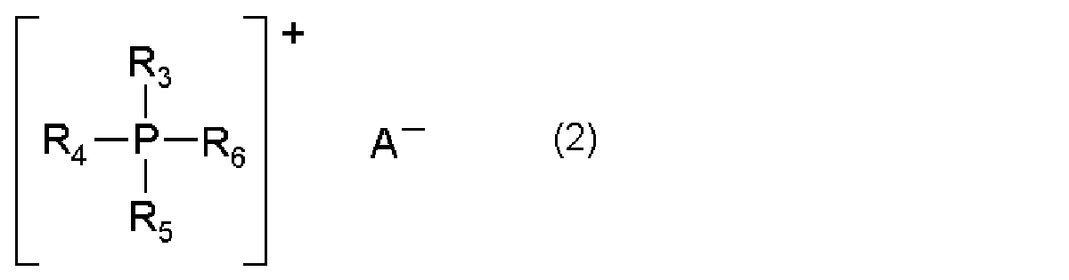
本実施形態のソルダーレジスト用樹脂組成物は、たとえば、着色剤(E)をさらに含むことができる。本実施形態の着色剤(E)は、たとえば緑、赤、青、黄、および黒等の染料、顔料、および色素から選択される一種または二種以上を含む。これらの中でも、開口部の視認性等を向上させる観点から、緑色の着色剤を含むことができるが、緑色染料を含めてもよい。当該緑色の着色剤としては、たとえばアントラキノン系、フタロシアニン系、およびペリレン系等の公知の着色剤を一種または二種以上含むことができる。
本実施形態のソルダーレジスト用樹脂組成物には、上記各成分以外に、必要に応じてカップリング剤、レベリング剤、硬化剤、感光剤、消泡剤、紫外線吸収剤、発泡剤、酸化防止剤、難燃剤、およびイオン捕捉剤等から選択される一種または二種以上の添加物を添加してもよい。
上記レベリング剤としては、アクリル系共重合物等が挙げられる。
本実施形態に係る樹脂シートは、キャリア基材と、キャリア基材上に形成された樹脂層とを備えることができる。本実施形態の樹脂層は、Bステージ状態であり、上記のソルダーレジスト用樹脂組成物の乾燥フィルムで構成される。本実施形態における樹脂シートは、シート形状(枚葉形状)でもよく、巻き取り可能なロール形状でもよい。
上記樹脂ワニスにおいて、ソルダーレジスト用樹脂組成物の固形分含有量は、たとえば30重量%以上80重量%以下であることが好ましく、40重量%以上70重量%以下であることがより好ましい。これにより、作業性や成膜性に非常に優れたソルダーレジスト用樹脂組成物が得られる。なお、ワニス状のソルダーレジスト用樹脂組成物は、たとえば上述の各成分を、超音波分散方式、高圧衝突式分散方式、高速回転分散方式、ビーズミル方式、高速せん断分散方式、および自転公転式分散方式などの各種混合機を用いて溶剤中に溶解、混合、撹拌することにより調製することができる。
本実施形態の溶剤としては、たとえばアセトン、メチルエチルケトン、メチルイソブチルケトン、トルエン、酢酸エチル、シクロヘキサン、ヘプタン、シクロヘキサン、シクロヘキサノン、テトラヒドロフラン、ジメチルホルムアミド、ジメチルアセトアミド、ジメチルスルホキシド、エチレングリコール、セルソルブ系、カルビトール系、アニソール、およびN-メチルピロリドン等の有機溶剤から選択される一種または二種以上を含むことができる。
本実施形態において、上記ηの下限値は、例えば、100Pa・s以上であり、好ましくは150Pa・s以上であり、より好ましくは200Pa・s以上である。これにより、樹脂層を基板に貼り付けた後の樹脂流れを抑制することができるため、ハンドリング性の向上を実現できる。また、上記ηの上限値は、特に限定されないが、例えば、3000Pa・s以下であり、好ましくは2500Pa・s以下であり、より好ましくは2000Pa・s以下である。これにより、樹脂層の埋め込み性を高めることができる。つまり、基板表面に形成された配線への埋め込みが容易になり、基板と樹脂層との密着性が安定して得られる。また、ハンドリング性の向上を実現できる。
周波数:62.83rad/sec
測定温度:50~200℃、昇温速度3℃/min
ジオメトリー:パラレルプレート
プレート直径:10mm
荷重(ノーマルフォース):0N(一定)
ストレイン:0.3%
測定雰囲気:空気
・サンプルサイズ113mmφで基材ごと打ち抜く
・基材つきのまま4枚重ね(W0)
・温度171±3℃、圧力750±50kPaの条件で加熱加圧
・113mmφからはみ出した樹脂を除いた重量を測定(W1)
(W0-W1)/(W0-基材重量)×100
また、本実施形態において、ガラス転移温度未満における貯蔵弾性率に対するガラス転移温度以上における貯蔵弾性率の貯蔵弾性率比は、次のように表すことができる。
貯蔵弾性率比=30℃における貯蔵弾性率/(260℃における貯蔵弾性率×10)
本実施形態における貯蔵弾性率比の上限値は、例えば、5.0以下としてもよく、より好ましくは0.90以下、特に好ましくは0.8以下、最も好ましくは0.7以下としてもよい。これにより、繰り返し熱履歴が加えられる使用環境においても、本実施形態の樹脂層の硬化物からなるソルダーレジストを備える回路基板のたわみを十分に抑制することができる。また、上記貯蔵弾性率比の下限値は、特に限定されないが、例えば、0.1以上としてもよく、0.3以上としてもよく、0.4以上としてもよい。これにより、搬送信頼性およびハンドリング性のバランスを図ることができる。
また、測定条件によるバラツキを抑制する観点から、本実施形態におけるたわみ量の測定条件としては、例えば、樹脂層の厚さが20μmかつ、コア基材の厚さが30μmである条件を採用することができる。
本実施形態に係る回路基板について説明する。
図1は、実施形態における回路基板20の構造の例を示す模式図である。
本実施形態の回路基板は、表面に回路(導電体パターン24)に形成された基板22と、基板の表面上である最外層に形成されたソルダーレジスト10と、を含むことができる。当該ソルダーレジストは、本実施形態のソルダーレジスト用樹脂組成物からなる樹脂層の硬化物で構成されている。
また、ソルダーレジストの膜厚は、たとえば1μm以上50μm以下である、上記樹脂層の膜厚と同様の範囲とすることができる。ソルダーレジストの30℃における貯蔵弾性率は、たとえば7GPa以上40GPa以下である、上記樹脂層の硬化物と同様の範囲とすることができる。
この場合、基板22とソルダーレジスト10との合計膜厚は、例えば、好ましくは200μm以下であり、より好ましくは150μm以下であり、さらに好ましくは100μm以下である。
また、上記の合計膜厚に対するソルダーレジスト10の膜厚の膜厚比の下限値は、例えば、10%以上であり、好ましくは20%以上であり、より好ましくは30%以上である。上記膜厚比の上限値は、例えば、70%以下であり、好ましくは60%以下であり、より好ましくは50%以下である。ソルダーレジスト10の膜厚比を上記範囲内とすることにより、薄層化しつつも、ハンドリング性と搬送信頼性に優れた樹脂シートやそれを用いた回路基板を得ることができる。
また、基板22が両面板もしくは多層板である場合、基板22の1つの表面(最外面)に設けられた導電体パターン24は、反対側の表面(最外面)に設けられた導電体パターン24や基板22の内部に設けられた配線層と、少なくとも一部の絶縁層を貫通するスルーホール(不図示)を介して互いに電気的に接続されている。
次に、本実施形態に係る半導体パッケージ102について説明する。
図2は本実施形態に係る半導体パッケージ102の構造の一例を示す断面模式図である。
本実施形態の電子装置(半導体パッケージ102)は、上記回路基板(回路基板20)と、回路基板上に実装された電子素子(半導体素子60)と、を含むことができる。すなわち、当該電子装置は半導体装置として利用できる。この回路基板の最外層を構成するソルダーレジストのうち、電子素子が実装された面とは反対側の面上に配置されたソルダーレジスト(下層側のソルダーレジスト10)が、本実施形態のソルダーレジスト用樹脂組成物を硬化して得られたものとすることができる。
ここでは、本実施形態に係る半導体パッケージ102としてフリップチップ接続のパッケージの例について説明したが、これに限定されず、ワイヤボンディングやTAB(Tape Automated Bonding)接続されるパッケージでもよい。
次に、回路基板20の製造方法について説明する。
本実施形態に係る回路基板20の製造方法は、基板22を準備する工程、樹脂層を積層する工程、開口部28を形成する工程、およびデスミア処理する工程をこの順に含む。基板22を準備する工程では、少なくともひとつの最外面に導電体パターン24が設けられた基板22を準備する。樹脂層を積層する工程では、基板22および導電体パターン24上に最外層の樹脂層を積層する。開口部28を形成する工程では、樹脂層の所定の領域に導電体パターン24の一部を露出させる。デスミア処理する工程では、樹脂層の表面をデスミア処理する。開口部28を形成する工程は、樹脂層のうち、開口部28とする領域にレーザー光を照射する工程を含む。
なお、めっき処理の前に、必要に応じて、露出した導電体パターン24の導電部を洗浄する工程や、粗化する工程を行っても良い。
本実施形態の電子装置(半導体パッケージ102)の製造方法は、導電回路(導電体パターン24)が一面に形成された基板(基板22)を準備する工程と、上記樹脂層を基板上に配置する工程と、樹脂層に開口部を形成して、導電回路を露出させる工程と、樹脂層を加熱硬化することによりソルダーレジスト10を形成する工程と、電子素子を、開口部に露出している導電回路と電気的に接続する工程と、電子素子(半導体素子60)を封止する工程と、を含むことができる。
1. キャリア基材と、
前記キャリア基材上に配置されていて、ソルダーレジスト用樹脂組成物からなる樹脂層と、を備える、ソルダーレジストに用いる樹脂シートであって、
前記樹脂層の膜厚が、1μm以上50μm以下であり、
前記樹脂層のBステージ状態の動的粘弾性試験による、測定範囲50~200℃、昇温速度3℃/min、周波数62.83rad/secでの複素動的粘度の極小値をηとしたとき、ηが、100Pa・s以上3000Pa・s以下であり、
前記樹脂層の硬化物の30℃における貯蔵弾性率が7GPa以上40GPa以下である、樹脂シート。
2. 1.に記載の樹脂シートであって、
前記樹脂層の硬化物のガラス転移温度が、160℃以上である、樹脂シート。
3. 1.または2.に記載の樹脂シートであって、
前記樹脂層の硬化物のガラス転移温度未満における線膨張係数が1ppm/℃以上35ppm/℃以下である、樹脂シート。
4. 1.から3.のいずれか1つに記載の樹脂シートであって、
前記樹脂層の硬化物の260℃における貯蔵弾性率が0.2GPa以上10GPa以下である、樹脂シート。
5. 1.から4.のいずれか1つに記載の樹脂シートであって、
下記条件で測定した前記樹脂層のBステージ状態の樹脂流れ量が、5重量%以上70重量%未満である、樹脂シート。
(樹脂流れ量の測定条件)
・サンプルサイズ113mmφで基材ごと打ち抜く
・基材つきのまま4枚重ね(W0)
・温度171±3℃、圧力750±50kPaの条件で加熱加圧
・113mmφからはみ出した樹脂を除いた重量を測定(W1)
(W0-W1)/(W0-基材重量)×100
6. 1.から5.のいずれか1つに記載の樹脂シートであって、
ガラス繊維基材を有しない基板の表面に形成されるソルダーレジストに用いる、樹脂シート。
7. 1.から6.のいずれか1つに記載の樹脂シートであって、
前記ソルダーレジスト用樹脂組成物が、熱硬化性樹脂と充填材とを含む、樹脂シート。
8. 7.に記載の樹脂シートであって、
前記熱硬化性樹脂が、エポキシ樹脂を含む、樹脂シート。
9. 7.または8.に記載の樹脂シートであって、
前記充填材が、シリカを含む、樹脂シート。
10. 7.から9.のいずれか1つに記載の樹脂シートであって、
前記ソルダーレジスト用樹脂組成物が、シアネート樹脂をさらに含む、樹脂シート。
11. 1.から10.のいずれか1つに記載の樹脂シートであって、
下記の条件で測定されるたわみ量が35mm未満である、樹脂シート。
(たわみ量の測定条件)
ソルダーレジスト用樹脂組成物をキャリア基材に塗布した後、140℃、2分の条件で溶剤を除去して、厚さ20μmの樹脂層を形成する。コア基材(50mm×85mm、30μmt)の一面および他面上に12μm厚の銅箔を積層してなる両面銅張積層板を準備する。次いで、上記両面銅張積層板の銅箔をエッチング処理して銅箔を除去した基板を得る。次いで、上記基板の一面および他面上のそれぞれに、上記樹脂層が上記基板と対向するように、当該樹脂シートを積層した後、真空加圧式ラミネーター装置を用いて温度120℃、圧力0.8MPa、120秒の条件にて真空加熱加圧成形する。次いで、当該樹脂シートから上記キャリア基材を剥離した後、上記基板上の上記樹脂層を200℃、1時間の条件で硬化してソルダーレジストを形成した。このようにして、サンプルを得る。得られたサンプルについて、短辺である一辺の端から10mmを支持しつつ上記一辺に対向する他辺を自由端とした状態において、上記他辺のたわみ量を測定する。
12. 表面に回路が形成された基板と、
前記基板の表面上に形成されたソルダーレジストと、を備える回路基板であって、
前記ソルダーレジストが、ソルダーレジスト用樹脂組成物からなる樹脂層の硬化物で構成されており、
前記樹脂層の膜厚が、1μm以上50μm以下であり、
前記樹脂層の硬化物の30℃における貯蔵弾性率が7GPa以上40GPa以下である、回路基板。
13. 12.に記載の回路基板であって、
前記基板の膜厚と前記樹脂層の膜厚の合計値が、10μm以上200μm以下である、回路基板。
14. 12.または13.に記載の回路基板であって、
前記基板が、ガラス繊維基材を有しないものである、回路基板。
各実施例および各比較例について、表1に示す成分の原料を用いて、ワニス状のソルダーレジスト用樹脂組成物を調整した。表1における各成分の配合割合を示す数値は、ソルダーレジスト用樹脂組成物(以下、単に「樹脂組成物」と呼称することもある。)の固形分全体に対する各成分の配合割合(重量%)を示している。
表1における各成分の原料の詳細は下記のとおりである。
熱硬化性樹脂1:ナフトール型エポキシ樹脂(日本化薬社製、NC-7000L)
熱硬化性樹脂2:2官能ナフタレン型エポキシ樹脂(DIC社製、HP-4032D)
熱硬化性樹脂3:エポキシアクリレート樹脂(日本化薬社製、ZFR-1401)
熱硬化性樹脂4:ビフェニルジメチレン型エポキシ樹脂(日本化薬社製、NC-3000L)
熱硬化性樹脂5:ビフェニル型エポキシ樹脂(三菱化学社製、YX4000HK)
(アクリルモノマー)
アクリルモノマー1:2官能エトキシ化ビスフェノールAジメタクリレート(新中村化学社製、BPE-500)
アクリルモノマー2:2官能のウレタンアクリレート(日本化薬(株社製、KAYARAD UX-2201)
(無機充填材)
無機充填材1:球状シリカ(アドマテックス社製、SC4050、平均粒径D50:1μm)
無機充填材2:球状シリカ(アドマテックス社製、SC2050、平均粒径D50:0.5μm)
無機充填材3:球状シリカ(アドマテックス社製、SC1050、平均粒径D50:0.3μm)
(シアネート樹脂)
シアネート樹脂1:ノボラックフェノール型シアネートエステル樹脂(ロンザジャパン社製、PT-30)
(硬化促進剤)
硬化促進剤1:下記一般式(2)で表されるテトラフェニルホスホニウムのビス(ナフタレン-2,3-ジオキシ)フェニルシリケート付加物(住友ベークライト社製、C05-MB)
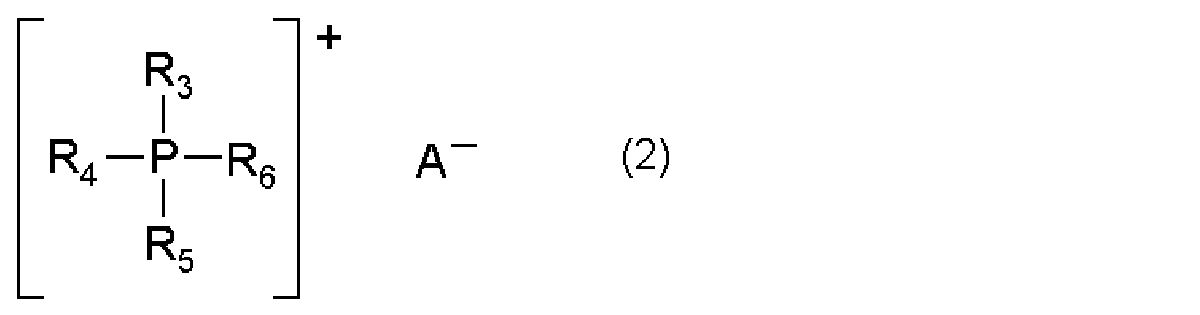
(カップリング剤)
カップリング剤1:エポキシシラン(信越化学工業社製、KBM-403)
(レベリング剤)
レベリング剤1:レベリング剤(ビックケミージャパン社製、BYK-356)
(光反応開始剤)
光反応開始剤1:2,4,6-トリメチルベンゾイル-ジフェニル-フォスフィンオキサイド(BASFジャパン社製、TPO)
光反応開始剤2:2-ベンジル-2-ジメチルアミノ-1-(4-モルフォリノフェニル)-ブタノン-1(BASFジャパン社製、イルガキュア369)
光反応開始剤3:オキシム化合物(BASFジャパン社製、OXE-02)
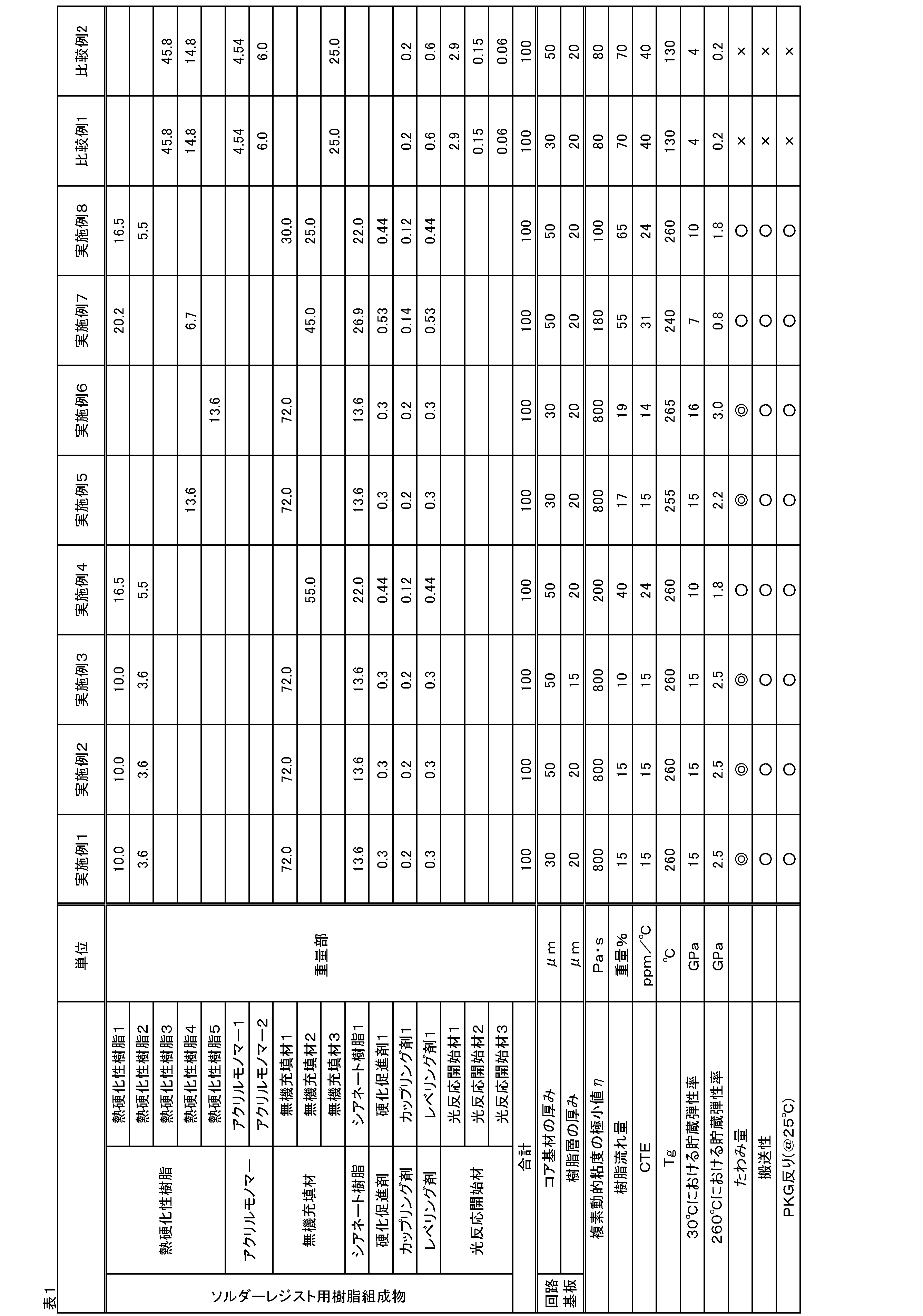
エポキシ樹脂として、ナフトール型エポキシ樹脂(日本化薬社製、NC-7000L)10.0重量部、2官能ナフタレン型エポキシ樹脂(DIC社製、HP-4032D)3.6重量部、ノボラックフェノール型シアネートエステル樹脂(ロンザジャパン社製、PT-30)13.6重量部、平均粒径D50が1μmの球状シリカ(アドマテックス社製、SC4050)固形分で72重量部、テトラフェニルホスホニウムのビス(ナフタレン-2,3-ジオキシ)フェニルシリケート付加物0.3重量部、エポキシシラン(信越化学工業社製、KBM-403)0.2重量部、およびレベリング剤(ビックケミージャパン社製、BYK-356)0.3重量部をメチルエチルケトンに溶解、分散させ、高速撹拌装置を用いて30分間撹拌して、不揮発分70重量%となるように調整し、樹脂組成物のワニス(樹脂ワニス)を調製した。
エポキシ樹脂として、ナフトール型エポキシ樹脂(日本化薬社製、NC-7000L)16.5重量部、2官能ナフタレン型エポキシ樹脂(DIC社製、HP-4032D)5.5重量部、ノボラックフェノール型シアネートエステル樹脂(ロンザジャパン社製、PT-30)22.0重量部、平均粒径D50が0.5μmの球状シリカ(アドマテックス社製、SC2050)固形分で55重量部、テトラフェニルホスホニウムのビス(ナフタレン-2,3-ジオキシ)フェニルシリケート付加物0.44重量部、エポキシシラン(信越化学工業社製、KBM-403)0.12重量部、およびレベリング剤(ビックケミージャパン社製、BYK-356)0.44重量部をメチルエチルケトンに溶解、分散させ、高速撹拌装置を用いて30分間撹拌して、不揮発分70重量%となるように調整し、樹脂組成物のワニス(樹脂ワニス)を調製した。
表1に記載の成分を用いて、実施例1と同様にして、樹脂組成物のワニス(樹脂ワニス)を調製した。
エポキシ樹脂として、ナフトール型エポキシ樹脂(日本化薬社製、NC-7000L)20.2重量部、ビフェニルジメチレン型エポキシ樹脂(日本化薬社製、NC-3000L)6.7重量部、ノボラックフェノール型シアネートエステル樹脂(ロンザジャパン社製、PT-30)26.9重量部、球状シリカ(アドマテックス社製、SC2050、平均粒径D50:0.5μm)固形分で45重量部、テトラフェニルホスホニウムのビス(ナフタレン-2,3-ジオキシ)フェニルシリケート付加物(住友ベークライト社製、C05-MB)0.53重量部、エポキシシラン(信越化学工業社製、KBM-403)0.14重量部、およびレベリング剤(ビックケミージャパン社製、BYK-356)0.53重量部をメチルエチルケトンに溶解、分散させ、高速撹拌装置を用いて30分間撹拌して、不揮発分70重量%となるように調整し、樹脂組成物のワニス(樹脂ワニス)を調製した。
エポキシ樹脂として、ナフトール型エポキシ樹脂(日本化薬社製、NC-7000L)16.5重量部、2官能ナフタレン型エポキシ樹脂(DIC社製、HP-4032D)5.5重量部、ノボラックフェノール型シアネートエステル樹脂(ロンザジャパン社製、PT-30)22重量部、球状シリカ(アドマテックス社製、SC4050、平均粒径D50:1μm)固形分で30重量部、球状シリカ(アドマテックス社製、SC2050、平均粒径D50:0.5μm)固形分で25重量部、テトラフェニルホスホニウムのビス(ナフタレン-2,3-ジオキシ)フェニルシリケート付加物(住友ベークライト社製、C05-MB)0.44重量部、エポキシシラン(信越化学工業社製、KBM-403)0.12重量部、およびレベリング剤(ビックケミージャパン社製、BYK-356)0.44重量部をメチルエチルケトンに溶解、分散させ、高速撹拌装置を用いて30分間撹拌して、不揮発分70重量%となるように調整し、ワニス状の樹脂組成物(樹脂ワニス)を調製した。
エポキシアクリレート樹脂(日本化薬社製、ZFR-1401)45.8重量部、エポキシ樹脂としてビフェニルジメチレン型エポキシ樹脂(日本化薬社製、NC-3000L)14.8重量部、光反応開始剤として、2,4,6-トリメチルベンゾイル-ジフェニル-フォスフィンオキサイド(BASFジャパン社製、TPO)2.9重量部、2-ベンジル-2-ジメチルアミノ-1-(4-モルフォリノフェニル)-ブタノン-1(BASFジャパン社製、イルガキュア369)0.15重量部、オキシム化合物(BASFジャパン社製、OXE-02)0.06重量部、2官能エトキシ化ビスフェノールAジメタクリレート(新中村化学社製、BPE-500)4.54重量部、2官能のウレタンアクリレート(日本化薬(株社製、KAYARAD UX-2201)6.0重量部、エポキシシラン(信越化学工業社製、KBM-403)0.15重量部、およびレベリング剤(ビックケミージャパン社製、BYK-356)0.6重量部をジプロピレングリコールモノメチルエーテルに溶解、分散させた。次いで、平均粒径D50が0.3μmの球状シリカ(アドマテックス社製、SC1050)固形分で25重量部を加え、高速撹拌装置を用いて30分間撹拌し不揮発分70重量%となるように調整し、樹脂組成物のワニス(樹脂ワニス)を調製した。
各実施例および各比較例について、得られた樹脂組成物のワニス(樹脂ワニス)をキャリア基材であるPETフィルム上に塗布した後、140℃、2分の条件で溶剤を除去して、所定の樹脂厚みを有する樹脂層を形成した。これにより、樹脂シートを得た。
各実施例および各比較例について、次のようにして最低複素動的粘度(複素度粘度の極小値)を測定した。まず、上記樹脂シートの作製に基づいて、20μmの樹脂厚みを有する樹脂層が形成された樹脂シートを得た。次いで、得られた樹脂シートから、キャリア基材であるPETフィルムを剥離した樹脂層(フィルム)を5枚重ね合わせて、総膜厚100μmの測定サンプルを準備した。次いで、この測定サンプルに対し、動的粘弾性測定装置(Anton Paar社製、装置名Physica MCR-301)を用いて、下記の条件で複素動的粘度の測定をおこなった。得られた測定結果から、50~150℃における最低複素動的粘度(Pa・sec)を算出した。
周波数:62.83rad/sec
測定温度:50~200℃
昇温速度:3℃/min
ジオメトリー:パラレルプレート
プレート直径:10mm
荷重(ノーマルフォース):0N(一定)
ストレイン:0.3%
測定雰囲気:空気
各実施例および各比較例について、上記樹脂シートの作製に基づいて、20μmの樹脂厚みを有する樹脂層が形成された樹脂シートを得た。次いで、得られた樹脂シートから、キャリア基材であるPETフィルムを剥離した樹脂層(フィルム)を5枚重ね合わせて、総膜厚100μmの積層フィルムを準備した。次いで、当該積層フィルムを、200℃、1時間で熱処理した後、幅8mm×長さ50mm×厚さ100μmに切り出して測定サンプルとした。この測定サンプルに対し、動的粘弾性測定装置(セイコーインスツルメンツ社製、DMS6100)を用いて、周波数1Hz、昇温速度5℃/分の条件で動的粘弾性試験を行った。次いで、得られた測定結果から、ガラス転移温度(℃)と、30℃における貯蔵弾性率(GPa)、260℃における貯蔵弾性率(GPa)を算出した。ガラス転移温度は、tanδのピーク値から判定した。結果を表1に示す。
各実施例および各比較例について、上記樹脂シートの作製に基づいて、20μmの樹脂厚みを有する樹脂層が形成された樹脂シートを得た。次いで、得られた樹脂シートから、キャリア基材であるPETフィルムを剥離した樹脂層(フィルム)を5枚重ね合わせて、総膜厚100μmの積層フィルムを準備した。次いで、当該積層フィルムを、200℃、1時間で熱処理した後、幅4mm×長さ20mm×厚さ100μmに切り出して測定サンプルとした。この測定サンプルに対し、TMA(TAインスツルメンツ(株)製)を用いて、昇温速度10℃/分の条件で線膨張係数の測定を行った。次いで、50~75℃における測定結果の平均を算出し、これをガラス転移温度未満における線膨張係数(ppm/℃)とした。結果を表1に示す。
・サンプルサイズ113mmφで基材ごと打ち抜く
・基材つきのまま4枚重ね(W0)
・温度171±3℃、圧力750±50kPaの条件で加熱加圧
・113mmφからはみ出した樹脂を除いた重量を測定(W1)
(W0-W1)/(W0-基材重量)×100
各実施例および各比較例について、得られた樹脂組成物をキャリア基材に塗布した後、140℃、2分の条件で溶剤を除去して、表1に示す膜厚の樹脂層を形成した。コア基材(LAZ-4785TH-G、住友ベークライト社製、50mm×85mm、表1に示す膜厚)の一面および他面上に12μm厚の銅箔を積層してなる両面銅張積層板を準備した。次いで、上記両面銅張積層板の銅箔をエッチング処理して銅箔を除去した基板を得た。次いで、上記基板の上記一面上および上記他面上のそれぞれに、前記樹脂層が上記基板と対向するように、当該樹脂シートを積層した後、真空加圧式ラミネーター装置を用いて温度120℃、圧力0.8MPa、120秒の条件にて真空加熱加圧成形した。次いで、当該樹脂シートから前記キャリア基材を剥離した後、上記基板上の前記樹脂層を200℃、1時間の条件で硬化してソルダーレジストを形成した。このようにして、サンプルを得た。得られたサンプルについて、短辺である一辺の端から10mmを支持しつつ上記一辺に対向する他辺を自由端とした状態において、上記他辺のたわみ量を測定した。
たわみ量の判定基準:
◎:15mm以下
○:15mmより大きい、かつ35mmより小さい
×:35mm以下
各実施例および各比較例について、得られた樹脂組成物をキャリア基材に塗布した後、140℃、2分の条件で溶剤を除去して、表1に示す膜厚の樹脂層を形成した。コア基材(LAZ-4785TH-G、住友ベークライト社製、250mm×250mm、表1に示す膜厚)の一面および他面上に12μm厚の銅箔を積層してなる両面銅張積層板を準備した。次いで、上記両面銅張積層板の銅箔をエッチング処理して銅箔を除去した基板を得た。次いで、上記基板の上記一面上および上記他面上のそれぞれに、前記樹脂層が上記基板と対向するように、当該樹脂シートを積層した後、真空加圧式ラミネーター装置を用いて温度120℃、圧力0.8MPa、120秒の条件にて真空加熱加圧成形する。次いで、当該樹脂シートから前記キャリア基材を剥離した後、上記基板上の前記樹脂層を200℃、1時間の条件で硬化してソルダーレジストを形成した。このようにして、サンプルを得る。得られたサンプルについて、フィルム搬送加圧式真空ラミネータ(名機製作所社製、MVLP500/600)で搬送性を評価した。評価方法は、搬送開始時の基板のセット位置から、1次加圧として真空30秒後0.5MPaで30秒後、2加圧として0.8MPaで60秒後の基板4つの角の位置ズレ量の最大値を測定した。
搬送性の判定基準:
○:15mm以下
×:15mmより大きい
各実施例および各比較例について、次のようにして半導体パッケージを作製した。まず、30μm厚のコア基材(LAZ-4785TH-G、住友ベークライト社製)の一面および他面上に12μm厚の銅箔を積層してなる両面銅張積層板を準備した。次いで、上記銅張積層板の銅箔をエッチング処理して導体回路パターンを形成することにより、一面および他面に上記導体回路パターンが形成された回路基板を得た。次いで、回路基板の上記一面上および上記他面上のそれぞれに、樹脂層が回路基板と対向するように、上記で得られた表1に示す膜厚の樹脂シートを積層した後、真空加圧式ラミネーター装置を用いて温度120℃、圧力0.8MPa、60秒の条件にて真空加熱加圧成形させた。次いで、樹脂シートからキャリア基材であるPETフィルムを剥離した後、回路基板上の樹脂層を200℃、1時間の条件で硬化してソルダーレジストを形成した。
各実施例および各比較例について、得られた半導体パッケージの25℃における反り量を測定した。このとき、パッケージ反り量が150μm未満であるものを○とし、パッケージ反り量が150μm以上であるものを×として、パッケージ反りを評価した。なお、パッケージ反り量は、半導体パッケージ上面の中心点と、当該上面の外周部と、の半導体素子と回路基板の積層方向における距離により定義される。
Claims (11)
- キャリア基材と、
前記キャリア基材上に配置されていて、ソルダーレジスト用樹脂組成物からなる樹脂層と、を備える、ソルダーレジストに用いる樹脂シートであって、
前記樹脂層の膜厚が、1μm以上50μm以下であり、
前記樹脂層のBステージ状態の動的粘弾性試験による、測定範囲50~200℃、昇温速度3℃/min、周波数62.83rad/secでの複素動的粘度の極小値をηとしたとき、ηが、100Pa・s以上3000Pa・s以下であり、
前記樹脂層の硬化物の30℃における貯蔵弾性率が7GPa以上40GPa以下である、樹脂シート。 - 請求項1に記載の樹脂シートであって、
前記樹脂層の硬化物のガラス転移温度が、160℃以上である、樹脂シート。 - 請求項1または2に記載の樹脂シートであって、
前記樹脂層の硬化物のガラス転移温度未満における線膨張係数が1ppm/℃以上35ppm/℃以下である、樹脂シート。 - 請求項1から3のいずれか1項に記載の樹脂シートであって、
前記樹脂層の硬化物の260℃における貯蔵弾性率が0.2GPa以上10GPa以下である、樹脂シート。 - 請求項1から4のいずれか1項に記載の樹脂シートであって、
下記条件で測定した前記樹脂層のBステージ状態の樹脂流れ量が、5重量%以上70重量%未満である、樹脂シート。
(樹脂流れ量の測定条件)
・サンプルサイズ113mmφで基材ごと打ち抜く
・基材つきのまま4枚重ね(W0)
・温度171±3℃、圧力750±50kPaの条件で加熱加圧
・113mmφからはみ出した樹脂を除いた重量を測定(W1)
(W0-W1)/(W0-基材重量)×100 - 請求項1から5のいずれか1項に記載の樹脂シートであって、
ガラス繊維基材を有しない基板の表面に形成されるソルダーレジストに用いる、樹脂シート。 - 請求項1から6のいずれか1項に記載の樹脂シートであって、
前記ソルダーレジスト用樹脂組成物が、熱硬化性樹脂と充填材とを含む、樹脂シート。 - 請求項7に記載の樹脂シートであって、
前記熱硬化性樹脂が、エポキシ樹脂を含む、樹脂シート。 - 請求項7または8に記載の樹脂シートであって、
前記充填材が、シリカを含む、樹脂シート。 - 請求項7から9のいずれか1項に記載の樹脂シートであって、
前記ソルダーレジスト用樹脂組成物が、シアネート樹脂をさらに含む、樹脂シート。 - 請求項1から10のいずれか1項に記載の樹脂シートであって、
下記の条件で測定されるたわみ量が35mm未満である、樹脂シート。
(たわみ量の測定条件)
ソルダーレジスト用樹脂組成物をキャリア基材に塗布した後、140℃、2分の条件で溶剤を除去して、厚さ20μmの樹脂層を形成する。コア基材(50mm×85mm、30μmt)の一面および他面上に12μm厚の銅箔を積層してなる両面銅張積層板を準備する。次いで、上記両面銅張積層板の銅箔をエッチング処理して銅箔を除去した基板を得る。次いで、上記基板の一面および他面上のそれぞれに、上記樹脂層が上記基板と対向するように、当該樹脂シートを積層した後、真空加圧式ラミネーター装置を用いて温度120℃、圧力0.8MPa、120秒の条件にて真空加熱加圧成形する。次いで、当該樹脂シートから上記キャリア基材を剥離した後、上記基板上の上記樹脂層を200℃、1時間の条件で硬化してソルダーレジストを形成した。このようにして、サンプルを得る。得られたサンプルについて、短辺である一辺の端から10mmを支持しつつ上記一辺に対向する他辺を自由端とした状態において、上記他辺のたわみ量を測定する。
Priority Applications (1)
| Application Number | Priority Date | Filing Date | Title |
|---|---|---|---|
| KR1020187024273A KR101991378B1 (ko) | 2016-03-02 | 2017-02-20 | 수지 시트 |
Applications Claiming Priority (2)
| Application Number | Priority Date | Filing Date | Title |
|---|---|---|---|
| JP2016040405A JP6107992B1 (ja) | 2016-03-02 | 2016-03-02 | 樹脂シート |
| JP2016-040405 | 2016-03-02 |
Publications (1)
| Publication Number | Publication Date |
|---|---|
| WO2017150231A1 true WO2017150231A1 (ja) | 2017-09-08 |
Family
ID=58666438
Family Applications (1)
| Application Number | Title | Priority Date | Filing Date |
|---|---|---|---|
| PCT/JP2017/006047 Ceased WO2017150231A1 (ja) | 2016-03-02 | 2017-02-20 | 樹脂シート |
Country Status (4)
| Country | Link |
|---|---|
| JP (1) | JP6107992B1 (ja) |
| KR (1) | KR101991378B1 (ja) |
| TW (1) | TWI633141B (ja) |
| WO (1) | WO2017150231A1 (ja) |
Cited By (1)
| Publication number | Priority date | Publication date | Assignee | Title |
|---|---|---|---|---|
| WO2019068461A1 (de) * | 2017-10-06 | 2019-04-11 | Conti Temic Microelectronic Gmbh | Verfahren zum herstellen einer elektronischen komponente, elektronische komponente und lötstopplack |
Families Citing this family (2)
| Publication number | Priority date | Publication date | Assignee | Title |
|---|---|---|---|---|
| WO2021261179A1 (ja) | 2020-06-26 | 2021-12-30 | 住友ベークライト株式会社 | 回路基板 |
| CN117915562A (zh) * | 2022-10-19 | 2024-04-19 | 鹏鼎控股(深圳)股份有限公司 | 电路板及其制作方法 |
Citations (4)
| Publication number | Priority date | Publication date | Assignee | Title |
|---|---|---|---|---|
| JP2004311527A (ja) * | 2003-04-02 | 2004-11-04 | Ngk Spark Plug Co Ltd | 配線基板、並びに配線基板の製造方法 |
| JP2006278993A (ja) * | 2005-03-30 | 2006-10-12 | Sumitomo Bakelite Co Ltd | 配線板 |
| JP2012073600A (ja) * | 2010-08-31 | 2012-04-12 | Fujifilm Corp | 感光性組成物、並びに、感光性フィルム、永久パターン、永久パターン形成方法、及びプリント基板 |
| JP2012136693A (ja) * | 2010-12-08 | 2012-07-19 | Ajinomoto Co Inc | 樹脂組成物 |
Family Cites Families (5)
| Publication number | Priority date | Publication date | Assignee | Title |
|---|---|---|---|---|
| JP2002064252A (ja) * | 2000-08-22 | 2002-02-28 | Kanegafuchi Chem Ind Co Ltd | ポリイミドフィルム、及びこれを用いた積層体、多層配線板 |
| JP5056787B2 (ja) * | 2009-03-31 | 2012-10-24 | 住友ベークライト株式会社 | 積層板、多層プリント配線板および半導体装置 |
| WO2012176423A1 (ja) * | 2011-06-21 | 2012-12-27 | 住友ベークライト株式会社 | 積層板の製造方法 |
| JP5564144B1 (ja) | 2013-01-15 | 2014-07-30 | 太陽インキ製造株式会社 | 硬化性樹脂組成物、そのドライフィルム及び硬化物並びにそれらを用いたプリント配線板 |
| WO2015072261A1 (ja) * | 2013-11-12 | 2015-05-21 | 住友ベークライト株式会社 | 樹脂層付きキャリア材料、積層体、回路基板および電子装置 |
-
2016
- 2016-03-02 JP JP2016040405A patent/JP6107992B1/ja active Active
-
2017
- 2017-02-20 WO PCT/JP2017/006047 patent/WO2017150231A1/ja not_active Ceased
- 2017-02-20 KR KR1020187024273A patent/KR101991378B1/ko active Active
- 2017-02-23 TW TW106106034A patent/TWI633141B/zh active
Patent Citations (4)
| Publication number | Priority date | Publication date | Assignee | Title |
|---|---|---|---|---|
| JP2004311527A (ja) * | 2003-04-02 | 2004-11-04 | Ngk Spark Plug Co Ltd | 配線基板、並びに配線基板の製造方法 |
| JP2006278993A (ja) * | 2005-03-30 | 2006-10-12 | Sumitomo Bakelite Co Ltd | 配線板 |
| JP2012073600A (ja) * | 2010-08-31 | 2012-04-12 | Fujifilm Corp | 感光性組成物、並びに、感光性フィルム、永久パターン、永久パターン形成方法、及びプリント基板 |
| JP2012136693A (ja) * | 2010-12-08 | 2012-07-19 | Ajinomoto Co Inc | 樹脂組成物 |
Cited By (1)
| Publication number | Priority date | Publication date | Assignee | Title |
|---|---|---|---|---|
| WO2019068461A1 (de) * | 2017-10-06 | 2019-04-11 | Conti Temic Microelectronic Gmbh | Verfahren zum herstellen einer elektronischen komponente, elektronische komponente und lötstopplack |
Also Published As
| Publication number | Publication date |
|---|---|
| JP2017157722A (ja) | 2017-09-07 |
| KR101991378B1 (ko) | 2019-06-20 |
| TWI633141B (zh) | 2018-08-21 |
| TW201803937A (zh) | 2018-02-01 |
| JP6107992B1 (ja) | 2017-04-05 |
| KR20180099901A (ko) | 2018-09-05 |
Similar Documents
| Publication | Publication Date | Title |
|---|---|---|
| JP7119290B2 (ja) | 熱硬化性樹脂組成物、キャリア付樹脂膜、プリプレグ、プリント配線基板および半導体装置 | |
| TWI494337B (zh) | 電路基板用環氧樹脂組成物,預浸體,積層板,樹脂片,印刷佈線板用積層基材,印刷佈線板及半導體裝置 | |
| JP7258453B2 (ja) | 熱硬化性樹脂組成物、キャリア付樹脂膜、プリプレグ、プリント配線基板および半導体装置 | |
| KR102582537B1 (ko) | 프린트 배선판의 제조 방법, 반도체 장치의 제조 방법 | |
| KR101564179B1 (ko) | 도체 회로를 갖는 구조체 및 그 제조 방법 및 열경화성 수지 조성물 | |
| JP2014056924A (ja) | 半導体装置の製造方法及びそれに用いる熱硬化性樹脂組成物並びにそれらにより得られる半導体装置 | |
| JP6107992B1 (ja) | 樹脂シート | |
| JP6610069B2 (ja) | ソルダーレジスト用樹脂組成物、キャリア付樹脂膜、配線基板、電子装置、および電子装置の製造方法 | |
| JP2023126287A (ja) | ソルダーレジスト樹脂組成物、樹脂シート、梱包体及び回路基板 | |
| JP6641817B2 (ja) | 熱硬化性樹脂組成物、キャリア付樹脂膜、および半導体装置 | |
| JP6409390B2 (ja) | 配線基板、半導体パッケージ、電子装置、配線基板の製造方法、および半導体パッケージの製造方法 | |
| WO2018088345A1 (ja) | 金属箔付き樹脂膜、構造体、配線基板の製造方法、半導体装置の製造方法 | |
| KR102927866B1 (ko) | 회로 기판의 제조 방법 | |
| TW202342571A (zh) | 硬化性組成物 | |
| JP7225553B2 (ja) | ソルダーレジスト形成用の樹脂シート | |
| JP6739893B2 (ja) | 半導体封止用部材、半導体装置の製造方法及び半導体装置 | |
| JP2019091737A (ja) | 熱硬化性樹脂組成物、回路基板、及び、回路基板の製造方法 | |
| JP2017212400A (ja) | 樹脂シートおよび回路基板 | |
| JP7058467B2 (ja) | 樹脂シートおよび回路基板 | |
| TW201726404A (zh) | 構造體、佈線基板及佈線基板之製造方法 | |
| JP2017010992A (ja) | 半導体装置及びその製造方法 | |
| JP7240085B2 (ja) | 熱硬化性樹脂組成物、キャリア付樹脂膜、プリプレグ、プリント配線基板および半導体装置 | |
| JP2017048392A (ja) | 樹脂シート、および電子装置 | |
| JP2019095719A (ja) | 配線基板の製造方法、半導体装置の製造方法 | |
| JP6413437B2 (ja) | 配線基板の製造方法、および半導体パッケージの製造方法 |
Legal Events
| Date | Code | Title | Description |
|---|---|---|---|
| ENP | Entry into the national phase |
Ref document number: 20187024273 Country of ref document: KR Kind code of ref document: A |
|
| WWE | Wipo information: entry into national phase |
Ref document number: 1020187024273 Country of ref document: KR |
|
| NENP | Non-entry into the national phase |
Ref country code: DE |
|
| 121 | Ep: the epo has been informed by wipo that ep was designated in this application |
Ref document number: 17759699 Country of ref document: EP Kind code of ref document: A1 |
|
| 122 | Ep: pct application non-entry in european phase |
Ref document number: 17759699 Country of ref document: EP Kind code of ref document: A1 |