WO2017094780A1 - インドロカルバゾールノボラック樹脂を含むレジスト下層膜形成組成物 - Google Patents
インドロカルバゾールノボラック樹脂を含むレジスト下層膜形成組成物 Download PDFInfo
- Publication number
- WO2017094780A1 WO2017094780A1 PCT/JP2016/085561 JP2016085561W WO2017094780A1 WO 2017094780 A1 WO2017094780 A1 WO 2017094780A1 JP 2016085561 W JP2016085561 W JP 2016085561W WO 2017094780 A1 WO2017094780 A1 WO 2017094780A1
- Authority
- WO
- WIPO (PCT)
- Prior art keywords
- underlayer film
- group
- resist underlayer
- resist
- formula
- Prior art date
- Legal status (The legal status is an assumption and is not a legal conclusion. Google has not performed a legal analysis and makes no representation as to the accuracy of the status listed.)
- Ceased
Links
- 0 C*[n]1c2c(-c3ccccc3)c(-c3ccccc3)c(c3ccccc3[n]3*)c3c2c2ccccc12 Chemical compound C*[n]1c2c(-c3ccccc3)c(-c3ccccc3)c(c3ccccc3[n]3*)c3c2c2ccccc12 0.000 description 5
- ABXYEXYYZFXNKO-UHFFFAOYSA-N CCC(C)c1c(cccc2)c2cc2c1cccc2 Chemical compound CCC(C)c1c(cccc2)c2cc2c1cccc2 ABXYEXYYZFXNKO-UHFFFAOYSA-N 0.000 description 1
Classifications
-
- G—PHYSICS
- G03—PHOTOGRAPHY; CINEMATOGRAPHY; ANALOGOUS TECHNIQUES USING WAVES OTHER THAN OPTICAL WAVES; ELECTROGRAPHY; HOLOGRAPHY
- G03F—PHOTOMECHANICAL PRODUCTION OF TEXTURED OR PATTERNED SURFACES, e.g. FOR PRINTING, FOR PROCESSING OF SEMICONDUCTOR DEVICES; MATERIALS THEREFOR; ORIGINALS THEREFOR; APPARATUS SPECIALLY ADAPTED THEREFOR
- G03F7/00—Photomechanical, e.g. photolithographic, production of textured or patterned surfaces, e.g. printing surfaces; Materials therefor, e.g. comprising photoresists; Apparatus specially adapted therefor
- G03F7/004—Photosensitive materials
- G03F7/09—Photosensitive materials characterised by structural details, e.g. supports, auxiliary layers
- G03F7/11—Photosensitive materials characterised by structural details, e.g. supports, auxiliary layers having cover layers or intermediate layers, e.g. subbing layers
-
- C—CHEMISTRY; METALLURGY
- C08—ORGANIC MACROMOLECULAR COMPOUNDS; THEIR PREPARATION OR CHEMICAL WORKING-UP; COMPOSITIONS BASED THEREON
- C08G—MACROMOLECULAR COMPOUNDS OBTAINED OTHERWISE THAN BY REACTIONS ONLY INVOLVING UNSATURATED CARBON-TO-CARBON BONDS
- C08G12/00—Condensation polymers of aldehydes or ketones with only compounds containing hydrogen attached to nitrogen
- C08G12/02—Condensation polymers of aldehydes or ketones with only compounds containing hydrogen attached to nitrogen of aldehydes
- C08G12/26—Condensation polymers of aldehydes or ketones with only compounds containing hydrogen attached to nitrogen of aldehydes with heterocyclic compounds
-
- C—CHEMISTRY; METALLURGY
- C08—ORGANIC MACROMOLECULAR COMPOUNDS; THEIR PREPARATION OR CHEMICAL WORKING-UP; COMPOSITIONS BASED THEREON
- C08G—MACROMOLECULAR COMPOUNDS OBTAINED OTHERWISE THAN BY REACTIONS ONLY INVOLVING UNSATURATED CARBON-TO-CARBON BONDS
- C08G16/00—Condensation polymers of aldehydes or ketones with monomers not provided for in the groups C08G4/00 - C08G14/00
- C08G16/02—Condensation polymers of aldehydes or ketones with monomers not provided for in the groups C08G4/00 - C08G14/00 of aldehydes
-
- C—CHEMISTRY; METALLURGY
- C08—ORGANIC MACROMOLECULAR COMPOUNDS; THEIR PREPARATION OR CHEMICAL WORKING-UP; COMPOSITIONS BASED THEREON
- C08G—MACROMOLECULAR COMPOUNDS OBTAINED OTHERWISE THAN BY REACTIONS ONLY INVOLVING UNSATURATED CARBON-TO-CARBON BONDS
- C08G16/00—Condensation polymers of aldehydes or ketones with monomers not provided for in the groups C08G4/00 - C08G14/00
- C08G16/02—Condensation polymers of aldehydes or ketones with monomers not provided for in the groups C08G4/00 - C08G14/00 of aldehydes
- C08G16/025—Condensation polymers of aldehydes or ketones with monomers not provided for in the groups C08G4/00 - C08G14/00 of aldehydes with heterocyclic organic compounds
- C08G16/0268—Condensation polymers of aldehydes or ketones with monomers not provided for in the groups C08G4/00 - C08G14/00 of aldehydes with heterocyclic organic compounds containing nitrogen in the ring
-
- C—CHEMISTRY; METALLURGY
- C09—DYES; PAINTS; POLISHES; NATURAL RESINS; ADHESIVES; COMPOSITIONS NOT OTHERWISE PROVIDED FOR; APPLICATIONS OF MATERIALS NOT OTHERWISE PROVIDED FOR
- C09D—COATING COMPOSITIONS, e.g. PAINTS, VARNISHES OR LACQUERS; FILLING PASTES; CHEMICAL PAINT OR INK REMOVERS; INKS; CORRECTING FLUIDS; WOODSTAINS; PASTES OR SOLIDS FOR COLOURING OR PRINTING; USE OF MATERIALS THEREFOR
- C09D161/00—Coating compositions based on condensation polymers of aldehydes or ketones; Coating compositions based on derivatives of such polymers
- C09D161/20—Condensation polymers of aldehydes or ketones with only compounds containing hydrogen attached to nitrogen
- C09D161/26—Condensation polymers of aldehydes or ketones with only compounds containing hydrogen attached to nitrogen of aldehydes with heterocyclic compounds
-
- G—PHYSICS
- G03—PHOTOGRAPHY; CINEMATOGRAPHY; ANALOGOUS TECHNIQUES USING WAVES OTHER THAN OPTICAL WAVES; ELECTROGRAPHY; HOLOGRAPHY
- G03F—PHOTOMECHANICAL PRODUCTION OF TEXTURED OR PATTERNED SURFACES, e.g. FOR PRINTING, FOR PROCESSING OF SEMICONDUCTOR DEVICES; MATERIALS THEREFOR; ORIGINALS THEREFOR; APPARATUS SPECIALLY ADAPTED THEREFOR
- G03F7/00—Photomechanical, e.g. photolithographic, production of textured or patterned surfaces, e.g. printing surfaces; Materials therefor, e.g. comprising photoresists; Apparatus specially adapted therefor
- G03F7/20—Exposure; Apparatus therefor
-
- G—PHYSICS
- G03—PHOTOGRAPHY; CINEMATOGRAPHY; ANALOGOUS TECHNIQUES USING WAVES OTHER THAN OPTICAL WAVES; ELECTROGRAPHY; HOLOGRAPHY
- G03F—PHOTOMECHANICAL PRODUCTION OF TEXTURED OR PATTERNED SURFACES, e.g. FOR PRINTING, FOR PROCESSING OF SEMICONDUCTOR DEVICES; MATERIALS THEREFOR; ORIGINALS THEREFOR; APPARATUS SPECIALLY ADAPTED THEREFOR
- G03F7/00—Photomechanical, e.g. photolithographic, production of textured or patterned surfaces, e.g. printing surfaces; Materials therefor, e.g. comprising photoresists; Apparatus specially adapted therefor
- G03F7/20—Exposure; Apparatus therefor
- G03F7/2002—Exposure; Apparatus therefor with visible light or UV light, through an original having an opaque pattern on a transparent support, e.g. film printing, projection printing; by reflection of visible or UV light from an original such as a printed image
-
- G—PHYSICS
- G03—PHOTOGRAPHY; CINEMATOGRAPHY; ANALOGOUS TECHNIQUES USING WAVES OTHER THAN OPTICAL WAVES; ELECTROGRAPHY; HOLOGRAPHY
- G03F—PHOTOMECHANICAL PRODUCTION OF TEXTURED OR PATTERNED SURFACES, e.g. FOR PRINTING, FOR PROCESSING OF SEMICONDUCTOR DEVICES; MATERIALS THEREFOR; ORIGINALS THEREFOR; APPARATUS SPECIALLY ADAPTED THEREFOR
- G03F7/00—Photomechanical, e.g. photolithographic, production of textured or patterned surfaces, e.g. printing surfaces; Materials therefor, e.g. comprising photoresists; Apparatus specially adapted therefor
- G03F7/20—Exposure; Apparatus therefor
- G03F7/2051—Exposure without an original mask, e.g. using a programmed deflection of a point source, by scanning, by drawing with a light beam, using an addressed light or corpuscular source
- G03F7/2059—Exposure without an original mask, e.g. using a programmed deflection of a point source, by scanning, by drawing with a light beam, using an addressed light or corpuscular source using a scanning corpuscular radiation beam, e.g. an electron beam
-
- G—PHYSICS
- G03—PHOTOGRAPHY; CINEMATOGRAPHY; ANALOGOUS TECHNIQUES USING WAVES OTHER THAN OPTICAL WAVES; ELECTROGRAPHY; HOLOGRAPHY
- G03F—PHOTOMECHANICAL PRODUCTION OF TEXTURED OR PATTERNED SURFACES, e.g. FOR PRINTING, FOR PROCESSING OF SEMICONDUCTOR DEVICES; MATERIALS THEREFOR; ORIGINALS THEREFOR; APPARATUS SPECIALLY ADAPTED THEREFOR
- G03F7/00—Photomechanical, e.g. photolithographic, production of textured or patterned surfaces, e.g. printing surfaces; Materials therefor, e.g. comprising photoresists; Apparatus specially adapted therefor
- G03F7/26—Processing photosensitive materials; Apparatus therefor
-
- G—PHYSICS
- G03—PHOTOGRAPHY; CINEMATOGRAPHY; ANALOGOUS TECHNIQUES USING WAVES OTHER THAN OPTICAL WAVES; ELECTROGRAPHY; HOLOGRAPHY
- G03F—PHOTOMECHANICAL PRODUCTION OF TEXTURED OR PATTERNED SURFACES, e.g. FOR PRINTING, FOR PROCESSING OF SEMICONDUCTOR DEVICES; MATERIALS THEREFOR; ORIGINALS THEREFOR; APPARATUS SPECIALLY ADAPTED THEREFOR
- G03F7/00—Photomechanical, e.g. photolithographic, production of textured or patterned surfaces, e.g. printing surfaces; Materials therefor, e.g. comprising photoresists; Apparatus specially adapted therefor
- G03F7/26—Processing photosensitive materials; Apparatus therefor
- G03F7/40—Treatment after imagewise removal, e.g. baking
-
- H—ELECTRICITY
- H10—SEMICONDUCTOR DEVICES; ELECTRIC SOLID-STATE DEVICES NOT OTHERWISE PROVIDED FOR
- H10P—GENERIC PROCESSES OR APPARATUS FOR THE MANUFACTURE OR TREATMENT OF DEVICES COVERED BY CLASS H10
- H10P76/00—Manufacture or treatment of masks on semiconductor bodies, e.g. by lithography or photolithography
-
- H—ELECTRICITY
- H10—SEMICONDUCTOR DEVICES; ELECTRIC SOLID-STATE DEVICES NOT OTHERWISE PROVIDED FOR
- H10P—GENERIC PROCESSES OR APPARATUS FOR THE MANUFACTURE OR TREATMENT OF DEVICES COVERED BY CLASS H10
- H10P76/00—Manufacture or treatment of masks on semiconductor bodies, e.g. by lithography or photolithography
- H10P76/20—Manufacture or treatment of masks on semiconductor bodies, e.g. by lithography or photolithography of masks comprising organic materials
- H10P76/204—Manufacture or treatment of masks on semiconductor bodies, e.g. by lithography or photolithography of masks comprising organic materials of organic photoresist masks
- H10P76/2041—Photolithographic processes
Definitions
- the present invention relates to a resist underlayer film forming composition using an indolocarbazole novolak resin.
- polymers having a ring structure such as novolak have been widely used from fine fields such as photoresists to general fields such as automobiles and housing members. .
- a monomer having a ring structure includes structures such as benzene, naphthalene, anthracene, pyrene, and fluorene, and these monomers are known to form a novolak with a monomer having an aldehyde group.
- carbazole having a structure similar to that of fluorene has similar characteristics, and it has been revealed that both monomers are polymerized by reaction of a part of the benzene ring adjacent to the five-membered ring.
- a thin film of a photoresist composition is formed on a substrate to be processed such as a silicon wafer, and irradiated with actinic rays such as ultraviolet rays through a mask pattern on which a semiconductor device pattern is drawn, and developed.
- actinic rays such as ultraviolet rays
- This is a processing method for etching a substrate to be processed such as a silicon wafer using the obtained photoresist pattern as a protective film.
- Examples of polymers for the resist underlayer film include the following.
- Examples are resist underlayer film-forming compositions using carbazole (see Patent Document 1, Patent Document 2, Patent Document 3, and Patent Document 4).
- the present invention can also provide the ability to effectively absorb the reflected light from the substrate when the irradiation light is used for fine processing.
- this invention is providing the formation method of the resist pattern using the resist underlayer film forming composition.
- A is a divalent group having at least two amino groups, and the group has a condensed ring structure and an aromatic group that substitutes a hydrogen atom on the condensed ring.
- a resist underlayer film-forming composition comprising a polymer containing a unit structure represented by the following:
- the resist underlayer film forming composition according to the first aspect wherein A is a divalent group derived from a compound having an indolocarbazole structure in formula (1)
- the aromatic group that substitutes a hydrogen atom on the condensed ring of the compound having an indolocarbazole structure is a phenyl group
- A is Formula (2): (In formula (2), R 1 and R 2 each independently represents a hydrogen atom, an alkyl group having 1 to 10 carbon atoms, or an aryl
- the resist underlayer film forming composition according to the first aspect which is a divalent group
- the resist underlayer film forming composition according to the fourth aspect wherein the compound represented by the formula (2) is a reaction product obtained by reacting indole and benzyl in the presence of an acid compound.
- the resist underlayer film forming composition according to any one of the first aspect to the fifth aspect further including a crosslinking agent
- the resist underlayer film forming composition according to any one of the first aspect to the sixth aspect further comprising an acid and / or an acid generator
- a method for producing a resist underlayer film obtained by applying and baking the resist underlayer film forming composition according to any one of the first to seventh aspects on a semiconductor substrate As a ninth aspect, a step of forming a resist underlayer film from the resist underlayer film forming composition according to any one of the first to seventh aspects on a semiconductor substrate, a step of forming a resist film thereon, light Or a step of forming a resist pattern by electron beam irradiation and development, a step of etching the resist underlayer film with the formed resist pattern, and a step of processing a semiconductor substrate with the patterned resist underlayer film.
- B 1 and B 2 each independently represents a hydrogen atom, an alkyl group, a benzene ring group, a condensed ring group or a combination thereof, or B 1 and B 2 are carbons to which they are bonded. You may form a ring with an atom.
- the polymer which has a unit structure represented by these.
- the resist underlayer film forming composition for lithography of the present invention With the resist underlayer film forming composition for lithography of the present invention, a good resist pattern shape can be formed without causing intermixing between the upper layer portion of the resist underlayer film and the layer coated thereon.
- the resist underlayer film forming composition of the present invention can be imparted with the ability to efficiently suppress reflection from the substrate, and can also have an effect as an antireflection film for exposure light.
- the resist underlayer film forming composition of the present invention the dry etching rate selectivity close to the resist, the dry etching rate selectivity lower than that of the resist, and the dry etching rate selectivity lower than that of the semiconductor substrate are excellent.
- a resist underlayer film can be provided.
- the substrate has sufficient etching resistance against a processed substrate (for example, a thermal silicon oxide film, a silicon nitride film, a polysilicon film, etc. on the substrate). It is.
- a processed substrate for example, a thermal silicon oxide film, a silicon nitride film, a polysilicon film, etc. on the substrate.
- the resist is thinned.
- the resist pattern is transferred to the lower layer film by an etching process, the substrate processing is performed using the lower layer film as a mask, or the resist pattern is transferred to the lower layer film by an etching process, and further to the lower layer film.
- There is a process in which the process of transferring the transferred pattern to the lower layer film using a different gas composition is repeated to finally process the substrate.
- the resist underlayer film and the composition for forming the same of the present invention are effective for this process.
- the polymer used in the present invention is a polymer containing a unit structure having indolocarbazole, the heat resistance is extremely high.
- this hard mask formation is made of an inorganic substance (for example, silicon nitride oxide).
- the deposit is deposited on the resist underlayer film surface, and the temperature of the resist underlayer film surface rises to around 400 ° C. at that time. Since the resist underlayer film obtained by curing the resist underlayer film forming composition of the present invention has high heat resistance, thermal degradation does not occur even when deposits are deposited.
- the thermal stability is high as described above, and the generation of decomposition products (sublimation products) during firing can be reduced, so that contamination of the upper layer film can be prevented, Further, it is possible to provide a margin for the temperature margin of the firing process.
- the resist underlayer film of the present invention can be used as a planarizing film, a resist underlayer film, a resist layer antifouling film, and a film having dry etch selectivity. This makes it possible to easily and accurately form a resist pattern in a lithography process for manufacturing a semiconductor.
- the present invention relates to a polymer containing a unit structure represented by formula (1), and relates to a resist underlayer film forming composition containing a polymer containing a unit structure represented by formula (1).
- the said polymer and a solvent are included. And it can contain a crosslinking agent and an acid, and can contain additives, such as an acid generator and surfactant, as needed.
- the solid content of the composition is 0.1 to 70% by mass, or 0.1 to 60% by mass.
- the solid content is the content ratio of all components excluding the solvent from the resist underlayer film forming composition.
- the polymer can be contained in a solid content in a proportion of 1 to 100% by mass, or 1 to 99.9% by mass, or 50 to 99.9% by mass.
- the polymer used in the present invention has a weight average molecular weight of 600 to 1000000 or 600 to 200000.
- A is a divalent group having at least two amino groups, and the group has a condensed ring structure and an aromatic group that substitutes a hydrogen atom on the condensed ring.
- B 1 and B 2 each independently represent a hydrogen atom, an alkyl group, a benzene ring group, a condensed ring group or a combination thereof, or B 1 and B 2 are carbons to which they are bonded.
- a ring may be formed together with the atom.
- A is a divalent group having at least two secondary amino groups, and the group is derived from a compound having a condensed ring structure and an aromatic group that substitutes a hydrogen atom on the condensed ring. It is preferable to show a divalent group.
- A can represent a divalent group derived from a compound having an indolocarbazole structure.
- aromatic group that substitutes a hydrogen atom on the condensed ring having an indolocarbazole structure include a phenyl group, a naphthyl group, an anthryl group, and a pyrene group, and a phenyl group can be preferably used.
- a divalent group derived from the compound represented by formula (2) can be used.
- the polymer containing the unit structure represented by the formula (1) is a novel polymer, and is excellent as a component of the resist underlayer film forming composition of the present invention.
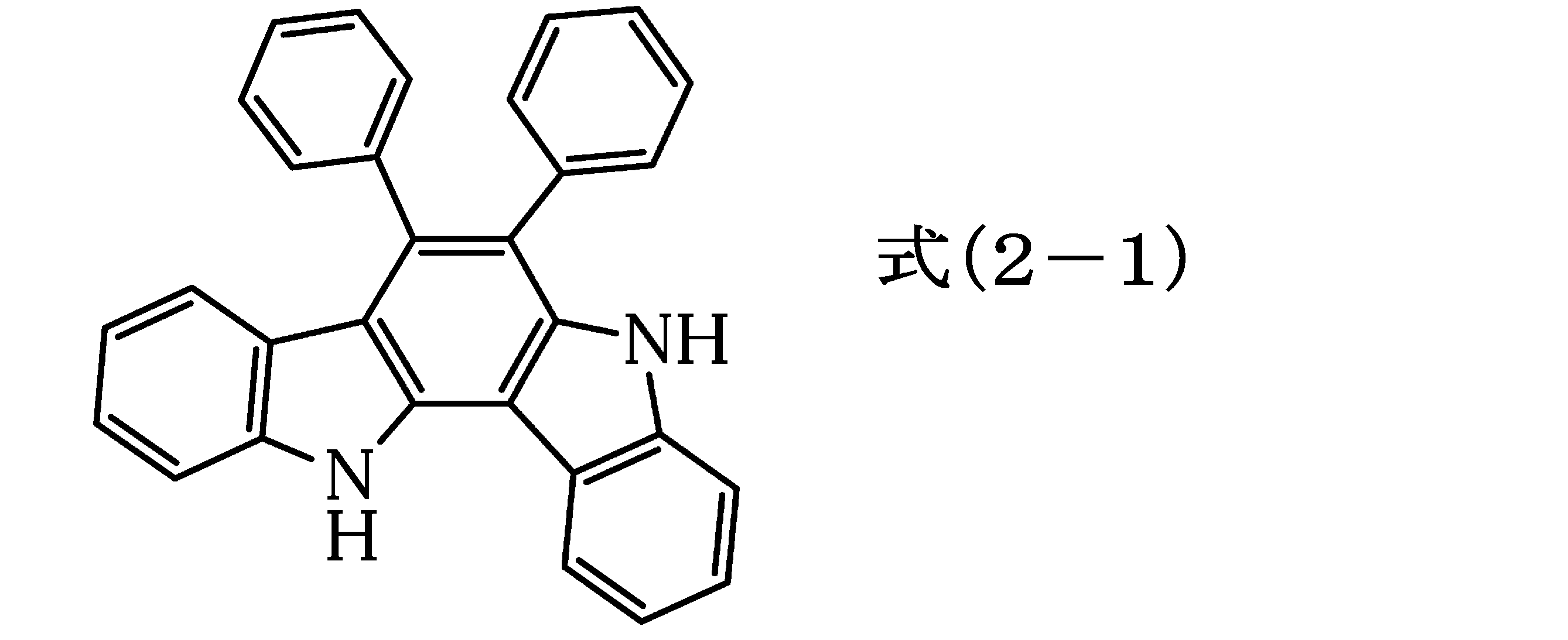
- the compound represented by the above formula (2) is diphenylindolocarbazole when R 1 and R 2 are hydrogen atoms, and derivatives thereof having a substituent for substituting a hydrogen atom on nitrogen. In the diphenylindolocarbazole, 1 mol of benzyl can be reacted with 2 mol of indole in the presence of an acid catalyst.
- organic sulfonic acids such as methanesulfonic acid, p-toluenesulfonic acid, and p-toluenesulfonic acid monohydrate can be preferably used. It can be synthesized by using a hydrocarbon solvent such as toluene and refluxing at a temperature of about 140 to 180 ° C. for 50 to 20 hours.
- R 1 and R 2 can each independently represent a hydrogen atom, an alkyl group having 1 to 10 carbon atoms, or an aryl group having 6 to 40 carbon atoms. In particular, a hydrogen atom can be used.
- alkyl group having 1 to 10 carbon atoms examples include methyl group, ethyl group, n-propyl group, i-propyl group, cyclopropyl group, n-butyl group, i-butyl group, s-butyl group, and t-butyl group.
- Cyclobutyl group 1-methyl-cyclopropyl group, 2-methyl-cyclopropyl group, n-pentyl group, 1-methyl-n-butyl group, 2-methyl-n-butyl group, 3-methyl-n-butyl Group, 1,1-dimethyl-n-propyl group, 1,2-dimethyl-n-propyl group, 2,2-dimethyl-n-propyl group, 1-ethyl-n-propyl group, cyclopentyl group, 1-methyl -Cyclobutyl group, 2-methyl-cyclobutyl group, 3-methyl-cyclobutyl group, 1,2-dimethyl-cyclopropyl group, 2,3-dimethyl-cyclopropyl group, 1-ethyl-cyclopropyl group 2-ethyl-cyclopropyl group, n-hexyl group, 1-methyl-n-pentyl group, 2-methyl-n-pentyl group, 3-methyl-n-pentyl group,
- aryl group having 6 to 40 carbon atoms examples include phenyl group, o-methylphenyl group, m-methylphenyl group, p-methylphenyl group, o-chlorophenyl group, m-chlorophenyl group, p-chlorophenyl group, o-fluorophenyl group, p-fluorophenyl group, o-methoxyphenyl group, p-methoxyphenyl group, p-nitrophenyl group, p-cyanophenyl group, ⁇ -naphthyl group, ⁇ -naphthyl group, o-biphenyl group M-biphenyl group, p-biphenyl group, 1-anthryl group, 2-anthryl group, 9-anthryl group, 1-phenanthryl group, 2-phenanthryl group, 3-phenanthryl group, 4-phenanthryl group, 9-phenanthryl group And a
- B 1 and B 2 in the unit structure represented by the formula (1) each independently represent a hydrogen atom, an alkyl group, a benzene ring group, a condensed ring group or a combination thereof, and B 1 and B 2 are bonded to each other. And may form a ring together with the carbon atoms.
- the combination means a group formed by a combination of an alkyl group and a benzene ring group or a condensed ring group, and examples thereof include a benzyl group and a methylanthracene group.
- B 1 and B 2 are groups derived from an aldehyde or a ketone having a hydrogen atom, an alkyl group, a benzene ring group, or a condensed ring group, which are raw materials for the production of a polymer having a unit structure represented by the formula (1).
- a novolac resin is formed with the compound providing a portion corresponding to A.
- the alkyl group is an alkyl group having 1 to 10 carbon atoms as described above.
- the condensed ring group is a condensed ring group corresponding to the above-mentioned aryl group having 10 to 40 carbon atoms, and examples thereof include a naphthyl group, an anthryl group, a pyrene group, and derivatives thereof.
- the aldehyde as a raw material for providing the group B 1 , B 2 portion includes formaldehyde when B 1 and B 2 are hydrogen atoms.
- B 1 is a hydrogen atom and B 2 is an alkyl group
- acetaldehyde, ethyl aldehyde, isobutyraldehyde and the like can be mentioned.
- B 1 is a hydrogen atom and B 2 is a benzene ring group
- benzaldehyde and the like can be mentioned.
- B 1 is a hydrogen atom and B 2 is a condensed ring group
- naphthyl aldehyde, anthryl aldehyde, pyrene carboxaldehyde and the like can be mentioned.
- B 1 is a hydrogen atom and B 2 is a combination of an alkyl group and a benzene ring, phenylacetaldehyde and the like can be mentioned.
- B 1 and B 2 together with the carbon atom to which they are bonded forms a ring corresponds to the case where a ketone is used for the production of a polymer having a unit structure represented by the formula (1).
- the ketone include diaryl ketone and alkyl aryl ketone, and examples thereof include diphenyl ketone, phenyl naphthyl ketone, dinaphthyl ketone, phenyl tolyl ketone, ditolyl ketone, 9-fluorenone, and methyl phenyl ketone.
- Examples of the acid catalyst used in the condensation reaction in the production of the polymer having the unit structure represented by the above formula (1) include mineral acids such as sulfuric acid, phosphoric acid and perchloric acid, methanesulfonic acid, and p-toluenesulfonic acid.
- Organic sulfonic acids such as p-toluenesulfonic acid monohydrate, and carboxylic acids such as formic acid and oxalic acid are used.
- the amount of the acid catalyst used is variously selected depending on the type of acids used. Usually, 0.001 to 10000 parts by weight, preferably 0.01 to 1000 parts by weight, more preferably 0.1 to 1000 parts by weight with respect to 100 parts by weight of the compound that provides a portion corresponding to A in Formula (1). 100 parts by mass.
- the above condensation reaction is carried out without solvent, but is usually carried out using a solvent. Any solvent that does not inhibit the reaction can be used. Examples thereof include cyclic ethers such as tetrahydrofuran and dioxane, propylene glycol monomethyl ether, propylene glycol monomethyl ether acetate and the like.
- the acid catalyst used is a liquid such as formic acid, it can also serve as a solvent.
- the reaction temperature during the condensation is usually 40 ° C to 200 ° C.
- the reaction time is variously selected depending on the reaction temperature, but is usually about 30 minutes to 50 hours.
- the weight average molecular weight Mw of the polymer obtained as described above is usually 600 to 1000000, or 600 to 200000.
- the unit structure represented by Formula (1) can be illustrated below.
- the above polymer can be used by mixing other polymers in the whole polymer within 30% by mass.
- polymers examples include polyacrylic acid ester compounds, polymethacrylic acid ester compounds, polyacrylamide compounds, polymethacrylamide compounds, polyvinyl compounds, polystyrene compounds, polymaleimide compounds, polymaleic anhydride compounds, and polyacrylonitrile compounds.
- the resist underlayer film forming composition of the present invention can contain a crosslinking agent component.
- the cross-linking agent include melamine type, substituted urea type, or polymer type thereof.
- a cross-linking agent having at least two cross-linking substituents methoxymethylated glycoluril, butoxymethylated glycoluril, methoxymethylated melamine, butoxymethylated melamine, methoxymethylated benzogwanamine, butoxymethylated benzogwanamine, Compounds such as methoxymethylated urea, butoxymethylated urea, methoxymethylated thiourea, or methoxymethylated thiourea.
- the condensate of these compounds can also be used.
- crosslinking agent a crosslinking agent having high heat resistance
- a compound containing a crosslinking-forming substituent having an aromatic ring (for example, a benzene ring or a naphthalene ring) in the molecule can be preferably used.
- R 3 and R 4 are each independently a hydrogen atom, an alkyl group having 1 to 10 carbon atoms, or an aryl group having 6 to 20 carbon atoms, n1 is an integer of 1 to 4, and n2 Is an integer from 1 to (5-n1), and (n1 + n2) is an integer from 2 to 5.
- R 5 is a hydrogen atom or an alkyl group having 1 to 10 carbon atoms
- R 6 is an alkyl group having 1 to 10 carbon atoms
- n3 is an integer of 1 to 4
- n4 is 0 To (4-n3)
- (n3 + n4) represents an integer of 1 to 4.
- the oligomer and polymer can be used in the range of 2 to 100 or 2 to 50 repeating unit structures. These alkyl groups and aryl groups can exemplify the above alkyl groups and aryl groups.
- the above compounds can be obtained as products of Asahi Organic Materials Co., Ltd. and Honshu Chemical Industry Co., Ltd.
- the compound of the formula (4-21) can be obtained as Asahi Organic Materials Co., Ltd., trade name TM-BIP-A.
- the amount of the crosslinking agent to be added varies depending on the coating solvent used, the base substrate used, the required solution viscosity, the required film shape, etc., but is 0.001 to 80% by mass with respect to the total solid content, preferably The amount is 0.01 to 50% by mass, more preferably 0.05 to 40% by mass.
- These cross-linking agents may cause a cross-linking reaction by self-condensation, but when a cross-linkable substituent is present in the above-mentioned polymer of the present invention, it can cause a cross-linking reaction with those cross-linkable substituents.
- p-toluenesulfonic acid as a catalyst for promoting the crosslinking reaction, p-toluenesulfonic acid, trifluoromethanesulfonic acid, pyridinium p-toluenesulfonic acid, salicylic acid, sulfosalicylic acid, citric acid, benzoic acid, hydroxybenzoic acid, naphthalenecarboxylic acid Acidic compounds such as acids or / and thermal acid generators such as 2,4,4,6-tetrabromocyclohexadienone, benzoin tosylate, 2-nitrobenzyl tosylate, and other organic sulfonic acid alkyl esters may be added. I can do it.
- the blending amount is 0.0001 to 20% by mass, preferably 0.0005 to 10% by mass, preferably 0.01 to 3% by mass, based on the total solid content.
- a photoacid generator can be added in order to match the acidity with the photoresist coated on the upper layer in the lithography process.
- Preferred photoacid generators include, for example, onium salt photoacid generators such as bis (4-t-butylphenyl) iodonium trifluoromethanesulfonate, triphenylsulfonium trifluoromethanesulfonate, and phenyl-bis (trichloromethyl) -s.
- -Halogen-containing compound photoacid generators such as triazine, and sulfonic acid photoacid generators such as benzoin tosylate and N-hydroxysuccinimide trifluoromethanesulfonate.
- the photoacid generator is 0.2 to 10% by mass, preferably 0.4 to 5% by mass, based on the total solid content.
- further light absorbers examples include commercially available light absorbers described in “Technical dye technology and market” (published by CMC) and “Dye Handbook” (edited by the Society of Synthetic Organic Chemistry), such as C.I. I. Disperse Yellow 1, 3, 4, 5, 7, 8, 13, 23, 31, 49, 50, 51, 54, 60, 64, 66, 68, 79, 82, 88, 90, 93, 102, 114 and 124; C. I. Disperse Orange 1, 5, 13, 25, 29, 30, 31, 44, 57, 72 and 73; I.
- the above light-absorbing agent is usually blended in a proportion of 10% by mass or less, preferably 5% by mass or less, based on the total solid content of the resist underlayer composition for lithography.
- the rheology modifier mainly improves the fluidity of the resist underlayer film forming composition, and improves the film thickness uniformity of the resist underlayer film and the fillability of the resist underlayer film forming composition inside the hole, particularly in the baking process. It is added for the purpose of enhancing.
- phthalic acid derivatives such as dimethyl phthalate, diethyl phthalate, diisobutyl phthalate, dihexyl phthalate, butyl isodecyl phthalate, adipic acid derivatives such as dinormal butyl adipate, diisobutyl adipate, diisooctyl adipate, octyl decyl adipate
- maleic acid derivatives such as normal butyl maleate, diethyl maleate and dinonyl maleate
- oleic acid derivatives such as methyl oleate, butyl oleate and tetrahydrofurfuryl oleate
- stearic acid derivatives such as normal butyl stearate and glyceryl stearate. it can.
- These rheology modifiers are usually blended at a ratio of less than 30% by mass with respect to the total solid content of the resist underlayer film composition for
- the adhesion auxiliary agent is added mainly for the purpose of improving the adhesion between the substrate or resist and the resist underlayer film forming composition, and preventing the resist from being peeled off particularly during development.
- Specific examples include chlorosilanes such as trimethylchlorosilane, dimethylvinylchlorosilane, methyldiphenylchlorosilane, chloromethyldimethylchlorosilane, trimethylmethoxysilane, dimethyldiethoxysilane, methyldimethoxysilane, dimethylvinylethoxysilane, diphenyldimethoxysilane, and phenyltriethoxy.
- Alkoxysilanes such as silane, hexamethyldisilazane, N, N′-bis (trimethylsilyl) urea, silazanes such as dimethyltrimethylsilylamine, trimethylsilylimidazole, vinyltrichlorosilane, ⁇ -chloropropyltrimethoxysilane, ⁇ -aminopropyltri Silanes such as ethoxysilane, ⁇ -glycidoxypropyltrimethoxysilane, benzotriazole, benzimidazole , Indazole, imidazole, 2-mercaptobenzimidazole, 2-mercaptobenzothiazole, 2-mercaptobenzoxazole, urazole, thiouracil, mercaptoimidazole, mercaptopyrimidine, etc., 1,1-dimethylurea, 1,3-dimethylurea, etc. And urea or thiourea compounds. These adhesion
- a surfactant can be blended in order to further improve the applicability to surface unevenness without occurrence of pinholes and installations.
- the surfactant include polyoxyethylene lauryl ether, polyoxyethylene stearyl ether, polyoxyethylene cetyl ether, polyoxyethylene alkyl ethers such as polyoxyethylene oleyl ether, polyoxyethylene octylphenol ether, polyoxyethylene nonylphenol ether.
- Polyoxyethylene alkyl allyl ethers Polyoxyethylene alkyl allyl ethers, polyoxyethylene / polyoxypropylene block copolymers, sorbitan monolaurate, sorbitan monopalmitate, sorbitan monostearate, sorbitan monooleate, sorbitan trioleate, sorbitan tristearate, etc.
- Nonionic surfactants such as polyoxyethylene sorbitan fatty acid esters such as tan monopalmitate, polyoxyethylene sorbitan monostearate, polyoxyethylene sorbitan trioleate, polyoxyethylene sorbitan tristearate, F-top EF301, EF303, EF352 (trade name, manufactured by Tochem Products Co., Ltd.), Megafac F171, F173, R-30, R-40, R-40N (product name) manufactured by DIC Corporation, Florard FC430, FC431 (Sumitomo 3M ( Co., Ltd., trade name), Asahi Guard AG710, Surflon S-382, SC101, SC102, SC103, SC104, SC105, SC106 (Asahi Glass Co., Ltd., trade name) and other fluorosurfactants, organosiloxane polymers P341 (manufactured by
- the compounding amount of these surfactants is usually 2.0% by mass or less, preferably 1.0% by mass or less, based on the total solid content of the resist underlayer film composition for lithography of the present invention.
- These surfactants may be added alone or in combination of two or more.
- the solvent for dissolving the polymer and the crosslinking agent component, the crosslinking catalyst and the like include ethylene glycol monomethyl ether, ethylene glycol monoethyl ether, methyl cellosolve acetate, ethyl cellosolve acetate, diethylene glycol monomethyl ether, diethylene glycol monoethyl ether, Propylene glycol, propylene glycol monomethyl ether, propylene glycol monomethyl ether acetate, propylene glycol monoethyl ether, propylene glycol monoethyl ether acetate, propylene glycol propyl ether acetate, toluene, xylene, methyl ethyl ketone, cyclopentanone, cyclohexanone, 2-hydroxypropionic acid Ethyl, 2-hydroxy- -Ethyl methyl propionate, ethyl ethioacetate, ethyl hydroxyacetate, 2-hydroxypropionic acid
- a high boiling point solvent such as propylene glycol monobutyl ether or propylene glycol monobutyl ether acetate can be mixed and used.
- a high boiling point solvent such as propylene glycol monobutyl ether or propylene glycol monobutyl ether acetate
- propylene glycol monomethyl ether, propylene glycol monomethyl ether acetate, ethyl lactate, butyl lactate, cyclohexanone and the like are preferable for improving the leveling property.
- a spinner, a coater, etc. are suitably used on a substrate (for example, a transparent substrate such as a silicon / silicon dioxide coating, a glass substrate, an ITO substrate) used for manufacturing a precision integrated circuit device.
- a substrate for example, a transparent substrate such as a silicon / silicon dioxide coating, a glass substrate, an ITO substrate
- the resist underlayer film forming composition of the present invention After applying the resist underlayer film forming composition of the present invention by a simple coating method, it is baked and cured to prepare a coating type underlayer film.
- the thickness of the resist underlayer film is preferably 0.01 to 3.0 ⁇ m.
- the conditions for baking after coating are 80 to 350 ° C. and 0.5 to 120 minutes.
- a good resist pattern can be obtained by performing, developing, rinsing and drying. If necessary, post-irradiation heating (PEB: Post Exposure Bake) can be performed. Then, the resist underlayer film where the resist has been developed and removed by the above process is removed by dry etching, and a desired pattern can be formed on the substrate.
- PEB Post Exposure Bake
- the resist used in the present invention is a photoresist or an electron beam resist.
- the photoresist applied on the upper part of the resist underlayer film for lithography in the present invention either negative type or positive type can be used, and a positive type photoresist composed of a novolak resin and 1,2-naphthoquinonediazide sulfonic acid ester, depending on the acid.
- Chemically amplified photoresist comprising a binder having a group that decomposes to increase the alkali dissolution rate and a photoacid generator, a low molecular weight compound and photoacid that increases the alkali dissolution rate of the photoresist by decomposition with an alkali-soluble binder and acid
- Chemically amplified photoresist comprising a generator, comprising a binder having a group that decomposes with acid to increase the alkali dissolution rate, a low-molecular compound that decomposes with acid to increase the alkali dissolution rate of the photoresist, and a photoacid generator Chemically amplified photoresist with Si atoms in the skeleton
- a photoresist or the like which, for example, Rohm & Hearts Co., Ltd., and trade name APEX-E.
- an acid is generated by irradiation of a resin containing an Si-Si bond in the main chain and an aromatic ring at the terminal and an electron beam.
- examples include a composition comprising an acid generator, or a composition comprising a poly (p-hydroxystyrene) having a hydroxyl group substituted with an organic group containing N-carboxyamine and an acid generator that generates an acid upon irradiation with an electron beam. It is done.
- the acid generated from the acid generator by electron beam irradiation reacts with the N-carboxyaminoxy group of the polymer side chain, and the polymer side chain decomposes into a hydroxyl group and exhibits alkali solubility, thereby exhibiting alkali solubility.
- the acid generated from the acid generator by electron beam irradiation reacts with the N-carboxyaminoxy group of the polymer side chain, and the polymer side chain decomposes into a hydroxyl group and exhibits alkali solubility, thereby exhibiting alkali solubility.
- Acid generators that generate an acid upon irradiation with this electron beam are 1,1-bis [p-chlorophenyl] -2,2,2-trichloroethane, 1,1-bis [p-methoxyphenyl] -2,2,2 -Halogenated organic compounds such as trichloroethane, 1,1-bis [p-chlorophenyl] -2,2-dichloroethane, 2-chloro-6- (trichloromethyl) pyridine, triphenylsulfonium salts, diphenyliodonium salts, etc. Examples thereof include sulfonic acid esters such as onium salts, nitrobenzyl tosylate, and dinitrobenzyl tosylate.
- the resist solution is applied and then fired at a baking temperature of 70 to 150 ° C. and a baking time of 0.5 to 5 minutes.
- the resist film thickness is obtained in the range of 10 to 1000 nm.
- the resist solution, the developer, and the coating materials shown below can be coated by spin coating, dipping, spraying, or the like, but the spin coating method is particularly preferable.
- the resist is exposed through a predetermined mask.
- a KrF excimer laser (wavelength 248 nm), an ArF excimer laser (wavelength 193 nm), EUV light (wavelength 13.5 nm), an electron beam, or the like can be used.
- post-exposure heating PEB: Post Exposure Bake
- the post-exposure heating is appropriately selected from a heating temperature of 70 ° C. to 150 ° C. and a heating time of 0.3 to 10 minutes.
- Inorganic alkalis primary amines such as ethylamine and n-propylamine, secondary amines such as diethylamine and di-n-butylamine, tertiary amines such as triethylamine and methyldiethylamine, dimethylethanolamine and triethanolamine
- Alcohol amines such as alcohol amines, tetramethylammonium hydroxide, tetraethylammonium hydroxide, quaternary ammonium salts such as choline, and cyclic amines such as pyrrole and piperidine, and alkaline aqueous solutions can be used.
- an appropriate amount of an alcohol such as isopropyl alcohol or a nonionic surfactant may be added to the alkaline aqueous solution.
- preferred developers are quaternary ammonium salts, more preferably tetramethylammonium hydroxide and choline.
- an organic solvent can be used as a developer for developing the resist. Development is performed with a developer (solvent) after exposure of the resist. As a result, for example, when a positive photoresist is used, the unexposed portion of the photoresist is removed, and a photoresist pattern is formed.
- Developers include, for example, methyl acetate, butyl acetate, ethyl acetate, isopropyl acetate, amyl acetate, isoamyl acetate, ethyl methoxyacetate, ethyl ethoxy acetate, propylene glycol monomethyl ether acetate, ethylene glycol monoethyl ether acetate, ethylene glycol monopropyl Ether acetate, ethylene glycol monobutyl ether acetate, ethylene glycol monophenyl ether acetate, diethylene glycol monomethyl ether acetate, diethylene glycol monopropyl ether acetate, diethylene glycol monoethyl ether acetate, diethylene glycol monophenyl ether acetate, diethylene glycol monobutyl ether acetate, 2-methoxybutyl Cetate, 3-methoxybutyl acetate, 4-methoxybutyl acetate, 3-methyl-3-me
- the semiconductor device can be manufactured through a step of etching the resist underlayer film with the formed resist pattern and a step of processing the semiconductor substrate with the patterned resist underlayer film.
- the resist underlayer film for lithography which has a selection ratio of dry etching rates close to that of resist, is selected as a resist underlayer film for such processes, and a lower dry etching rate than resist.
- resist underlayer film for lithography having a higher ratio and a resist underlayer film for lithography having a lower dry etching rate selection ratio than a semiconductor substrate.
- a resist underlayer film can be provided with an antireflection ability, and can also have a function of a conventional antireflection film.
- a process of making the resist pattern and the resist underlayer film narrower than the pattern width at the time of developing the resist during dry etching of the resist underlayer film has begun to be used.
- a resist underlayer film having a selectivity of a dry etching rate close to that of the resist has been required as a resist underlayer film for such a process.
- such a resist underlayer film can be provided with an antireflection ability, and can also have a function of a conventional antireflection film.
- the substrate after forming the resist underlayer film of the present invention on a substrate, directly or optionally forming one to several layers of coating material on the resist underlayer film, A resist can be applied. As a result, the pattern width of the resist becomes narrow, and even when the resist is thinly coated to prevent pattern collapse, the substrate can be processed by selecting an appropriate etching gas.
- a semiconductor device is manufactured through a step of etching the resist underlayer film with an oxygen-based gas or a hydrogen-based gas with a patterned hard mask and a step of processing a semiconductor substrate with a halogen-based gas with the patterned resist underlayer film. be able to.
- a resist underlayer film is formed on a substrate, a hard mask is formed thereon, a resist film is formed thereon, a resist pattern is formed by exposure and development, and the resist pattern is transferred to the hard mask.
- the hard mask is made of a coating-type composition containing an organic polymer, an inorganic polymer and a solvent.
- an inorganic material for example, silicon nitride oxide
- the deposited material is deposited on the resist underlayer film surface.
- the temperature of the resist underlayer film surface rises to around 400 ° C.
- the polymer used is a polymer containing a unit structure having indolocarbazole, the heat resistance is extremely high, and thermal degradation does not occur even when deposits are deposited.
- composition for forming a resist underlayer film for lithography of the present invention has high thermal stability, can prevent contamination of the upper layer film by decomposition products during baking, and can provide a margin for the temperature margin of the baking process. is there.
- the resist underlayer film forming composition for lithography of the present invention has a light absorption site incorporated into the skeleton, so there is no diffused material in the photoresist during heating and drying. Moreover, since the light absorption site has a sufficiently large light absorption performance, the effect of preventing reflected light is high.
- the resist underlayer film composition for lithography has a function of preventing reflection of light depending on process conditions, and further prevention of interaction between the substrate and the photoresist or a material or photoresist used for the photoresist. It can be used as a film having a function of preventing an adverse effect on a substrate of a substance generated upon exposure to the substrate.
- the obtained precipitate was suction filtered, and the filtrate was dried under reduced pressure at 60 ° C. overnight. And 2.51g of black powder resin was obtained.
- the obtained polymer corresponded to Formula (1-1).
- the weight average molecular weight Mw measured by GPC in terms of polystyrene was 5,900, and the polydispersity Mw / Mn was 2.19.
- the mixture was diluted with 20.49 g of propylene glycol monomethyl ether acetate, and the precipitate was removed by filtration. The collected filtrate was dropped into a methanol solution and reprecipitated. The obtained precipitate was suction filtered, and the filtrate was dried under reduced pressure at 60 ° C. overnight. Then, 6.42 g of a gray powder resin was obtained.
- the obtained polymer corresponded to Formula (1-2).
- the weight average molecular weight Mw measured in terms of polystyrene by GPC was 16,100, and the polydispersity Mw / Mn was 3.12.
- the reaction mixture was diluted with 19.37 g of propylene glycol monomethyl ether acetate, and the precipitate was removed by filtration.
- the collected filtrate was dropped into a methanol solution and reprecipitated.
- the obtained precipitate was suction filtered, and the filtrate was dried under reduced pressure at 60 ° C. overnight. Then, 6.58 g of a gray powder resin was obtained.
- the obtained polymer corresponded to Formula (1-3).
- the weight average molecular weight Mw measured by GPC in terms of polystyrene was 7,500, and the polydispersity Mw / Mn was 2.02.
- the mixture was diluted with 34.68 g of propylene glycol monomethyl ether acetate, and the precipitate was removed by filtration.
- the collected filtrate was dropped into a methanol solution and reprecipitated.
- the obtained precipitate was suction filtered, and the filtrate was dried under reduced pressure at 60 ° C. overnight.
- the obtained polymer corresponded to the formula (1-5).
- the weight average molecular weight Mw measured in terms of polystyrene by GPC was 3,100, and the polydispersity Mw / Mn was 1.51.
- the collected filtrate was dropped into a methanol solution and reprecipitated.
- the obtained precipitate was suction filtered, and the filtrate was dried under reduced pressure at 60 ° C. overnight. And 71.6g of carbazole resin of blue powder was obtained.
- the obtained polymer corresponded to the formula (5-1).
- the weight average molecular weight Mw measured in terms of polystyrene by GPC was 2,600, and the polydispersity Mw / Mn was 1.62.
- Example 1 1. 1.0 g of the resin (formula (1-1)) obtained in Synthesis Example 1 was mixed with 0.001 g of Megafac R-30N as a surfactant, and 1.10 g of propylene glycol monomethyl ether acetate; It was dissolved in 14 g of cyclohexanone, filtered, and a resist underlayer film forming composition solution used for a lithography process using a multilayer film was prepared.
- Example 2 1. 1.0 g of the resin (formula (1-2)) obtained in Synthesis Example 2 was mixed with 0.001 g of Megafac R-30N as a surfactant, and 1.10 g of propylene glycol monomethyl ether acetate; It was dissolved in 14 g of cyclohexanone, filtered, and a resist underlayer film forming composition solution used for a lithography process using a multilayer film was prepared.
- Example 3 1. 1.0 g of the resin (formula (1-3)) obtained in Synthesis Example 3 was mixed with 0.001 g of Megafac R-30N as a surfactant, and 1.10 g of propylene glycol monomethyl ether acetate; It was dissolved in 14 g of cyclohexanone, filtered, and a resist underlayer film forming composition solution used for a lithography process using a multilayer film was prepared.
- Example 4 1. 1.0 g of the resin (formula (1-5)) obtained in Synthesis Example 4 was mixed with 0.001 g of Megafac R-30N as a surfactant, and 1.10 g of propylene glycol monomethyl ether acetate; It was dissolved in 14 g of cyclohexanone, filtered, and a resist underlayer film forming composition solution used for a lithography process using a multilayer film was prepared.
- the dry etching rate was measured using CF 4 gas as an etching gas, and the dry etching rates of the resist underlayer films of Examples 1 to 4 and Comparative Example 1 were compared. The results are shown in Table 2.
- the dry etching rate ratio is a dry etching rate ratio of (resist underlayer film) / (KrF photoresist).
- Example 2 since a difference was observed in the measurement of weight loss at 500 ° C., measurement data up to 500 ° C. was used.
- the amount of sublimation was measured using a sublimation amount measuring apparatus described in International Publication WO2007 / 111147 Pamphlet.
- the resist underlayer film forming compositions prepared in Examples 1 to 4 and Comparative Example 1 were respectively applied to a silicon wafer substrate having a diameter of 4 inches, and the 240 ° C. baking evaluation sample and the 300 ° C. baking evaluation sample were not baked.
- a sample to be evaluated by baking at 300 ° C. after pretreatment by baking was baked at 240 ° C. for 1 minute to form a resist underlayer film (film thickness 0.05 ⁇ m).
- the wafer coated with the resist underlayer film is set in a sublimation amount measuring device integrated with a hot plate, baked for 120 seconds, and the sublimation is subjected to a QCM (Quartz Crystal Microbalance) sensor, that is, a crystal resonator on which an electrode is formed. Collected.
- the QCM sensor can measure a small amount of mass change by utilizing the property that when a sublimate adheres to the surface (electrode) of the crystal unit, the frequency of the crystal unit changes (decreases) according to the mass. .
- the detailed measurement procedure is as follows.
- the hot plate of the sublimation amount measuring device was heated to 240 ° C. or 300 ° C., the pump flow rate was set to 1 m 3 / s, and it was left for the first 60 seconds to stabilize the device.
- the wafer coated with the resist underlayer film was quickly put on the hot plate from the slide port, and the sublimate was collected from the time point of 60 seconds to the time point of 180 seconds (120 seconds).
- the flow attachment (detection part) that connects the QCM sensor and the collection funnel part of the sublimation quantity measuring device is used without a nozzle, so that the chamber with a distance of 30 mm from the sensor (quartz crystal unit) is used.
- the airflow flows from the unit flow path (caliber: 32 mm) without being restricted.
- the QCM sensor uses a material mainly composed of silicon and aluminum (AlSi) as an electrode, the diameter of the crystal unit (sensor diameter) is 14 mm, the electrode diameter on the surface of the crystal unit is 5 mm, and the resonance frequency is 9 MHz. The thing of was used.
- the obtained frequency change was converted into grams from the eigenvalue of the quartz crystal used for the measurement, and the relationship between the amount of sublimation of one wafer coated with the resist underlayer film and the passage of time was clarified.
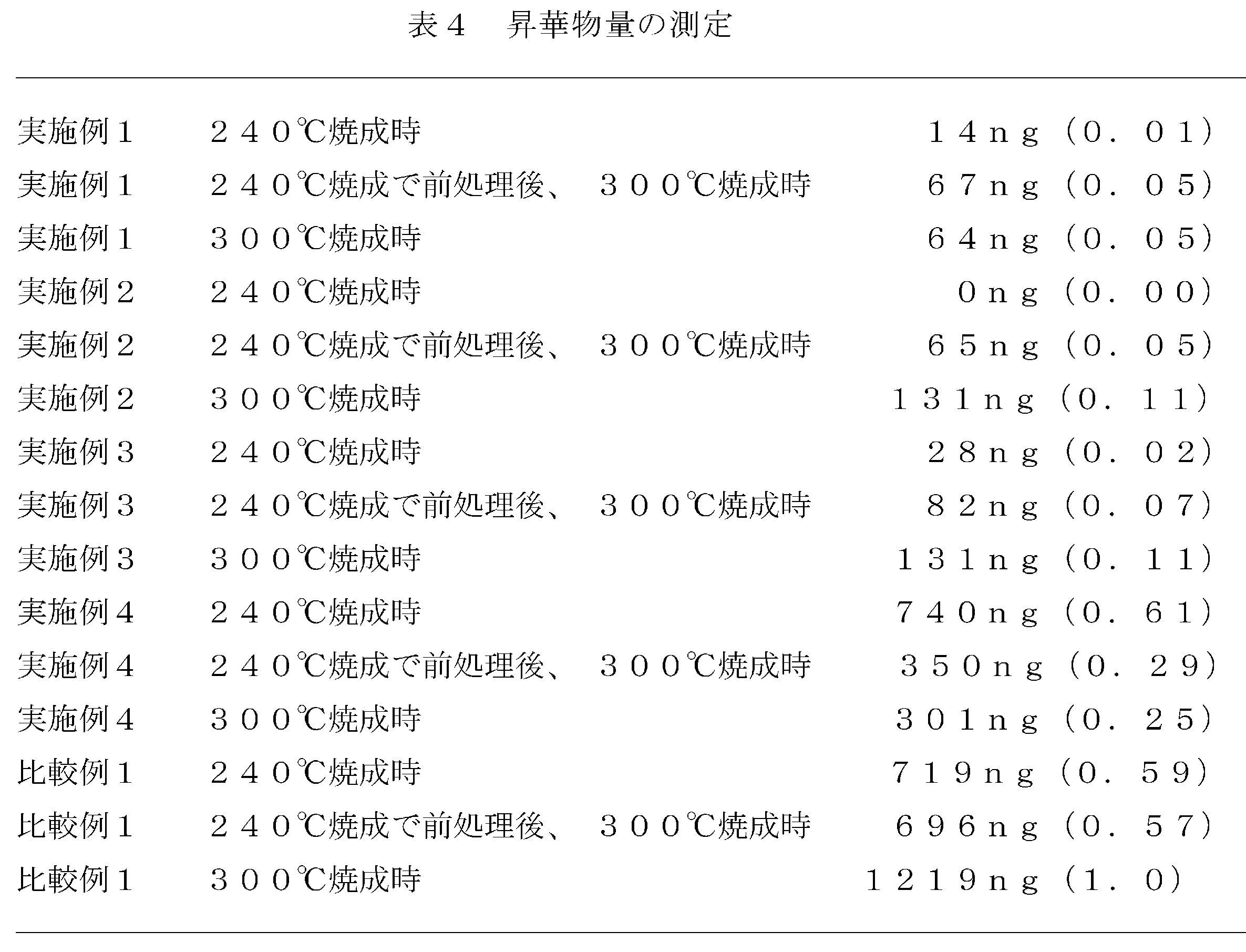
- Table 4 the amount of sublimation shown by the measuring devices from 0 to 180 seconds in Examples 1 to 4 and Comparative Example 1 is shown as the sublimation amount and the sublimation amount ratio.
- the numerical value in parentheses is the sublimate amount ratio, and the sublimate amount ratio is a value normalized with the sublimation transfer amount generated from the lower layer film (300 ° C. fired film) of Comparative Example 1 as 1.
- the resist underlayer film obtained from Example 1 showed high coating uniformity.
- the present invention can provide a resist underlayer film for lithography that does not cause intermixing with a resist layer, has high dry etching resistance, has high heat resistance, and has a low amount of sublimation.
Landscapes
- Chemical & Material Sciences (AREA)
- Physics & Mathematics (AREA)
- General Physics & Mathematics (AREA)
- Health & Medical Sciences (AREA)
- Organic Chemistry (AREA)
- Engineering & Computer Science (AREA)
- Chemical Kinetics & Catalysis (AREA)
- Medicinal Chemistry (AREA)
- Polymers & Plastics (AREA)
- Structural Engineering (AREA)
- Architecture (AREA)
- Toxicology (AREA)
- Materials Engineering (AREA)
- Wood Science & Technology (AREA)
- Life Sciences & Earth Sciences (AREA)
- Materials For Photolithography (AREA)
- Spectroscopy & Molecular Physics (AREA)
- Exposure And Positioning Against Photoresist Photosensitive Materials (AREA)
- Phenolic Resins Or Amino Resins (AREA)
- Exposure Of Semiconductors, Excluding Electron Or Ion Beam Exposure (AREA)
Abstract
Description

(式(1)中、Aは少なくとも2個のアミノ基を有する2価の基であって、該基は縮合環構造を有し且つ該縮合環上の水素原子を置換する芳香族基を有する化合物から誘導される基であり、B1、B2はそれぞれ独立に水素原子、アルキル基、ベンゼン環基、縮合環基又はそれらの組み合わせを示すかまたは、B1とB2はそれらが結合する炭素原子と一緒になって環を形成しても良い。)で表される単位構造を含むポリマーを含むレジスト下層膜形成組成物、
第2観点として、式(1)中、Aがインドロカルバゾール構造を有する化合物から誘導される2価基である第1観点に記載のレジスト下層膜形成組成物、
第3観点として、インドロカルバゾール構造を有する化合物の縮合環上の水素原子を置換する芳香族基がフェニル基である第2観点に記載のレジスト下層膜形成組成物、
第4観点として、式(1)中、Aが式(2):
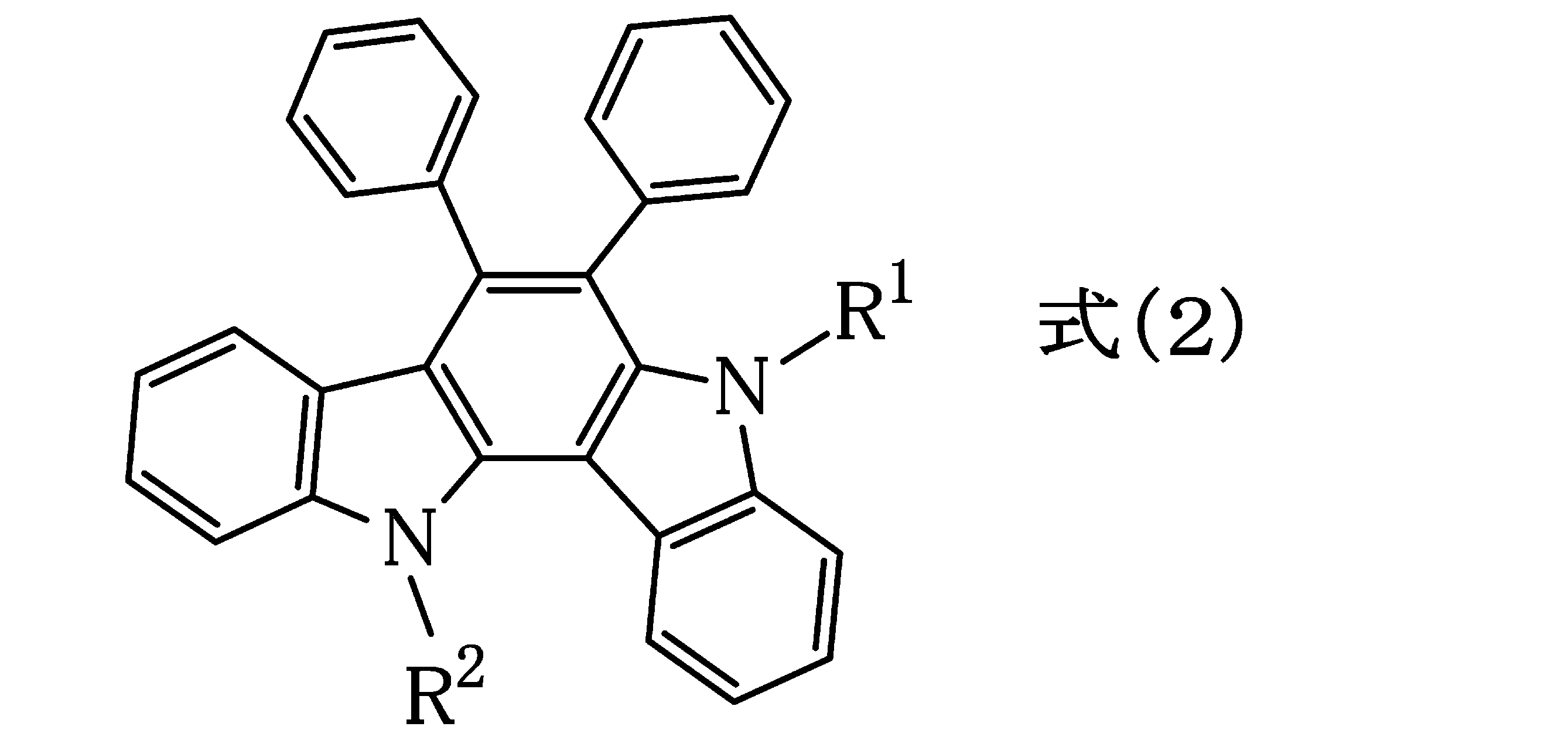
(式(2)中、R1及びR2はそれぞれ独立に水素原子、炭素原子数1乃至10のアルキル基、又は炭素原子数6乃至40のアリール基を示す。)で表される化合物から誘導される2価基である第1観点に記載のレジスト下層膜形成組成物、
第5観点として、式(2)で表される化合物が、インドールとベンジルとを酸化合物の存在下で反応させて得られる反応物である第4観点に記載のレジスト下層膜形成組成物。
第6観点として、更に架橋剤を含む第1観点乃至第5観点のいずれか一つに記載のレジスト下層膜形成組成物、
第7観点として、更に酸及び/又は酸発生剤を含む第1観点乃至第6観点のいずれか一つに記載のレジスト下層膜形成組成物、
第8観点として、第1観点乃至第7観点のいずれか一つに記載のレジスト下層膜形成組成物を半導体基板上に塗布し焼成することによって得られるレジスト下層膜の製造方法、
第9観点として、半導体基板上に第1観点乃至第7観点のいずれか一つに記載のレジスト下層膜形成組成物からレジスト下層膜を形成する工程、その上にレジスト膜を形成する工程、光又は電子線の照射と現像によりレジストパターンを形成する工程、形成されたレジストパターンにより該レジスト下層膜をエッチングする工程、及びパターン化されたレジスト下層膜により半導体基板を加工する工程を含む半導体装置の製造方法、
第10観点として、半導体基板上に第1観点乃至第7観点のいずれか一つに記載のレジスト下層膜形成組成物からレジスト下層膜を形成する工程、その上にハードマスクを形成する工程、更にその上にレジスト膜を形成する工程、光又は電子線の照射と現像によりレジストパターンを形成する工程、形成されたレジストパターンにより該ハードマスクをエッチングする工程、パターン化されたハードマスクにより該レジスト下層膜をエッチングする工程、及びパターン化されたレジスト下層膜により半導体基板を加工する工程を含む半導体装置の製造方法、及び
第11観点として、 式(1)
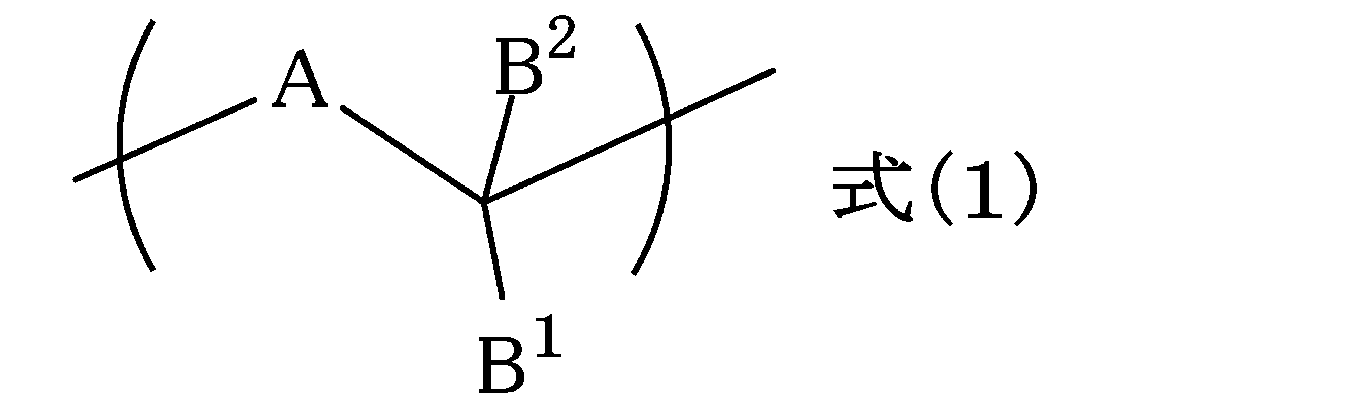
〔式(1)中、Aが式(2)
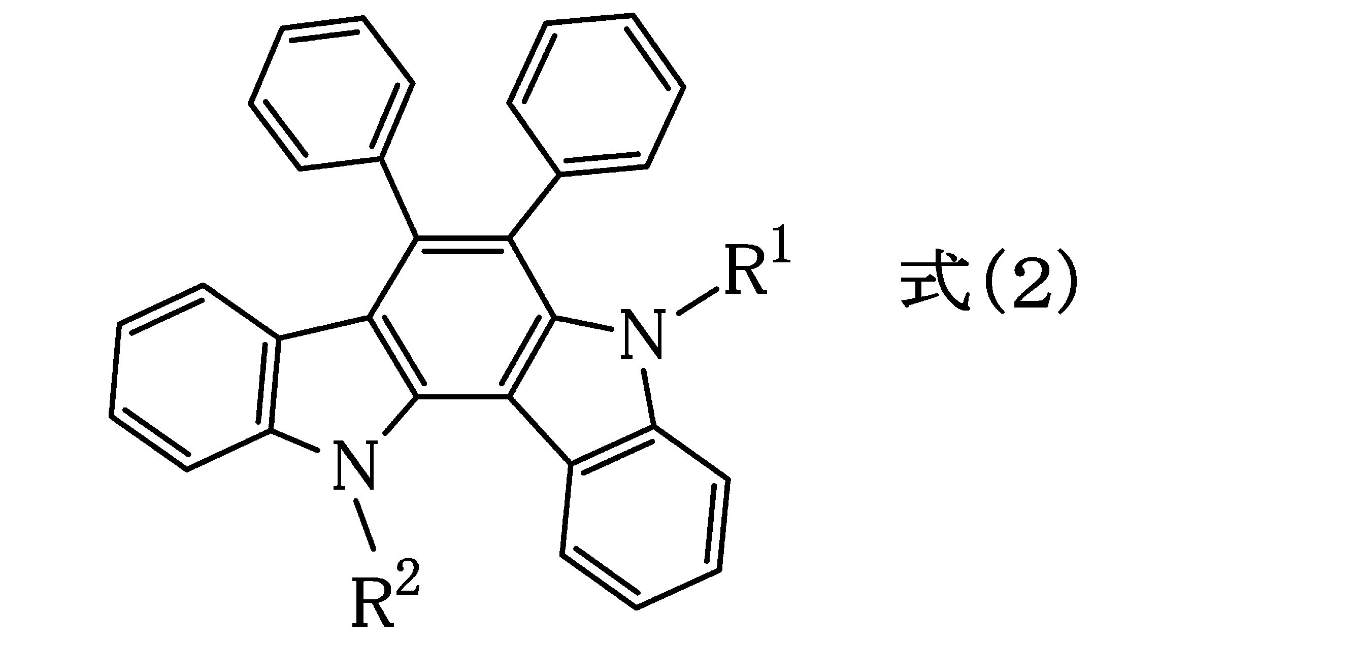
(式(2)中、R1及びR2はそれぞれ独立に水素原子、炭素原子数1乃至10のアルキル基、又は炭素原子数6乃至40のアリール基を示す。)で表される化合物から誘導される2価基を示し、B1、B2はそれぞれ独立に水素原子、アルキル基、ベンゼン環基、縮合環基又はそれらの組み合わせを示すかまたは、B1とB2はそれらが結合する炭素原子と一緒になって環を形成しても良い。〕で表される単位構造を有するポリマーである。
本発明のレジスト下層膜形成組成物には基板からの反射を効率的に抑制する性能を付与することも可能であり、露光光の反射防止膜としての効果を合わせ持つこともできる。
本発明のレジスト下層膜形成組成物により、レジストに近いドライエッチング速度の選択比、レジストに比べて小さいドライエッチング速度の選択比や半導体基板に比べて小さいドライエッチング速度の選択比を持つ、優れたレジスト下層膜を提供することができる。
レジストパターンの微細化に伴いレジストパターンが現像後に倒れることを防止するためにレジストの薄膜化が行われている。そのような薄膜レジストでは、レジストパターンをエッチングプロセスでその下層膜に転写し、その下層膜をマスクとして基板加工を行うプロセスや、レジストパターンをエッチングプロセスでその下層膜に転写し、さらに下層膜に転写されたパターンを異なるガス組成を用いてその下層膜に転写するという行程を繰り返し、最終的に基板加工を行うプロセスがある。本発明のレジスト下層膜及びその形成組成物はこのプロセスに有効である。
本発明では上記ポリマーと溶剤を含む。そして、架橋剤と酸を含むことができ、必要に応じて酸発生剤、界面活性剤等の添加剤を含むことができる。この組成物の固形分は0.1乃至70質量%、または0.1乃至60質量%である。固形分はレジスト下層膜形成組成物から溶剤を除いた全成分の含有割合である。固形分中に上記ポリマーを1乃至100質量%、または1乃至99.9質量%、または50乃至99.9質量%の割合で含有することができる。
本発明に用いられるポリマーは、重量平均分子量が600乃至1000000、又は600乃至200000である。
インドロカルバゾール構造の縮合環上の水素原子を置換する芳香族基は、例えばフェニル基、ナフチル基、アントリル基、ピレン基等が挙げられるが、フェニル基を好ましく用いることができる。
上記式(2)で表される化合物はR1とR2が水素原子の場合にジフェニルインドロカルバゾールであり、また窒素上の水素原子を置換する置換基を有するその誘導体が挙げられる。上記ジフェニルインドロカルバゾールは2モルのインドールに対して1モルのベンジルを酸触媒の存在下に反応させ得ることができる。酸触媒としてはメタンスルホン酸、p-トルエンスルホン酸、p-トルエンスルホン酸一水和物等の有機スルホン酸類を好ましく用いることができる。トルエン等の炭化水素溶剤を用い、140乃至180℃程度の温度で50乃至20時間の還流を行うことで合成することができる。
式(2)中、R1及びR2はそれぞれ独立に水素原子、炭素原子数1乃至10のアルキル基、又は炭素原子数6乃至40のアリール基を示すことができる。特に水素原子を用いることができる。
B1、B2はそれぞれ式(1)で表される単位構造を有するポリマーの製造の際原料となる、水素原子、アルキル基、ベンゼン環基、縮合環基を有するアルデヒド又はケトンに由来する基であり、Aに相当する部分を提供する化合物との間でノボラック樹脂を形成する。
式(1)で表される単位構造は以下に例示することができる。
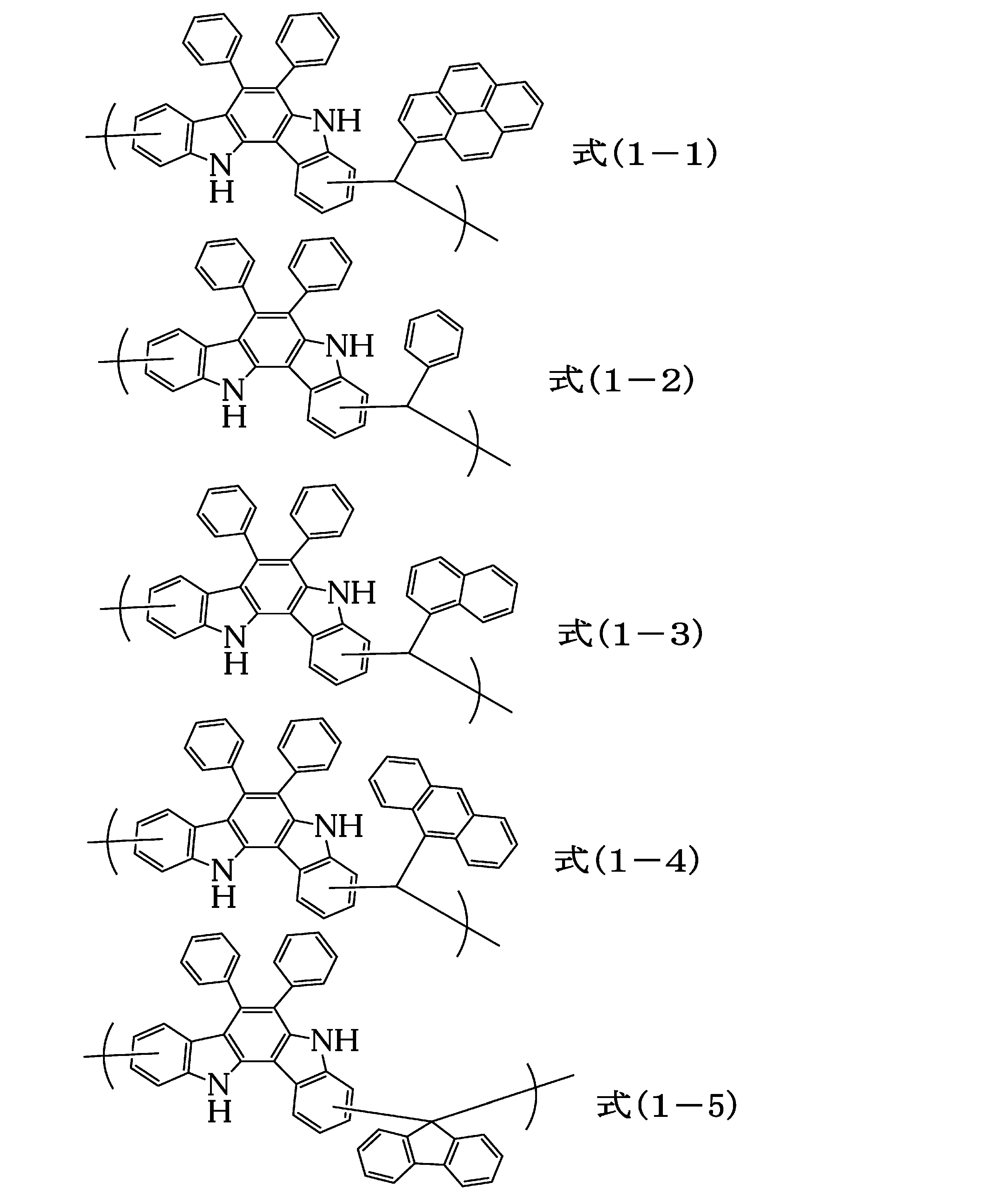
また、上記架橋剤としては耐熱性の高い架橋剤を用いることができる。耐熱性の高い架橋剤としては分子内に芳香族環(例えば、ベンゼン環、ナフタレン環)を有する架橋形成置換基を含有する化合物を好ましく用いることができる。

式(3)中、R3及びR4はそれぞれ独立に水素原子、炭素数1乃至10のアルキル基、又は炭素数6乃至20のアリール基であり、n1は1乃至4の整数であり、n2は1乃至(5-n1)の整数であり、(n1+n2)は2乃至5の整数を示す。
式(4)中、R5は水素原子又は炭素数1乃至10のアルキル基であり、R6は炭素数1乃至10のアルキル基であり、n3は1乃至4の整数であり、n4は0乃至(4-n3)であり、(n3+n4)は1乃至4の整数を示す。オリゴマー及びポリマーは繰り返し単位構造の数が2乃至100、又は2乃至50の範囲で用いることができる。
これらのアルキル基及びアリール基は、上記アルキル基及びアリール基を例示することができる。


更なる吸光剤としては例えば、「工業用色素の技術と市場」(CMC出版)や「染料便覧」(有機合成化学協会編)に記載の市販の吸光剤、例えば、C.I.DisperseYellow1,3,4,5,7,8,13,23,31,49,50,51,54,60,64,66,68,79,82,88,90,93,102,114及び124;C.I.DisperseOrange1,5,13,25,29,30,31,44,57,72及び73;C.I.DisperseRed1,5,7,13,17,19,43,50,54,58,65,72,73,88,117,137,143,199及び210;C.I.DisperseViolet43;C.I.DisperseBlue96;C.I.FluorescentBrighteningAgent112,135及び163;C.I.SolventOrange2及び45;C.I.SolventRed1,3,8,23,24,25,27及び49;C.I.PigmentGreen10;C.I.PigmentBrown2等を好適に用いることができる。上記吸光剤は通常、リソグラフィー用レジスト下層組成物の全固形分に対して10質量%以下、好ましくは5質量%以下の割合で配合される。
1L三口フラスコに30.00gのベンジル(東京化成工業株式会社製)、41.79gのインドール(東京化成工業株式会社製)、5.43gのp-トルエンスルホン酸一水和物(東京化成工業株式会社製)、300gのトルエン(関東化学株式会社製)を入れた。その後、還流管を取り付け、窒素雰囲気下、160℃で約12時間還流撹拌した。反応終了後、沈殿物を吸引濾過にて回収し、トルエン1L、メタノール1Lで洗浄した。沈殿物は60℃で約12時間真空乾燥させた。
1L三口フラスコに乾燥させた沈殿物と1,4-ジオキサン500mLを入れた。その後、還流管を取り付け、窒素雰囲気下、120℃で約1時間還流撹拌した。撹拌停止後、冷却させて再結晶を行った。再結晶した化合物を吸引濾過にて回収し、1,4-ジオキサン1L、ヘキサン1Lで洗浄した。沈殿物は60℃で約12時間真空乾燥させ、式(2-1)に示す化合物1を17.7g、収率24.6%、純度99.1%で得た。
三口フラスコに5.00gの化合物1、2.84gの1-ピレンカルボキシアルデヒド(アルドリッチ(株)製)、19.12gのプロピレングリコールモノメチルエーテルアセテート、0.35gのメタンスルホン酸(東京化成工業株式会社製)を入れた。その後150℃まで加熱し、約36時間還流撹拌した。反応終了後、プロピレングリコールモノメチルエーテルアセテート 24.80gで希釈し、沈殿物をろ過により除去した。回収したろ液をメタノール溶液中に滴下し、再沈殿させた。得られた沈殿物を吸引ろ過し、ろ物を60℃で一晩減圧乾燥した。そして、黒色粉末の樹脂を2.51g得た。得られたポリマーは式(1-1)に相当した。GPCによりポリスチレン換算で測定される重量平均分子量Mwは5,900、多分散度Mw/Mnは2.19であった。
二口フラスコに8.00gの化合物1、2.08gのベンズアルデヒド(キシダ化学株式会社製)、28.39gのプロピレングリコールモノメチルエーテルアセテート、7.10gのN-メチル-2-ピロリジノン(関東化学株式会社製)、1.13gのメタンスルホン酸(東京化成工業株式会社製)を入れた。その後150℃まで加熱し、約20時間還流撹拌した。反応終了後、プロピレングリコールモノメチルエーテルアセテート 20.49gで希釈し、沈殿物をろ過により除去した。回収したろ液をメタノール溶液中に滴下し、再沈殿させた。得られた沈殿物を吸引ろ過し、ろ物を60℃で一晩減圧乾燥した。そして、灰色粉末の樹脂を6.42g得た。得られたポリマーは式(1-2)に相当した。GPCによりポリスチレン換算で測定される重量平均分子量Mwは16,100、多分散度Mw/Mnは3.12であった。
二口フラスコに8.00gの化合物1、3.06gの1-ナフトアルデヒド(東京化成工業株式会社製)、32.83gのプロピレングリコールモノメチルエーテルアセテート、8.21gのN-メチル-2-ピロリジノン(関東化学株式会社製)、2.26gのメタンスルホン酸(東京化成工業株式会社製)を入れた。その後150℃まで加熱し、約20時間還流撹拌した。反応終了後、プロピレングリコールモノメチルエーテルアセテート 19.37gで希釈し、沈殿物をろ過により除去した。回収したろ液をメタノール溶液中に滴下し、再沈殿させた。得られた沈殿物を吸引ろ過し、ろ物を60℃で一晩減圧乾燥した。そして、灰色粉末の樹脂を6.58g得た。得られたポリマーは式(1-3)に相当した。GPCによりポリスチレン換算で測定される重量平均分子量Mwは7,500、多分散度Mw/Mnは2.02であった。
二口フラスコに9.00gの化合物1、3.97gの9-フルオレノン(東京化成工業株式会社製)、10.56gのプロピレングリコールモノメチルエーテルアセテート、4.53gのN-メチル-2-ピロリジノン(関東化学株式会社製)、2.12gのメタンスルホン酸(東京化成工業株式会社製)を入れた。その後150℃まで加熱し、約63時間還流撹拌した。反応終了後、プロピレングリコールモノメチルエーテルアセテート 34.68gで希釈し、沈殿物をろ過により除去した。回収したろ液をメタノール溶液中に滴下し、再沈殿させた。得られた沈殿物を吸引ろ過し、ろ物を60℃で一晩減圧乾燥した。そして、灰色粉末の樹脂を5.45g得た。得られたポリマーは式(1-5)に相当した。GPCによりポリスチレン換算で測定される重量平均分子量Mwは3,100、多分散度Mw/Mnは1.51であった。
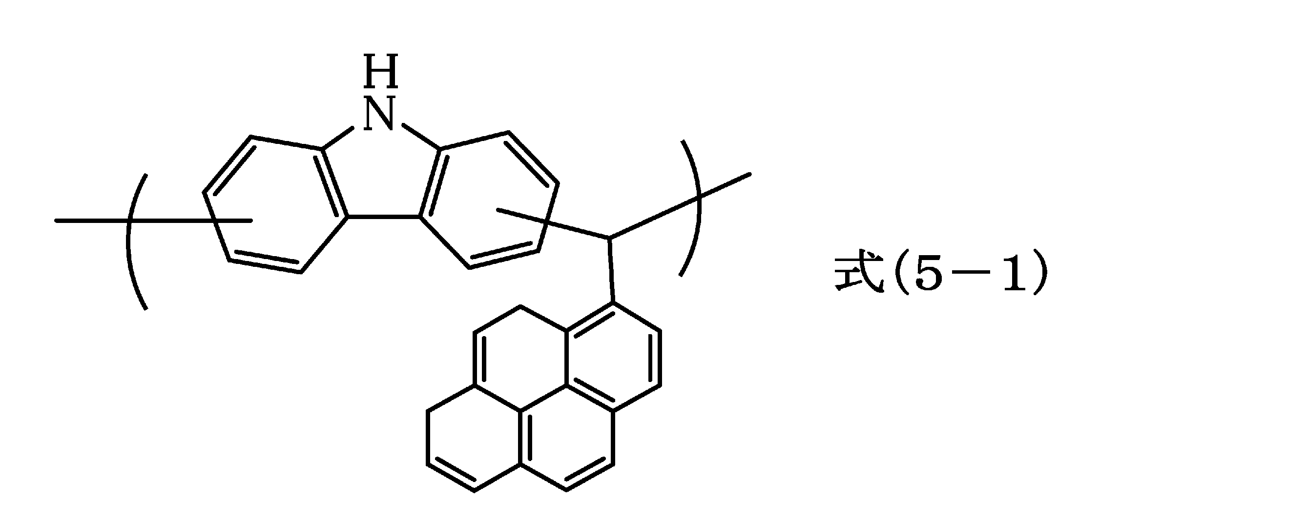
500mLナスフラスコに30.00gのカルバゾール(東京化成工業株式会社製)、41.68gの1-ピレンカルボキシアルデヒド(アルドリッチ製)、117.76gのプロピレングリコールモノメチルエーテルアセテート、6.83gのp-トルエンスルホン酸一水和物(東京化成工業株式会社製)を入れた。その後150℃まで加熱し、約1時間還流撹拌した。反応終了後、520.49gのプロピレングリコールモノメチルエーテルアセテートで希釈し、沈殿物をろ過により除去した。回収したろ液をメタノール溶液中に滴下し、再沈殿させた。得られた沈殿物を吸引ろ過し、ろ物を60℃で一晩減圧乾燥した。そして、青色粉末のカルバゾール樹脂を71.6g得た。得られたポリマーは式(5-1)に相当した。GPCによりポリスチレン換算で測定される重量平均分子量Mwは2,600、多分散度Mw/Mnは1.62であった。
合成例1で得た1.0gの樹脂(式(1-1))に、界面活性剤として0.001gのメガファックR-30Nを混合し、1.10gのプロピレングリコールモノメチルエーテルアセテート、8.14gのシクロヘキサノンに溶解させ、ろ過し多層膜によるリソグラフィープロセスに用いるレジスト下層膜形成組成物の溶液を調製した。
合成例2で得た1.0gの樹脂(式(1-2))に、界面活性剤として0.001gのメガファックR-30Nを混合し、1.10gのプロピレングリコールモノメチルエーテルアセテート、8.14gのシクロヘキサノンに溶解させ、ろ過し多層膜によるリソグラフィープロセスに用いるレジスト下層膜形成組成物の溶液を調製した。
合成例3で得た1.0gの樹脂(式(1-3))に、界面活性剤として0.001gのメガファックR-30Nを混合し、1.10gのプロピレングリコールモノメチルエーテルアセテート、8.14gのシクロヘキサノンに溶解させ、ろ過し多層膜によるリソグラフィープロセスに用いるレジスト下層膜形成組成物の溶液を調製した。
合成例4で得た1.0gの樹脂(式(1-5))に、界面活性剤として0.001gのメガファックR-30Nを混合し、1.10gのプロピレングリコールモノメチルエーテルアセテート、8.14gのシクロヘキサノンに溶解させ、ろ過し多層膜によるリソグラフィープロセスに用いるレジスト下層膜形成組成物の溶液を調製した。
比較合成例1で得た1.0gの樹脂(式(5-1))に、界面活性剤として0.001gのメガファックR-30Nを混合し、1.10gのプロピレングリコールモノメチルエーテルアセテート、8.14gのシクロヘキサノンに溶解させ、ろ過し多層膜によるリソグラフィープロセスに用いるレジスト下層膜形成組成物の溶液を調製した。
実施例1乃至4及び比較例1で調製したレジスト下層膜形成組成物の溶液を、それぞれスピンコーターを用いてシリコンウエハー上に塗布し、ホットプレート上で240℃1分間焼成し、その後400℃1分間焼成し、レジスト下層膜(膜厚0.08μm)を形成した。これらレジスト下層膜をレジストに使用する溶剤である、乳酸エチル、プロピレングリコールモノメチルエーテル、プロピレングリコールモノメチルエーテルアセテート、及びシクロヘキサノンに浸漬した。これらレジスト下層膜はこれら溶剤に不溶であった。
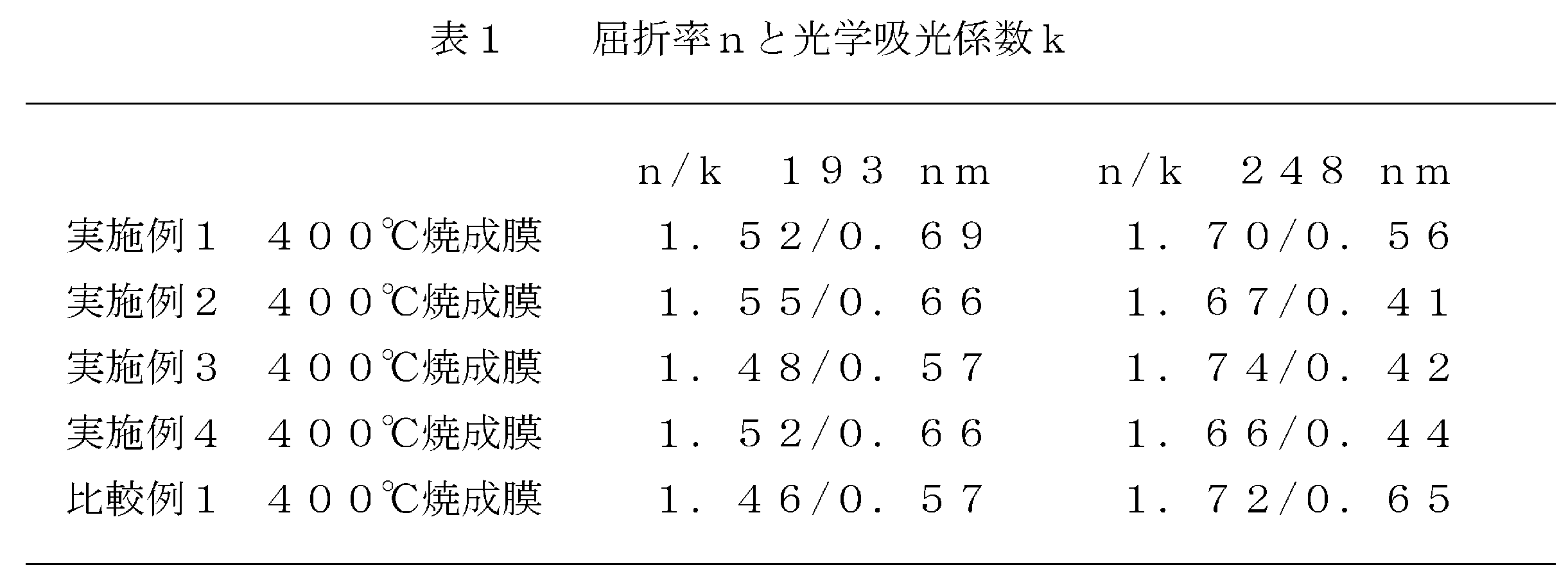
実施例1乃至4、比較例1で調製したレジスト下層膜形成組成物の溶液を、それぞれスピンコーターを用いてシリコンウエハー上に塗布した。ホットプレート上で240℃1分間焼成し、その後400℃1分間(実施例10乃至12は400℃2分間)焼成し、レジスト下層膜(膜厚0.05μm)を形成した。これらのレジスト下層膜を、分光エリプソメーターを用いて波長193nm及び248nmでの屈折率(n値)及び光学吸光係数(k値、減衰係数とも呼ぶ)を測定した。結果を表1に示した。
ドライエッチング速度の測定に用いたエッチャー及びエッチングガスは以下のものを用いた。
RIE-10NR(サムコ製):CF4
実施例1乃至4、比較例1で調製したレジスト下層膜形成組成物の溶液を、それぞれスピンコーターを用いてシリコンウエハー上に塗布した。ホットプレート上で240℃1分間焼成し、その後400℃1分間焼成してレジスト下層膜(膜厚0.20μm)を形成した。また、240℃焼成を行わずに400℃90秒焼成してレジスト下層膜(膜厚0.20μm)を形成した。エッチングガスとしてCF4ガスを使用してドライエッチング速度を測定し、実施例1乃至4と比較例1のレジスト下層膜のドライエッチング速度との比較を行った。結果を表2に示した。ドライエッチング速度比は(レジスト下層膜)/(KrFフォトレジスト)のドライエッチング速度比である。

実施例1乃至4及び比較例1で調製したレジスト下層膜形成組成物の溶液を、それぞれスピンコーターを用いてシリコンウエハー上に塗布し、ホットプレート上で400℃90秒間焼成して、レジスト下層膜(膜厚0.25μm)を形成した。得られた膜を室温(約20℃)から一分間に10℃ずつの割合で昇温加熱して大気中で熱重量分析を行い、重量減少の経時変化を追跡した。結果を表3に示す。
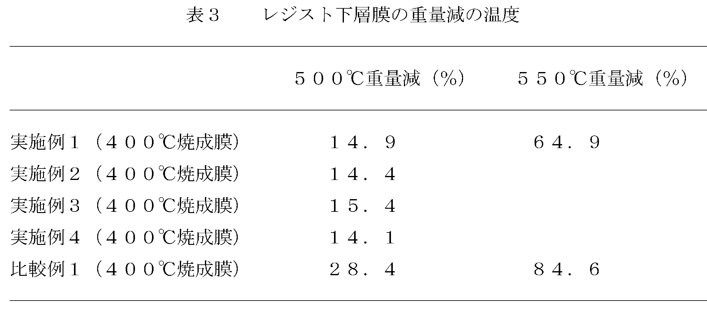
実施例2乃至実施例4は500℃重量減の測定で差異が観測されたので500℃までの測定データとした。
昇華物量の測定は国際公開WO2007/111147パンフレットに記載されている昇華物量測定装置を用いて実施した。直径4インチのシリコンウエハー基板に、実施例1乃至4及び比較例1で調製したレジスト下層膜形成組成物をそれぞれ塗布し、240℃焼成評価サンプルと300℃焼成評価サンプルは焼成せず、240℃焼成で前処理後に300℃焼成で評価するサンプルは240℃で1分間焼成し、レジスト下層膜(膜厚0.05μm)を形成した。レジスト下層膜が塗布されたウエハーを、ホットプレートが一体化した昇華物量測定装置にセットして、120秒間ベークし、昇華物をQCM(Quartz Crystal Microbalance)センサー、すなわち電極が形成された水晶振動子に捕集した。QCMセンサーは、水晶振動子の表面(電極)に昇華物が付着するとその質量に応じて水晶振動子の周波数が変化する(下がる)性質を利用して、微量の質量変化を測定することができる。
なお、前記昇華物量測定装置のQCMセンサーと捕集ロート部分の接続となるフローアタッチメント(検出部分)にはノズルをつけずに使用し、そのため、センサー(水晶振動子)との距離が30mmのチャンバーユニットの流路(口径:32mm)から、気流が絞られることなく流入する。また、QCMセンサーには、電極として珪素とアルミニウムを主成分とする材料(AlSi)を用い、水晶振動子の直径(センサー直径)が14mm、水晶振動子表面の電極直径が5mm、共振周波数が9MHzのものを用いた。
実施例1及び比較例1で調製したレジスト下層膜形成組成物の溶液を、それぞれスピンコーターを用いてシリコンウエハー上に塗布し、ホットプレート上で240℃1分間その後、400℃1分間焼成して、レジスト下層膜(膜厚0.34μm)を形成した。これらの面内均一性を測定した結果を表5に示す。
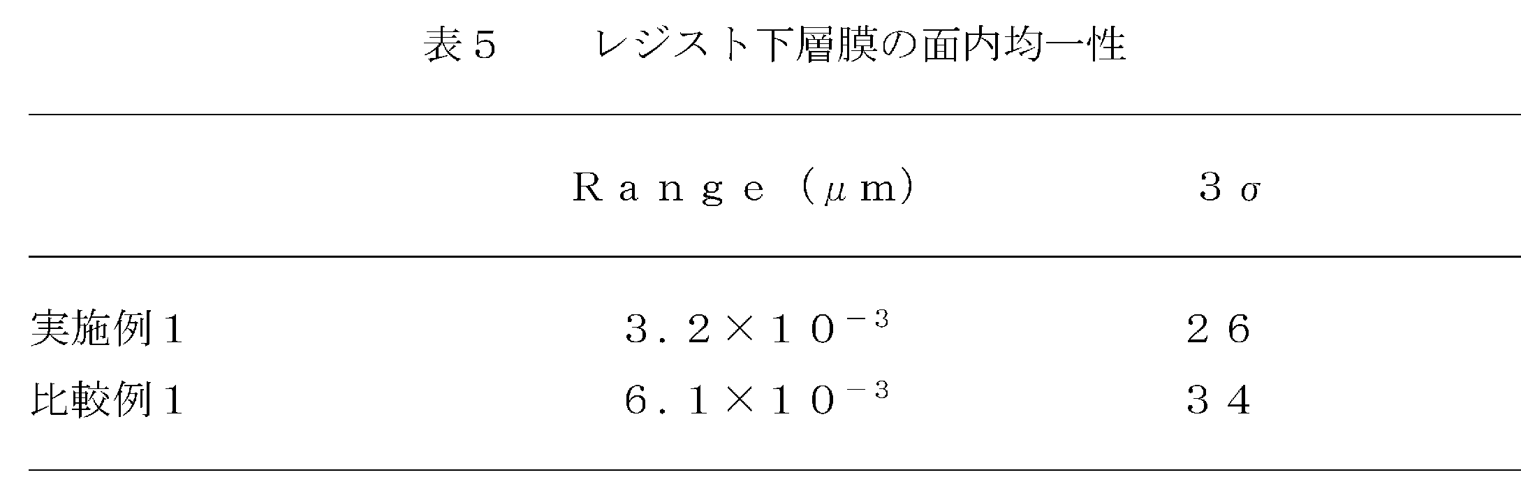
実施例1から得られたレジスト下層膜は高い塗布均一性を示した。
Claims (11)
- 下記式(1):
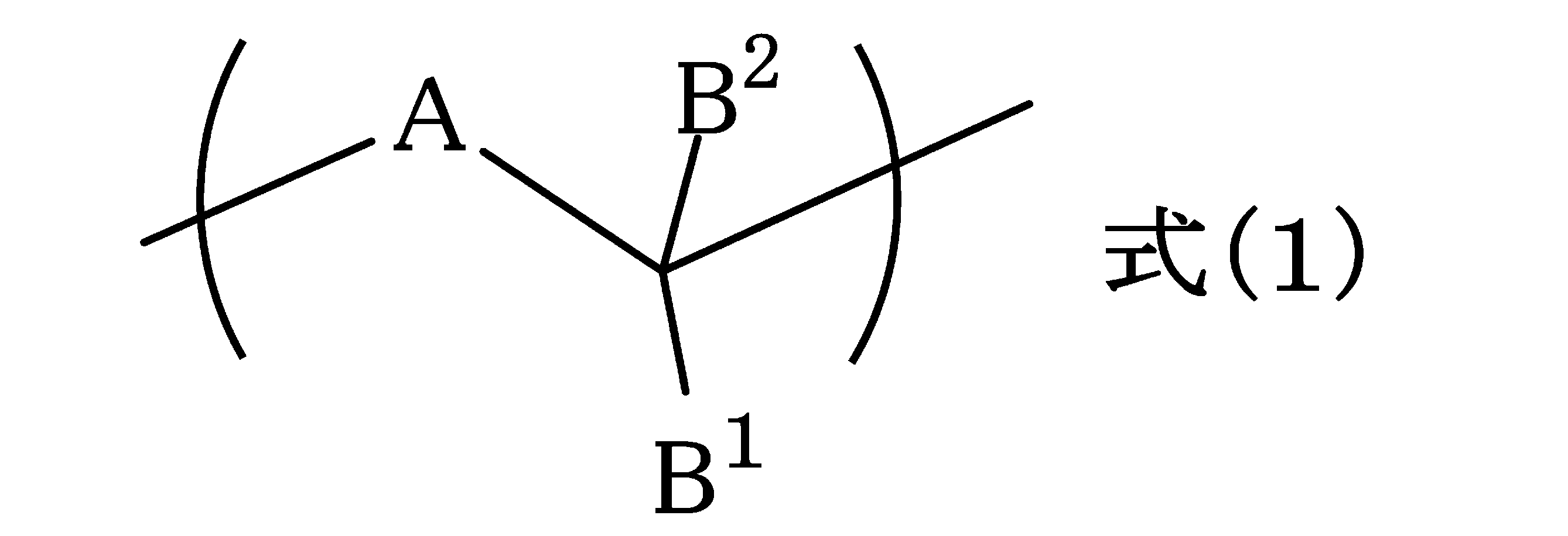
(式(1)中、Aは少なくとも2個のアミノ基を有する2価の基であって、該基は縮合環構造を有し且つ該縮合環上の水素原子を置換する芳香族基を有する化合物から誘導される基であり、B1、B2はそれぞれ独立に水素原子、アルキル基、ベンゼン環基、縮合環基又はそれらの組み合わせを示すかまたは、B1とB2はそれらが結合する炭素原子と一緒になって環を形成しても良い。)で表される単位構造を含むポリマーを含むレジスト下層膜形成組成物。 - 式(1)中、Aがインドロカルバゾール構造を有する化合物から誘導される2価基である請求項1に記載のレジスト下層膜形成組成物。
- インドロカルバゾール構造を有する化合物の縮合環上の水素原子を置換する芳香族基がフェニル基である請求項2に記載のレジスト下層膜形成組成物。
- 式(1)中、Aが式(2):
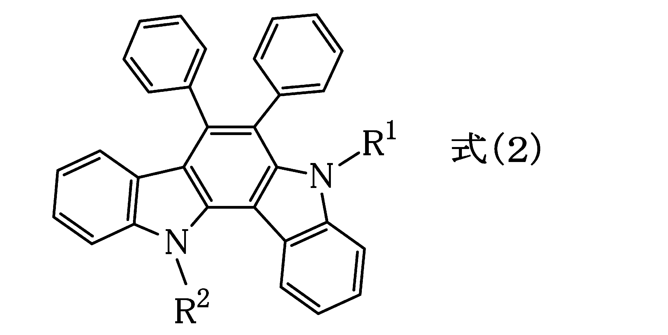
(式(2)中、R1及びR2はそれぞれ独立に水素原子、炭素原子数1乃至10のアルキル基、又は炭素原子数6乃至40のアリール基を示す。)で表される化合物から誘導される2価基である請求項1に記載のレジスト下層膜形成組成物。 - 式(2)で表される化合物が、インドールとベンジルとを酸化合物の存在下で反応させて得られる反応物である請求項4に記載のレジスト下層膜形成組成物。
- 更に架橋剤を含む請求項1乃至請求項5のいずれか1項に記載のレジスト下層膜形成組成物。
- 更に酸及び/又は酸発生剤を含む請求項1乃至請求項6のいずれか1項に記載のレジスト下層膜形成組成物。
- 請求項1乃至請求項7のいずれか1項に記載のレジスト下層膜形成組成物を半導体基板上に塗布し焼成することによって得られるレジスト下層膜の製造方法。
- 半導体基板上に請求項1乃至請求項7のいずれか1項に記載のレジスト下層膜形成組成物からレジスト下層膜を形成する工程、その上にレジスト膜を形成する工程、光又は電子線の照射と現像によりレジストパターンを形成する工程、形成されたレジストパターンにより該レジスト下層膜をエッチングする工程、及びパターン化されたレジスト下層膜により半導体基板を加工する工程を含む半導体装置の製造方法。
- 半導体基板上に請求項1乃至請求項7のいずれか1項に記載のレジスト下層膜形成組成物からレジスト下層膜を形成する工程、その上にハードマスクを形成する工程、更にその上にレジスト膜を形成する工程、光又は電子線の照射と現像によりレジストパターンを形成する工程、形成されたレジストパターンにより該ハードマスクをエッチングする工程、パターン化されたハードマスクにより該レジスト下層膜をエッチングする工程、及びパターン化されたレジスト下層膜により半導体基板を加工する工程を含む半導体装置の製造方法。
- 式(1)
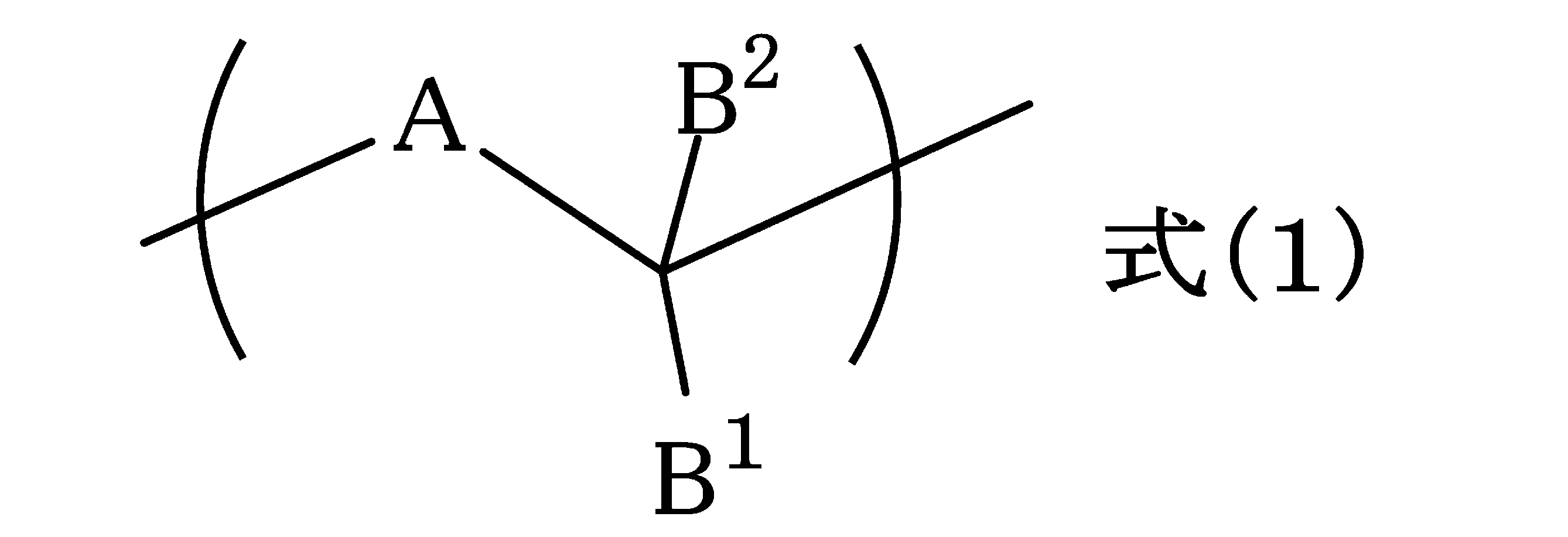
〔式(1)中、Aが式(2)
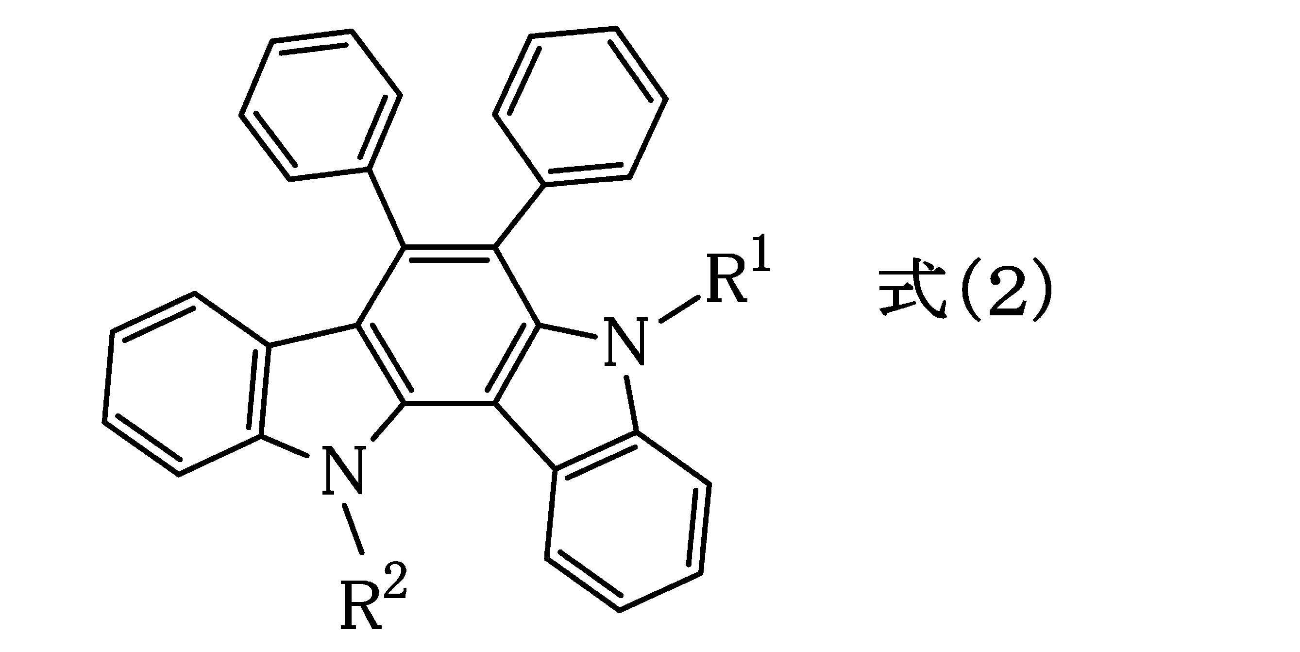
(式(2)中、R1及びR2はそれぞれ独立に水素原子、炭素原子数1乃至10のアルキル基、又は炭素原子数6乃至40のアリール基を示す。)で表される化合物から誘導される2価基を示し、B1、B2はそれぞれ独立に水素原子、アルキル基、ベンゼン環基、縮合環基又はそれらの組み合わせを示すかまたは、B1とB2はそれらが結合する炭素原子と一緒になって環を形成しても良い。)〕で表される単位構造を有するポリマー。
Priority Applications (7)
| Application Number | Priority Date | Filing Date | Title |
|---|---|---|---|
| US15/780,657 US20180356732A1 (en) | 2015-12-01 | 2016-11-30 | Resist underlayer film-forming composition containing indolocarbazole novolak resin |
| KR1020187017735A KR102634064B1 (ko) | 2015-12-01 | 2016-11-30 | 인돌로카바졸노볼락 수지를 포함하는 레지스트 하층막 형성 조성물 |
| JP2017554146A JP6781410B2 (ja) | 2015-12-01 | 2016-11-30 | インドロカルバゾールノボラック樹脂を含むレジスト下層膜形成組成物 |
| KR1020247003719A KR102820755B1 (ko) | 2015-12-01 | 2016-11-30 | 인돌로카바졸노볼락 수지를 포함하는 레지스트 하층막 형성 조성물 |
| CN201680070329.2A CN108292098B (zh) | 2015-12-01 | 2016-11-30 | 包含吲哚并咔唑酚醛清漆树脂的抗蚀剂下层膜形成用组合物 |
| US17/880,761 US11720024B2 (en) | 2015-12-01 | 2022-08-04 | Resist underlayer film-forming composition containing indolocarbazole novolak resin |
| US18/207,934 US12242196B2 (en) | 2015-12-01 | 2023-06-09 | Resist underlayer film-forming composition containing indolocarbazole novolak resin |
Applications Claiming Priority (2)
| Application Number | Priority Date | Filing Date | Title |
|---|---|---|---|
| JP2015235002 | 2015-12-01 | ||
| JP2015-235002 | 2015-12-01 |
Related Child Applications (2)
| Application Number | Title | Priority Date | Filing Date |
|---|---|---|---|
| US15/780,657 A-371-Of-International US20180356732A1 (en) | 2015-12-01 | 2016-11-30 | Resist underlayer film-forming composition containing indolocarbazole novolak resin |
| US17/880,761 Division US11720024B2 (en) | 2015-12-01 | 2022-08-04 | Resist underlayer film-forming composition containing indolocarbazole novolak resin |
Publications (1)
| Publication Number | Publication Date |
|---|---|
| WO2017094780A1 true WO2017094780A1 (ja) | 2017-06-08 |
Family
ID=58797347
Family Applications (1)
| Application Number | Title | Priority Date | Filing Date |
|---|---|---|---|
| PCT/JP2016/085561 Ceased WO2017094780A1 (ja) | 2015-12-01 | 2016-11-30 | インドロカルバゾールノボラック樹脂を含むレジスト下層膜形成組成物 |
Country Status (6)
| Country | Link |
|---|---|
| US (3) | US20180356732A1 (ja) |
| JP (1) | JP6781410B2 (ja) |
| KR (2) | KR102634064B1 (ja) |
| CN (1) | CN108292098B (ja) |
| TW (1) | TWI765872B (ja) |
| WO (1) | WO2017094780A1 (ja) |
Cited By (9)
| Publication number | Priority date | Publication date | Assignee | Title |
|---|---|---|---|---|
| WO2018043410A1 (ja) * | 2016-09-01 | 2018-03-08 | 日産化学工業株式会社 | トリアリールジアミン含有ノボラック樹脂を含むレジスト下層膜形成組成物 |
| KR20190024779A (ko) | 2017-08-30 | 2019-03-08 | 신에쓰 가가꾸 고교 가부시끼가이샤 | 유기막 형성용 조성물, 반도체 장치 제조용 기판, 유기막의 형성 방법, 패턴 형성 방법 및 중합체 |
| KR20190024785A (ko) | 2017-08-28 | 2019-03-08 | 신에쓰 가가꾸 고교 가부시끼가이샤 | 유기막 형성용 조성물, 반도체 장치 제조용 기판, 유기막의 형성 방법, 패턴 형성 방법 및 중합체 |
| JP2019062057A (ja) * | 2017-09-26 | 2019-04-18 | 富士フイルム株式会社 | インプリント用下層膜形成用組成物、キット、積層体、積層体の製造方法、硬化物パターンの製造方法、回路基板の製造方法 |
| WO2019132178A1 (ko) * | 2017-12-26 | 2019-07-04 | 삼성에스디아이 주식회사 | 중합체, 유기막 조성물 및 패턴 형성 방법 |
| WO2019225614A1 (ja) * | 2018-05-25 | 2019-11-28 | 日産化学株式会社 | 環式カルボニル化合物を用いたレジスト下層膜形成組成物 |
| EP3761115A1 (en) | 2019-07-05 | 2021-01-06 | Shin-Etsu Chemical Co., Ltd. | Composition for forming organic film, substrate for manufacturing semiconductor device, method for forming organic film, patterning process, and polymer |
| WO2024096069A1 (ja) * | 2022-11-02 | 2024-05-10 | 日産化学株式会社 | レジスト下層膜形成組成物 |
| WO2024172128A1 (ja) * | 2023-02-16 | 2024-08-22 | 日産化学株式会社 | レジスト下層膜形成組成物 |
Families Citing this family (6)
| Publication number | Priority date | Publication date | Assignee | Title |
|---|---|---|---|---|
| US20180356732A1 (en) * | 2015-12-01 | 2018-12-13 | Nissan Chemical Industries, Ltd. | Resist underlayer film-forming composition containing indolocarbazole novolak resin |
| KR102109919B1 (ko) * | 2019-01-18 | 2020-05-12 | 주식회사 오라스 | 반사방지용 하드마스크 조성물 |
| CN114341743A (zh) * | 2019-09-17 | 2022-04-12 | Jsr株式会社 | 组合物、抗蚀剂底层膜、抗蚀剂底层膜的形成方法、经图案化的基板的制造方法及化合物 |
| CN110845503B (zh) * | 2019-11-25 | 2022-04-22 | 南京林业大学 | 一种芳胺取代苯并二吲哚类有机空穴传输材料的制备及应用 |
| WO2024090369A1 (ja) | 2022-10-26 | 2024-05-02 | 株式会社Adeka | 化合物、組成物、硬化物、硬化物の製造方法及び電子部品の製造方法 |
| KR102894059B1 (ko) * | 2024-03-20 | 2025-12-02 | 주식회사 켐폴 | 새로운 방향족 축합 고분자 화합물 및 레지스트 하층막 조성물 |
Citations (4)
| Publication number | Priority date | Publication date | Assignee | Title |
|---|---|---|---|---|
| WO2006132088A1 (ja) * | 2005-06-10 | 2006-12-14 | Nissan Chemical Industries, Ltd. | ナフタレン樹脂誘導体を含有するリソグラフィー用塗布型下層膜形成組成物 |
| JP2008501985A (ja) * | 2004-03-25 | 2008-01-24 | エイゼット・エレクトロニック・マテリアルズ・ユーエスエイ・コーポレイション | 光結像性ポジ型底面反射防止膜 |
| WO2008126804A1 (ja) * | 2007-04-06 | 2008-10-23 | Nissan Chemical Industries, Ltd. | レジスト下層膜形成組成物 |
| JP2014029435A (ja) * | 2012-07-31 | 2014-02-13 | Nissan Chem Ind Ltd | カルボニル基含有カルバゾールノボラックを含むリソグラフィー用レジスト下層膜形成組成物 |
Family Cites Families (30)
| Publication number | Priority date | Publication date | Assignee | Title |
|---|---|---|---|---|
| JP3441102B2 (ja) | 1993-02-05 | 2003-08-25 | 京セラケミカル株式会社 | エポキシ樹脂組成物および半導体封止装置 |
| JP3645694B2 (ja) | 1997-07-25 | 2005-05-11 | 住友ベークライト株式会社 | 難燃性樹脂組成物 |
| TWI414893B (zh) * | 2006-03-14 | 2013-11-11 | Jsr Corp | 底層膜形成用組成物及圖型之形成方法 |
| US8592134B2 (en) * | 2007-12-07 | 2013-11-26 | Mitsubishi Gas Chemical Company, Inc. | Composition for forming base film for lithography and method for forming multilayer resist pattern |
| JP2009173845A (ja) | 2008-01-28 | 2009-08-06 | Panasonic Electric Works Co Ltd | 半導体封止用エポキシ樹脂組成物とそれを用いた半導体装置 |
| KR101860385B1 (ko) | 2009-06-19 | 2018-05-23 | 닛산 가가쿠 고교 가부시키 가이샤 | 카바졸 노볼락 수지 |
| US20120095132A1 (en) | 2010-10-19 | 2012-04-19 | Chung-Hao Chang | Halogen- and phosphorus-free thermosetting resin composition |
| JP5867732B2 (ja) | 2010-12-09 | 2016-02-24 | 日産化学工業株式会社 | 水酸基含有カルバゾールノボラック樹脂を含むレジスト下層膜形成組成物 |
| CN103635858B (zh) * | 2011-07-07 | 2017-09-29 | 日产化学工业株式会社 | 包含含有脂环式骨架的咔唑树脂的形成抗蚀剂下层膜的组合物 |
| CN103649835B (zh) | 2011-08-04 | 2018-02-06 | 日产化学工业株式会社 | 具有缩合系聚合物的形成euv光刻用抗蚀剂下层膜的组合物 |
| CN103827159B (zh) | 2011-09-29 | 2016-07-06 | 日产化学工业株式会社 | 二芳基胺酚醛清漆树脂 |
| US9261790B2 (en) | 2012-02-01 | 2016-02-16 | Nissan Chemical Industries, Ltd. | Resist underlayer film-forming composition containing copolymer resin having heterocyclic ring |
| US8993215B2 (en) | 2012-03-27 | 2015-03-31 | Nissan Chemical Industries, Ltd. | Resist underlayer film forming composition containing phenylindole-containing novolac resin |
| US10200844B2 (en) | 2012-08-23 | 2019-02-05 | Nokia Solutions And Networks Oy | Massive discovery of devices |
| KR102195151B1 (ko) | 2012-09-07 | 2020-12-24 | 닛산 가가쿠 가부시키가이샤 | 리소그래피용 레지스트 상층막 형성 조성물 및 이를 이용한 반도체 장치의 제조방법 |
| WO2014185335A1 (ja) | 2013-05-13 | 2014-11-20 | 日産化学工業株式会社 | ビスフェノールアルデヒドを用いたノボラック樹脂含有レジスト下層膜形成組成物 |
| US20160147151A1 (en) | 2013-06-25 | 2016-05-26 | Nissan Chemical Industries, Ltd. | Resist underlayer film-forming composition contaning pyrrole novolac resin |
| KR102367638B1 (ko) | 2014-03-31 | 2022-02-28 | 닛산 가가쿠 가부시키가이샤 | 방향족 비닐화합물이 부가된 노볼락수지를 포함하는 레지스트 하층막 형성 조성물 |
| KR102417838B1 (ko) | 2014-08-08 | 2022-07-06 | 닛산 가가쿠 가부시키가이샤 | 방향족 메틸올 화합물이 반응된 노볼락 수지를 포함하는 레지스트 하층막 형성 조성물 |
| KR101788091B1 (ko) * | 2014-09-30 | 2017-11-15 | 삼성에스디아이 주식회사 | 중합체, 유기막 조성물, 유기막, 및 패턴형성방법 |
| CN107077071B (zh) | 2014-11-04 | 2020-10-02 | 日产化学工业株式会社 | 包含具有亚芳基的聚合物的抗蚀剂下层膜形成用组合物 |
| US9873815B2 (en) | 2015-04-30 | 2018-01-23 | Samsung Sdi Co., Ltd. | Polymer, organic layer composition, and method of forming patterns |
| KR101884447B1 (ko) | 2015-07-06 | 2018-08-01 | 삼성에스디아이 주식회사 | 모노머, 유기막 조성물, 유기막, 및 패턴형성방법 |
| JP6625934B2 (ja) | 2015-07-14 | 2019-12-25 | 信越化学工業株式会社 | レジスト下層膜材料、パターン形成方法、及び化合物 |
| WO2017069063A1 (ja) | 2015-10-19 | 2017-04-27 | 日産化学工業株式会社 | 長鎖アルキル基含有ノボラックを含むレジスト下層膜形成組成物 |
| US20180356732A1 (en) * | 2015-12-01 | 2018-12-13 | Nissan Chemical Industries, Ltd. | Resist underlayer film-forming composition containing indolocarbazole novolak resin |
| KR101770749B1 (ko) | 2016-01-11 | 2017-08-23 | 최상준 | 반사방지용 하드마스크 조성물 |
| CN109643065B (zh) | 2016-09-01 | 2022-07-12 | 日产化学株式会社 | 包含含有三芳基二胺的酚醛清漆树脂的抗蚀剂下层膜形成用组合物 |
| JP6726142B2 (ja) | 2017-08-28 | 2020-07-22 | 信越化学工業株式会社 | 有機膜形成用組成物、半導体装置製造用基板、有機膜の形成方法、パターン形成方法、及び重合体 |
| JP7161451B2 (ja) | 2019-07-05 | 2022-10-26 | 信越化学工業株式会社 | 有機膜形成用組成物、半導体装置製造用基板、有機膜の形成方法、及びパターン形成方法 |
-
2016
- 2016-11-30 US US15/780,657 patent/US20180356732A1/en not_active Abandoned
- 2016-11-30 KR KR1020187017735A patent/KR102634064B1/ko active Active
- 2016-11-30 JP JP2017554146A patent/JP6781410B2/ja active Active
- 2016-11-30 KR KR1020247003719A patent/KR102820755B1/ko active Active
- 2016-11-30 CN CN201680070329.2A patent/CN108292098B/zh active Active
- 2016-11-30 WO PCT/JP2016/085561 patent/WO2017094780A1/ja not_active Ceased
- 2016-12-01 TW TW105139699A patent/TWI765872B/zh active
-
2022
- 2022-08-04 US US17/880,761 patent/US11720024B2/en active Active
-
2023
- 2023-06-09 US US18/207,934 patent/US12242196B2/en active Active
Patent Citations (4)
| Publication number | Priority date | Publication date | Assignee | Title |
|---|---|---|---|---|
| JP2008501985A (ja) * | 2004-03-25 | 2008-01-24 | エイゼット・エレクトロニック・マテリアルズ・ユーエスエイ・コーポレイション | 光結像性ポジ型底面反射防止膜 |
| WO2006132088A1 (ja) * | 2005-06-10 | 2006-12-14 | Nissan Chemical Industries, Ltd. | ナフタレン樹脂誘導体を含有するリソグラフィー用塗布型下層膜形成組成物 |
| WO2008126804A1 (ja) * | 2007-04-06 | 2008-10-23 | Nissan Chemical Industries, Ltd. | レジスト下層膜形成組成物 |
| JP2014029435A (ja) * | 2012-07-31 | 2014-02-13 | Nissan Chem Ind Ltd | カルボニル基含有カルバゾールノボラックを含むリソグラフィー用レジスト下層膜形成組成物 |
Non-Patent Citations (1)
| Title |
|---|
| NAIR, VIJAY: "An efficient synthesis of indolo[3, 2-a]carbazoles via the novel acid catalyzed reaction of indoles and diaryl-1, 2-diones", ORGANIC & BIOMOLECULAR CHEMISTRY, vol. 6, no. 10, 1 May 2008 (2008-05-01), pages 1738 - 1742, XP055238463 * |
Cited By (17)
| Publication number | Priority date | Publication date | Assignee | Title |
|---|---|---|---|---|
| WO2018043410A1 (ja) * | 2016-09-01 | 2018-03-08 | 日産化学工業株式会社 | トリアリールジアミン含有ノボラック樹脂を含むレジスト下層膜形成組成物 |
| US11300879B2 (en) | 2016-09-01 | 2022-04-12 | Nissan Chemical Corporation | Resist underlayer film forming composition containing triaryldiamine-containing novolac resin |
| US10998197B2 (en) | 2017-08-28 | 2021-05-04 | Shin-Etsu Chemical Co., Ltd. | Polymer and composition for forming organic film, substrate for manufacturing semiconductor apparatus, method for forming organic film, and patterning process |
| KR20190024785A (ko) | 2017-08-28 | 2019-03-08 | 신에쓰 가가꾸 고교 가부시끼가이샤 | 유기막 형성용 조성물, 반도체 장치 제조용 기판, 유기막의 형성 방법, 패턴 형성 방법 및 중합체 |
| KR20190024779A (ko) | 2017-08-30 | 2019-03-08 | 신에쓰 가가꾸 고교 가부시끼가이샤 | 유기막 형성용 조성물, 반도체 장치 제조용 기판, 유기막의 형성 방법, 패턴 형성 방법 및 중합체 |
| US11181821B2 (en) | 2017-08-30 | 2021-11-23 | Shin-Etsu Chemical Co., Ltd. | Composition for forming organic film, substrate for manufacturing semiconductor apparatus, method for forming organic film, patterning process, and polymer |
| JP2019062057A (ja) * | 2017-09-26 | 2019-04-18 | 富士フイルム株式会社 | インプリント用下層膜形成用組成物、キット、積層体、積層体の製造方法、硬化物パターンの製造方法、回路基板の製造方法 |
| WO2019132178A1 (ko) * | 2017-12-26 | 2019-07-04 | 삼성에스디아이 주식회사 | 중합체, 유기막 조성물 및 패턴 형성 방법 |
| US20210124268A1 (en) * | 2018-05-25 | 2021-04-29 | Nissan Chemical Corporation | Resist underlayer film-forming composition including cyclic carbonyl compound |
| JPWO2019225614A1 (ja) * | 2018-05-25 | 2021-07-01 | 日産化学株式会社 | 環式カルボニル化合物を用いたレジスト下層膜形成組成物 |
| WO2019225614A1 (ja) * | 2018-05-25 | 2019-11-28 | 日産化学株式会社 | 環式カルボニル化合物を用いたレジスト下層膜形成組成物 |
| US12072630B2 (en) | 2018-05-25 | 2024-08-27 | Nissan Chemical Corporation | Resist underlayer film-forming composition including cyclic carbonyl compound |
| EP3761115A1 (en) | 2019-07-05 | 2021-01-06 | Shin-Etsu Chemical Co., Ltd. | Composition for forming organic film, substrate for manufacturing semiconductor device, method for forming organic film, patterning process, and polymer |
| US11635691B2 (en) | 2019-07-05 | 2023-04-25 | Shin-Etsu Chemical Co., Ltd. | Composition for forming organic film, substrate for manufacturing semiconductor device, method for forming organic film, patterning process, and polymer |
| WO2024096069A1 (ja) * | 2022-11-02 | 2024-05-10 | 日産化学株式会社 | レジスト下層膜形成組成物 |
| WO2024172128A1 (ja) * | 2023-02-16 | 2024-08-22 | 日産化学株式会社 | レジスト下層膜形成組成物 |
| KR20250150603A (ko) | 2023-02-16 | 2025-10-20 | 닛산 가가쿠 가부시키가이샤 | 레지스트 하층막 형성 조성물 |
Also Published As
| Publication number | Publication date |
|---|---|
| US12242196B2 (en) | 2025-03-04 |
| KR20180087331A (ko) | 2018-08-01 |
| US20180356732A1 (en) | 2018-12-13 |
| KR102820755B1 (ko) | 2025-06-12 |
| TWI765872B (zh) | 2022-06-01 |
| KR102634064B1 (ko) | 2024-02-07 |
| CN108292098A (zh) | 2018-07-17 |
| KR20240024284A (ko) | 2024-02-23 |
| CN108292098B (zh) | 2022-06-17 |
| US20230324802A1 (en) | 2023-10-12 |
| TW201732439A (zh) | 2017-09-16 |
| JPWO2017094780A1 (ja) | 2018-10-18 |
| US20220404707A1 (en) | 2022-12-22 |
| US11720024B2 (en) | 2023-08-08 |
| JP6781410B2 (ja) | 2020-11-04 |
Similar Documents
| Publication | Publication Date | Title |
|---|---|---|
| US12242196B2 (en) | Resist underlayer film-forming composition containing indolocarbazole novolak resin | |
| JP6124025B2 (ja) | 多核フェノール類を有するノボラック樹脂を含むレジスト下層膜形成組成物 | |
| JP6974799B2 (ja) | 膜密度が向上したレジスト下層膜を形成するための組成物 | |
| JP6041104B2 (ja) | 脂環式骨格含有カルバゾール樹脂を含むレジスト下層膜形成組成物 | |
| JP6436313B2 (ja) | ピロールノボラック樹脂を含むレジスト下層膜形成組成物 | |
| JP6206677B2 (ja) | カルボニル基含有ポリヒドロキシ芳香環ノボラック樹脂を含むレジスト下層膜形成組成物 | |
| WO2012176767A1 (ja) | ポリヒドロキシベンゼンノボラック樹脂を含むレジスト下層膜形成組成物 | |
| WO2012077640A1 (ja) | 水酸基含有カルバゾールノボラック樹脂を含むレジスト下層膜形成組成物 | |
| JP5660330B2 (ja) | 脂肪族環と芳香族環を含有する樹脂を含むリソグラフィー用レジスト下層膜形成組成物 | |
| WO2013115097A1 (ja) | 複素環を含む共重合樹脂を含むレジスト下層膜形成組成物 | |
| WO2010041626A1 (ja) | フルオレンを含有する樹脂を含むリソグラフィー用レジスト下層膜形成組成物 | |
| JP2013137334A (ja) | ポリイミド構造を含有する樹脂を含むリソグラフィー用レジスト下層膜形成組成物 | |
| WO2014203757A1 (ja) | トリヒドロキシナフタレンノボラック樹脂を含むレジスト下層膜形成組成物 | |
| TW202302688A (zh) | 具有亞苄基氰乙酸酯基之阻劑下層膜形成組成物 | |
| WO2012157607A1 (ja) | ビスフェノールs含有ポリマーを含むレジスト下層膜形成組成物 |
Legal Events
| Date | Code | Title | Description |
|---|---|---|---|
| 121 | Ep: the epo has been informed by wipo that ep was designated in this application |
Ref document number: 16870717 Country of ref document: EP Kind code of ref document: A1 |
|
| ENP | Entry into the national phase |
Ref document number: 2017554146 Country of ref document: JP Kind code of ref document: A |
|
| NENP | Non-entry into the national phase |
Ref country code: DE |
|
| ENP | Entry into the national phase |
Ref document number: 20187017735 Country of ref document: KR Kind code of ref document: A |
|
| 122 | Ep: pct application non-entry in european phase |
Ref document number: 16870717 Country of ref document: EP Kind code of ref document: A1 |