WO2013115097A1 - 複素環を含む共重合樹脂を含むレジスト下層膜形成組成物 - Google Patents
複素環を含む共重合樹脂を含むレジスト下層膜形成組成物 Download PDFInfo
- Publication number
- WO2013115097A1 WO2013115097A1 PCT/JP2013/051598 JP2013051598W WO2013115097A1 WO 2013115097 A1 WO2013115097 A1 WO 2013115097A1 JP 2013051598 W JP2013051598 W JP 2013051598W WO 2013115097 A1 WO2013115097 A1 WO 2013115097A1
- Authority
- WO
- WIPO (PCT)
- Prior art keywords
- group
- carbon atoms
- underlayer film
- resist underlayer
- resist
- Prior art date
Links
- 239000000203 mixture Substances 0.000 title claims abstract description 99
- 125000000623 heterocyclic group Chemical group 0.000 title claims description 30
- 229920006026 co-polymeric resin Polymers 0.000 title description 5
- 229920000642 polymer Polymers 0.000 claims abstract description 60
- 239000000758 substrate Substances 0.000 claims abstract description 60
- 238000000034 method Methods 0.000 claims abstract description 42
- 239000004065 semiconductor Substances 0.000 claims abstract description 42
- 125000004435 hydrogen atom Chemical group [H]* 0.000 claims abstract description 37
- 238000010894 electron beam technology Methods 0.000 claims abstract description 18
- 238000004519 manufacturing process Methods 0.000 claims abstract description 17
- 238000011161 development Methods 0.000 claims abstract description 13
- -1 cycloolefin ring compound Chemical class 0.000 claims description 151
- 125000004432 carbon atom Chemical group C* 0.000 claims description 95
- 125000003118 aryl group Chemical group 0.000 claims description 64
- 125000000962 organic group Chemical group 0.000 claims description 55
- 239000000126 substance Substances 0.000 claims description 43
- 125000000217 alkyl group Chemical group 0.000 claims description 36
- 125000002887 hydroxy group Chemical group [H]O* 0.000 claims description 27
- 239000002253 acid Substances 0.000 claims description 26
- 125000005843 halogen group Chemical group 0.000 claims description 25
- 125000003277 amino group Chemical group 0.000 claims description 24
- 125000000449 nitro group Chemical group [O-][N+](*)=O 0.000 claims description 24
- 125000003342 alkenyl group Chemical group 0.000 claims description 19
- RTZKZFJDLAIYFH-UHFFFAOYSA-N ether Substances CCOCC RTZKZFJDLAIYFH-UHFFFAOYSA-N 0.000 claims description 19
- 238000005530 etching Methods 0.000 claims description 18
- 238000012545 processing Methods 0.000 claims description 16
- 125000001424 substituent group Chemical group 0.000 claims description 16
- 239000003431 cross linking reagent Substances 0.000 claims description 14
- 229910052799 carbon Inorganic materials 0.000 claims description 11
- OKTJSMMVPCPJKN-UHFFFAOYSA-N Carbon Chemical compound [C] OKTJSMMVPCPJKN-UHFFFAOYSA-N 0.000 claims description 9
- 125000003178 carboxy group Chemical group [H]OC(*)=O 0.000 claims description 9
- 125000002485 formyl group Chemical group [H]C(*)=O 0.000 claims description 9
- 125000004430 oxygen atom Chemical group O* 0.000 claims description 8
- 125000004434 sulfur atom Chemical group 0.000 claims description 8
- 125000002843 carboxylic acid group Chemical group 0.000 claims description 6
- 125000003262 carboxylic acid ester group Chemical group [H]C([H])([*:2])OC(=O)C([H])([H])[*:1] 0.000 claims description 3
- 238000007740 vapor deposition Methods 0.000 claims description 3
- 125000003545 alkoxy group Chemical group 0.000 claims description 2
- 150000001721 carbon Chemical group 0.000 claims description 2
- 238000001312 dry etching Methods 0.000 abstract description 29
- 239000010408 film Substances 0.000 description 205
- OKKJLVBELUTLKV-UHFFFAOYSA-N Methanol Chemical compound OC OKKJLVBELUTLKV-UHFFFAOYSA-N 0.000 description 55
- 238000001459 lithography Methods 0.000 description 40
- 239000000243 solution Substances 0.000 description 31
- 238000006243 chemical reaction Methods 0.000 description 27
- JHIVVAPYMSGYDF-UHFFFAOYSA-N cyclohexanone Chemical compound O=C1CCCCC1 JHIVVAPYMSGYDF-UHFFFAOYSA-N 0.000 description 24
- 150000001875 compounds Chemical class 0.000 description 22
- 229920002120 photoresistant polymer Polymers 0.000 description 22
- 230000015572 biosynthetic process Effects 0.000 description 20
- 239000002904 solvent Substances 0.000 description 20
- 238000003786 synthesis reaction Methods 0.000 description 19
- 230000000052 comparative effect Effects 0.000 description 17
- 229920003986 novolac Polymers 0.000 description 17
- 239000000463 material Substances 0.000 description 16
- 229920005989 resin Polymers 0.000 description 15
- 239000011347 resin Substances 0.000 description 15
- ARXJGSRGQADJSQ-UHFFFAOYSA-N 1-methoxypropan-2-ol Chemical compound COCC(C)O ARXJGSRGQADJSQ-UHFFFAOYSA-N 0.000 description 14
- 239000007789 gas Substances 0.000 description 14
- KJIFKLIQANRMOU-UHFFFAOYSA-N oxidanium;4-methylbenzenesulfonate Chemical compound O.CC1=CC=C(S(O)(=O)=O)C=C1 KJIFKLIQANRMOU-UHFFFAOYSA-N 0.000 description 14
- XUIMIQQOPSSXEZ-UHFFFAOYSA-N Silicon Chemical compound [Si] XUIMIQQOPSSXEZ-UHFFFAOYSA-N 0.000 description 12
- YXFVVABEGXRONW-UHFFFAOYSA-N Toluene Chemical compound CC1=CC=CC=C1 YXFVVABEGXRONW-UHFFFAOYSA-N 0.000 description 12
- LLHKCFNBLRBOGN-UHFFFAOYSA-N propylene glycol methyl ether acetate Chemical compound COCC(C)OC(C)=O LLHKCFNBLRBOGN-UHFFFAOYSA-N 0.000 description 12
- 239000010703 silicon Substances 0.000 description 12
- 239000004793 Polystyrene Chemical class 0.000 description 11
- 229920002223 polystyrene Chemical class 0.000 description 11
- 229910052710 silicon Inorganic materials 0.000 description 11
- WYURNTSHIVDZCO-UHFFFAOYSA-N Tetrahydrofuran Chemical compound C1CCOC1 WYURNTSHIVDZCO-UHFFFAOYSA-N 0.000 description 10
- 150000001491 aromatic compounds Chemical class 0.000 description 10
- 238000000576 coating method Methods 0.000 description 10
- 239000000178 monomer Substances 0.000 description 10
- 239000007787 solid Substances 0.000 description 10
- WJFKNYWRSNBZNX-UHFFFAOYSA-N 10H-phenothiazine Chemical compound C1=CC=C2NC3=CC=CC=C3SC2=C1 WJFKNYWRSNBZNX-UHFFFAOYSA-N 0.000 description 9
- IJGRMHOSHXDMSA-UHFFFAOYSA-N Atomic nitrogen Chemical compound N#N IJGRMHOSHXDMSA-UHFFFAOYSA-N 0.000 description 9
- 235000002597 Solanum melongena Nutrition 0.000 description 9
- 239000011248 coating agent Substances 0.000 description 9
- 239000000706 filtrate Substances 0.000 description 9
- 229950000688 phenothiazine Drugs 0.000 description 9
- 239000002244 precipitate Substances 0.000 description 9
- 238000010992 reflux Methods 0.000 description 9
- RYHBNJHYFVUHQT-UHFFFAOYSA-N 1,4-Dioxane Chemical compound C1COCCO1 RYHBNJHYFVUHQT-UHFFFAOYSA-N 0.000 description 8
- LZCLXQDLBQLTDK-UHFFFAOYSA-N ethyl 2-hydroxypropanoate Chemical compound CCOC(=O)C(C)O LZCLXQDLBQLTDK-UHFFFAOYSA-N 0.000 description 8
- BDAGIHXWWSANSR-UHFFFAOYSA-N methanoic acid Natural products OC=O BDAGIHXWWSANSR-UHFFFAOYSA-N 0.000 description 8
- 239000002994 raw material Substances 0.000 description 7
- 239000004094 surface-active agent Substances 0.000 description 7
- ZWEHNKRNPOVVGH-UHFFFAOYSA-N 2-Butanone Chemical compound CCC(C)=O ZWEHNKRNPOVVGH-UHFFFAOYSA-N 0.000 description 6
- YLQBMQCUIZJEEH-UHFFFAOYSA-N Furan Chemical group C=1C=COC=1 YLQBMQCUIZJEEH-UHFFFAOYSA-N 0.000 description 6
- MUBZPKHOEPUJKR-UHFFFAOYSA-N Oxalic acid Chemical compound OC(=O)C(O)=O MUBZPKHOEPUJKR-UHFFFAOYSA-N 0.000 description 6
- 229920003171 Poly (ethylene oxide) Polymers 0.000 description 6
- 239000003377 acid catalyst Substances 0.000 description 6
- 239000003513 alkali Substances 0.000 description 6
- 150000002576 ketones Chemical class 0.000 description 6
- 229910052757 nitrogen Inorganic materials 0.000 description 6
- JOXIMZWYDAKGHI-UHFFFAOYSA-N toluene-4-sulfonic acid Chemical compound CC1=CC=C(S(O)(=O)=O)C=C1 JOXIMZWYDAKGHI-UHFFFAOYSA-N 0.000 description 6
- SQAINHDHICKHLX-UHFFFAOYSA-N 1-naphthaldehyde Chemical compound C1=CC=C2C(C=O)=CC=CC2=C1 SQAINHDHICKHLX-UHFFFAOYSA-N 0.000 description 5
- BAPJBEWLBFYGME-UHFFFAOYSA-N Methyl acrylate Chemical compound COC(=O)C=C BAPJBEWLBFYGME-UHFFFAOYSA-N 0.000 description 5
- VYPSYNLAJGMNEJ-UHFFFAOYSA-N Silicium dioxide Chemical compound O=[Si]=O VYPSYNLAJGMNEJ-UHFFFAOYSA-N 0.000 description 5
- 150000001299 aldehydes Chemical class 0.000 description 5
- 238000005452 bending Methods 0.000 description 5
- 238000004132 cross linking Methods 0.000 description 5
- 230000000694 effects Effects 0.000 description 5
- 239000011541 reaction mixture Substances 0.000 description 5
- XLLIQLLCWZCATF-UHFFFAOYSA-N 2-methoxyethyl acetate Chemical compound COCCOC(C)=O XLLIQLLCWZCATF-UHFFFAOYSA-N 0.000 description 4
- OSWFIVFLDKOXQC-UHFFFAOYSA-N 4-(3-methoxyphenyl)aniline Chemical compound COC1=CC=CC(C=2C=CC(N)=CC=2)=C1 OSWFIVFLDKOXQC-UHFFFAOYSA-N 0.000 description 4
- UJOBWOGCFQCDNV-UHFFFAOYSA-N 9H-carbazole Chemical compound C1=CC=C2C3=CC=CC=C3NC2=C1 UJOBWOGCFQCDNV-UHFFFAOYSA-N 0.000 description 4
- ISWSIDIOOBJBQZ-UHFFFAOYSA-N Phenol Chemical compound OC1=CC=CC=C1 ISWSIDIOOBJBQZ-UHFFFAOYSA-N 0.000 description 4
- NBIIXXVUZAFLBC-UHFFFAOYSA-N Phosphoric acid Chemical compound OP(O)(O)=O NBIIXXVUZAFLBC-UHFFFAOYSA-N 0.000 description 4
- QAOWNCQODCNURD-UHFFFAOYSA-N Sulfuric acid Chemical compound OS(O)(=O)=O QAOWNCQODCNURD-UHFFFAOYSA-N 0.000 description 4
- 239000006096 absorbing agent Substances 0.000 description 4
- 150000007513 acids Chemical class 0.000 description 4
- 238000004090 dissolution Methods 0.000 description 4
- YQMYTLCSAKKMDB-UHFFFAOYSA-N dodeca-3,8-diene Chemical compound CCCC=CCCCC=CCC YQMYTLCSAKKMDB-UHFFFAOYSA-N 0.000 description 4
- 229940116333 ethyl lactate Drugs 0.000 description 4
- 229910052731 fluorine Inorganic materials 0.000 description 4
- 235000019253 formic acid Nutrition 0.000 description 4
- JARKCYVAAOWBJS-UHFFFAOYSA-N hexanal Chemical compound CCCCCC=O JARKCYVAAOWBJS-UHFFFAOYSA-N 0.000 description 4
- 238000005259 measurement Methods 0.000 description 4
- VLTRZXGMWDSKGL-UHFFFAOYSA-N perchloric acid Chemical compound OCl(=O)(=O)=O VLTRZXGMWDSKGL-UHFFFAOYSA-N 0.000 description 4
- 125000001997 phenyl group Chemical group [H]C1=C([H])C([H])=C(*)C([H])=C1[H] 0.000 description 4
- 238000006116 polymerization reaction Methods 0.000 description 4
- 229910052814 silicon oxide Inorganic materials 0.000 description 4
- WGTYBPLFGIVFAS-UHFFFAOYSA-M tetramethylammonium hydroxide Chemical compound [OH-].C[N+](C)(C)C WGTYBPLFGIVFAS-UHFFFAOYSA-M 0.000 description 4
- TZMSYXZUNZXBOL-UHFFFAOYSA-N 10H-phenoxazine Chemical compound C1=CC=C2NC3=CC=CC=C3OC2=C1 TZMSYXZUNZXBOL-UHFFFAOYSA-N 0.000 description 3
- HECLRDQVFMWTQS-RGOKHQFPSA-N 1755-01-7 Chemical compound C1[C@H]2[C@@H]3CC=C[C@@H]3[C@@H]1C=C2 HECLRDQVFMWTQS-RGOKHQFPSA-N 0.000 description 3
- XEKOWRVHYACXOJ-UHFFFAOYSA-N Ethyl acetate Chemical compound CCOC(C)=O XEKOWRVHYACXOJ-UHFFFAOYSA-N 0.000 description 3
- YCKRFDGAMUMZLT-UHFFFAOYSA-N Fluorine atom Chemical compound [F] YCKRFDGAMUMZLT-UHFFFAOYSA-N 0.000 description 3
- KFZMGEQAYNKOFK-UHFFFAOYSA-N Isopropanol Chemical compound CC(C)O KFZMGEQAYNKOFK-UHFFFAOYSA-N 0.000 description 3
- ZMXDDKWLCZADIW-UHFFFAOYSA-N N,N-Dimethylformamide Chemical compound CN(C)C=O ZMXDDKWLCZADIW-UHFFFAOYSA-N 0.000 description 3
- KWYUFKZDYYNOTN-UHFFFAOYSA-M Potassium hydroxide Chemical compound [OH-].[K+] KWYUFKZDYYNOTN-UHFFFAOYSA-M 0.000 description 3
- DNIAPMSPPWPWGF-UHFFFAOYSA-N Propylene glycol Chemical compound CC(O)CO DNIAPMSPPWPWGF-UHFFFAOYSA-N 0.000 description 3
- 229910052581 Si3N4 Inorganic materials 0.000 description 3
- HEMHJVSKTPXQMS-UHFFFAOYSA-M Sodium hydroxide Chemical compound [OH-].[Na+] HEMHJVSKTPXQMS-UHFFFAOYSA-M 0.000 description 3
- ZMANZCXQSJIPKH-UHFFFAOYSA-N Triethylamine Chemical compound CCN(CC)CC ZMANZCXQSJIPKH-UHFFFAOYSA-N 0.000 description 3
- XSQUKJJJFZCRTK-UHFFFAOYSA-N Urea Natural products NC(N)=O XSQUKJJJFZCRTK-UHFFFAOYSA-N 0.000 description 3
- 239000012298 atmosphere Substances 0.000 description 3
- QVGXLLKOCUKJST-UHFFFAOYSA-N atomic oxygen Chemical compound [O] QVGXLLKOCUKJST-UHFFFAOYSA-N 0.000 description 3
- HUMNYLRZRPPJDN-UHFFFAOYSA-N benzenecarboxaldehyde Natural products O=CC1=CC=CC=C1 HUMNYLRZRPPJDN-UHFFFAOYSA-N 0.000 description 3
- 239000011230 binding agent Substances 0.000 description 3
- 239000003054 catalyst Substances 0.000 description 3
- KRKNYBCHXYNGOX-UHFFFAOYSA-N citric acid Chemical compound OC(=O)CC(O)(C(O)=O)CC(O)=O KRKNYBCHXYNGOX-UHFFFAOYSA-N 0.000 description 3
- 238000006482 condensation reaction Methods 0.000 description 3
- 239000011737 fluorine Substances 0.000 description 3
- 229910052736 halogen Inorganic materials 0.000 description 3
- 238000010438 heat treatment Methods 0.000 description 3
- RAXXELZNTBOGNW-UHFFFAOYSA-N imidazole Natural products C1=CNC=N1 RAXXELZNTBOGNW-UHFFFAOYSA-N 0.000 description 3
- 230000031700 light absorption Effects 0.000 description 3
- QJGQUHMNIGDVPM-UHFFFAOYSA-N nitrogen group Chemical group [N] QJGQUHMNIGDVPM-UHFFFAOYSA-N 0.000 description 3
- 239000003960 organic solvent Substances 0.000 description 3
- 229910052760 oxygen Inorganic materials 0.000 description 3
- 239000001301 oxygen Substances 0.000 description 3
- 239000003505 polymerization initiator Substances 0.000 description 3
- 239000000047 product Substances 0.000 description 3
- 230000035484 reaction time Effects 0.000 description 3
- 239000006254 rheological additive Substances 0.000 description 3
- HQVNEWCFYHHQES-UHFFFAOYSA-N silicon nitride Chemical compound N12[Si]34N5[Si]62N3[Si]51N64 HQVNEWCFYHHQES-UHFFFAOYSA-N 0.000 description 3
- 229910052717 sulfur Inorganic materials 0.000 description 3
- 238000012360 testing method Methods 0.000 description 3
- 150000003585 thioureas Chemical class 0.000 description 3
- ITMCEJHCFYSIIV-UHFFFAOYSA-N triflic acid Chemical compound OS(=O)(=O)C(F)(F)F ITMCEJHCFYSIIV-UHFFFAOYSA-N 0.000 description 3
- 150000003672 ureas Chemical class 0.000 description 3
- DLDWUFCUUXXYTB-UHFFFAOYSA-N (2-oxo-1,2-diphenylethyl) 4-methylbenzenesulfonate Chemical compound C1=CC(C)=CC=C1S(=O)(=O)OC(C=1C=CC=CC=1)C(=O)C1=CC=CC=C1 DLDWUFCUUXXYTB-UHFFFAOYSA-N 0.000 description 2
- YXIWHUQXZSMYRE-UHFFFAOYSA-N 1,3-benzothiazole-2-thiol Chemical compound C1=CC=C2SC(S)=NC2=C1 YXIWHUQXZSMYRE-UHFFFAOYSA-N 0.000 description 2
- POAOYUHQDCAZBD-UHFFFAOYSA-N 2-butoxyethanol Chemical compound CCCCOCCO POAOYUHQDCAZBD-UHFFFAOYSA-N 0.000 description 2
- BYGQBDHUGHBGMD-UHFFFAOYSA-N 2-methylbutanal Chemical compound CCC(C)C=O BYGQBDHUGHBGMD-UHFFFAOYSA-N 0.000 description 2
- YGCZTXZTJXYWCO-UHFFFAOYSA-N 3-phenylpropanal Chemical compound O=CCCC1=CC=CC=C1 YGCZTXZTJXYWCO-UHFFFAOYSA-N 0.000 description 2
- 125000004172 4-methoxyphenyl group Chemical group [H]C1=C([H])C(OC([H])([H])[H])=C([H])C([H])=C1* 0.000 description 2
- HGINCPLSRVDWNT-UHFFFAOYSA-N Acrolein Chemical compound C=CC=O HGINCPLSRVDWNT-UHFFFAOYSA-N 0.000 description 2
- NIXOWILDQLNWCW-UHFFFAOYSA-M Acrylate Chemical compound [O-]C(=O)C=C NIXOWILDQLNWCW-UHFFFAOYSA-M 0.000 description 2
- VHUUQVKOLVNVRT-UHFFFAOYSA-N Ammonium hydroxide Chemical compound [NH4+].[OH-] VHUUQVKOLVNVRT-UHFFFAOYSA-N 0.000 description 2
- MRABAEUHTLLEML-UHFFFAOYSA-N Butyl lactate Chemical compound CCCCOC(=O)C(C)O MRABAEUHTLLEML-UHFFFAOYSA-N 0.000 description 2
- ZTQSAGDEMFDKMZ-UHFFFAOYSA-N Butyraldehyde Chemical compound CCCC=O ZTQSAGDEMFDKMZ-UHFFFAOYSA-N 0.000 description 2
- KCXZNSGUUQJJTR-UHFFFAOYSA-N Di-n-hexyl phthalate Chemical compound CCCCCCOC(=O)C1=CC=CC=C1C(=O)OCCCCCC KCXZNSGUUQJJTR-UHFFFAOYSA-N 0.000 description 2
- NIQCNGHVCWTJSM-UHFFFAOYSA-N Dimethyl phthalate Chemical compound COC(=O)C1=CC=CC=C1C(=O)OC NIQCNGHVCWTJSM-UHFFFAOYSA-N 0.000 description 2
- LFQSCWFLJHTTHZ-UHFFFAOYSA-N Ethanol Chemical compound CCO LFQSCWFLJHTTHZ-UHFFFAOYSA-N 0.000 description 2
- QUSNBJAOOMFDIB-UHFFFAOYSA-N Ethylamine Chemical compound CCN QUSNBJAOOMFDIB-UHFFFAOYSA-N 0.000 description 2
- HYBBIBNJHNGZAN-UHFFFAOYSA-N Furaldehyde Natural products O=CC1=CC=CO1 HYBBIBNJHNGZAN-UHFFFAOYSA-N 0.000 description 2
- SXRSQZLOMIGNAQ-UHFFFAOYSA-N Glutaraldehyde Chemical compound O=CCCCC=O SXRSQZLOMIGNAQ-UHFFFAOYSA-N 0.000 description 2
- WOBHKFSMXKNTIM-UHFFFAOYSA-N Hydroxyethyl methacrylate Chemical compound CC(=C)C(=O)OCCO WOBHKFSMXKNTIM-UHFFFAOYSA-N 0.000 description 2
- AMIMRNSIRUDHCM-UHFFFAOYSA-N Isopropylaldehyde Chemical compound CC(C)C=O AMIMRNSIRUDHCM-UHFFFAOYSA-N 0.000 description 2
- AFVFQIVMOAPDHO-UHFFFAOYSA-N Methanesulfonic acid Chemical compound CS(O)(=O)=O AFVFQIVMOAPDHO-UHFFFAOYSA-N 0.000 description 2
- UFWIBTONFRDIAS-UHFFFAOYSA-N Naphthalene Chemical group C1=CC=CC2=CC=CC=C21 UFWIBTONFRDIAS-UHFFFAOYSA-N 0.000 description 2
- NQRYJNQNLNOLGT-UHFFFAOYSA-N Piperidine Chemical compound C1CCNCC1 NQRYJNQNLNOLGT-UHFFFAOYSA-N 0.000 description 2
- 229920002845 Poly(methacrylic acid) Polymers 0.000 description 2
- 229920001214 Polysorbate 60 Polymers 0.000 description 2
- KAESVJOAVNADME-UHFFFAOYSA-N Pyrrole Chemical compound C=1C=CNC=1 KAESVJOAVNADME-UHFFFAOYSA-N 0.000 description 2
- 229910004298 SiO 2 Inorganic materials 0.000 description 2
- CDBYLPFSWZWCQE-UHFFFAOYSA-L Sodium Carbonate Chemical compound [Na+].[Na+].[O-]C([O-])=O CDBYLPFSWZWCQE-UHFFFAOYSA-L 0.000 description 2
- 239000004115 Sodium Silicate Substances 0.000 description 2
- 239000004147 Sorbitan trioleate Substances 0.000 description 2
- PRXRUNOAOLTIEF-ADSICKODSA-N Sorbitan trioleate Chemical compound CCCCCCCC\C=C/CCCCCCCC(=O)OC[C@@H](OC(=O)CCCCCCC\C=C/CCCCCCCC)[C@H]1OC[C@H](O)[C@H]1OC(=O)CCCCCCC\C=C/CCCCCCCC PRXRUNOAOLTIEF-ADSICKODSA-N 0.000 description 2
- PPBRXRYQALVLMV-UHFFFAOYSA-N Styrene Chemical compound C=CC1=CC=CC=C1 PPBRXRYQALVLMV-UHFFFAOYSA-N 0.000 description 2
- 229910000147 aluminium phosphate Inorganic materials 0.000 description 2
- QGZKDVFQNNGYKY-UHFFFAOYSA-N ammonia Natural products N QGZKDVFQNNGYKY-UHFFFAOYSA-N 0.000 description 2
- 239000007864 aqueous solution Substances 0.000 description 2
- WPYMKLBDIGXBTP-UHFFFAOYSA-N benzoic acid Chemical compound OC(=O)C1=CC=CC=C1 WPYMKLBDIGXBTP-UHFFFAOYSA-N 0.000 description 2
- 239000001191 butyl (2R)-2-hydroxypropanoate Substances 0.000 description 2
- 239000004202 carbamide Substances 0.000 description 2
- 150000001735 carboxylic acids Chemical class 0.000 description 2
- 239000003795 chemical substances by application Substances 0.000 description 2
- IJOOHPMOJXWVHK-UHFFFAOYSA-N chlorotrimethylsilane Chemical compound C[Si](C)(C)Cl IJOOHPMOJXWVHK-UHFFFAOYSA-N 0.000 description 2
- OEYIOHPDSNJKLS-UHFFFAOYSA-N choline Chemical compound C[N+](C)(C)CCO OEYIOHPDSNJKLS-UHFFFAOYSA-N 0.000 description 2
- 229960001231 choline Drugs 0.000 description 2
- 238000009833 condensation Methods 0.000 description 2
- 150000004292 cyclic ethers Chemical class 0.000 description 2
- 125000004122 cyclic group Chemical group 0.000 description 2
- BGTOWKSIORTVQH-UHFFFAOYSA-N cyclopentanone Chemical compound O=C1CCCC1 BGTOWKSIORTVQH-UHFFFAOYSA-N 0.000 description 2
- 238000000354 decomposition reaction Methods 0.000 description 2
- JQVDAXLFBXTEQA-UHFFFAOYSA-N dibutylamine Chemical compound CCCCNCCCC JQVDAXLFBXTEQA-UHFFFAOYSA-N 0.000 description 2
- 235000014113 dietary fatty acids Nutrition 0.000 description 2
- FLKPEMZONWLCSK-UHFFFAOYSA-N diethyl phthalate Chemical compound CCOC(=O)C1=CC=CC=C1C(=O)OCC FLKPEMZONWLCSK-UHFFFAOYSA-N 0.000 description 2
- MGWAVDBGNNKXQV-UHFFFAOYSA-N diisobutyl phthalate Chemical compound CC(C)COC(=O)C1=CC=CC=C1C(=O)OCC(C)C MGWAVDBGNNKXQV-UHFFFAOYSA-N 0.000 description 2
- WNAHIZMDSQCWRP-UHFFFAOYSA-N dodecane-1-thiol Chemical compound CCCCCCCCCCCCS WNAHIZMDSQCWRP-UHFFFAOYSA-N 0.000 description 2
- 238000001035 drying Methods 0.000 description 2
- 125000001495 ethyl group Chemical group [H]C([H])([H])C([H])([H])* 0.000 description 2
- 239000000194 fatty acid Substances 0.000 description 2
- 229930195729 fatty acid Natural products 0.000 description 2
- YLQWCDOCJODRMT-UHFFFAOYSA-N fluoren-9-one Chemical compound C1=CC=C2C(=O)C3=CC=CC=C3C2=C1 YLQWCDOCJODRMT-UHFFFAOYSA-N 0.000 description 2
- 125000001046 glycoluril group Chemical class [H]C12N(*)C(=O)N(*)C1([H])N(*)C(=O)N2* 0.000 description 2
- LEQAOMBKQFMDFZ-UHFFFAOYSA-N glyoxal Chemical compound O=CC=O LEQAOMBKQFMDFZ-UHFFFAOYSA-N 0.000 description 2
- 150000002367 halogens Chemical class 0.000 description 2
- FFUAGWLWBBFQJT-UHFFFAOYSA-N hexamethyldisilazane Chemical compound C[Si](C)(C)N[Si](C)(C)C FFUAGWLWBBFQJT-UHFFFAOYSA-N 0.000 description 2
- 229910052500 inorganic mineral Inorganic materials 0.000 description 2
- 239000007788 liquid Substances 0.000 description 2
- JDSHMPZPIAZGSV-UHFFFAOYSA-N melamine Chemical compound NC1=NC(N)=NC(N)=N1 JDSHMPZPIAZGSV-UHFFFAOYSA-N 0.000 description 2
- 150000007974 melamines Chemical class 0.000 description 2
- 125000002496 methyl group Chemical group [H]C([H])([H])* 0.000 description 2
- 239000011707 mineral Substances 0.000 description 2
- 239000011259 mixed solution Substances 0.000 description 2
- 238000002156 mixing Methods 0.000 description 2
- 239000002736 nonionic surfactant Substances 0.000 description 2
- SJYNFBVQFBRSIB-UHFFFAOYSA-N norbornadiene Chemical compound C1=CC2C=CC1C2 SJYNFBVQFBRSIB-UHFFFAOYSA-N 0.000 description 2
- 230000003287 optical effect Effects 0.000 description 2
- 235000006408 oxalic acid Nutrition 0.000 description 2
- NWVVVBRKAWDGAB-UHFFFAOYSA-N p-methoxyphenol Chemical compound COC1=CC=C(O)C=C1 NWVVVBRKAWDGAB-UHFFFAOYSA-N 0.000 description 2
- QNGNSVIICDLXHT-UHFFFAOYSA-N para-ethylbenzaldehyde Natural products CCC1=CC=C(C=O)C=C1 QNGNSVIICDLXHT-UHFFFAOYSA-N 0.000 description 2
- DTUQWGWMVIHBKE-UHFFFAOYSA-N phenylacetaldehyde Chemical compound O=CCC1=CC=CC=C1 DTUQWGWMVIHBKE-UHFFFAOYSA-N 0.000 description 2
- 239000000049 pigment Substances 0.000 description 2
- 229920002401 polyacrylamide Chemical class 0.000 description 2
- WGYKZJWCGVVSQN-UHFFFAOYSA-N propylamine Chemical compound CCCN WGYKZJWCGVVSQN-UHFFFAOYSA-N 0.000 description 2
- ZDYVRSLAEXCVBX-UHFFFAOYSA-N pyridinium p-toluenesulfonate Chemical compound C1=CC=[NH+]C=C1.CC1=CC=C(S([O-])(=O)=O)C=C1 ZDYVRSLAEXCVBX-UHFFFAOYSA-N 0.000 description 2
- WQGWDDDVZFFDIG-UHFFFAOYSA-N pyrogallol Chemical compound OC1=CC=CC(O)=C1O WQGWDDDVZFFDIG-UHFFFAOYSA-N 0.000 description 2
- 150000003242 quaternary ammonium salts Chemical class 0.000 description 2
- 238000001226 reprecipitation Methods 0.000 description 2
- SMQUZDBALVYZAC-UHFFFAOYSA-N salicylaldehyde Chemical compound OC1=CC=CC=C1C=O SMQUZDBALVYZAC-UHFFFAOYSA-N 0.000 description 2
- YGSDEFSMJLZEOE-UHFFFAOYSA-N salicylic acid Chemical compound OC(=O)C1=CC=CC=C1O YGSDEFSMJLZEOE-UHFFFAOYSA-N 0.000 description 2
- 150000003839 salts Chemical class 0.000 description 2
- NTHWMYGWWRZVTN-UHFFFAOYSA-N sodium silicate Chemical compound [Na+].[Na+].[O-][Si]([O-])=O NTHWMYGWWRZVTN-UHFFFAOYSA-N 0.000 description 2
- 229910052911 sodium silicate Inorganic materials 0.000 description 2
- 235000019337 sorbitan trioleate Nutrition 0.000 description 2
- 229960000391 sorbitan trioleate Drugs 0.000 description 2
- 150000003460 sulfonic acids Chemical class 0.000 description 2
- 239000010409 thin film Substances 0.000 description 2
- 238000001771 vacuum deposition Methods 0.000 description 2
- HGBOYTHUEUWSSQ-UHFFFAOYSA-N valeric aldehyde Natural products CCCCC=O HGBOYTHUEUWSSQ-UHFFFAOYSA-N 0.000 description 2
- 229920002554 vinyl polymer Chemical class 0.000 description 2
- DCTVCFJTKSQXED-UHFFFAOYSA-N (2-ethyl-2-adamantyl) 2-methylprop-2-enoate Chemical compound C1C(C2)CC3CC1C(CC)(OC(=O)C(C)=C)C2C3 DCTVCFJTKSQXED-UHFFFAOYSA-N 0.000 description 1
- NLNVUFXLNHSIQH-UHFFFAOYSA-N (2-ethyl-2-adamantyl) prop-2-enoate Chemical compound C1C(C2)CC3CC1C(CC)(OC(=O)C=C)C2C3 NLNVUFXLNHSIQH-UHFFFAOYSA-N 0.000 description 1
- JWSIJFDOWHFZTK-UHFFFAOYSA-N (2-formylphenyl) acetate Chemical compound CC(=O)OC1=CC=CC=C1C=O JWSIJFDOWHFZTK-UHFFFAOYSA-N 0.000 description 1
- FDYDISGSYGFRJM-UHFFFAOYSA-N (2-methyl-2-adamantyl) 2-methylprop-2-enoate Chemical compound C1C(C2)CC3CC1C(OC(=O)C(=C)C)(C)C2C3 FDYDISGSYGFRJM-UHFFFAOYSA-N 0.000 description 1
- CKGKXGQVRVAKEA-UHFFFAOYSA-N (2-methylphenyl)-phenylmethanone Chemical compound CC1=CC=CC=C1C(=O)C1=CC=CC=C1 CKGKXGQVRVAKEA-UHFFFAOYSA-N 0.000 description 1
- MCVVDMSWCQUKEV-UHFFFAOYSA-N (2-nitrophenyl)methyl 4-methylbenzenesulfonate Chemical compound C1=CC(C)=CC=C1S(=O)(=O)OCC1=CC=CC=C1[N+]([O-])=O MCVVDMSWCQUKEV-UHFFFAOYSA-N 0.000 description 1
- LAXOSKGHJOPZMF-UHFFFAOYSA-N (2-propyl-2-adamantyl) 2-methylprop-2-enoate Chemical compound C1C(C2)CC3CC1C(CCC)(OC(=O)C(C)=C)C2C3 LAXOSKGHJOPZMF-UHFFFAOYSA-N 0.000 description 1
- AURQHUVLTRSLGM-UHFFFAOYSA-N (2-propyl-2-adamantyl) prop-2-enoate Chemical compound C1C(C2)CC3CC1C(CCC)(OC(=O)C=C)C2C3 AURQHUVLTRSLGM-UHFFFAOYSA-N 0.000 description 1
- 239000001893 (2R)-2-methylbutanal Substances 0.000 description 1
- WYTZZXDRDKSJID-UHFFFAOYSA-N (3-aminopropyl)triethoxysilane Chemical compound CCO[Si](OCC)(OCC)CCCN WYTZZXDRDKSJID-UHFFFAOYSA-N 0.000 description 1
- DDKMFQGAZVMXQV-UHFFFAOYSA-N (3-chloro-2-hydroxypropyl) 2-methylprop-2-enoate Chemical compound CC(=C)C(=O)OCC(O)CCl DDKMFQGAZVMXQV-UHFFFAOYSA-N 0.000 description 1
- PSGCQDPCAWOCSH-UHFFFAOYSA-N (4,7,7-trimethyl-3-bicyclo[2.2.1]heptanyl) prop-2-enoate Chemical compound C1CC2(C)C(OC(=O)C=C)CC1C2(C)C PSGCQDPCAWOCSH-UHFFFAOYSA-N 0.000 description 1
- 229920002818 (Hydroxyethyl)methacrylate Polymers 0.000 description 1
- FFJCNSLCJOQHKM-CLFAGFIQSA-N (z)-1-[(z)-octadec-9-enoxy]octadec-9-ene Chemical compound CCCCCCCC\C=C/CCCCCCCCOCCCCCCCC\C=C/CCCCCCCC FFJCNSLCJOQHKM-CLFAGFIQSA-N 0.000 description 1
- UOCLXMDMGBRAIB-UHFFFAOYSA-N 1,1,1-trichloroethane Chemical compound CC(Cl)(Cl)Cl UOCLXMDMGBRAIB-UHFFFAOYSA-N 0.000 description 1
- 125000006079 1,1,2-trimethyl-2-propenyl group Chemical group 0.000 description 1
- ZORQXIQZAOLNGE-UHFFFAOYSA-N 1,1-difluorocyclohexane Chemical compound FC1(F)CCCCC1 ZORQXIQZAOLNGE-UHFFFAOYSA-N 0.000 description 1
- 125000006059 1,1-dimethyl-2-butenyl group Chemical group 0.000 description 1
- 125000006033 1,1-dimethyl-2-propenyl group Chemical group 0.000 description 1
- 125000006060 1,1-dimethyl-3-butenyl group Chemical group 0.000 description 1
- YBBLOADPFWKNGS-UHFFFAOYSA-N 1,1-dimethylurea Chemical compound CN(C)C(N)=O YBBLOADPFWKNGS-UHFFFAOYSA-N 0.000 description 1
- QMMJWQMCMRUYTG-UHFFFAOYSA-N 1,2,4,5-tetrachloro-3-(trifluoromethyl)benzene Chemical compound FC(F)(F)C1=C(Cl)C(Cl)=CC(Cl)=C1Cl QMMJWQMCMRUYTG-UHFFFAOYSA-N 0.000 description 1
- FYADHXFMURLYQI-UHFFFAOYSA-N 1,2,4-triazine Chemical compound C1=CN=NC=N1 FYADHXFMURLYQI-UHFFFAOYSA-N 0.000 description 1
- UDATXMIGEVPXTR-UHFFFAOYSA-N 1,2,4-triazolidine-3,5-dione Chemical compound O=C1NNC(=O)N1 UDATXMIGEVPXTR-UHFFFAOYSA-N 0.000 description 1
- UTCOUOISVRSLSH-UHFFFAOYSA-N 1,2-Anthracenediol Chemical compound C1=CC=CC2=CC3=C(O)C(O)=CC=C3C=C21 UTCOUOISVRSLSH-UHFFFAOYSA-N 0.000 description 1
- 125000006061 1,2-dimethyl-1-butenyl group Chemical group 0.000 description 1
- 125000006034 1,2-dimethyl-1-propenyl group Chemical group 0.000 description 1
- 125000006062 1,2-dimethyl-2-butenyl group Chemical group 0.000 description 1
- 125000006035 1,2-dimethyl-2-propenyl group Chemical group 0.000 description 1
- 125000006063 1,2-dimethyl-3-butenyl group Chemical group 0.000 description 1
- MASDFXZJIDNRTR-UHFFFAOYSA-N 1,3-bis(trimethylsilyl)urea Chemical compound C[Si](C)(C)NC(=O)N[Si](C)(C)C MASDFXZJIDNRTR-UHFFFAOYSA-N 0.000 description 1
- YHMYGUUIMTVXNW-UHFFFAOYSA-N 1,3-dihydrobenzimidazole-2-thione Chemical compound C1=CC=C2NC(S)=NC2=C1 YHMYGUUIMTVXNW-UHFFFAOYSA-N 0.000 description 1
- OXFSTTJBVAAALW-UHFFFAOYSA-N 1,3-dihydroimidazole-2-thione Chemical compound SC1=NC=CN1 OXFSTTJBVAAALW-UHFFFAOYSA-N 0.000 description 1
- 125000006064 1,3-dimethyl-1-butenyl group Chemical group 0.000 description 1
- 125000006065 1,3-dimethyl-2-butenyl group Chemical group 0.000 description 1
- 125000006066 1,3-dimethyl-3-butenyl group Chemical group 0.000 description 1
- 229940057054 1,3-dimethylurea Drugs 0.000 description 1
- FRASJONUBLZVQX-UHFFFAOYSA-N 1,4-dioxonaphthalene Natural products C1=CC=C2C(=O)C=CC(=O)C2=C1 FRASJONUBLZVQX-UHFFFAOYSA-N 0.000 description 1
- BOKGTLAJQHTOKE-UHFFFAOYSA-N 1,5-dihydroxynaphthalene Chemical compound C1=CC=C2C(O)=CC=CC2=C1O BOKGTLAJQHTOKE-UHFFFAOYSA-N 0.000 description 1
- MUVQKFGNPGZBII-UHFFFAOYSA-N 1-anthrol Chemical compound C1=CC=C2C=C3C(O)=CC=CC3=CC2=C1 MUVQKFGNPGZBII-UHFFFAOYSA-N 0.000 description 1
- 125000004973 1-butenyl group Chemical group C(=CCC)* 0.000 description 1
- RWNUSVWFHDHRCJ-UHFFFAOYSA-N 1-butoxypropan-2-ol Chemical compound CCCCOCC(C)O RWNUSVWFHDHRCJ-UHFFFAOYSA-N 0.000 description 1
- FUWDFGKRNIDKAE-UHFFFAOYSA-N 1-butoxypropan-2-yl acetate Chemical compound CCCCOCC(C)OC(C)=O FUWDFGKRNIDKAE-UHFFFAOYSA-N 0.000 description 1
- BQTPKSBXMONSJI-UHFFFAOYSA-N 1-cyclohexylpyrrole-2,5-dione Chemical compound O=C1C=CC(=O)N1C1CCCCC1 BQTPKSBXMONSJI-UHFFFAOYSA-N 0.000 description 1
- OVGRCEFMXPHEBL-UHFFFAOYSA-N 1-ethenoxypropane Chemical compound CCCOC=C OVGRCEFMXPHEBL-UHFFFAOYSA-N 0.000 description 1
- JOLQKTGDSGKSKJ-UHFFFAOYSA-N 1-ethoxypropan-2-ol Chemical compound CCOCC(C)O JOLQKTGDSGKSKJ-UHFFFAOYSA-N 0.000 description 1
- LIPRQQHINVWJCH-UHFFFAOYSA-N 1-ethoxypropan-2-yl acetate Chemical compound CCOCC(C)OC(C)=O LIPRQQHINVWJCH-UHFFFAOYSA-N 0.000 description 1
- 125000006433 1-ethyl cyclopropyl group Chemical group [H]C([H])([H])C([H])([H])C1(*)C([H])([H])C1([H])[H] 0.000 description 1
- 125000006073 1-ethyl-1-butenyl group Chemical group 0.000 description 1
- 125000006074 1-ethyl-2-butenyl group Chemical group 0.000 description 1
- 125000006081 1-ethyl-2-methyl-1-propenyl group Chemical group 0.000 description 1
- 125000006082 1-ethyl-2-methyl-2-propenyl group Chemical group 0.000 description 1
- 125000006075 1-ethyl-3-butenyl group Chemical group 0.000 description 1
- 125000006039 1-hexenyl group Chemical group 0.000 description 1
- QPAWHGVDCJWYRJ-UHFFFAOYSA-N 1-hydroxypyrrolidine-2,5-dione;trifluoromethanesulfonic acid Chemical compound ON1C(=O)CCC1=O.OS(=O)(=O)C(F)(F)F QPAWHGVDCJWYRJ-UHFFFAOYSA-N 0.000 description 1
- 125000006438 1-i-propyl cyclopropyl group Chemical group [H]C([H])([H])C([H])(C([H])([H])[H])C1(*)C([H])([H])C1([H])[H] 0.000 description 1
- 125000006432 1-methyl cyclopropyl group Chemical group [H]C([H])([H])C1(*)C([H])([H])C1([H])[H] 0.000 description 1
- 125000006025 1-methyl-1-butenyl group Chemical group 0.000 description 1
- 125000006044 1-methyl-1-pentenyl group Chemical group 0.000 description 1
- 125000006019 1-methyl-1-propenyl group Chemical group 0.000 description 1
- 125000006028 1-methyl-2-butenyl group Chemical group 0.000 description 1
- 125000006048 1-methyl-2-pentenyl group Chemical group 0.000 description 1
- 125000006021 1-methyl-2-propenyl group Chemical group 0.000 description 1
- 125000006030 1-methyl-3-butenyl group Chemical group 0.000 description 1
- 125000006052 1-methyl-3-pentenyl group Chemical group 0.000 description 1
- 125000006055 1-methyl-4-pentenyl group Chemical group 0.000 description 1
- VBICKXHEKHSIBG-UHFFFAOYSA-N 1-monostearoylglycerol Chemical compound CCCCCCCCCCCCCCCCCC(=O)OCC(O)CO VBICKXHEKHSIBG-UHFFFAOYSA-N 0.000 description 1
- 125000006439 1-n-propyl cyclopropyl group Chemical group [H]C([H])([H])C([H])([H])C([H])([H])C1(*)C([H])([H])C1([H])[H] 0.000 description 1
- LNETULKMXZVUST-UHFFFAOYSA-N 1-naphthoic acid Chemical compound C1=CC=C2C(C(=O)O)=CC=CC2=C1 LNETULKMXZVUST-UHFFFAOYSA-N 0.000 description 1
- KJCVRFUGPWSIIH-UHFFFAOYSA-N 1-naphthol Chemical compound C1=CC=C2C(O)=CC=CC2=C1 KJCVRFUGPWSIIH-UHFFFAOYSA-N 0.000 description 1
- IOVNHINTOHPELQ-UHFFFAOYSA-N 1-o-butyl 2-o-(8-methylnonyl) benzene-1,2-dicarboxylate Chemical compound CCCCOC(=O)C1=CC=CC=C1C(=O)OCCCCCCCC(C)C IOVNHINTOHPELQ-UHFFFAOYSA-N 0.000 description 1
- 125000006023 1-pentenyl group Chemical group 0.000 description 1
- HIDBROSJWZYGSZ-UHFFFAOYSA-N 1-phenylpyrrole-2,5-dione Chemical compound O=C1C=CC(=O)N1C1=CC=CC=C1 HIDBROSJWZYGSZ-UHFFFAOYSA-N 0.000 description 1
- 125000006017 1-propenyl group Chemical group 0.000 description 1
- DMFAHCVITRDZQB-UHFFFAOYSA-N 1-propoxypropan-2-yl acetate Chemical compound CCCOCC(C)OC(C)=O DMFAHCVITRDZQB-UHFFFAOYSA-N 0.000 description 1
- OWQCUVRSJUABCB-UHFFFAOYSA-N 16-methylheptadecyl 2-methylprop-2-enoate Chemical compound CC(C)CCCCCCCCCCCCCCCOC(=O)C(C)=C OWQCUVRSJUABCB-UHFFFAOYSA-N 0.000 description 1
- HYZJCKYKOHLVJF-UHFFFAOYSA-N 1H-benzimidazole Chemical compound C1=CC=C2NC=NC2=C1 HYZJCKYKOHLVJF-UHFFFAOYSA-N 0.000 description 1
- BAXOFTOLAUCFNW-UHFFFAOYSA-N 1H-indazole Chemical compound C1=CC=C2C=NNC2=C1 BAXOFTOLAUCFNW-UHFFFAOYSA-N 0.000 description 1
- IUGNCEABJSRDPG-UHFFFAOYSA-N 2,2,2-trichloroethyl 2-methylprop-2-enoate Chemical compound CC(=C)C(=O)OCC(Cl)(Cl)Cl IUGNCEABJSRDPG-UHFFFAOYSA-N 0.000 description 1
- QTKPMCIBUROOGY-UHFFFAOYSA-N 2,2,2-trifluoroethyl 2-methylprop-2-enoate Chemical compound CC(=C)C(=O)OCC(F)(F)F QTKPMCIBUROOGY-UHFFFAOYSA-N 0.000 description 1
- VBHXIMACZBQHPX-UHFFFAOYSA-N 2,2,2-trifluoroethyl prop-2-enoate Chemical compound FC(F)(F)COC(=O)C=C VBHXIMACZBQHPX-UHFFFAOYSA-N 0.000 description 1
- VIEHKBXCWMMOOU-UHFFFAOYSA-N 2,2,3,3,4,4,4-heptafluorobutyl 2-methylprop-2-enoate Chemical compound CC(=C)C(=O)OCC(F)(F)C(F)(F)C(F)(F)F VIEHKBXCWMMOOU-UHFFFAOYSA-N 0.000 description 1
- 125000006067 2,2-dimethyl-3-butenyl group Chemical group 0.000 description 1
- 125000006068 2,3-dimethyl-1-butenyl group Chemical group 0.000 description 1
- 125000006069 2,3-dimethyl-2-butenyl group Chemical group 0.000 description 1
- 125000006070 2,3-dimethyl-3-butenyl group Chemical group 0.000 description 1
- NJQJGRGGIUNVAB-UHFFFAOYSA-N 2,4,4,6-tetrabromocyclohexa-2,5-dien-1-one Chemical compound BrC1=CC(Br)(Br)C=C(Br)C1=O NJQJGRGGIUNVAB-UHFFFAOYSA-N 0.000 description 1
- SBASXUCJHJRPEV-UHFFFAOYSA-N 2-(2-methoxyethoxy)ethanol Chemical compound COCCOCCO SBASXUCJHJRPEV-UHFFFAOYSA-N 0.000 description 1
- HIXDQWDOVZUNNA-UHFFFAOYSA-N 2-(3,4-dimethoxyphenyl)-5-hydroxy-7-methoxychromen-4-one Chemical compound C=1C(OC)=CC(O)=C(C(C=2)=O)C=1OC=2C1=CC=C(OC)C(OC)=C1 HIXDQWDOVZUNNA-UHFFFAOYSA-N 0.000 description 1
- DGPBVJWCIDNDPN-UHFFFAOYSA-N 2-(dimethylamino)benzaldehyde Chemical compound CN(C)C1=CC=CC=C1C=O DGPBVJWCIDNDPN-UHFFFAOYSA-N 0.000 description 1
- XNWFRZJHXBZDAG-UHFFFAOYSA-N 2-METHOXYETHANOL Chemical compound COCCO XNWFRZJHXBZDAG-UHFFFAOYSA-N 0.000 description 1
- COORVRSSRBIIFJ-UHFFFAOYSA-N 2-[2-(2-hydroxyethoxy)ethoxy]-1-methoxyethanol;prop-2-enoic acid Chemical compound OC(=O)C=C.COC(O)COCCOCCO COORVRSSRBIIFJ-UHFFFAOYSA-N 0.000 description 1
- WXHLLJAMBQLULT-UHFFFAOYSA-N 2-[[6-[4-(2-hydroxyethyl)piperazin-1-yl]-2-methylpyrimidin-4-yl]amino]-n-(2-methyl-6-sulfanylphenyl)-1,3-thiazole-5-carboxamide;hydrate Chemical compound O.C=1C(N2CCN(CCO)CC2)=NC(C)=NC=1NC(S1)=NC=C1C(=O)NC1=C(C)C=CC=C1S WXHLLJAMBQLULT-UHFFFAOYSA-N 0.000 description 1
- 125000004974 2-butenyl group Chemical group C(C=CC)* 0.000 description 1
- DJKKWVGWYCKUFC-UHFFFAOYSA-N 2-butoxyethyl 2-methylprop-2-enoate Chemical compound CCCCOCCOC(=O)C(C)=C DJKKWVGWYCKUFC-UHFFFAOYSA-N 0.000 description 1
- SBYMUDUGTIKLCR-UHFFFAOYSA-N 2-chloroethenylbenzene Chemical compound ClC=CC1=CC=CC=C1 SBYMUDUGTIKLCR-UHFFFAOYSA-N 0.000 description 1
- 125000004182 2-chlorophenyl group Chemical group [H]C1=C([H])C(Cl)=C(*)C([H])=C1[H] 0.000 description 1
- VUIWJRYTWUGOOF-UHFFFAOYSA-N 2-ethenoxyethanol Chemical compound OCCOC=C VUIWJRYTWUGOOF-UHFFFAOYSA-N 0.000 description 1
- ZNQVEEAIQZEUHB-UHFFFAOYSA-N 2-ethoxyethanol Chemical compound CCOCCO ZNQVEEAIQZEUHB-UHFFFAOYSA-N 0.000 description 1
- SVONRAPFKPVNKG-UHFFFAOYSA-N 2-ethoxyethyl acetate Chemical compound CCOCCOC(C)=O SVONRAPFKPVNKG-UHFFFAOYSA-N 0.000 description 1
- FWWXYLGCHHIKNY-UHFFFAOYSA-N 2-ethoxyethyl prop-2-enoate Chemical compound CCOCCOC(=O)C=C FWWXYLGCHHIKNY-UHFFFAOYSA-N 0.000 description 1
- 125000006076 2-ethyl-1-butenyl group Chemical group 0.000 description 1
- 125000006077 2-ethyl-2-butenyl group Chemical group 0.000 description 1
- 125000006078 2-ethyl-3-butenyl group Chemical group 0.000 description 1
- WDQMWEYDKDCEHT-UHFFFAOYSA-N 2-ethylhexyl 2-methylprop-2-enoate Chemical compound CCCCC(CC)COC(=O)C(C)=C WDQMWEYDKDCEHT-UHFFFAOYSA-N 0.000 description 1
- 125000004198 2-fluorophenyl group Chemical group [H]C1=C([H])C(F)=C(*)C([H])=C1[H] 0.000 description 1
- CSDSSGBPEUDDEE-UHFFFAOYSA-N 2-formylpyridine Chemical compound O=CC1=CC=CC=N1 CSDSSGBPEUDDEE-UHFFFAOYSA-N 0.000 description 1
- 125000006040 2-hexenyl group Chemical group 0.000 description 1
- NGEWQZIDQIYUNV-UHFFFAOYSA-M 2-hydroxy-3-methylbutyrate Chemical compound CC(C)C(O)C([O-])=O NGEWQZIDQIYUNV-UHFFFAOYSA-M 0.000 description 1
- 229940044192 2-hydroxyethyl methacrylate Drugs 0.000 description 1
- OMIGHNLMNHATMP-UHFFFAOYSA-N 2-hydroxyethyl prop-2-enoate Chemical compound OCCOC(=O)C=C OMIGHNLMNHATMP-UHFFFAOYSA-N 0.000 description 1
- VHSHLMUCYSAUQU-UHFFFAOYSA-N 2-hydroxypropyl methacrylate Chemical compound CC(O)COC(=O)C(C)=C VHSHLMUCYSAUQU-UHFFFAOYSA-N 0.000 description 1
- GWZMWHWAWHPNHN-UHFFFAOYSA-N 2-hydroxypropyl prop-2-enoate Chemical compound CC(O)COC(=O)C=C GWZMWHWAWHPNHN-UHFFFAOYSA-N 0.000 description 1
- FLFWJIBUZQARMD-UHFFFAOYSA-N 2-mercapto-1,3-benzoxazole Chemical compound C1=CC=C2OC(S)=NC2=C1 FLFWJIBUZQARMD-UHFFFAOYSA-N 0.000 description 1
- HFCUBKYHMMPGBY-UHFFFAOYSA-N 2-methoxyethyl prop-2-enoate Chemical compound COCCOC(=O)C=C HFCUBKYHMMPGBY-UHFFFAOYSA-N 0.000 description 1
- 125000006026 2-methyl-1-butenyl group Chemical group 0.000 description 1
- 125000006045 2-methyl-1-pentenyl group Chemical group 0.000 description 1
- 125000006020 2-methyl-1-propenyl group Chemical group 0.000 description 1
- 125000006029 2-methyl-2-butenyl group Chemical group 0.000 description 1
- 125000006049 2-methyl-2-pentenyl group Chemical group 0.000 description 1
- 125000006022 2-methyl-2-propenyl group Chemical group 0.000 description 1
- 125000006031 2-methyl-3-butenyl group Chemical group 0.000 description 1
- 125000006053 2-methyl-3-pentenyl group Chemical group 0.000 description 1
- 125000006056 2-methyl-4-pentenyl group Chemical group 0.000 description 1
- IJSVVICYGLOZHA-UHFFFAOYSA-N 2-methyl-n-phenylprop-2-enamide Chemical compound CC(=C)C(=O)NC1=CC=CC=C1 IJSVVICYGLOZHA-UHFFFAOYSA-N 0.000 description 1
- QTWJRLJHJPIABL-UHFFFAOYSA-N 2-methylphenol;3-methylphenol;4-methylphenol Chemical compound CC1=CC=C(O)C=C1.CC1=CC=CC(O)=C1.CC1=CC=CC=C1O QTWJRLJHJPIABL-UHFFFAOYSA-N 0.000 description 1
- RUMACXVDVNRZJZ-UHFFFAOYSA-N 2-methylpropyl 2-methylprop-2-enoate Chemical compound CC(C)COC(=O)C(C)=C RUMACXVDVNRZJZ-UHFFFAOYSA-N 0.000 description 1
- CFVWNXQPGQOHRJ-UHFFFAOYSA-N 2-methylpropyl prop-2-enoate Chemical compound CC(C)COC(=O)C=C CFVWNXQPGQOHRJ-UHFFFAOYSA-N 0.000 description 1
- PJKVFARRVXDXAD-UHFFFAOYSA-N 2-naphthaldehyde Chemical compound C1=CC=CC2=CC(C=O)=CC=C21 PJKVFARRVXDXAD-UHFFFAOYSA-N 0.000 description 1
- 125000006024 2-pentenyl group Chemical group 0.000 description 1
- XLLXMBCBJGATSP-UHFFFAOYSA-N 2-phenylethenol Chemical compound OC=CC1=CC=CC=C1 XLLXMBCBJGATSP-UHFFFAOYSA-N 0.000 description 1
- ILZXXGLGJZQLTR-UHFFFAOYSA-N 2-phenylethyl 2-methylprop-2-enoate Chemical compound CC(=C)C(=O)OCCC1=CC=CC=C1 ILZXXGLGJZQLTR-UHFFFAOYSA-N 0.000 description 1
- 125000003903 2-propenyl group Chemical group [H]C([*])([H])C([H])=C([H])[H] 0.000 description 1
- 125000006071 3,3-dimethyl-1-butenyl group Chemical group 0.000 description 1
- 125000004975 3-butenyl group Chemical group C(CC=C)* 0.000 description 1
- 125000004179 3-chlorophenyl group Chemical group [H]C1=C([H])C(*)=C([H])C(Cl)=C1[H] 0.000 description 1
- OXYZDRAJMHGSMW-UHFFFAOYSA-N 3-chloropropyl(trimethoxy)silane Chemical compound CO[Si](OC)(OC)CCCCl OXYZDRAJMHGSMW-UHFFFAOYSA-N 0.000 description 1
- 125000006041 3-hexenyl group Chemical group 0.000 description 1
- 125000006027 3-methyl-1-butenyl group Chemical group 0.000 description 1
- 125000006046 3-methyl-1-pentenyl group Chemical group 0.000 description 1
- 125000006054 3-methyl-3-pentenyl group Chemical group 0.000 description 1
- 125000006057 3-methyl-4-pentenyl group Chemical group 0.000 description 1
- LDMRLRNXHLPZJN-UHFFFAOYSA-N 3-propoxypropan-1-ol Chemical compound CCCOCCCO LDMRLRNXHLPZJN-UHFFFAOYSA-N 0.000 description 1
- BCPQALWAROJVLE-UHFFFAOYSA-N 4-(2,4-dinitroanilino)phenol Chemical compound C1=CC(O)=CC=C1NC1=CC=C([N+]([O-])=O)C=C1[N+]([O-])=O BCPQALWAROJVLE-UHFFFAOYSA-N 0.000 description 1
- JLBJTVDPSNHSKJ-UHFFFAOYSA-N 4-Methylstyrene Chemical compound CC1=CC=C(C=C)C=C1 JLBJTVDPSNHSKJ-UHFFFAOYSA-N 0.000 description 1
- YFVXLROHJBSEDW-UHFFFAOYSA-N 4-[(4-nitrophenyl)diazenyl]-n-phenylaniline Chemical compound C1=CC([N+](=O)[O-])=CC=C1N=NC(C=C1)=CC=C1NC1=CC=CC=C1 YFVXLROHJBSEDW-UHFFFAOYSA-N 0.000 description 1
- 125000001255 4-fluorophenyl group Chemical group [H]C1=C([H])C(*)=C([H])C([H])=C1F 0.000 description 1
- GOUHYARYYWKXHS-UHFFFAOYSA-N 4-formylbenzoic acid Chemical compound OC(=O)C1=CC=C(C=O)C=C1 GOUHYARYYWKXHS-UHFFFAOYSA-N 0.000 description 1
- 125000006042 4-hexenyl group Chemical group 0.000 description 1
- FJKROLUGYXJWQN-UHFFFAOYSA-M 4-hydroxybenzoate Chemical compound OC1=CC=C(C([O-])=O)C=C1 FJKROLUGYXJWQN-UHFFFAOYSA-M 0.000 description 1
- NDWUBGAGUCISDV-UHFFFAOYSA-N 4-hydroxybutyl prop-2-enoate Chemical compound OCCCCOC(=O)C=C NDWUBGAGUCISDV-UHFFFAOYSA-N 0.000 description 1
- FUGYGGDSWSUORM-UHFFFAOYSA-N 4-hydroxystyrene Chemical compound OC1=CC=C(C=C)C=C1 FUGYGGDSWSUORM-UHFFFAOYSA-N 0.000 description 1
- 125000006047 4-methyl-1-pentenyl group Chemical group 0.000 description 1
- 125000006051 4-methyl-2-pentenyl group Chemical group 0.000 description 1
- 125000003119 4-methyl-3-pentenyl group Chemical group [H]\C(=C(/C([H])([H])[H])C([H])([H])[H])C([H])([H])C([H])([H])* 0.000 description 1
- 125000006058 4-methyl-4-pentenyl group Chemical group 0.000 description 1
- ZBSKZKPSSKTLNE-UHFFFAOYSA-N 4-methylpent-3-enoxysilane Chemical compound CC(=CCCO[SiH3])C ZBSKZKPSSKTLNE-UHFFFAOYSA-N 0.000 description 1
- 125000000590 4-methylphenyl group Chemical group [H]C1=C([H])C(=C([H])C([H])=C1*)C([H])([H])[H] 0.000 description 1
- 125000002373 5 membered heterocyclic group Chemical group 0.000 description 1
- 125000006043 5-hexenyl group Chemical group 0.000 description 1
- 125000004070 6 membered heterocyclic group Chemical group 0.000 description 1
- XZIIFPSPUDAGJM-UHFFFAOYSA-N 6-chloro-2-n,2-n-diethylpyrimidine-2,4-diamine Chemical compound CCN(CC)C1=NC(N)=CC(Cl)=N1 XZIIFPSPUDAGJM-UHFFFAOYSA-N 0.000 description 1
- NWSGBTCJMJADLE-UHFFFAOYSA-N 6-o-decyl 1-o-octyl hexanedioate Chemical compound CCCCCCCCCCOC(=O)CCCCC(=O)OCCCCCCCC NWSGBTCJMJADLE-UHFFFAOYSA-N 0.000 description 1
- ZCYVEMRRCGMTRW-UHFFFAOYSA-N 7553-56-2 Chemical group [I] ZCYVEMRRCGMTRW-UHFFFAOYSA-N 0.000 description 1
- COCLLEMEIJQBAG-UHFFFAOYSA-N 8-methylnonyl 2-methylprop-2-enoate Chemical compound CC(C)CCCCCCCOC(=O)C(C)=C COCLLEMEIJQBAG-UHFFFAOYSA-N 0.000 description 1
- FBMKRJLPKSEGPX-UHFFFAOYSA-N 9h-fluorene;naphthalen-1-ol Chemical compound C1=CC=C2C(O)=CC=CC2=C1.C1=CC=C2CC3=CC=CC=C3C2=C1 FBMKRJLPKSEGPX-UHFFFAOYSA-N 0.000 description 1
- HRPVXLWXLXDGHG-UHFFFAOYSA-N Acrylamide Chemical compound NC(=O)C=C HRPVXLWXLXDGHG-UHFFFAOYSA-N 0.000 description 1
- 239000005711 Benzoic acid Substances 0.000 description 1
- LSNNMFCWUKXFEE-UHFFFAOYSA-M Bisulfite Chemical compound OS([O-])=O LSNNMFCWUKXFEE-UHFFFAOYSA-M 0.000 description 1
- WKBOTKDWSSQWDR-UHFFFAOYSA-N Bromine atom Chemical group [Br] WKBOTKDWSSQWDR-UHFFFAOYSA-N 0.000 description 1
- DKPFZGUDAPQIHT-UHFFFAOYSA-N Butyl acetate Natural products CCCCOC(C)=O DKPFZGUDAPQIHT-UHFFFAOYSA-N 0.000 description 1
- AAIXSKAOYRDPLN-UHFFFAOYSA-N C(C(=C)C)(=O)O.COC(COCCO)O.C(C(=C)C)(=O)OCCCCCCCCCCCCCCCCCC Chemical compound C(C(=C)C)(=O)O.COC(COCCO)O.C(C(=C)C)(=O)OCCCCCCCCCCCCCCCCCC AAIXSKAOYRDPLN-UHFFFAOYSA-N 0.000 description 1
- VNNNDEULPUGJHD-UHFFFAOYSA-N C(C=C)(=O)OC1(C2CC3CC(CC1C3)C2)C.C(C=C)(=O)OCCC(C)OC Chemical compound C(C=C)(=O)OC1(C2CC3CC(CC1C3)C2)C.C(C=C)(=O)OCCC(C)OC VNNNDEULPUGJHD-UHFFFAOYSA-N 0.000 description 1
- KXDHJXZQYSOELW-UHFFFAOYSA-N Carbamic acid Chemical compound NC(O)=O KXDHJXZQYSOELW-UHFFFAOYSA-N 0.000 description 1
- 239000005046 Chlorosilane Substances 0.000 description 1
- 229920003270 Cymel® Polymers 0.000 description 1
- AHJKRLASYNVKDZ-UHFFFAOYSA-N DDD Chemical compound C=1C=C(Cl)C=CC=1C(C(Cl)Cl)C1=CC=C(Cl)C=C1 AHJKRLASYNVKDZ-UHFFFAOYSA-N 0.000 description 1
- YVGGHNCTFXOJCH-UHFFFAOYSA-N DDT Chemical compound C1=CC(Cl)=CC=C1C(C(Cl)(Cl)Cl)C1=CC=C(Cl)C=C1 YVGGHNCTFXOJCH-UHFFFAOYSA-N 0.000 description 1
- IEPRKVQEAMIZSS-UHFFFAOYSA-N Di-Et ester-Fumaric acid Natural products CCOC(=O)C=CC(=O)OCC IEPRKVQEAMIZSS-UHFFFAOYSA-N 0.000 description 1
- XTJFFFGAUHQWII-UHFFFAOYSA-N Dibutyl adipate Chemical compound CCCCOC(=O)CCCCC(=O)OCCCC XTJFFFGAUHQWII-UHFFFAOYSA-N 0.000 description 1
- IEPRKVQEAMIZSS-WAYWQWQTSA-N Diethyl maleate Chemical compound CCOC(=O)\C=C/C(=O)OCC IEPRKVQEAMIZSS-WAYWQWQTSA-N 0.000 description 1
- RDOFJDLLWVCMRU-UHFFFAOYSA-N Diisobutyl adipate Chemical compound CC(C)COC(=O)CCCCC(=O)OCC(C)C RDOFJDLLWVCMRU-UHFFFAOYSA-N 0.000 description 1
- FOQABOMYTOFLPZ-ISLYRVAYSA-N Disperse Red 1 Chemical compound C1=CC(N(CCO)CC)=CC=C1\N=N\C1=CC=C([N+]([O-])=O)C=C1 FOQABOMYTOFLPZ-ISLYRVAYSA-N 0.000 description 1
- JIGUQPWFLRLWPJ-UHFFFAOYSA-N Ethyl acrylate Chemical compound CCOC(=O)C=C JIGUQPWFLRLWPJ-UHFFFAOYSA-N 0.000 description 1
- XXRCUYVCPSWGCC-UHFFFAOYSA-N Ethyl pyruvate Chemical compound CCOC(=O)C(C)=O XXRCUYVCPSWGCC-UHFFFAOYSA-N 0.000 description 1
- UFHFLCQGNIYNRP-UHFFFAOYSA-N Hydrogen Chemical compound [H][H] UFHFLCQGNIYNRP-UHFFFAOYSA-N 0.000 description 1
- QIGBRXMKCJKVMJ-UHFFFAOYSA-N Hydroquinone Chemical compound OC1=CC=C(O)C=C1 QIGBRXMKCJKVMJ-UHFFFAOYSA-N 0.000 description 1
- JVTAAEKCZFNVCJ-UHFFFAOYSA-N Lactic Acid Natural products CC(O)C(O)=O JVTAAEKCZFNVCJ-UHFFFAOYSA-N 0.000 description 1
- PEEHTFAAVSWFBL-UHFFFAOYSA-N Maleimide Chemical compound O=C1NC(=O)C=C1 PEEHTFAAVSWFBL-UHFFFAOYSA-N 0.000 description 1
- WSMYVTOQOOLQHP-UHFFFAOYSA-N Malondialdehyde Chemical compound O=CCC=O WSMYVTOQOOLQHP-UHFFFAOYSA-N 0.000 description 1
- 229920000877 Melamine resin Polymers 0.000 description 1
- CERQOIWHTDAKMF-UHFFFAOYSA-M Methacrylate Chemical compound CC(=C)C([O-])=O CERQOIWHTDAKMF-UHFFFAOYSA-M 0.000 description 1
- MGJKQDOBUOMPEZ-UHFFFAOYSA-N N,N'-dimethylurea Chemical compound CNC(=O)NC MGJKQDOBUOMPEZ-UHFFFAOYSA-N 0.000 description 1
- UEEJHVSXFDXPFK-UHFFFAOYSA-N N-dimethylaminoethanol Chemical compound CN(C)CCO UEEJHVSXFDXPFK-UHFFFAOYSA-N 0.000 description 1
- YKFRUJSEPGHZFJ-UHFFFAOYSA-N N-trimethylsilylimidazole Chemical compound C[Si](C)(C)N1C=CN=C1 YKFRUJSEPGHZFJ-UHFFFAOYSA-N 0.000 description 1
- RSJKGSCJYJTIGS-UHFFFAOYSA-N N-undecane Natural products CCCCCCCCCCC RSJKGSCJYJTIGS-UHFFFAOYSA-N 0.000 description 1
- CTQNGGLPUBDAKN-UHFFFAOYSA-N O-Xylene Chemical compound CC1=CC=CC=C1C CTQNGGLPUBDAKN-UHFFFAOYSA-N 0.000 description 1
- 229930040373 Paraformaldehyde Natural products 0.000 description 1
- JPYHHZQJCSQRJY-UHFFFAOYSA-N Phloroglucinol Natural products CCC=CCC=CCC=CCC=CCCCCC(=O)C1=C(O)C=C(O)C=C1O JPYHHZQJCSQRJY-UHFFFAOYSA-N 0.000 description 1
- 229920001213 Polysorbate 20 Polymers 0.000 description 1
- XBDQKXXYIPTUBI-UHFFFAOYSA-M Propionate Chemical compound CCC([O-])=O XBDQKXXYIPTUBI-UHFFFAOYSA-M 0.000 description 1
- NBBJYMSMWIIQGU-UHFFFAOYSA-N Propionic aldehyde Chemical compound CCC=O NBBJYMSMWIIQGU-UHFFFAOYSA-N 0.000 description 1
- JUJWROOIHBZHMG-UHFFFAOYSA-N Pyridine Chemical group C1=CC=NC=C1 JUJWROOIHBZHMG-UHFFFAOYSA-N 0.000 description 1
- 229910008045 Si-Si Inorganic materials 0.000 description 1
- 229910006411 Si—Si Inorganic materials 0.000 description 1
- 229920002125 Sokalan® Polymers 0.000 description 1
- IYFATESGLOUGBX-YVNJGZBMSA-N Sorbitan monopalmitate Chemical compound CCCCCCCCCCCCCCCC(=O)OC[C@@H](O)[C@H]1OC[C@H](O)[C@H]1O IYFATESGLOUGBX-YVNJGZBMSA-N 0.000 description 1
- HVUMOYIDDBPOLL-XWVZOOPGSA-N Sorbitan monostearate Chemical compound CCCCCCCCCCCCCCCCCC(=O)OC[C@@H](O)[C@H]1OC[C@H](O)[C@H]1O HVUMOYIDDBPOLL-XWVZOOPGSA-N 0.000 description 1
- PCSMJKASWLYICJ-UHFFFAOYSA-N Succinic aldehyde Chemical compound O=CCCC=O PCSMJKASWLYICJ-UHFFFAOYSA-N 0.000 description 1
- NINIDFKCEFEMDL-UHFFFAOYSA-N Sulfur Chemical compound [S] NINIDFKCEFEMDL-UHFFFAOYSA-N 0.000 description 1
- LCXXNKZQVOXMEH-UHFFFAOYSA-N Tetrahydrofurfuryl methacrylate Chemical compound CC(=C)C(=O)OCC1CCCO1 LCXXNKZQVOXMEH-UHFFFAOYSA-N 0.000 description 1
- FZWLAAWBMGSTSO-UHFFFAOYSA-N Thiazole Chemical group C1=CSC=N1 FZWLAAWBMGSTSO-UHFFFAOYSA-N 0.000 description 1
- YTPLMLYBLZKORZ-UHFFFAOYSA-N Thiophene Chemical group C=1C=CSC=1 YTPLMLYBLZKORZ-UHFFFAOYSA-N 0.000 description 1
- GSEJCLTVZPLZKY-UHFFFAOYSA-N Triethanolamine Chemical compound OCCN(CCO)CCO GSEJCLTVZPLZKY-UHFFFAOYSA-N 0.000 description 1
- QYKIQEUNHZKYBP-UHFFFAOYSA-N Vinyl ether Chemical compound C=COC=C QYKIQEUNHZKYBP-UHFFFAOYSA-N 0.000 description 1
- IAXXETNIOYFMLW-COPLHBTASA-N [(1s,3s,4s)-4,7,7-trimethyl-3-bicyclo[2.2.1]heptanyl] 2-methylprop-2-enoate Chemical compound C1C[C@]2(C)[C@@H](OC(=O)C(=C)C)C[C@H]1C2(C)C IAXXETNIOYFMLW-COPLHBTASA-N 0.000 description 1
- YMOONIIMQBGTDU-VOTSOKGWSA-N [(e)-2-bromoethenyl]benzene Chemical compound Br\C=C\C1=CC=CC=C1 YMOONIIMQBGTDU-VOTSOKGWSA-N 0.000 description 1
- YFQFPQZUQQWFAY-UHFFFAOYSA-N [1-(2-methoxybutyl)-2-adamantyl] 2-methylprop-2-enoate Chemical compound C1C(C2)CC3CC2C(OC(=O)C(C)=C)C1(CC(CC)OC)C3 YFQFPQZUQQWFAY-UHFFFAOYSA-N 0.000 description 1
- BDUYYVFNUJPNJT-UHFFFAOYSA-N [1-(2-methoxybutyl)-2-adamantyl] prop-2-enoate Chemical compound C1C(C2)CC3CC2C(OC(=O)C=C)C1(CC(CC)OC)C3 BDUYYVFNUJPNJT-UHFFFAOYSA-N 0.000 description 1
- NVJPBZCLWGTJKD-UHFFFAOYSA-N [bis(4-tert-butylphenyl)-lambda3-iodanyl] trifluoromethanesulfonate Chemical compound CC(C)(C)c1ccc(cc1)[I](OS(=O)(=O)C(F)(F)F)c1ccc(cc1)C(C)(C)C NVJPBZCLWGTJKD-UHFFFAOYSA-N 0.000 description 1
- XQBQVMYWVQLMHW-UHFFFAOYSA-N [dinitro(phenyl)methyl] 4-methylbenzenesulfonate Chemical compound C1=CC(C)=CC=C1S(=O)(=O)OC([N+]([O-])=O)([N+]([O-])=O)C1=CC=CC=C1 XQBQVMYWVQLMHW-UHFFFAOYSA-N 0.000 description 1
- STOLYTNTPGXYRW-UHFFFAOYSA-N [nitro(phenyl)methyl] 4-methylbenzenesulfonate Chemical compound C1=CC(C)=CC=C1S(=O)(=O)OC([N+]([O-])=O)C1=CC=CC=C1 STOLYTNTPGXYRW-UHFFFAOYSA-N 0.000 description 1
- KYIKRXIYLAGAKQ-UHFFFAOYSA-N abcn Chemical compound C1CCCCC1(C#N)N=NC1(C#N)CCCCC1 KYIKRXIYLAGAKQ-UHFFFAOYSA-N 0.000 description 1
- IKHGUXGNUITLKF-XPULMUKRSA-N acetaldehyde Chemical compound [14CH]([14CH3])=O IKHGUXGNUITLKF-XPULMUKRSA-N 0.000 description 1
- 239000000654 additive Substances 0.000 description 1
- 150000001278 adipic acid derivatives Chemical class 0.000 description 1
- 230000002411 adverse Effects 0.000 description 1
- 150000005215 alkyl ethers Chemical class 0.000 description 1
- FVFZFANLRPXUIE-UHFFFAOYSA-N anthracen-1-yl 2-methylprop-2-enoate Chemical compound C1=CC=C2C=C3C(OC(=O)C(=C)C)=CC=CC3=CC2=C1 FVFZFANLRPXUIE-UHFFFAOYSA-N 0.000 description 1
- 125000002078 anthracen-1-yl group Chemical group [H]C1=C([H])C([H])=C2C([H])=C3C([*])=C([H])C([H])=C([H])C3=C([H])C2=C1[H] 0.000 description 1
- 125000000748 anthracen-2-yl group Chemical group [H]C1=C([H])C([H])=C2C([H])=C3C([H])=C([*])C([H])=C([H])C3=C([H])C2=C1[H] 0.000 description 1
- SLOLMTWBBAFOKJ-UHFFFAOYSA-N anthracene-1,2,3-triol Chemical compound C1=CC=C2C=C(C(O)=C(C(O)=C3)O)C3=CC2=C1 SLOLMTWBBAFOKJ-UHFFFAOYSA-N 0.000 description 1
- 230000003373 anti-fouling effect Effects 0.000 description 1
- 239000006117 anti-reflective coating Substances 0.000 description 1
- 150000003934 aromatic aldehydes Chemical class 0.000 description 1
- 125000004429 atom Chemical group 0.000 description 1
- 239000012752 auxiliary agent Substances 0.000 description 1
- 239000002585 base Substances 0.000 description 1
- YNKMHABLMGIIFX-UHFFFAOYSA-N benzaldehyde;methane Chemical compound C.O=CC1=CC=CC=C1 YNKMHABLMGIIFX-UHFFFAOYSA-N 0.000 description 1
- 235000010233 benzoic acid Nutrition 0.000 description 1
- RWCCWEUUXYIKHB-UHFFFAOYSA-N benzophenone Chemical compound C=1C=CC=CC=1C(=O)C1=CC=CC=C1 RWCCWEUUXYIKHB-UHFFFAOYSA-N 0.000 description 1
- QRUDEWIWKLJBPS-UHFFFAOYSA-N benzotriazole Chemical compound C1=CC=C2N[N][N]C2=C1 QRUDEWIWKLJBPS-UHFFFAOYSA-N 0.000 description 1
- 239000012964 benzotriazole Substances 0.000 description 1
- AOJOEFVRHOZDFN-UHFFFAOYSA-N benzyl 2-methylprop-2-enoate Chemical compound CC(=C)C(=O)OCC1=CC=CC=C1 AOJOEFVRHOZDFN-UHFFFAOYSA-N 0.000 description 1
- GCTPMLUUWLLESL-UHFFFAOYSA-N benzyl prop-2-enoate Chemical compound C=CC(=O)OCC1=CC=CC=C1 GCTPMLUUWLLESL-UHFFFAOYSA-N 0.000 description 1
- 230000008033 biological extinction Effects 0.000 description 1
- CJFLBOQMPJCWLR-UHFFFAOYSA-N bis(6-methylheptyl) hexanedioate Chemical compound CC(C)CCCCCOC(=O)CCCCC(=O)OCCCCCC(C)C CJFLBOQMPJCWLR-UHFFFAOYSA-N 0.000 description 1
- 229920001400 block copolymer Polymers 0.000 description 1
- 238000009835 boiling Methods 0.000 description 1
- 238000005282 brightening Methods 0.000 description 1
- 229940043232 butyl acetate Drugs 0.000 description 1
- UTOVMEACOLCUCK-PLNGDYQASA-N butyl maleate Chemical compound CCCCOC(=O)\C=C/C(O)=O UTOVMEACOLCUCK-PLNGDYQASA-N 0.000 description 1
- 239000012986 chain transfer agent Substances 0.000 description 1
- BQFCCCIRTOLPEF-UHFFFAOYSA-N chembl1976978 Chemical compound CC1=CC=CC=C1N=NC1=C(O)C=CC2=CC=CC=C12 BQFCCCIRTOLPEF-UHFFFAOYSA-N 0.000 description 1
- ALLOLPOYFRLCCX-UHFFFAOYSA-N chembl1986529 Chemical compound COC1=CC=CC=C1N=NC1=C(O)C=CC2=CC=CC=C12 ALLOLPOYFRLCCX-UHFFFAOYSA-N 0.000 description 1
- 229910052801 chlorine Inorganic materials 0.000 description 1
- 125000001309 chloro group Chemical group Cl* 0.000 description 1
- ITKVLPYNJQOCPW-UHFFFAOYSA-N chloro-(chloromethyl)-dimethylsilane Chemical compound C[Si](C)(Cl)CCl ITKVLPYNJQOCPW-UHFFFAOYSA-N 0.000 description 1
- XSDCTSITJJJDPY-UHFFFAOYSA-N chloro-ethenyl-dimethylsilane Chemical compound C[Si](C)(Cl)C=C XSDCTSITJJJDPY-UHFFFAOYSA-N 0.000 description 1
- OJZNZOXALZKPEA-UHFFFAOYSA-N chloro-methyl-diphenylsilane Chemical compound C=1C=CC=CC=1[Si](Cl)(C)C1=CC=CC=C1 OJZNZOXALZKPEA-UHFFFAOYSA-N 0.000 description 1
- KOPOQZFJUQMUML-UHFFFAOYSA-N chlorosilane Chemical class Cl[SiH3] KOPOQZFJUQMUML-UHFFFAOYSA-N 0.000 description 1
- 230000005494 condensation Effects 0.000 description 1
- 238000011109 contamination Methods 0.000 description 1
- 229930003836 cresol Natural products 0.000 description 1
- 125000001995 cyclobutyl group Chemical group [H]C1([H])C([H])([H])C([H])(*)C1([H])[H] 0.000 description 1
- CWTMXRBURASPSI-UHFFFAOYSA-N cyclodecyl 2-methylprop-2-enoate Chemical compound CC(=C)C(=O)OC1CCCCCCCCC1 CWTMXRBURASPSI-UHFFFAOYSA-N 0.000 description 1
- KVFDZFBHBWTVID-UHFFFAOYSA-N cyclohexanecarbaldehyde Chemical compound O=CC1CCCCC1 KVFDZFBHBWTVID-UHFFFAOYSA-N 0.000 description 1
- OIWOHHBRDFKZNC-UHFFFAOYSA-N cyclohexyl 2-methylprop-2-enoate Chemical compound CC(=C)C(=O)OC1CCCCC1 OIWOHHBRDFKZNC-UHFFFAOYSA-N 0.000 description 1
- 125000000113 cyclohexyl group Chemical group [H]C1([H])C([H])([H])C([H])([H])C([H])(*)C([H])([H])C1([H])[H] 0.000 description 1
- KBLWLMPSVYBVDK-UHFFFAOYSA-N cyclohexyl prop-2-enoate Chemical compound C=CC(=O)OC1CCCCC1 KBLWLMPSVYBVDK-UHFFFAOYSA-N 0.000 description 1
- 125000001511 cyclopentyl group Chemical group [H]C1([H])C([H])([H])C([H])([H])C([H])(*)C1([H])[H] 0.000 description 1
- 125000001559 cyclopropyl group Chemical group [H]C1([H])C([H])([H])C1([H])* 0.000 description 1
- 229960002887 deanol Drugs 0.000 description 1
- 230000006866 deterioration Effects 0.000 description 1
- HPNMFZURTQLUMO-UHFFFAOYSA-N diethylamine Chemical compound CCNCC HPNMFZURTQLUMO-UHFFFAOYSA-N 0.000 description 1
- XXJWXESWEXIICW-UHFFFAOYSA-N diethylene glycol monoethyl ether Chemical compound CCOCCOCCO XXJWXESWEXIICW-UHFFFAOYSA-N 0.000 description 1
- 229940075557 diethylene glycol monoethyl ether Drugs 0.000 description 1
- 229940031769 diisobutyl adipate Drugs 0.000 description 1
- AHUXYBVKTIBBJW-UHFFFAOYSA-N dimethoxy(diphenyl)silane Chemical compound C=1C=CC=CC=1[Si](OC)(OC)C1=CC=CC=C1 AHUXYBVKTIBBJW-UHFFFAOYSA-N 0.000 description 1
- PKTOVQRKCNPVKY-UHFFFAOYSA-N dimethoxy(methyl)silicon Chemical compound CO[Si](C)OC PKTOVQRKCNPVKY-UHFFFAOYSA-N 0.000 description 1
- FBSAITBEAPNWJG-UHFFFAOYSA-N dimethyl phthalate Natural products CC(=O)OC1=CC=CC=C1OC(C)=O FBSAITBEAPNWJG-UHFFFAOYSA-N 0.000 description 1
- YYLGKUPAFFKGRQ-UHFFFAOYSA-N dimethyldiethoxysilane Chemical compound CCO[Si](C)(C)OCC YYLGKUPAFFKGRQ-UHFFFAOYSA-N 0.000 description 1
- 239000012972 dimethylethanolamine Substances 0.000 description 1
- 229960001826 dimethylphthalate Drugs 0.000 description 1
- PQJYOOFQDXGDDS-ZCXUNETKSA-N dinonyl (z)-but-2-enedioate Chemical compound CCCCCCCCCOC(=O)\C=C/C(=O)OCCCCCCCCC PQJYOOFQDXGDDS-ZCXUNETKSA-N 0.000 description 1
- OZLBDYMWFAHSOQ-UHFFFAOYSA-N diphenyliodanium Chemical class C=1C=CC=CC=1[I+]C1=CC=CC=C1 OZLBDYMWFAHSOQ-UHFFFAOYSA-N 0.000 description 1
- 229940042397 direct acting antivirals cyclic amines Drugs 0.000 description 1
- GMSCBRSQMRDRCD-UHFFFAOYSA-N dodecyl 2-methylprop-2-enoate Chemical compound CCCCCCCCCCCCOC(=O)C(C)=C GMSCBRSQMRDRCD-UHFFFAOYSA-N 0.000 description 1
- QYDYPVFESGNLHU-UHFFFAOYSA-N elaidic acid methyl ester Natural products CCCCCCCCC=CCCCCCCCC(=O)OC QYDYPVFESGNLHU-UHFFFAOYSA-N 0.000 description 1
- 238000010828 elution Methods 0.000 description 1
- 238000005516 engineering process Methods 0.000 description 1
- 230000002708 enhancing effect Effects 0.000 description 1
- NHOGGUYTANYCGQ-UHFFFAOYSA-N ethenoxybenzene Chemical compound C=COC1=CC=CC=C1 NHOGGUYTANYCGQ-UHFFFAOYSA-N 0.000 description 1
- AZDCYKCDXXPQIK-UHFFFAOYSA-N ethenoxymethylbenzene Chemical compound C=COCC1=CC=CC=C1 AZDCYKCDXXPQIK-UHFFFAOYSA-N 0.000 description 1
- LRMHFDNWKCSEQU-UHFFFAOYSA-N ethoxyethane;phenol Chemical compound CCOCC.OC1=CC=CC=C1 LRMHFDNWKCSEQU-UHFFFAOYSA-N 0.000 description 1
- ZANNOFHADGWOLI-UHFFFAOYSA-N ethyl 2-hydroxyacetate Chemical compound CCOC(=O)CO ZANNOFHADGWOLI-UHFFFAOYSA-N 0.000 description 1
- SUPCQIBBMFXVTL-UHFFFAOYSA-N ethyl 2-methylprop-2-enoate Chemical compound CCOC(=O)C(C)=C SUPCQIBBMFXVTL-UHFFFAOYSA-N 0.000 description 1
- 229940093499 ethyl acetate Drugs 0.000 description 1
- 229940117360 ethyl pyruvate Drugs 0.000 description 1
- 230000001747 exhibiting effect Effects 0.000 description 1
- 125000003983 fluorenyl group Chemical group C1(=CC=CC=2C3=CC=CC=C3CC12)* 0.000 description 1
- 125000001153 fluoro group Chemical group F* 0.000 description 1
- 239000011521 glass Substances 0.000 description 1
- 229940075529 glyceryl stearate Drugs 0.000 description 1
- 229940015043 glyoxal Drugs 0.000 description 1
- FUZZWVXGSFPDMH-UHFFFAOYSA-N hexanoic acid Chemical compound CCCCCC(O)=O FUZZWVXGSFPDMH-UHFFFAOYSA-N 0.000 description 1
- 239000001257 hydrogen Substances 0.000 description 1
- 229910052739 hydrogen Inorganic materials 0.000 description 1
- 125000002883 imidazolyl group Chemical group 0.000 description 1
- 238000007654 immersion Methods 0.000 description 1
- 229910010272 inorganic material Inorganic materials 0.000 description 1
- 239000011147 inorganic material Substances 0.000 description 1
- 229920000592 inorganic polymer Polymers 0.000 description 1
- 238000009434 installation Methods 0.000 description 1
- 230000010354 integration Effects 0.000 description 1
- 230000003993 interaction Effects 0.000 description 1
- 229910052740 iodine Inorganic materials 0.000 description 1
- 230000001788 irregular Effects 0.000 description 1
- 229940119545 isobornyl methacrylate Drugs 0.000 description 1
- 125000000959 isobutyl group Chemical group [H]C([H])([H])C([H])(C([H])([H])[H])C([H])([H])* 0.000 description 1
- 125000001449 isopropyl group Chemical group [H]C([H])([H])C([H])(*)C([H])([H])[H] 0.000 description 1
- ZLTPDFXIESTBQG-UHFFFAOYSA-N isothiazole Chemical group C=1C=NSC=1 ZLTPDFXIESTBQG-UHFFFAOYSA-N 0.000 description 1
- 125000000842 isoxazolyl group Chemical group 0.000 description 1
- 150000002688 maleic acid derivatives Chemical class 0.000 description 1
- FQPSGWSUVKBHSU-UHFFFAOYSA-N methacrylamide Chemical compound CC(=C)C(N)=O FQPSGWSUVKBHSU-UHFFFAOYSA-N 0.000 description 1
- VNWKTOKETHGBQD-UHFFFAOYSA-N methane Natural products C VNWKTOKETHGBQD-UHFFFAOYSA-N 0.000 description 1
- 229940098779 methanesulfonic acid Drugs 0.000 description 1
- WSFSSNUMVMOOMR-NJFSPNSNSA-N methanone Chemical compound O=[14CH2] WSFSSNUMVMOOMR-NJFSPNSNSA-N 0.000 description 1
- POPACFLNWGUDSR-UHFFFAOYSA-N methoxy(trimethyl)silane Chemical compound CO[Si](C)(C)C POPACFLNWGUDSR-UHFFFAOYSA-N 0.000 description 1
- HSDFKDZBJMDHFF-UHFFFAOYSA-N methyl 3-ethoxypropanoate Chemical compound CCOCCC(=O)OC HSDFKDZBJMDHFF-UHFFFAOYSA-N 0.000 description 1
- QYDYPVFESGNLHU-KHPPLWFESA-N methyl oleate Chemical compound CCCCCCCC\C=C/CCCCCCCC(=O)OC QYDYPVFESGNLHU-KHPPLWFESA-N 0.000 description 1
- 229940073769 methyl oleate Drugs 0.000 description 1
- 229940017219 methyl propionate Drugs 0.000 description 1
- XJRBAMWJDBPFIM-UHFFFAOYSA-N methyl vinyl ether Chemical compound COC=C XJRBAMWJDBPFIM-UHFFFAOYSA-N 0.000 description 1
- JESXATFQYMPTNL-UHFFFAOYSA-N mono-hydroxyphenyl-ethylene Natural products OC1=CC=CC=C1C=C JESXATFQYMPTNL-UHFFFAOYSA-N 0.000 description 1
- WFKDPJRCBCBQNT-UHFFFAOYSA-N n,2-dimethylprop-2-enamide Chemical compound CNC(=O)C(C)=C WFKDPJRCBCBQNT-UHFFFAOYSA-N 0.000 description 1
- QRWZCJXEAOZAAW-UHFFFAOYSA-N n,n,2-trimethylprop-2-enamide Chemical compound CN(C)C(=O)C(C)=C QRWZCJXEAOZAAW-UHFFFAOYSA-N 0.000 description 1
- 229940088644 n,n-dimethylacrylamide Drugs 0.000 description 1
- YLGYACDQVQQZSW-UHFFFAOYSA-N n,n-dimethylprop-2-enamide Chemical compound CN(C)C(=O)C=C YLGYACDQVQQZSW-UHFFFAOYSA-N 0.000 description 1
- CEBFLGHPYLIZSC-UHFFFAOYSA-N n-benzyl-2-methylprop-2-enamide Chemical compound CC(=C)C(=O)NCC1=CC=CC=C1 CEBFLGHPYLIZSC-UHFFFAOYSA-N 0.000 description 1
- OHLHOLGYGRKZMU-UHFFFAOYSA-N n-benzylprop-2-enamide Chemical compound C=CC(=O)NCC1=CC=CC=C1 OHLHOLGYGRKZMU-UHFFFAOYSA-N 0.000 description 1
- 125000004108 n-butyl group Chemical group [H]C([H])([H])C([H])([H])C([H])([H])C([H])([H])* 0.000 description 1
- WIBFFTLQMKKBLZ-SEYXRHQNSA-N n-butyl oleate Chemical compound CCCCCCCC\C=C/CCCCCCCC(=O)OCCCC WIBFFTLQMKKBLZ-SEYXRHQNSA-N 0.000 description 1
- ZIWDVJPPVMGJGR-UHFFFAOYSA-N n-ethyl-2-methylprop-2-enamide Chemical compound CCNC(=O)C(C)=C ZIWDVJPPVMGJGR-UHFFFAOYSA-N 0.000 description 1
- GNVRJGIVDSQCOP-UHFFFAOYSA-N n-ethyl-n-methylethanamine Chemical compound CCN(C)CC GNVRJGIVDSQCOP-UHFFFAOYSA-N 0.000 description 1
- SWPMNMYLORDLJE-UHFFFAOYSA-N n-ethylprop-2-enamide Chemical compound CCNC(=O)C=C SWPMNMYLORDLJE-UHFFFAOYSA-N 0.000 description 1
- 125000001280 n-hexyl group Chemical group C(CCCCC)* 0.000 description 1
- KAHVZNKZQFSBFW-UHFFFAOYSA-N n-methyl-n-trimethylsilylmethanamine Chemical compound CN(C)[Si](C)(C)C KAHVZNKZQFSBFW-UHFFFAOYSA-N 0.000 description 1
- SEEYREPSKCQBBF-UHFFFAOYSA-N n-methylmaleimide Chemical compound CN1C(=O)C=CC1=O SEEYREPSKCQBBF-UHFFFAOYSA-N 0.000 description 1
- YPHQUSNPXDGUHL-UHFFFAOYSA-N n-methylprop-2-enamide Chemical compound CNC(=O)C=C YPHQUSNPXDGUHL-UHFFFAOYSA-N 0.000 description 1
- 125000000740 n-pentyl group Chemical group [H]C([H])([H])C([H])([H])C([H])([H])C([H])([H])C([H])([H])* 0.000 description 1
- BPCNEKWROYSOLT-UHFFFAOYSA-N n-phenylprop-2-enamide Chemical compound C=CC(=O)NC1=CC=CC=C1 BPCNEKWROYSOLT-UHFFFAOYSA-N 0.000 description 1
- 125000004123 n-propyl group Chemical group [H]C([H])([H])C([H])([H])C([H])([H])* 0.000 description 1
- HVYCQBKSRWZZGX-UHFFFAOYSA-N naphthalen-1-yl 2-methylprop-2-enoate Chemical compound C1=CC=C2C(OC(=O)C(=C)C)=CC=CC2=C1 HVYCQBKSRWZZGX-UHFFFAOYSA-N 0.000 description 1
- CXAYOCVHDCXPAI-UHFFFAOYSA-N naphthalen-1-yl(phenyl)methanone Chemical compound C=1C=CC2=CC=CC=C2C=1C(=O)C1=CC=CC=C1 CXAYOCVHDCXPAI-UHFFFAOYSA-N 0.000 description 1
- NCIAGQNZQHYKGR-UHFFFAOYSA-N naphthalene-1,2,3-triol Chemical compound C1=CC=C2C(O)=C(O)C(O)=CC2=C1 NCIAGQNZQHYKGR-UHFFFAOYSA-N 0.000 description 1
- NXPPAOGUKPJVDI-UHFFFAOYSA-N naphthalene-1,2-diol Chemical compound C1=CC=CC2=C(O)C(O)=CC=C21 NXPPAOGUKPJVDI-UHFFFAOYSA-N 0.000 description 1
- 125000001624 naphthyl group Chemical group 0.000 description 1
- DCUJJWWUNKIJPH-UHFFFAOYSA-N nitrapyrin Chemical compound ClC1=CC=CC(C(Cl)(Cl)Cl)=N1 DCUJJWWUNKIJPH-UHFFFAOYSA-N 0.000 description 1
- 125000001400 nonyl group Chemical group [H]C([*])([H])C([H])([H])C([H])([H])C([H])([H])C([H])([H])C([H])([H])C([H])([H])C([H])([H])C([H])([H])[H] 0.000 description 1
- QIQXTHQIDYTFRH-UHFFFAOYSA-N octadecanoic acid Chemical class CCCCCCCCCCCCCCCCCC(O)=O QIQXTHQIDYTFRH-UHFFFAOYSA-N 0.000 description 1
- 150000002888 oleic acid derivatives Chemical class 0.000 description 1
- 229920000620 organic polymer Polymers 0.000 description 1
- 125000005375 organosiloxane group Chemical group 0.000 description 1
- 125000002971 oxazolyl group Chemical group 0.000 description 1
- GIPDEPRRXIBGNF-KTKRTIGZSA-N oxolan-2-ylmethyl (z)-octadec-9-enoate Chemical compound CCCCCCCC\C=C/CCCCCCCC(=O)OCC1CCCO1 GIPDEPRRXIBGNF-KTKRTIGZSA-N 0.000 description 1
- 125000003854 p-chlorophenyl group Chemical group [H]C1=C([H])C(*)=C([H])C([H])=C1Cl 0.000 description 1
- 125000000636 p-nitrophenyl group Chemical group [H]C1=C([H])C(=C([H])C([H])=C1*)[N+]([O-])=O 0.000 description 1
- FJKROLUGYXJWQN-UHFFFAOYSA-N papa-hydroxy-benzoic acid Natural products OC(=O)C1=CC=C(O)C=C1 FJKROLUGYXJWQN-UHFFFAOYSA-N 0.000 description 1
- 229920002866 paraformaldehyde Polymers 0.000 description 1
- GYDSPAVLTMAXHT-UHFFFAOYSA-N pentyl 2-methylprop-2-enoate Chemical compound CCCCCOC(=O)C(C)=C GYDSPAVLTMAXHT-UHFFFAOYSA-N 0.000 description 1
- PNJWIWWMYCMZRO-UHFFFAOYSA-N pent‐4‐en‐2‐one Natural products CC(=O)CC=C PNJWIWWMYCMZRO-UHFFFAOYSA-N 0.000 description 1
- QIWKUEJZZCOPFV-UHFFFAOYSA-N phenyl 2-methylprop-2-enoate Chemical compound CC(=C)C(=O)OC1=CC=CC=C1 QIWKUEJZZCOPFV-UHFFFAOYSA-N 0.000 description 1
- WRAQQYDMVSCOTE-UHFFFAOYSA-N phenyl prop-2-enoate Chemical compound C=CC(=O)OC1=CC=CC=C1 WRAQQYDMVSCOTE-UHFFFAOYSA-N 0.000 description 1
- 229940100595 phenylacetaldehyde Drugs 0.000 description 1
- QCDYQQDYXPDABM-UHFFFAOYSA-N phloroglucinol Chemical compound OC1=CC(O)=CC(O)=C1 QCDYQQDYXPDABM-UHFFFAOYSA-N 0.000 description 1
- 229960001553 phloroglucinol Drugs 0.000 description 1
- 150000003021 phthalic acid derivatives Chemical class 0.000 description 1
- 229920003227 poly(N-vinyl carbazole) Polymers 0.000 description 1
- 229920000141 poly(maleic anhydride) Chemical class 0.000 description 1
- 229920000058 polyacrylate Polymers 0.000 description 1
- 239000004584 polyacrylic acid Substances 0.000 description 1
- 229920002239 polyacrylonitrile Chemical class 0.000 description 1
- 229910021420 polycrystalline silicon Inorganic materials 0.000 description 1
- 229920000193 polymethacrylate Polymers 0.000 description 1
- 229920000259 polyoxyethylene lauryl ether Polymers 0.000 description 1
- 239000000256 polyoxyethylene sorbitan monolaurate Substances 0.000 description 1
- 235000010486 polyoxyethylene sorbitan monolaurate Nutrition 0.000 description 1
- 239000001818 polyoxyethylene sorbitan monostearate Substances 0.000 description 1
- 235000010989 polyoxyethylene sorbitan monostearate Nutrition 0.000 description 1
- 239000001816 polyoxyethylene sorbitan tristearate Substances 0.000 description 1
- 235000010988 polyoxyethylene sorbitan tristearate Nutrition 0.000 description 1
- 229920001451 polypropylene glycol Polymers 0.000 description 1
- 229920005591 polysilicon Polymers 0.000 description 1
- 125000001844 prenyl group Chemical group [H]C([*])([H])C([H])=C(C([H])([H])[H])C([H])([H])[H] 0.000 description 1
- 150000003141 primary amines Chemical class 0.000 description 1
- 238000003672 processing method Methods 0.000 description 1
- 230000001737 promoting effect Effects 0.000 description 1
- LYBIZMNPXTXVMV-UHFFFAOYSA-N propan-2-yl prop-2-enoate Chemical compound CC(C)OC(=O)C=C LYBIZMNPXTXVMV-UHFFFAOYSA-N 0.000 description 1
- NHARPDSAXCBDDR-UHFFFAOYSA-N propyl 2-methylprop-2-enoate Chemical compound CCCOC(=O)C(C)=C NHARPDSAXCBDDR-UHFFFAOYSA-N 0.000 description 1
- QQONPFPTGQHPMA-UHFFFAOYSA-N propylene Natural products CC=C QQONPFPTGQHPMA-UHFFFAOYSA-N 0.000 description 1
- 125000004805 propylene group Chemical group [H]C([H])([H])C([H])([*:1])C([H])([H])[*:2] 0.000 description 1
- 230000001681 protective effect Effects 0.000 description 1
- 125000003226 pyrazolyl group Chemical group 0.000 description 1
- 125000005581 pyrene group Chemical group 0.000 description 1
- RCYFOPUXRMOLQM-UHFFFAOYSA-N pyrene-1-carbaldehyde Chemical compound C1=C2C(C=O)=CC=C(C=C3)C2=C2C3=CC=CC2=C1 RCYFOPUXRMOLQM-UHFFFAOYSA-N 0.000 description 1
- HBCQSNAFLVXVAY-UHFFFAOYSA-N pyrimidine-2-thiol Chemical compound SC1=NC=CC=N1 HBCQSNAFLVXVAY-UHFFFAOYSA-N 0.000 description 1
- 125000000168 pyrrolyl group Chemical group 0.000 description 1
- 230000005855 radiation Effects 0.000 description 1
- 229960004889 salicylic acid Drugs 0.000 description 1
- 125000002914 sec-butyl group Chemical group [H]C([H])([H])C([H])([H])C([H])(*)C([H])([H])[H] 0.000 description 1
- 150000003335 secondary amines Chemical class 0.000 description 1
- 239000000377 silicon dioxide Substances 0.000 description 1
- 235000012239 silicon dioxide Nutrition 0.000 description 1
- 150000003384 small molecules Chemical class 0.000 description 1
- 229910000029 sodium carbonate Inorganic materials 0.000 description 1
- 235000019795 sodium metasilicate Nutrition 0.000 description 1
- 229940035044 sorbitan monolaurate Drugs 0.000 description 1
- 239000001593 sorbitan monooleate Substances 0.000 description 1
- 235000011069 sorbitan monooleate Nutrition 0.000 description 1
- 229940035049 sorbitan monooleate Drugs 0.000 description 1
- 239000001570 sorbitan monopalmitate Substances 0.000 description 1
- 235000011071 sorbitan monopalmitate Nutrition 0.000 description 1
- 229940031953 sorbitan monopalmitate Drugs 0.000 description 1
- 239000001587 sorbitan monostearate Substances 0.000 description 1
- 235000011076 sorbitan monostearate Nutrition 0.000 description 1
- 229940035048 sorbitan monostearate Drugs 0.000 description 1
- 239000001589 sorbitan tristearate Substances 0.000 description 1
- 235000011078 sorbitan tristearate Nutrition 0.000 description 1
- 229960004129 sorbitan tristearate Drugs 0.000 description 1
- 150000003459 sulfonic acid esters Chemical class 0.000 description 1
- 239000011593 sulfur Substances 0.000 description 1
- MUTNCGKQJGXKEM-UHFFFAOYSA-N tamibarotene Chemical compound C=1C=C2C(C)(C)CCC(C)(C)C2=CC=1NC(=O)C1=CC=C(C(O)=O)C=C1 MUTNCGKQJGXKEM-UHFFFAOYSA-N 0.000 description 1
- SJMYWORNLPSJQO-UHFFFAOYSA-N tert-butyl 2-methylprop-2-enoate Chemical compound CC(=C)C(=O)OC(C)(C)C SJMYWORNLPSJQO-UHFFFAOYSA-N 0.000 description 1
- 125000000999 tert-butyl group Chemical group [H]C([H])([H])C(*)(C([H])([H])[H])C([H])([H])[H] 0.000 description 1
- ISXSCDLOGDJUNJ-UHFFFAOYSA-N tert-butyl prop-2-enoate Chemical compound CC(C)(C)OC(=O)C=C ISXSCDLOGDJUNJ-UHFFFAOYSA-N 0.000 description 1
- 150000003512 tertiary amines Chemical class 0.000 description 1
- 229940073455 tetraethylammonium hydroxide Drugs 0.000 description 1
- LRGJRHZIDJQFCL-UHFFFAOYSA-M tetraethylazanium;hydroxide Chemical compound [OH-].CC[N+](CC)(CC)CC LRGJRHZIDJQFCL-UHFFFAOYSA-M 0.000 description 1
- 229940072958 tetrahydrofurfuryl oleate Drugs 0.000 description 1
- ZEMGGZBWXRYJHK-UHFFFAOYSA-N thiouracil Chemical compound O=C1C=CNC(=S)N1 ZEMGGZBWXRYJHK-UHFFFAOYSA-N 0.000 description 1
- 229950000329 thiouracil Drugs 0.000 description 1
- 238000012546 transfer Methods 0.000 description 1
- GQIUQDDJKHLHTB-UHFFFAOYSA-N trichloro(ethenyl)silane Chemical compound Cl[Si](Cl)(Cl)C=C GQIUQDDJKHLHTB-UHFFFAOYSA-N 0.000 description 1
- 125000003866 trichloromethyl group Chemical group ClC(Cl)(Cl)* 0.000 description 1
- BPSIOYPQMFLKFR-UHFFFAOYSA-N trimethoxy-[3-(oxiran-2-ylmethoxy)propyl]silane Chemical compound CO[Si](OC)(OC)CCCOCC1CO1 BPSIOYPQMFLKFR-UHFFFAOYSA-N 0.000 description 1
- 239000005051 trimethylchlorosilane Substances 0.000 description 1
- WLOQLWBIJZDHET-UHFFFAOYSA-N triphenylsulfonium Chemical class C1=CC=CC=C1[S+](C=1C=CC=CC=1)C1=CC=CC=C1 WLOQLWBIJZDHET-UHFFFAOYSA-N 0.000 description 1
- FAYMLNNRGCYLSR-UHFFFAOYSA-M triphenylsulfonium triflate Chemical compound [O-]S(=O)(=O)C(F)(F)F.C1=CC=CC=C1[S+](C=1C=CC=CC=1)C1=CC=CC=C1 FAYMLNNRGCYLSR-UHFFFAOYSA-M 0.000 description 1
- 125000000391 vinyl group Chemical group [H]C([*])=C([H])[H] 0.000 description 1
- 239000005050 vinyl trichlorosilane Substances 0.000 description 1
- XLYOFNOQVPJJNP-UHFFFAOYSA-N water Substances O XLYOFNOQVPJJNP-UHFFFAOYSA-N 0.000 description 1
- 239000008096 xylene Substances 0.000 description 1
Classifications
-
- G—PHYSICS
- G03—PHOTOGRAPHY; CINEMATOGRAPHY; ANALOGOUS TECHNIQUES USING WAVES OTHER THAN OPTICAL WAVES; ELECTROGRAPHY; HOLOGRAPHY
- G03F—PHOTOMECHANICAL PRODUCTION OF TEXTURED OR PATTERNED SURFACES, e.g. FOR PRINTING, FOR PROCESSING OF SEMICONDUCTOR DEVICES; MATERIALS THEREFOR; ORIGINALS THEREFOR; APPARATUS SPECIALLY ADAPTED THEREFOR
- G03F7/00—Photomechanical, e.g. photolithographic, production of textured or patterned surfaces, e.g. printing surfaces; Materials therefor, e.g. comprising photoresists; Apparatus specially adapted therefor
- G03F7/004—Photosensitive materials
- G03F7/09—Photosensitive materials characterised by structural details, e.g. supports, auxiliary layers
- G03F7/11—Photosensitive materials characterised by structural details, e.g. supports, auxiliary layers having cover layers or intermediate layers, e.g. subbing layers
-
- C—CHEMISTRY; METALLURGY
- C08—ORGANIC MACROMOLECULAR COMPOUNDS; THEIR PREPARATION OR CHEMICAL WORKING-UP; COMPOSITIONS BASED THEREON
- C08G—MACROMOLECULAR COMPOUNDS OBTAINED OTHERWISE THAN BY REACTIONS ONLY INVOLVING UNSATURATED CARBON-TO-CARBON BONDS
- C08G12/00—Condensation polymers of aldehydes or ketones with only compounds containing hydrogen attached to nitrogen
- C08G12/02—Condensation polymers of aldehydes or ketones with only compounds containing hydrogen attached to nitrogen of aldehydes
- C08G12/26—Condensation polymers of aldehydes or ketones with only compounds containing hydrogen attached to nitrogen of aldehydes with heterocyclic compounds
-
- C—CHEMISTRY; METALLURGY
- C08—ORGANIC MACROMOLECULAR COMPOUNDS; THEIR PREPARATION OR CHEMICAL WORKING-UP; COMPOSITIONS BASED THEREON
- C08G—MACROMOLECULAR COMPOUNDS OBTAINED OTHERWISE THAN BY REACTIONS ONLY INVOLVING UNSATURATED CARBON-TO-CARBON BONDS
- C08G16/00—Condensation polymers of aldehydes or ketones with monomers not provided for in the groups C08G4/00 - C08G14/00
- C08G16/02—Condensation polymers of aldehydes or ketones with monomers not provided for in the groups C08G4/00 - C08G14/00 of aldehydes
- C08G16/025—Condensation polymers of aldehydes or ketones with monomers not provided for in the groups C08G4/00 - C08G14/00 of aldehydes with heterocyclic organic compounds
- C08G16/0275—Condensation polymers of aldehydes or ketones with monomers not provided for in the groups C08G4/00 - C08G14/00 of aldehydes with heterocyclic organic compounds containing sulfur in the ring
-
- C—CHEMISTRY; METALLURGY
- C08—ORGANIC MACROMOLECULAR COMPOUNDS; THEIR PREPARATION OR CHEMICAL WORKING-UP; COMPOSITIONS BASED THEREON
- C08G—MACROMOLECULAR COMPOUNDS OBTAINED OTHERWISE THAN BY REACTIONS ONLY INVOLVING UNSATURATED CARBON-TO-CARBON BONDS
- C08G73/00—Macromolecular compounds obtained by reactions forming a linkage containing nitrogen with or without oxygen or carbon in the main chain of the macromolecule, not provided for in groups C08G12/00 - C08G71/00
- C08G73/06—Polycondensates having nitrogen-containing heterocyclic rings in the main chain of the macromolecule
- C08G73/0622—Polycondensates containing six-membered rings, not condensed with other rings, with nitrogen atoms as the only ring hetero atoms
- C08G73/0627—Polycondensates containing six-membered rings, not condensed with other rings, with nitrogen atoms as the only ring hetero atoms with only one nitrogen atom in the ring
-
- C—CHEMISTRY; METALLURGY
- C09—DYES; PAINTS; POLISHES; NATURAL RESINS; ADHESIVES; COMPOSITIONS NOT OTHERWISE PROVIDED FOR; APPLICATIONS OF MATERIALS NOT OTHERWISE PROVIDED FOR
- C09D—COATING COMPOSITIONS, e.g. PAINTS, VARNISHES OR LACQUERS; FILLING PASTES; CHEMICAL PAINT OR INK REMOVERS; INKS; CORRECTING FLUIDS; WOODSTAINS; PASTES OR SOLIDS FOR COLOURING OR PRINTING; USE OF MATERIALS THEREFOR
- C09D161/00—Coating compositions based on condensation polymers of aldehydes or ketones; Coating compositions based on derivatives of such polymers
- C09D161/20—Condensation polymers of aldehydes or ketones with only compounds containing hydrogen attached to nitrogen
- C09D161/26—Condensation polymers of aldehydes or ketones with only compounds containing hydrogen attached to nitrogen of aldehydes with heterocyclic compounds
-
- C—CHEMISTRY; METALLURGY
- C09—DYES; PAINTS; POLISHES; NATURAL RESINS; ADHESIVES; COMPOSITIONS NOT OTHERWISE PROVIDED FOR; APPLICATIONS OF MATERIALS NOT OTHERWISE PROVIDED FOR
- C09D—COATING COMPOSITIONS, e.g. PAINTS, VARNISHES OR LACQUERS; FILLING PASTES; CHEMICAL PAINT OR INK REMOVERS; INKS; CORRECTING FLUIDS; WOODSTAINS; PASTES OR SOLIDS FOR COLOURING OR PRINTING; USE OF MATERIALS THEREFOR
- C09D179/00—Coating compositions based on macromolecular compounds obtained by reactions forming in the main chain of the macromolecule a linkage containing nitrogen, with or without oxygen, or carbon only, not provided for in groups C09D161/00 - C09D177/00
- C09D179/04—Polycondensates having nitrogen-containing heterocyclic rings in the main chain; Polyhydrazides; Polyamide acids or similar polyimide precursors
-
- G—PHYSICS
- G03—PHOTOGRAPHY; CINEMATOGRAPHY; ANALOGOUS TECHNIQUES USING WAVES OTHER THAN OPTICAL WAVES; ELECTROGRAPHY; HOLOGRAPHY
- G03F—PHOTOMECHANICAL PRODUCTION OF TEXTURED OR PATTERNED SURFACES, e.g. FOR PRINTING, FOR PROCESSING OF SEMICONDUCTOR DEVICES; MATERIALS THEREFOR; ORIGINALS THEREFOR; APPARATUS SPECIALLY ADAPTED THEREFOR
- G03F7/00—Photomechanical, e.g. photolithographic, production of textured or patterned surfaces, e.g. printing surfaces; Materials therefor, e.g. comprising photoresists; Apparatus specially adapted therefor
- G03F7/004—Photosensitive materials
- G03F7/09—Photosensitive materials characterised by structural details, e.g. supports, auxiliary layers
- G03F7/094—Multilayer resist systems, e.g. planarising layers
-
- H—ELECTRICITY
- H01—ELECTRIC ELEMENTS
- H01L—SEMICONDUCTOR DEVICES NOT COVERED BY CLASS H10
- H01L21/00—Processes or apparatus adapted for the manufacture or treatment of semiconductor or solid state devices or of parts thereof
- H01L21/02—Manufacture or treatment of semiconductor devices or of parts thereof
- H01L21/04—Manufacture or treatment of semiconductor devices or of parts thereof the devices having potential barriers, e.g. a PN junction, depletion layer or carrier concentration layer
- H01L21/18—Manufacture or treatment of semiconductor devices or of parts thereof the devices having potential barriers, e.g. a PN junction, depletion layer or carrier concentration layer the devices having semiconductor bodies comprising elements of Group IV of the Periodic Table or AIIIBV compounds with or without impurities, e.g. doping materials
- H01L21/30—Treatment of semiconductor bodies using processes or apparatus not provided for in groups H01L21/20 - H01L21/26
- H01L21/302—Treatment of semiconductor bodies using processes or apparatus not provided for in groups H01L21/20 - H01L21/26 to change their surface-physical characteristics or shape, e.g. etching, polishing, cutting
- H01L21/306—Chemical or electrical treatment, e.g. electrolytic etching
- H01L21/308—Chemical or electrical treatment, e.g. electrolytic etching using masks
- H01L21/3083—Chemical or electrical treatment, e.g. electrolytic etching using masks characterised by their size, orientation, disposition, behaviour, shape, in horizontal or vertical plane
- H01L21/3088—Process specially adapted to improve the resolution of the mask
Definitions
- the present invention relates to a resist underlayer film forming composition for lithography effective at the time of processing a semiconductor substrate, a resist pattern forming method using the resist underlayer film forming composition, and a method for manufacturing a semiconductor device.
- BARC Bottom Anti-Reflective Coating
- Examples of polymers for the resist underlayer film include the following.
- a resist underlayer film forming composition using polyvinylcarbazole is exemplified (see Patent Document 1, Patent Document 2, and Patent Document 3).
- a resist underlayer film forming composition using a fluorenephenol novolac resin is disclosed (for example, see Patent Document 4).
- a resist underlayer film forming composition using fluorene naphthol novolak resin is disclosed (for example, see Patent Document 5).
- a resist underlayer film forming composition containing a resin having fluorenephenol and arylalkylene as repeating units is disclosed (see, for example, Patent Document 6 and Patent Document 7).
- a resist underlayer film forming composition using carbazole novolak is disclosed (for example, see Patent Document 8).
- JP-A-2-293850 Japanese Patent Laid-Open No. 1-154050 JP-A-2-22657 JP 2005-128509 A JP2007-199653A JP2007-178974 U.S. Pat. No. 7,378,217 International publication pamphlet WO2010 / 147155
- the present invention is to provide a resist underlayer film forming composition for use in a lithography process for manufacturing a semiconductor device.
- the present invention does not cause intermixing with the resist layer, provides an excellent resist pattern, and has a dry etching rate selection ratio close to that of the resist.
- An object of the present invention is to provide a resist underlayer film for lithography having a ratio and a resist underlayer film for lithography having a low dry etching rate selection ratio as compared with a semiconductor substrate.
- the present invention can also provide the ability to effectively absorb the reflected light from the substrate when using irradiation light having a wavelength of 248 nm, 193 nm, 157 nm or the like for fine processing.
- this invention is providing the formation method of the resist pattern using the resist underlayer film forming composition. And the resist underlayer film forming composition for forming the resist underlayer film which also has heat resistance is provided.
- R 1 and R 2 are each a substituent of a hydrogen atom on the aromatic ring, and independently of each other, a halogen group, a nitro group, an amino group, a carboxylic acid group, a hydroxy group, a carbon number
- R 3 is a hydrogen atom, an alkyl group having 1 to 10 carbon atoms, an alkenyl group having 2 to 10 carbon atoms, an aryl group having 6 to 40 carbon atoms, an organic group including an ether bond, an organic group including a ketone bond, or an ester bond.
- R 4 is an aryl group or heterocyclic group having 6 to 40 carbon atoms, and the aryl group and heterocyclic group are each a halogen group, a nitro group, an amino group, an alkyl group having 1 to 10 carbon atoms, or a carbon number.
- R 5 is a hydrogen atom, an alkyl group having 1 to 10 carbon atoms, an aryl group having 6 to 40 carbon atoms, or a heterocyclic group, and each of the alkyl group, the aryl group, and the heterocyclic group is a halogen group.
- a nitro group, an amino group, or a hydroxyl group, and R 4 and R 5 together with the carbon atom to which they are attached may form a ring
- X is an O atom, S atom, CH 2 group, C ⁇ O group, CH ⁇ CH group, or CH 2 —CH 2 group
- n1 and n2 are each an integer of 0 to 3
- m1 and m2 are each An integer of 0 to 3 is shown.
- a resist underlayer film forming composition comprising a polymer containing a unit structure represented by:
- R 6 and R 7 are each a substituent of a hydrogen atom on the aromatic ring, and independently of each other, a halogen group, a nitro group, an amino group, a carboxylic acid group, a hydroxy group, a carbon number
- R 8 is a hydrogen atom, an alkyl group having 1 to 10 carbon atoms, an alkenyl group having 2 to 10 carbon atoms, an aryl group having 6 to 40 carbon atoms, an organic group including an ether bond, an organic group including a ketone bond
- X 2 is an O atom, an S atom, a CH 2 group, a C ⁇ O group, a CH ⁇ CH group, or a CH 2 —CH 2 group
- Y 1 is a divalent group derived from a cycloolefin ring compound
- n3 and n4 are each an integer from 0 to 3
- m3 and m4 are each an integer from 0 to 3.
- a resist underlayer film forming composition comprising a polymer containing a unit structure represented by:
- R 3 in formula (1) is a hydrogen atom
- R 8 in formula (2) is a hydrogen atom
- the resist underlayer film forming composition according to the second aspect or the third aspect in which n1 and n2 are both 0 in formula (1)
- the resist underlayer film forming composition according to the second aspect or the fourth aspect in which n3 and n4 are both 0 in formula (2)
- the polymer has a unit structure represented by the formula (1) according to claim 1 and a unit structure represented by the following formula (3): (In Formula (3), Ar 1 is an aromatic ring group having 6 to 20 carbon atoms, R 9 and R 10 are each a substituent of a hydrogen atom on the aromatic ring,
- An organic group, an organic group containing an ester bond, or a combination thereof, and R 11 may be a hydrogen atom, a halogen group, a nitro group, an amino group, a formyl group, a carboxyl group, or a hydroxyl group.
- a good aryl group having 6 to 40 carbon atoms or a heterocyclic group, and R 12 is substituted with a hydrogen atom, or a halogen group, a nitro group, an amino group, a formyl group, a carboxyl group, or a hydroxyl group.
- N5 is an integer from [1 to (the maximum number that can be substituted for Ar 1 ring)]
- n6 is [(the maximum number that can be substituted for Ar 1 ring) ⁇ n5) to 0].
- the polymer has a unit structure represented by the formula (2) described in the second aspect and a unit structure represented by the following formula (4):
- Ar 2 is an aromatic ring group having 6 to 20 carbon atoms
- R 13 and R 14 are each a substituent of a hydrogen atom on the aromatic ring
- R 13 is a hydroxyl group
- R 14 includes a halogen group, a nitro group, an amino group, an alkyl group having 1 to 10 carbon atoms, an alkenyl group having 2 to 10 carbon atoms, an aryl group having 6 to 40 carbon atoms, an organic group including an ether bond, and a ketone bond.
- Y 2 is a divalent group derived from a cycloolefin ring compound, which is an organic group, an organic group containing an ester bond, or a combination thereof.
- n7 is an integer of [1 to (the maximum number that can be substituted for Ar 2 ring)]
- n8 is an integer of [((the maximum number that can be substituted for Ar 2 ring) ⁇ n7) to 0].
- a resist underlayer film forming composition according to the second aspect, the fourth aspect, or the sixth aspect As a ninth aspect, the resist underlayer film forming composition according to any one of the first aspect to the eighth aspect, further including a crosslinking agent, As a tenth aspect, the resist underlayer film forming composition according to any one of the first to ninth aspects, further comprising an acid and / or an acid generator, As an eleventh aspect, a resist underlayer film obtained by applying and baking the resist underlayer film forming composition according to any one of the first to tenth aspects on a semiconductor substrate, As a twelfth aspect, the resist underlayer film forming composition according to any one of the first to tenth aspects is applied to a semiconductor substrate and baked to form a lower layer film.
- the resist underlayer film forming composition of the present invention can form a good resist pattern shape without causing intermixing between the upper layer portion of the resist underlayer film and the layer coated thereon.
- the resist underlayer film forming composition of the present invention can be imparted with the ability to efficiently suppress reflection from the substrate, and can also have an effect as an antireflection film for exposure light.
- the dry etching rate selectivity close to the resist, the dry etching rate selectivity lower than that of the resist, and the dry etching rate selectivity lower than that of the semiconductor substrate are excellent.
- a resist underlayer film can be provided.
- the resist is thinned.
- the resist pattern is transferred to the lower layer film by an etching process, the substrate processing is performed using the lower layer film as a mask, or the resist pattern is transferred to the lower layer film by an etching process, and further to the lower layer film.
- the resist underlayer film and the composition for forming the resist of the present invention are effective for this process.
- a processed substrate for example, a thermal silicon oxide film on the substrate, silicon nitride) Film, polysilicon film, etc. having sufficient etching resistance.
- the resist underlayer film of the present invention can be used as a planarizing film, a resist underlayer film, a resist layer antifouling film, or a film having dry etch selectivity. This makes it possible to easily and accurately form a resist pattern in a lithography process for manufacturing a semiconductor.
- a resist underlayer film by the resist underlayer film forming composition according to the present invention is formed on a substrate, a hard mask is formed thereon, a resist film is formed thereon, a resist pattern is formed by exposure and development, and a resist pattern Is transferred to the hard mask, the resist pattern transferred to the hard mask is transferred to the resist underlayer film, and the semiconductor substrate is processed with the resist underlayer film.
- the hard mask may be formed by a coating type composition containing an organic polymer or inorganic polymer and a solvent, or by vacuum deposition of an inorganic substance. In the vacuum deposition of an inorganic material (for example, silicon nitride oxide), the deposited material is deposited on the resist underlayer film surface.
- the temperature of the resist underlayer film surface rises to around 400 ° C.
- the polymer used is a polymer including a unit structure represented by the formula (1), the heat resistance is extremely high, and thermal deterioration does not occur even when a deposit is deposited.
- This invention is a resist underlayer film forming composition containing the polymer containing the unit structure represented by Formula (1). Moreover, this invention is a resist underlayer film forming composition containing the polymer containing the unit structure represented by Formula (2).
- the polymer may contain a unit structure represented by the formula (1) and a unit structure represented by the formula (3). Furthermore, the polymer can include a unit structure represented by the formula (2) and a unit structure represented by the formula (4).
- the resist underlayer film forming composition for lithography contains the polymer and a solvent. And it can contain a crosslinking agent and an acid, and can contain additives, such as an acid generator and surfactant, as needed.
- the solid content of the composition is 0.1 to 70% by mass, or 0.1 to 60% by mass.
- the solid content is the content ratio of all components excluding the solvent from the resist underlayer film forming composition. 1 to 100% by mass, or 1 to 99.9% by mass, or 50 to 99.9% by mass, or 50 to 95% by mass, or 50 to 90% by mass in the solid content Can do.
- the polymer used in the present invention has a weight average molecular weight of 600 to 1000000 or 600 to 200000.
- R 1 and R 2 are each a substituent of a hydrogen atom on the aromatic ring, and independently of each other, a halogen group, a nitro group, an amino group, a carboxylic acid group, a hydroxy group, or a carbon number of 1
- R 3 represents a hydrogen atom or an alkyl group having 1 to 10 carbon atoms, an alkenyl group having 2 to 10 carbon atoms, an aryl group having 6 to 40 carbon atoms, an organic group including an ether bond, or a ketone bond. Or an organic group containing an ester bond, or a combination thereof.
- R 4 is an aryl group or heterocyclic group having 6 to 40 carbon atoms, and the aryl group and heterocyclic group are each a halogen group, a nitro group, an amino group, or a carbon number of 1 to 10 Or an alkyl group having 1 to 10 carbon atoms, an aryl group having 6 to 40 carbon atoms, a formyl group, a carboxyl group, a carboxylic acid ester group, or a hydroxyl group.
- R 5 is a hydrogen atom, an alkyl group having 1 to 10 carbon atoms, an aryl group having 6 to 40 carbon atoms, or a heterocyclic group, and the alkyl group, the aryl group, and the heterocyclic group
- Each cyclic group may be substituted with a halogen group, a nitro group, an amino group, or a hydroxyl group, and R 4 and R 5 may form a ring with each other.
- X is an O atom, an S atom, a CH 2 group, a C ⁇ O group, a CH ⁇ CH group, or a CH 2 —CH 2 group
- n1 and n2 are each an integer of 0 to 3
- m1 and m2 Represents an integer of 0 to 3, or 0 to 1, respectively.
- R 6 and R 7 are each a substituent of a hydrogen atom on the aromatic ring, and independently of each other, a halogen group, a nitro group, an amino group, a carboxylic acid group, a hydroxy group, or a carbon number of 1
- R 8 is a hydrogen atom, an alkyl group having 1 to 10 carbon atoms, an alkenyl group having 2 to 10 carbon atoms, an aryl group having 6 to 40 carbon atoms, an organic group including an ether bond, an organic group including a ketone bond, or an ester bond.
- X 2 is an O atom, an S atom, a CH 2 group, a C ⁇ O group, a CH ⁇ CH group, or a CH 2 —CH 2 group
- Y 1 is a divalent group derived from a cycloolefin ring compound
- n3 and n4 are each an integer from 0 to 3
- m3 and m4 are each an integer from 0 to 3.
- Ar 1 is an aromatic ring group having 6 to 20 carbon atoms
- R 9 and R 10 are each a substituent of a hydrogen atom on the aromatic ring
- R 9 is a hydroxyl group
- R 10 is a halogen group, a nitro group, an amino group, an alkyl group having 1 to 10 carbon atoms, an alkenyl group having 2 to 10 carbon atoms, an aryl group having 6 to 40 carbon atoms, an organic group including an ether bond, and an organic including a ketone bond.
- R 11 is a hydrogen atom, a halogen group, a nitro group, an amino group, a formyl group, a carboxyl group, an aryl group having 6 to 40 carbon atoms which may be substituted with a hydroxyl group, or a heterocyclic group
- R 12 is A hydrogen atom, a halogen group, a nitro group, an amino group, a formyl group, a carboxyl group, or an alkyl group having 1 to 10 carbon atoms, an aryl group having 6 to 40 carbon atoms, or a heterocyclic group, which may be substituted with a hydroxyl group R 11 and R 12 may form a ring with each other.
- n5 is an integer of [1 to (the maximum number that can be substituted for Ar 1 ring)]
- n6 is an integer of [((the maximum number that can be substituted for Ar 1 ring) ⁇ n5) to 0].
- Ar 2 is an aromatic ring group having 6 to 20 carbon atoms
- R 13 and R 14 are each a substituent of a hydrogen atom on the aromatic ring
- R 13 is a hydroxyl group
- R 14 is a halogen group, a nitro group, an amino group, an alkyl group having 1 to 10 carbon atoms, an alkenyl group having 2 to 10 carbon atoms, an aryl group having 6 to 40 carbon atoms, an organic group including an ether bond, or an organic including a ketone bond.
- Y 2 is a divalent group derived from a cycloolefin ring compound.
- n7 is an integer of [1 to (the maximum number that can be substituted for Ar 2 ring)]
- n8 is an integer of [((the maximum number that can be substituted for Ar 2 ring) ⁇ n7) to 0].
- halogen group examples include a fluorine atom, a chlorine atom, a bromine atom, and an iodine atom.
- alkyl group having 1 to 10 carbon atoms include methyl group, ethyl group, n-propyl group, i-propyl group, cyclopropyl group, n-butyl group, i-butyl group, s-butyl group, t-butyl group, Cyclobutyl group, 1-methyl-cyclopropyl group, 2-methyl-cyclopropyl group, n-pentyl group, 1-methyl-n-butyl group, 2-methyl-n-butyl group, 3-methyl-n-butyl group 1,1-dimethyl-n-propyl group, 1,2-dimethyl-n-propyl group, 2,2-dimethyl-n-propyl group, 1-ethyl-n-propyl group, cyclopentyl group, 1-methyl- Cyclobutyl group
- alkenyl group having 2 to 10 carbon atoms examples include ethenyl group, 1-propenyl group, 2-propenyl group, 1-methyl-1-ethenyl group, 1-butenyl group, 2-butenyl group, 3-butenyl group, 2-methyl -1-propenyl group, 2-methyl-2-propenyl group, 1-ethylethenyl group, 1-methyl-1-propenyl group, 1-methyl-2-propenyl group, 1-pentenyl group, 2-pentenyl group, 3- Pentenyl group, 4-pentenyl group, 1-n-propylethenyl group, 1-methyl-1-butenyl group, 1-methyl-2-butenyl group, 1-methyl-3-butenyl group, 2-ethyl-2- Propenyl group, 2-methyl-1-butenyl group, 2-methyl-2-butenyl group, 2-methyl-3-butenyl group, 3-methyl-1-butenyl group, 3-methyl-2-butenyl group, 3-methyl
- aryl group having 6 to 40 carbon atoms examples include phenyl group, o-methylphenyl group, m-methylphenyl group, p-methylphenyl group, o-chlorophenyl group, m-chlorophenyl group, p-chlorophenyl group, o-fluorophenyl group, p-fluorophenyl group, o-methoxyphenyl group, p-methoxyphenyl group, p-nitrophenyl group, p-cyanophenyl group, ⁇ -naphthyl group, ⁇ -naphthyl group, o-biphenylyl group M-biphenylyl group, p-biphenylyl group, 1-anthryl group, 2-anthryl group, 9-anthryl group, 1-phenanthryl group, 2-phenanthryl group, 3-phenanthryl group, 4-phenanthryl group and 9-phenanthryl group I
- the heterocyclic group is preferably an organic group composed of a 5- or 6-membered heterocyclic ring containing nitrogen, sulfur or oxygen, such as a pyrrole group, a furan group, a thiophene group, an imidazole group, an oxazole group, a thiazole group, a pyrazole group, An isoxazole group, an isothiazole group, a pyridine group, etc. are mentioned.
- Examples of the divalent group derived from the cycloolefin ring compound include norbornadiene, dicyclopentadiene, tetracyclo [4.4.0.12, 5.17,10] dodeca-3,8-diene, or substituted tetracyclo And divalent groups derived from [4.4.0.12, 5.17,10] dodeca-3,8-diene and the like.
- a repeating unit structure in the case where R 3 is a hydrogen atom in the formula (1) can be used.
- a repeating unit structure in which n1 and n2 are both 0 in Formula (1) can be used.
- a case where R 1 , R 2 , R 3 , and R 5 in Formula (1) are hydrogen atoms and R 4 is a benzene ring, a naphthalene ring, or a pyrene ring can be preferably used. It is also preferable when R 5 and R 4 form a ring to form a fluorene structure.
- a repeating unit structure in which R 8 is a hydrogen atom can be used.
- a repeating unit structure in which n3 and n4 are both 0 can be used.
- the novolak resin containing a heterocyclic ring used in the present invention includes a unit structure represented by the formula (1), wherein X is a sulfur atom or an oxygen atom, for example, a heterocyclic group-containing aromatic such as phenothiazine or phenoxazine.
- X is a sulfur atom or an oxygen atom
- a heterocyclic group-containing aromatic such as phenothiazine or phenoxazine.
- a novolak resin obtained by condensing an aromatic compound with an aldehyde or a ketone, and the heterocyclic group-containing aromatic compound can be used alone or in combination of two or more.
- the copolymer resin containing a heterocyclic ring used in the present invention includes a unit structure represented by the formula (2), wherein X 2 is a sulfur atom or an oxygen atom, for example, a complex such as phenothiazine or phenoxazine. It is a copolymer resin of a cyclic group-containing aromatic compound and a cycloolefin ring compound, and the heterocyclic group-containing aromatic compound can be used alone or in combination of two or more.
- a polymer comprising a unit structure represented by formula (1) and a unit structure represented by formula (3), or a unit structure represented by formula (2) and formula (4)
- a hydroxyl group-containing aromatic compound can also be used to produce a polymer containing a unit structure represented by: Examples thereof include phenol, dihydroxybenzene, trihydroxybenzene, naphthol, dihydroxynaphthalene, trihydroxynaphthalene, hydroxyanthracene, dihydroxyanthracene, and trihydroxyanthracene.
- aldehydes used for the production of the polymer of the present invention include formaldehyde, paraformaldehyde, acetaldehyde, propyl aldehyde, butyraldehyde, isobutyraldehyde, valeraldehyde, capronaldehyde, 2-methylbutyraldehyde, hexyl aldehyde, undecane aldehyde, 7-methoxy.
- aromatic aldehydes can be preferably used.
- the ketones used in the production of the polymer of the present invention are diaryl ketones. For example, diphenyl ketone, phenyl naphthyl ketone, dinaphthyl ketone, phenyl tolyl ketone, ditolyl ketone, 9 -Fluorenone and the like.
- the polymer used in the present invention is a novolak resin obtained by condensing a heterocyclic group-containing aromatic compound with aldehydes or ketones.
- aldehydes or ketones can be used at a ratio of 0.1 to 10 equivalents with respect to 1 equivalent of the phenyl group included in the heterocyclic group-containing aromatic compound and involved in the reaction.
- Examples of the acid catalyst used in the above condensation reaction include mineral acids such as sulfuric acid, phosphoric acid and perchloric acid, organic sulfonic acids such as p-toluenesulfonic acid and p-toluenesulfonic acid monohydrate, formic acid and oxalic acid. Carboxylic acids such as are used.
- the amount of the acid catalyst used is variously selected depending on the type of acids used. Usually, it is 0.001 to 10000 parts by mass, preferably 0.01 to 1000 parts by mass, and more preferably 0.1 to 100 parts by mass with respect to 100 parts by mass of the heterocyclic group-containing aromatic compound.
- the above condensation reaction is carried out without a solvent, but is usually carried out using a solvent. Any solvent that does not inhibit the reaction can be used. Examples thereof include cyclic ethers such as tetrahydrofuran and dioxane.
- the acid catalyst used is a liquid such as formic acid, it can also serve as a solvent.
- the reaction temperature during the condensation is usually 40 ° C to 200 ° C.
- the reaction time is variously selected depending on the reaction temperature, but is usually about 30 minutes to 50 hours.
- the weight average molecular weight Mw of the polymer obtained as described above is usually 500 to 1000000, or 600 to 200000.
- the polymer used in the present invention is a copolymer resin of a heterocyclic group-containing aromatic compound and a cycloolefin ring compound.
- acid catalysts for this reaction include mineral acids such as sulfuric acid, phosphoric acid and perchloric acid, organic sulfonic acids such as p-toluenesulfonic acid, p-toluenesulfonic acid monohydrate, trifluoromethanesulfonic acid, Carboxylic acids such as formic acid and oxalic acid are used.
- the amount of the acid catalyst used is variously selected depending on the type of acids used.
- the reaction is 0.001 to 10000 parts by mass, preferably 0.01 to 1000 parts by mass, and more preferably 0.1 to 100 parts by mass with respect to 100 parts by mass of the heterocyclic group-containing aromatic compound.
- a solvent Any solvent that does not inhibit the reaction can be used. Examples thereof include cyclic ethers such as tetrahydrofuran and dioxane, butyl cellosolve, and the like.
- the acid catalyst used is a liquid such as formic acid, it can also serve as a solvent.
- the reaction temperature is usually 40 ° C to 200 ° C.
- the reaction time is variously selected depending on the reaction temperature, but is usually about 30 minutes to 50 hours.
- the weight average molecular weight Mw of the polymer obtained as described above is usually 500 to 1000000, or 600 to 200000.
- Examples of the cycloolefin ring compound used in the production of the polymer of the present invention include norbornadiene, dicyclopentadiene, tetracyclo [4.4.0.12, 5.17,10] dodeca-3,8-diene, or substituted tetracyclo [4.4.0.12, 5.17,10] dodeca-3,8-diene and the like.
- the said polymer can mix and use another polymer within 30 mass% in all the polymers.
- These polymers include polyacrylic acid ester compounds, polymethacrylic acid ester compounds, polyacrylamide compounds, polymethacrylamide compounds, polyvinyl compounds, polystyrene compounds, polymaleimide compounds, polymaleic anhydrides, and polyacrylonitrile compounds.
- Examples of the raw material monomer for the polyacrylate compound include methyl acrylate, ethyl acrylate, isopropyl acrylate, benzyl acrylate, naphthyl acrylate, anthryl acrylate, anthryl methyl acrylate, phenyl acrylate, 2-hydroxyethyl acrylate, 2-hydroxypropyl acrylate, 2,2,2-trifluoroethyl acrylate, 4-hydroxybutyl acrylate, isobutyl acrylate, tert-butyl acrylate, cyclohexyl acrylate, isobornyl acrylate, 2-methoxyethyl acrylate, methoxytriethylene glycol acrylate, 2-ethoxyethyl acrylate , Tetrahydrofurfuryl acrylate, 3-methoxybutyl acrylate 2-methyl-2-adamantyl acrylate, 2-ethyl-2-adamantyl acrylate, 2-propyl-2
- Examples of the raw material monomer of the polymethacrylate compound include ethyl methacrylate, normal propyl methacrylate, normal pentyl methacrylate, cyclohexyl methacrylate, benzyl methacrylate, naphthyl methacrylate, anthryl methacrylate, anthryl methyl methacrylate, phenyl methacrylate, 2-phenylethyl methacrylate, 2 -Hydroxyethyl methacrylate, 2-hydroxypropyl methacrylate, 2,2,2-trifluoroethyl methacrylate, 2,2,2-trichloroethyl methacrylate, methyl acrylate, isobutyl methacrylate, 2-ethylhexyl methacrylate, isodecyl methacrylate, normal lauryl methacrylate Normal stearyl methacrylate Methoxydiethylene glycol methacrylate, methoxypolyethylene glycol me
- Examples of the raw material monomer for the polyacrylamide compound include acrylamide, N-methylacrylamide, N-ethylacrylamide, N-benzylacrylamide, N-phenylacrylamide, and N, N-dimethylacrylamide.
- Examples of the raw material monomer of the polymethacrylic acid amide compound include methacrylamide, N-methyl methacrylamide, N-ethyl methacrylamide, N-benzyl methacrylamide, N-phenyl methacrylamide, and N, N-dimethyl methacrylamide. .
- Examples of the raw material monomer for the polyvinyl compound include vinyl ether, methyl vinyl ether, benzyl vinyl ether, 2-hydroxyethyl vinyl ether, phenyl vinyl ether, and propyl vinyl ether.
- Examples of the raw material monomer for the polystyrene compound include styrene, methylstyrene, chlorostyrene, bromostyrene, and hydroxystyrene.
- Examples of the raw material monomer of the polymaleimide compound include maleimide, N-methylmaleimide, N-phenylmaleimide, and N-cyclohexylmaleimide.
- polymers are produced by dissolving an addition polymerizable monomer and an optionally added chain transfer agent (10% or less based on the mass of the monomer) in an organic solvent, and then adding a polymerization initiator to perform a polymerization reaction. Thereafter, it can be produced by adding a polymerization terminator.
- the addition amount of the polymerization initiator is 1 to 10% with respect to the mass of the monomer, and the addition amount of the polymerization terminator is 0.01 to 0.2% by mass.
- organic solvent used examples include propylene glycol monomethyl ether, propylene glycol monopropyl ether, ethyl lactate, cyclohexanone, methyl ethyl ketone, and dimethylformamide, chain transfer agents such as dodecane thiol and dodecyl thiol, and polymerization initiators such as azo Examples thereof include bisisobutyronitrile and azobiscyclohexanecarbonitrile, and examples of the polymerization terminator include 4-methoxyphenol.
- the reaction temperature is appropriately selected from 30 to 100 ° C.
- the reaction time is appropriately selected from 1 to 48 hours.
- the resist underlayer film forming composition of the present invention can contain a crosslinking agent component.
- the cross-linking agent include melamine type, substituted urea type, or polymer type thereof.
- a cross-linking agent having at least two cross-linking substituents methoxymethylated glycoluril, butoxymethylated glycoluril, methoxymethylated melamine, butoxymethylated melamine, methoxymethylated benzogwanamine, butoxymethylated benzogwanamine, Compounds such as methoxymethylated urea, butoxymethylated urea, methoxymethylated thiourea, or methoxymethylated thiourea.
- the condensate of these compounds can also be used.
- crosslinking agent a crosslinking agent having high heat resistance
- a compound containing a crosslinking-forming substituent having an aromatic ring (for example, a benzene ring or a naphthalene ring) in the molecule can be preferably used.
- Examples of this compound include a compound having a partial structure of the following formula (5) and a polymer or oligomer having a repeating unit of the following formula (6).
- R 15 and R 16 are each a hydrogen atom, an alkyl group having 1 to 10 carbon atoms, or an aryl group having 6 to 20 carbon atoms
- n10 is an integer of 1 to 4
- n11 is 1 To (5-n10)
- (n10 + n11) represents an integer of 2 to 5.
- R 17 is a hydrogen atom or an alkyl group having 1 to 10 carbon atoms
- R 18 is an alkyl group having 1 to 10 carbon atoms
- n12 is an integer of 1 to 4
- n13 is 0.
- the oligomer and polymer can be used in the range of 2 to 100 or 2 to 50 repeating unit structures.
- alkyl groups and aryl groups can exemplify the above alkyl groups and aryl groups.
- the above compounds can be obtained as products of Asahi Organic Materials Co., Ltd. and Honshu Chemical Industry Co., Ltd.
- the compound of the formula (3-21) can be obtained as Asahi Organic Materials Co., Ltd., trade name TM-BIP-A.
- the amount of the crosslinking agent to be added varies depending on the coating solvent used, the base substrate used, the required solution viscosity, the required film shape, etc., but is 0.001 to 80% by mass with respect to the total solid content, preferably The amount is 0.01 to 50% by mass, more preferably 0.05 to 40% by mass.
- cross-linking agents may cause a cross-linking reaction by self-condensation, but when a cross-linkable substituent is present in the above-mentioned polymer of the present invention, it can cause a cross-linking reaction with those cross-linkable substituents.
- a catalyst for promoting the crosslinking reaction p-toluenesulfonic acid, trifluoromethanesulfonic acid, pyridinium p-toluenesulfonic acid, salicylic acid, sulfosalicylic acid, citric acid, benzoic acid, hydroxybenzoic acid, naphthalenecarboxylic acid And / or thermal acid generators such as 2,4,4,6-tetrabromocyclohexadienone, benzoin tosylate, 2-nitrobenzyl tosylate, and other organic sulfonic acid alkyl esters.
- the blending amount is 0.0001 to 20% by mass, preferably 0.0005 to 10% by mass, preferably 0.01 to 3% by mass, based on the total solid content.
- a photoacid generator can be added in order to match the acidity with the photoresist coated on the upper layer in the lithography process.
- Preferred photoacid generators include, for example, onium salt photoacid generators such as bis (4-t-butylphenyl) iodonium trifluoromethanesulfonate, triphenylsulfonium trifluoromethanesulfonate, and phenyl-bis (trichloromethyl) -s.
- -Halogen-containing compound photoacid generators such as triazine, and sulfonic acid photoacid generators such as benzoin tosylate and N-hydroxysuccinimide trifluoromethanesulfonate.
- the photoacid generator is 0.2 to 10% by mass, preferably 0.4 to 5% by mass, based on the total solid content.
- further light absorbers can be added to the resist underlayer film material for lithography of the present invention as necessary.
- further light absorbers include commercially available light absorbers described in “Technical dye technology and market” (published by CMC) and “Dye Handbook” (edited by the Society of Synthetic Organic Chemistry), such as C.I. I. Disperse Yellow 1, 3, 4, 5, 7, 8, 13, 23, 31, 49, 50, 51, 54, 60, 64, 66, 68, 79, 82, 88, 90, 93, 102, 114 and 124; C. I. Disperse Orange 1, 5, 13, 25, 29, 30, 31, 44, 57, 72 and 73; I.
- the above light-absorbing agent is usually blended at a ratio of 10% by mass or less, preferably 5% by mass or less, based on the total solid content of the resist underlayer film material for lithography.
- the rheology modifier mainly improves the fluidity of the resist underlayer film forming composition, and improves the film thickness uniformity of the resist underlayer film and the fillability of the resist underlayer film forming composition inside the hole, particularly in the baking process. It is added for the purpose of enhancing.
- phthalic acid derivatives such as dimethyl phthalate, diethyl phthalate, diisobutyl phthalate, dihexyl phthalate, and butyl isodecyl phthalate
- adipic acid derivatives such as dinormal butyl adipate, diisobutyl adipate, diisooctyl adipate, octyl decyl adipate
- maleic acid derivatives such as normal butyl maleate, diethyl maleate and dinonyl maleate
- oleic acid derivatives such as methyl oleate, butyl oleate and tetrahydrofurfuryl oleate
- stearic acid derivatives such as normal butyl stearate and glyceryl stearate. it can.
- These rheology modifiers are usually blended at a ratio of less than 30% by mass with respect to the total solid content of the resist underlayer film material
- the adhesion auxiliary agent is added mainly for the purpose of improving the adhesion between the substrate or resist and the resist underlayer film forming composition, and preventing the resist from being peeled off particularly during development.
- Specific examples include chlorosilanes such as trimethylchlorosilane, dimethylvinylchlorosilane, methyldiphenylchlorosilane, chloromethyldimethylchlorosilane, trimethylmethoxysilane, dimethyldiethoxysilane, methyldimethoxysilane, dimethylvinylethoxysilane, diphenyldimethoxysilane, Alkoxysilanes such as enyltriethoxysilane, hexamethyldisilazane, N, N'-bis (trimethylsilyl) urea, silazanes such as dimethyltrimethylsilylamine, trimethylsilylimidazole, vinyltrichlorosilane, ⁇ -chloropropyl
- a surfactant can be blended in order to further improve the applicability to surface unevenness.
- the surfactant include polyoxyethylene lauryl ether, polyoxyethylene stearyl ether, polyoxyethylene cetyl ether, polyoxyethylene alkyl ethers such as polyoxyethylene oleyl ether, polyoxyethylene octylphenol ether, polyoxyethylene nonyl Polyoxyethylene alkyl allyl ethers such as phenol ether, polyoxyethylene / polyoxypropylene block copolymers, sorbitan monolaurate, sorbitan monopalmitate, sorbitan monostearate, sorbitan monooleate, sorbitan trioleate, sorbitan tristearate Sorbitan fatty acid esters such as rate, polyoxyethylene sorbitan monolaurate, polyoxyethylene sol
- Nonionic surfactants such as polyoxyethylene sorbit
- the blending amount of these surfactants is usually 2.0% by mass or less, preferably 1.0% by mass or less, based on the total solid content of the resist underlayer film material for lithography of the present invention.
- These surfactants may be added alone or in combination of two or more.
- the solvent for dissolving the polymer and the crosslinking agent component, the crosslinking catalyst and the like include ethylene glycol monomethyl ether, ethylene glycol monoethyl ether, methyl cellosolve acetate, ethyl cellosolve acetate, diethylene glycol monomethyl ether, diethylene glycol monoethyl ether, Propylene glycol, propylene glycol monomethyl ether, propylene glycol monomethyl ether acetate, propylene glycol monoethyl ether, propylene glycol monoethyl ether acetate, propylene glycol propyl ether acetate, toluene, xylene, methyl ethyl ketone, cyclopentanone, cyclohexanone, 2-hydroxypropionic acid Ethyl, 2-hydroxy- -Ethyl methyl propionate, ethyl ethioacetate, ethyl hydroxyacetate, 2-hydroxypropionic acid
- a high boiling point solvent such as propylene glycol monobutyl ether or propylene glycol monobutyl ether acetate can be mixed and used.
- a high boiling point solvent such as propylene glycol monobutyl ether or propylene glycol monobutyl ether acetate
- propylene glycol monomethyl ether, propylene glycol monomethyl ether acetate, ethyl lactate, butyl lactate, cyclohexanone and the like are preferable for improving the leveling property.
- the resist used in the present invention is a photoresist or an electron beam resist.
- the photoresist applied on the upper part of the resist underlayer film for lithography in the present invention either negative type or positive type can be used, and a positive type photoresist composed of a novolak resin and 1,2-naphthoquinonediazide sulfonic acid ester, depending on the acid.
- Chemically amplified photoresist comprising a binder having a group that decomposes to increase the alkali dissolution rate and a photoacid generator, a low molecular weight compound and photoacid that increases the alkali dissolution rate of the photoresist by decomposition with an alkali-soluble binder and acid
- Chemically amplified photoresist comprising a generator, comprising a binder having a group that decomposes with acid to increase the alkali dissolution rate, a low-molecular compound that decomposes with acid to increase the alkali dissolution rate of the photoresist, and a photoacid generator Chemically amplified photoresist with Si atoms in the skeleton
- a photoresist or the like which, for example, Rohm & Hearts Co., Ltd., and trade name APEX-E.
- an acid is generated by irradiation of a resin containing an Si-Si bond in the main chain and an aromatic ring at the terminal and an electron beam.
- examples include a composition comprising an acid generator, or a composition comprising a poly (p-hydroxystyrene) having a hydroxyl group substituted with an organic group containing N-carboxyamine and an acid generator that generates an acid upon irradiation with an electron beam. It is done.
- the acid generated from the acid generator by electron beam irradiation reacts with the N-carboxyaminoxy group of the polymer side chain, and the polymer side chain decomposes into a hydroxyl group and exhibits alkali solubility, thereby exhibiting alkali solubility.
- the acid generated from the acid generator by electron beam irradiation reacts with the N-carboxyaminoxy group of the polymer side chain, and the polymer side chain decomposes into a hydroxyl group and exhibits alkali solubility, thereby exhibiting alkali solubility.
- Acid generators that generate an acid upon irradiation with this electron beam are 1,1-bis [p-chlorophenyl] -2,2,2-trichloroethane, 1,1-bis [p-methoxyphenyl] -2,2,2 -Halogenated organic compounds such as trichloroethane, 1,1-bis [p-chlorophenyl] -2,2-dichloroethane, 2-chloro-6- (trichloromethyl) pyridine, triphenylsulfonium salts, diphenyliodonium salts, etc. Examples thereof include sulfonic acid esters such as onium salts, nitrobenzyl tosylate, and dinitrobenzyl tosylate.
- Alcohol aqueous solutions such as alcohol amines, quaternary ammonium salts such as tetramethylammonium hydroxide, tetraethylammonium hydroxide and choline, and cyclic amines such as pyrrole and piperidine can be used.
- an appropriate amount of an alcohol such as isopropyl alcohol or a nonionic surfactant may be added to the alkaline aqueous solution.
- preferred developers are quaternary ammonium salts, more preferably tetramethylammonium hydroxide and choline.
- a spinner, a coater, etc. are suitably used on a substrate (for example, a transparent substrate such as a silicon / silicon dioxide coating, a glass substrate, an ITO substrate) used for manufacturing a precision integrated circuit device.
- a substrate for example, a transparent substrate such as a silicon / silicon dioxide coating, a glass substrate, an ITO substrate
- the resist underlayer film forming composition After applying the resist underlayer film forming composition by a simple coating method, it is baked and cured to form a coating type underlayer film.
- the thickness of the resist underlayer film is preferably 0.01 to 3.0 ⁇ m.
- the conditions for baking after coating are 80 to 350 ° C. and 0.5 to 120 minutes.
- a good resist pattern can be obtained by performing, developing, rinsing and drying. If necessary, post-irradiation heating (PEB: Post Exposure Bake) can be performed. Then, the resist underlayer film where the resist has been developed and removed by the above process is removed by dry etching, and a desired pattern can be formed on the substrate.
- PEB Post Exposure Bake
- the exposure light in the photoresist is actinic radiation such as near ultraviolet, far ultraviolet, or extreme ultraviolet (for example, EUV, wavelength 13.5 nm), for example, 248 nm (KrF laser light), 193 nm (ArF laser light), Light having a wavelength such as 157 nm (F 2 laser light) is used.
- the light irradiation can be used without particular limitation as long as it can generate an acid from a photoacid generator, and the exposure dose is 1 to 2000 mJ / cm 2 , or 10 to 1500 mJ / cm 2 , or 50. To 1000 mJ / cm 2 .
- the electron beam irradiation of an electron beam resist can be performed using an electron beam irradiation apparatus, for example.
- a step of forming the resist underlayer film on the semiconductor substrate with the resist underlayer film forming composition, a step of forming a resist film thereon, a step of forming a resist pattern by light or electron beam irradiation and development, the resist A semiconductor device can be manufactured through a step of etching the resist underlayer film with a pattern and a step of processing the semiconductor substrate with the patterned resist underlayer film.
- the resist underlayer film for lithography which has a selection ratio of dry etching rates close to that of resist, is selected as a resist underlayer film for such processes, and a lower dry etching rate than resist.
- resist underlayer film for lithography having a higher ratio and a resist underlayer film for lithography having a lower dry etching rate selection ratio than a semiconductor substrate.
- a resist underlayer film can be provided with an antireflection ability, and can also have a function of a conventional antireflection film.
- a process of making the resist pattern and the resist underlayer film narrower than the pattern width at the time of developing the resist during dry etching of the resist underlayer film has begun to be used.
- a resist underlayer film having a selectivity of a dry etching rate close to that of the resist has been required as a resist underlayer film for such a process.
- such a resist underlayer film can be provided with an antireflection ability, and can also have a function of a conventional antireflection film.
- the substrate after forming the resist underlayer film of the present invention on the substrate, directly or on the resist underlayer film as needed, after forming one to several layers of coating material on the resist underlayer film, A resist can be applied. As a result, the pattern width of the resist becomes narrow, and even when the resist is thinly coated to prevent pattern collapse, the substrate can be processed by selecting an appropriate etching gas.
- a step of forming the resist underlayer film on the semiconductor substrate with the resist underlayer film forming composition and forming a hard mask by a coating material containing a silicon component or the like or a hard mask (for example, silicon nitride oxide) on the semiconductor substrate.
- a semiconductor device can be manufactured through a step of etching the resist underlayer film with an oxygen-based gas or a hydrogen-based gas with a mask and a step of processing a semiconductor substrate with a halogen-based gas with a patterned resist underlayer film.
- the resist underlayer film forming composition for lithography of the present invention has a light absorption site incorporated into the skeleton, so there is no diffused material in the photoresist during heating and drying. Moreover, since the light absorption site has a sufficiently large light absorption performance, the effect of preventing reflected light is high.
- composition for forming a resist underlayer film for lithography of the present invention has high thermal stability, can prevent contamination of the upper layer film by decomposition products during baking, and can provide a margin for the temperature margin of the baking process. is there.
- the resist underlayer film material for lithography has a function of preventing reflection of light depending on process conditions, and further prevents the interaction between the substrate and the photoresist, or a material or photoresist used for the photoresist.
- the film can be used as a film having a function of preventing an adverse effect on a substrate of a substance generated during exposure.
- Synthesis example 1 In a 100 ml eggplant flask, 8.0 g of phenothiazine (Tokyo Chemical Industry Co., Ltd.), 6.3 g of 1-naphthaldehyde (Tokyo Chemical Industry Co., Ltd.), p-toluenesulfonic acid monohydrate (Tokyo Chemical Industry Co., Ltd.) 0.81 g and 1,4-dioxane (manufactured by Kanto Chemical) 35.2 g were added. The flask was then purged with nitrogen and heated, and stirred for about 28 hours under reflux. After completion of the reaction, the reaction mixture was diluted with 10 g of 1,4-dioxane (manufactured by Kanto Chemical).
- the diluted solution was dropped into a mixed solution of methanol / 28% aqueous ammonia (500 g / 5 g) to cause reprecipitation.
- the resulting precipitate was filtered with suction, and the filtrate was washed with methanol and dried under reduced pressure at 85 ° C. overnight to obtain 5.8 g of a novolak resin.
- the obtained polymer corresponded to the formula (2-1).
- the weight average molecular weight Mw measured by GPC by polystyrene conversion was 1,200.
- Synthesis example 2 In a 100 ml eggplant flask, 12.0 g of phenothiazine (manufactured by Tokyo Chemical Industry Co., Ltd.), 6.4 g of benzaldehyde (manufactured by Tokyo Chemical Industry Co., Ltd.), 1.2 g of p-toluenesulfonic acid monohydrate (manufactured by Tokyo Chemical Industry Co., Ltd.) 1,4-dioxane (Kanto Chemical Co., Inc.) 112.8 g was added. Thereafter, the atmosphere in the flask was replaced with nitrogen, and the mixture was heated and stirred at reflux for about 26 hours.
- the reaction mixture was diluted with 22 g of tetrahydrofuran (manufactured by Kanto Chemical). The diluted solution was dropped into 750 g of methanol and reprecipitated. The obtained precipitate was suction filtered, and the filtrate was washed with methanol and dried under reduced pressure at 85 ° C. overnight to obtain 2.2 g of a novolak resin.
- the obtained polymer corresponded to the formula (2-2).
- the weight average molecular weight Mw measured in terms of polystyrene by GPC was 6,800.
- Synthesis example 3 In a 100 ml eggplant flask, 10.0 g of phenothiazine (manufactured by Tokyo Chemical Industry Co., Ltd.), 9.1 g of 9-fluorenone (manufactured by Tokyo Chemical Industry Co., Ltd.), p-toluenesulfonic acid monohydrate (manufactured by Tokyo Chemical Industry Co., Ltd.) 1 0.06 g of toluene (manufactured by Kanto Chemical Co., Inc.) was added. Thereafter, the atmosphere in the flask was replaced with nitrogen, and the mixture was heated and stirred at reflux for about 29 hours.
- the reaction mixture was diluted with 10.4 g of tetrahydrofuran (manufactured by Kanto Chemical). The diluted solution was dropped into 800 ml of methanol and reprecipitated. The obtained precipitate was suction filtered, and the filtrate was washed with methanol and dried under reduced pressure at 85 ° C. overnight to obtain 12.4 g of a novolak resin.
- the obtained polymer corresponded to Formula (2-3).
- the weight average molecular weight Mw measured in terms of polystyrene by GPC was 800.
- Synthesis example 4 In a 100 ml eggplant flask, 5.22 g of phenoxazine (manufactured by Tokyo Chemical Industry Co., Ltd.), 4.45 g of 1-naphthaldehyde (manufactured by Tokyo Chemical Industry Co., Ltd.), p-toluenesulfonic acid monohydrate (manufactured by Tokyo Chemical Industry Co., Ltd.) ) 0.67 g, toluene (manufactured by Kanto Chemical) 11.93 g, and 1,4-dioxane (manufactured by Kanto Chemical) 11.93 g. The flask was then purged with nitrogen and heated, and stirred at reflux for about 30 hours.
- the reaction mixture was diluted with 10.0 g of 1,4-dioxane (manufactured by Kanto Chemical). The diluted solution was dropped into 500 ml of methanol and reprecipitated. The obtained precipitate was suction filtered, and the filtrate was washed with methanol and dried under reduced pressure at 85 ° C. overnight to obtain 4.4 g of a novolak resin.
- the obtained polymer corresponded to the formula (2-9).
- the weight average molecular weight Mw measured in terms of polystyrene by GPC was 2,500.
- Synthesis example 5 In a 300 ml eggplant flask, 20.0 g of phenothiazine (manufactured by Tokyo Chemical Industry Co., Ltd.), 12.7 g of phloroglucinol (manufactured by Tokyo Chemical Industry Co., Ltd.), 33.5 g of 1-naphthaldehyde (manufactured by Tokyo Chemical Industry Co., Ltd.), methanesulfone 2.0 g of acid (manufactured by Tokyo Chemical Industry Co., Ltd.) and 154.1 g of propylene glycol monomethyl ether were added. Thereafter, the mixture was stirred at reflux for about 8 hours. After completion of the reaction, the reaction solution was dropped into methanol and reprecipitated.
- the resulting precipitate was suction filtered, and the filtrate was washed with methanol and dried under reduced pressure at 85 ° C. overnight to obtain 28.1 g of a novolak resin.
- the obtained polymer corresponded to the formula (2-29).
- the weight average molecular weight Mw measured in terms of polystyrene by GPC was 1,100.
- the obtained precipitate was suction filtered, and the filtrate was washed with methanol and dried under reduced pressure at 85 ° C. overnight to obtain 12.2 g of a novolak resin.
- the obtained polymer corresponded to the formula (2-30).
- the weight average molecular weight Mw measured in terms of polystyrene by GPC was 4,300.
- Synthesis example 7 In a 100 ml eggplant flask, 15.0 g of phenothiazine (manufactured by Tokyo Chemical Industry Co., Ltd.), 9.97 g of dicyclopentadiene (manufactured by Tokyo Chemical Industry Co., Ltd.), 1.1 g of trifluoromethanesulfonic acid (manufactured by Tokyo Chemical Industry Co., Ltd.), butyl cellosolve 46 .4 g was added. Thereafter, the mixture was stirred at reflux for about 8 hours. After completion of the reaction, the reaction solution was dropped into methanol and reprecipitated. The obtained precipitate was suction filtered, and the filtrate was washed with methanol and dried under reduced pressure at 85 ° C. overnight to obtain 12.2 g of a copolymer resin. The obtained polymer corresponded to the formula (2-31). The weight average molecular weight Mw measured in terms of polystyrene by GPC was 2,500.
- Synthesis example 8 In a 100 ml eggplant flask, 13.0 g of phenothiazine (manufactured by Tokyo Chemical Industry Co., Ltd.), 9.79 g of terephthalaldehyde acid (manufactured by Tokyo Chemical Industry Co., Ltd.), paratoluenesulfonic acid monohydrate (manufactured by Tokyo Chemical Industry Co., Ltd.) 31 g and 56.2 g of dioxane were added. Thereafter, the mixture was stirred at reflux for about 8 hours. After completion of the reaction, the reaction solution was dropped into a methanol / water (400 ml / 100 ml) mixed solution to cause reprecipitation.
- phenothiazine manufactured by Tokyo Chemical Industry Co., Ltd.
- terephthalaldehyde acid manufactured by Tokyo Chemical Industry Co., Ltd.
- paratoluenesulfonic acid monohydrate manufactured by Tokyo Chemical Industry Co., Ltd.
- the resulting precipitate was suction filtered, and the filtrate was washed with methanol and dried under reduced pressure at 85 ° C. overnight to obtain 13.7 g of a novolak resin.
- the obtained polymer corresponded to the formula (2-7).
- the weight average molecular weight Mw measured in terms of polystyrene by GPC was 2,510.
- the reaction mixture was diluted with 90.5 g of tetrahydrofuran (manufactured by Kanto Chemical). The diluted solution was dropped into 2000 ml of methanol and reprecipitated. The obtained precipitate was filtered by suction, and the filtrate was washed with methanol and dried under reduced pressure at 85 ° C. overnight to obtain 37.9 g of a novolak resin.
- the obtained polymer corresponded to Formula (7).
- the weight average molecular weight Mw measured in terms of polystyrene by GPC was 3,800.
- Example 1 The resist underlayer film forming composition used in the lithography process with a multilayer film was dissolved in 13.8 g of propylene glycol monomethyl ether acetate, 4.6 g of propylene glycol monomethyl ether, and 4.6 g of cyclohexanone in 2 g of the polymer obtained in Synthesis Example 1. A solution was prepared.
- Example 2 The resist underlayer film forming composition used in the lithography process with a multilayer film was dissolved in 23.8 g of the polymer obtained in Synthesis Example 2 in 13.8 g of propylene glycol monomethyl ether acetate, 4.6 g of propylene glycol monomethyl ether, and 4.6 g of cyclohexanone. A solution was prepared.
- Example 3 The resist underlayer film forming composition used in the lithography process with a multilayer film was dissolved in 13.8 g of propylene glycol monomethyl ether acetate, 4.6 g of propylene glycol monomethyl ether, and 4.6 g of cyclohexanone in 2 g of the polymer obtained in Synthesis Example 3. A solution was prepared.
- Example 4 The resist underlayer film forming composition used in the lithography process using the multilayer film was dissolved in 13.8 g of propylene glycol monomethyl ether acetate, 4.6 g of propylene glycol monomethyl ether, and 4.6 g of cyclohexanone in 2 g of the polymer obtained in Synthesis Example 4. A solution was prepared.
- Example 5 To 2.5 g of the polymer obtained in Synthesis Example 1, 0.375 g of a methylol compound (manufactured by CYTEC, trade name CYMEL 303, the following formula (8)) represented as a crosslinking agent, 0.038 g of pyridinium paratoluenesulfonate as a catalyst, propylene It was dissolved in 20.1 g of glycol monomethyl ether acetate, 6.70 g of propylene glycol monomethyl ether, and 6.70 g of cyclohexanone to prepare a solution of a resist underlayer film forming composition for use in a lithography process using a multilayer film.
- a methylol compound manufactured by CYTEC, trade name CYMEL 303, the following formula (8)
- Example 6 In 2 g of the polymer obtained in Synthesis Example 5, 6.9 g of propylene glycol monomethyl ether acetate and 16.1 g of cyclohexanone were dissolved to prepare a solution of a resist underlayer film forming composition used in a lithography process using a multilayer film.
- Example 7 In 2 g of the polymer obtained in Synthesis Example 6, 13.8 g of propylene glycol monomethyl ether acetate and 9.2 g of propylene glycol monomethyl ether were dissolved to prepare a solution of a resist underlayer film forming composition for use in a lithography process using a multilayer film.
- Example 8 In 2 g of the polymer obtained in Synthesis Example 7, 4.6 g of propylene glycol monomethyl ether acetate and 18.4 g of cyclohexanone were dissolved to prepare a solution of a resist underlayer film forming composition used in a lithography process using a multilayer film.
- Example 9 In 2 g of the polymer obtained in Synthesis Example 8, 16.1 g of propylene glycol monomethyl ether acetate and 6.9 g of propylene glycol monomethyl ether were dissolved to prepare a solution of a resist underlayer film forming composition for use in a lithography process using a multilayer film.
- Comparative Example 2 A resist underlayer film forming composition used in a lithography process using a multilayer film by dissolving in 23.8 g of the polymer obtained in Comparative Synthesis Example 1 in 13.8 g of propylene glycol monomethyl ether acetate, 4.6 g of propylene glycol monomethyl ether, and 4.6 g of cyclohexanone. A solution of was prepared.
- the dry etching rate was measured using CF 4 gas as an etching gas, and the dry etching rates of the resist underlayer films of Examples 1 to 9 and Comparative Example 2 were compared. The results are shown in Table 2.
- the speed ratio is (Dry etching rate of the film obtained by baking each resist underlayer film of Examples 1 to 9 and Comparative Example 2 at each temperature) / (Dry etching of the film obtained by baking the resist underlayer film of Comparative Example 1 at 240 ° C. Speed) dry etching rate ratio.
- Exposure was performed using a mask at a wavelength of 193 nm, post-exposure heating PEB (at 105 ° C. for 1 minute), and development was performed to obtain a resist pattern. Thereafter, dry etching was performed with a fluorine-based gas (component is CF 4 ), and the resist pattern was transferred to a hard mask. Thereafter, dry etching was performed with an oxygen-based gas (component is O 2 / CO 2 ), and the resist pattern was transferred to the resist underlayer film. Thereafter, dry etching was performed with a fluorine-based gas (component is C 4 F 8 / O 2 / Ar) to remove the silicon oxide film on the silicon wafer. Each pattern shape at that time was observed with an electron microscope.
- the above-described steps are performed using the resist underlayer film forming composition of the above-described embodiment, and pattern wiggling occurs.
- the starting pattern width was observed with an electron microscope. Since the processing of the substrate based on the faithful pattern becomes impossible due to the occurrence of pattern bending, it is necessary to process the substrate with the pattern width (limit pattern width) immediately before the occurrence of the pattern bending. The narrower the pattern width at which pattern bending starts to occur, the finer the substrate can be processed. A length-measuring scanning electron microscope (manufactured by Hitachi, Ltd.) was used for measuring the resolution. The measurement results are shown in Table 3.
- the pattern is a pattern in which the distance from the hole center to the adjacent hole center is one time the diameter of the hole.
- the resist underlayer film material used in the lithography process using the multilayer film of the present invention is different from the conventional high etch rate antireflection film, and the dry etching rate selection ratio close to the photoresist or smaller than the photoresist, the semiconductor It is possible to provide a resist underlayer film that has a lower dry etching rate selection ratio than that of the substrate and can also have an effect as an antireflection film.
- the film was baked at 400 ° C., and it was found that it has a function as a hard mask by comparing the dry etching rate ratio with a conventional phenol novolac resin. . It has been found that the lower layer film material of the present invention has heat resistance capable of forming a hard mask on the upper layer by vapor deposition.
Landscapes
- Chemical & Material Sciences (AREA)
- Organic Chemistry (AREA)
- Engineering & Computer Science (AREA)
- Chemical Kinetics & Catalysis (AREA)
- Medicinal Chemistry (AREA)
- Polymers & Plastics (AREA)
- Health & Medical Sciences (AREA)
- General Physics & Mathematics (AREA)
- Physics & Mathematics (AREA)
- Structural Engineering (AREA)
- Architecture (AREA)
- Life Sciences & Earth Sciences (AREA)
- Wood Science & Technology (AREA)
- Materials Engineering (AREA)
- Condensed Matter Physics & Semiconductors (AREA)
- Manufacturing & Machinery (AREA)
- Computer Hardware Design (AREA)
- Microelectronics & Electronic Packaging (AREA)
- Power Engineering (AREA)
- Materials For Photolithography (AREA)
- Photosensitive Polymer And Photoresist Processing (AREA)
- Polyoxymethylene Polymers And Polymers With Carbon-To-Carbon Bonds (AREA)
- Phenolic Resins Or Amino Resins (AREA)
- Exposure Of Semiconductors, Excluding Electron Or Ion Beam Exposure (AREA)
Abstract
Description
カルバゾールノボラックを用いたレジスト下層膜形成組成物が開示されている(例えば、特許文献8参照)。
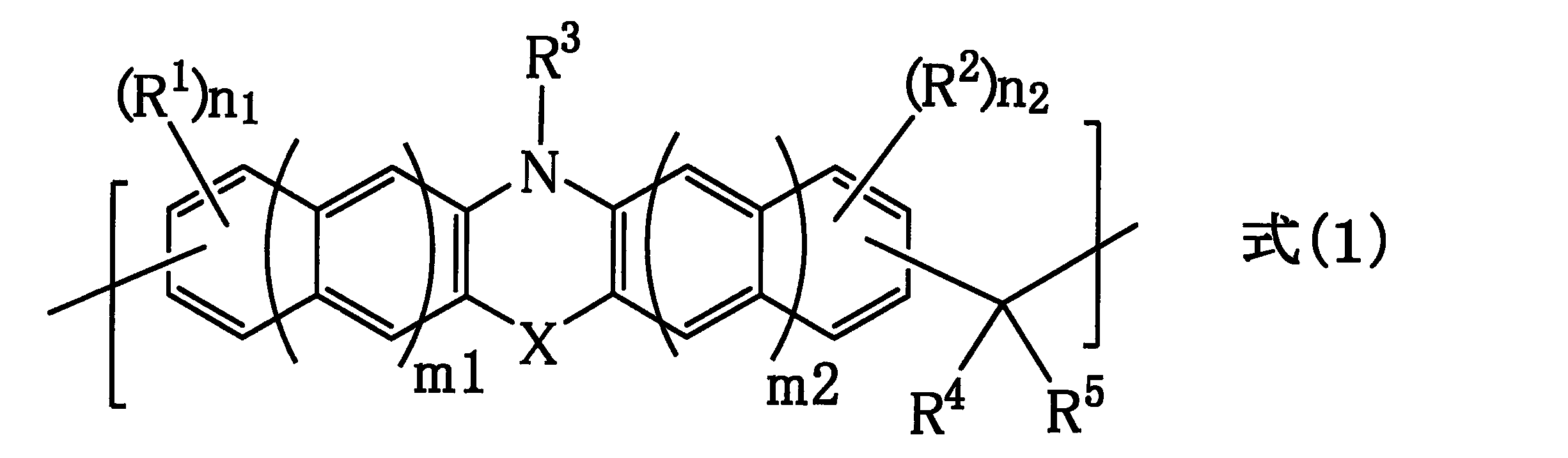
(式(1)中、R1及びR2はそれぞれ芳香環上の水素原子の置換基であって、互いに独立して、ハロゲン基、ニトロ基、アミノ基、カルボン酸基、ヒドロキシ基、炭素数1乃至10のアルキル基、炭素数2乃至10のアルケニル基、炭素数6乃至40のアリール基、エーテル結合を含む有機基、ケトン結合を含む有機基、エステル結合を含む有機基、又はそれらを組み合わせた基であり、
R3は水素原子、又は炭素数1乃至10のアルキル基、炭素数2乃至10のアルケニル基、炭素数6乃至40のアリール基、エーテル結合を含む有機基、ケトン結合を含む有機基、エステル結合を含む有機基、若しくはそれらの組み合わせた基であり、
R4は炭素数6乃至40のアリール基又は複素環基であり、かつ、該アリール基及び該複素環基はそれぞれハロゲン基、ニトロ基、アミノ基、炭素数1乃至10のアルキル基、炭素数1乃至10のアルコキシ基、炭素数6乃至40のアリール基、ホルミル基、カルボキシル基、カルボン酸エステル基、又は水酸基で置換されていても良く、
R5は水素原子、炭素数1乃至10のアルキル基、炭素数6乃至40のアリール基、又は複素環基であり、かつ、該アルキル基、該アリール基、及び該複素環基はそれぞれハロゲン基、ニトロ基、アミノ基、又は水酸基で置換されていても良く、そしてR4とR5はそれらが結合する炭素原子と一緒になって環を形成していても良く、
XはO原子、S原子、CH2基、C=O基、CH=CH基、又はCH2-CH2基であり、n1及びn2はそれぞれ0乃至3の整数であり、m1及びm2はそれぞれ0乃至3の整数を示す。)で表される単位構造を含むポリマーを含むレジスト下層膜形成組成物、
第2観点として、下記式(2):
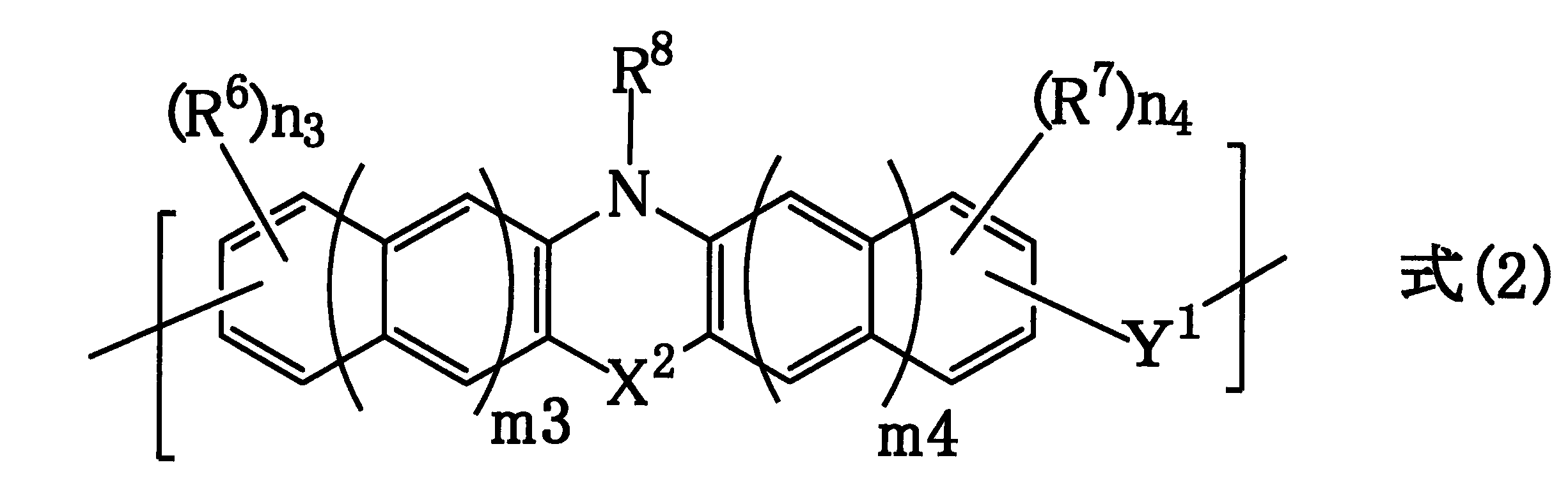
(式(2)中、R6及びR7はそれぞれ芳香環上の水素原子の置換基であって、互いに独立して、ハロゲン基、ニトロ基、アミノ基、カルボン酸基、ヒドロキシ基、炭素数1乃至10のアルキル基、炭素数2乃至10のアルケニル基、炭素数6乃至40のアリール基、エーテル結合を含む有機基、ケトン結合を含む有機基、エステル結合を含む有機基、又はそれらを組み合わせた基であり、
R8は水素原子、又は炭素数1乃至10のアルキル基、炭素数2乃至10のアルケニル基、炭素数6乃至40のアリール基、エーテル結合を含む有機基、ケトン結合を含む有機基、エステル結合を含む有機基、若しくはそれらの組み合わせた基であり、
X2はO原子、S原子、CH2基、C=O基、CH=CH基、又はCH2-CH2基であり、
Y1はシクロオレフィン環化合物由来の2価の基であり、
n3及びn4はそれぞれ0乃至3の整数であり、m3及びm4はそれぞれ0乃至3の整数を示す。)で表される単位構造を含むポリマーを含むレジスト下層膜形成組成物、
第3観点として、式(1)においてR3が水素原子である第1観点に記載のレジスト下層膜形成組成物、
第4観点として、式(2)においてR8が水素原子である第2観点に記載のレジスト下層膜形成組成物、
第5観点として、式(1)においてn1及びn2が共に0である第1観点又は第3観点に記載のレジスト下層膜形成組成物、
第6観点として、式(2)においてn3及びn4が共に0である第2観点又は第4観点に記載のレジスト下層膜形成組成物、
第7観点として、ポリマーが請求項1に記載の式(1)で表される単位構造と下記式(3)で表される単位構造:

(式(3)中、Ar1は炭素数6乃至20の芳香族環基であり、R9およびR10はそれぞれ芳香環上の水素原子の置換基であって、R9は水酸基であり、R10はハロゲン基、ニトロ基、アミノ基、炭素数1乃至10のアルキル基、炭素数2乃至10のアルケニル基、炭素数6乃至40のアリール基、エーテル結合を含む有機基、ケトン結合を含む有機基、エステル結合を含む有機基、又はそれらを組み合わせた有機基である。R11は水素原子、又はハロゲン基、ニトロ基、アミノ基、ホルミル基、カルボキシル基、若しくは水酸基で置換されていても良い炭素数6乃至40のアリール基、又は複素環基であり、R12は水素原子、又はハロゲン基、ニトロ基、アミノ基、ホルミル基、カルボキシル基、若しくは水酸基で置換されていても良い炭素数1乃至10のアルキル基、炭素数6乃至40のアリール基、又は複素環基であり、R11とR12はそれらが結合する炭素原子と一緒になって環を形成していても良い。n5は〔1乃至(Ar1環に置換し得る最大の数)〕の整数であり、n6は〔((Ar1環に置換し得る最大の数)-n5)乃至0〕の整数である。)とを含むポリマーである第1観点、第3観点又は第5観点に記載のレジスト下層膜形成組成物、
第8観点として、ポリマーが第2観点に記載の式(2)で表される単位構造と下記式(4)で表される単位構造:

(式(4)中、Ar2は炭素数6乃至20の芳香族環基であり、R13およびR14はそれぞれ芳香環上の水素原子の置換基であって、R13は水酸基であり、R14はハロゲン基、ニトロ基、アミノ基、炭素数1乃至10のアルキル基、炭素数2乃至10のアルケニル基、炭素数6乃至40のアリール基、エーテル結合を含む有機基、ケトン結合を含む有機基、エステル結合を含む有機基、又はそれらを組み合わせた有機基である。Y2はシクロオレフィン環化合物由来の2価の基である。
n7は〔1乃至(Ar2環に置換し得る最大の数)〕の整数であり、n8は〔((Ar2環に置換し得る最大の数)-n7)乃至0〕の整数である。)とを含むポリマーである第2観点、第4観点又は第6観点に記載のレジスト下層膜形成組成物、
第9観点として、更に架橋剤を含む第1観点乃至第8観点のいずれか一つに記載のレジスト下層膜形成組成物、
第10観点として、更に酸及び/又は酸発生剤を含む第1観点乃至第9観点のいずれか一つに記載のレジスト下層膜形成組成物、
第11観点として、第1観点乃至第10観点のいずれか一つに記載のレジスト下層膜形成組成物を半導体基板上に塗布し焼成することによって得られるレジスト下層膜、
第12観点として、第1観点乃至第10観点のいずれか一つに記載のレジスト下層膜形成組成物を半導体基板上に塗布し焼成して下層膜を形成する工程を含む半導体の製造に用いられるレジストパターンの形成方法、
第13観点として、半導体基板上に第1観点乃至第10観点のいずれか一つに記載のレジスト下層膜形成組成物により下層膜を形成する工程、その上にレジスト膜を形成する工程、光又は電子線の照射と現像によりレジストパターンを形成する工程、該レジストパターンにより該下層膜をエッチングする工程、及びパターン化された下層膜により半導体基板を加工する工程を含む半導体装置の製造方法、
第14観点として、半導体基板に第1観点乃至第10観点のいずれか一つに記載のレジスト下層膜形成組成物により下層膜を形成する工程、その上にハードマスクを形成する工程、更にその上にレジスト膜を形成する工程、光又は電子線の照射と現像によりレジストパターンを形成する工程、該レジストパターンによりハードマスクをエッチングする工程、パターン化されたハードマスクにより該下層膜をエッチングする工程、及びパターン化された下層膜により半導体基板を加工する工程を含む半導体装置の製造方法、及び
第15観点として、ハードマスクが無機物の蒸着によるものである第14観点に記載の製造方法である。
また、本発明は式(2)で表される単位構造を含むポリマーを含むレジスト下層膜形成組成物である。
そして、上記ポリマーが式(1)で表される単位構造と上記式(3)で表される単位構造とを含むことができる。
更に、上記ポリマーが式(2)で表される単位構造と上記式(4)で表される単位構造とを含むことができる。
そして、XはO原子、S原子、CH2基、C=O基、CH=CH基、又はCH2-CH2基であり、n1及びn2はそれぞれ0乃至3の整数であり、m1及びm2はそれぞれ0乃至3、又は0乃至1の整数を示す。
R8は水素原子、又は炭素数1乃至10のアルキル基、炭素数2乃至10のアルケニル基、炭素数6乃至40のアリール基、エーテル結合を含む有機基、ケトン結合を含む有機基、エステル結合を含む有機基、若しくはそれらの組み合わせた基であり、
X2はO原子、S原子、CH2基、C=O基、CH=CH基、又はCH2-CH2基であり、
Y1はシクロオレフィン環化合物由来の2価の基であり、
n3及びn4はそれぞれ0乃至3の整数であり、m3及びm4はそれぞれ0乃至3の整数を示す。
n7は〔1乃至(Ar2環に置換し得る最大の数)〕の整数であり、n8は〔((Ar2環に置換し得る最大の数)-n7)乃至0〕の整数である。
炭素数1乃至10のアルキル基としてはメチル基、エチル基、n-プロピル基、i-プロピル基、シクロプロピル基、n-ブチル基、i-ブチル基、s-ブチル基、t-ブチル基、シクロブチル基、1-メチル-シクロプロピル基、2-メチル-シクロプロピル基、n-ペンチル基、1-メチル-n-ブチル基、2-メチル-n-ブチル基、3-メチル-n-ブチル基、1,1-ジメチル-n-プロピル基、1,2-ジメチル-n-プロピル基、2,2-ジメチル-n-プロピル基、1-エチル-n-プロピル基、シクロペンチル基、1-メチル-シクロブチル基、2-メチル-シクロブチル基、3-メチル-シクロブチル基、1,2-ジメチル-シクロプロピル基、2,3-ジメチル-シクロプロピル基、1-エチル-シクロプロピル基、2-エチル-シクロプロピル基、n-ヘキシル基、1-メチル-n-ペンチル基、2-メチル-n-ペンチル基、3-メチル-n-ペンチル基、4-メチル-n-ペンチル基、1,1-ジメチル-n-ブチル基、1,2-ジメチル-n-ブチル基、1,3-ジメチル-n-ブチル基、2,2-ジメチル-n-ブチル基、2,3-ジメチル-n-ブチル基、3,3-ジメチル-n-ブチル基、1-エチル-n-ブチル基、2-エチル-n-ブチル基、1,1,2-トリメチル-n-プロピル基、1,2,2-トリメチル-n-プロピル基、1-エチル-1-メチル-n-プロピル基、1-エチル-2-メチル-n-プロピル基、シクロヘキシル基、1-メチル-シクロペンチル基、2-メチル-シクロペンチル基、3-メチル-シクロペンチル基、1-エチル-シクロブチル基、2-エチル-シクロブチル基、3-エチル-シクロブチル基、1,2-ジメチル-シクロブチル基、1,3-ジメチル-シクロブチル基、2,2-ジメチル-シクロブチル基、2,3-ジメチル-シクロブチル基、2,4-ジメチル-シクロブチル基、3,3-ジメチル-シクロブチル基、1-n-プロピル-シクロプロピル基、2-n-プロピル-シクロプロピル基、1-i-プロピル-シクロプロピル基、2-i-プロピル-シクロプロピル基、1,2,2-トリメチル-シクロプロピル基、1,2,3-トリメチル-シクロプロピル基、2,2,3-トリメチル-シクロプロピル基、1-エチル-2-メチル-シクロプロピル基、2-エチル-1-メチル-シクロプロピル基、2-エチル-2-メチル-シクロプロピル基及び2-エチル-3-メチル-シクロプロピル基等が挙げられる。
式(1)においてn1及びn2が共に0である場合の繰り返し単位構造を用いることができる。
式(1)のR1、R2、R3、及びR5が水素原子であり、R4がベンゼン環、ナフタレン環、又はピレン環である場合を好ましく用いることができる。また、R5とR4が互いに環を形成しフロオレン構造を形成する場合も好ましい。
式(2)においてn3及びn4が共に0である場合の繰り返し単位構造を用いることができる。
また、本発明のポリマーの製造に用いられるケトン類としてはジアリールケトン類であり、例えばジフェニルケトン、フェニルナフチルケトン、ジナフチルケトン、フェニルトリルケトン、ジトリルケトン、9-フルオレノン等が挙げられる。
縮合時の反応温度は通常40℃乃至200℃である。反応時間は反応温度によって種々選択されるが、通常30分乃至50時間程度である。
以上のようにして得られる重合体の重量平均分子量Mwは、通常500乃至1000000、又は600乃至200000である。
以上のようにして得られる重合体の重量平均分子量Mwは、通常500乃至1000000、又は600乃至200000である。

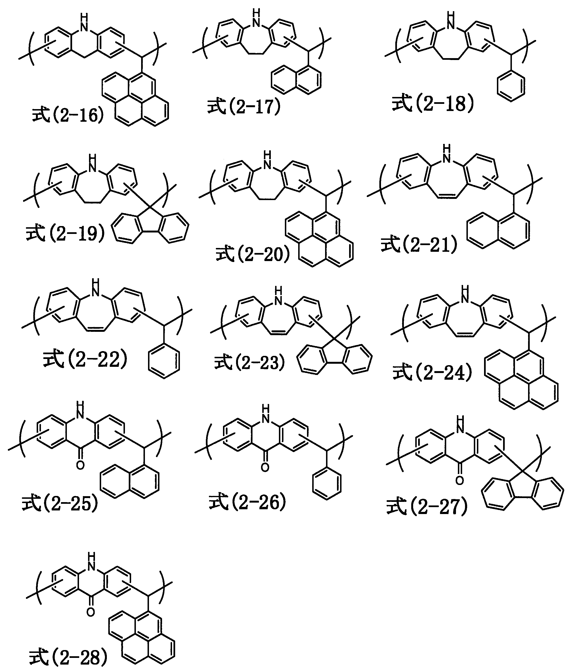

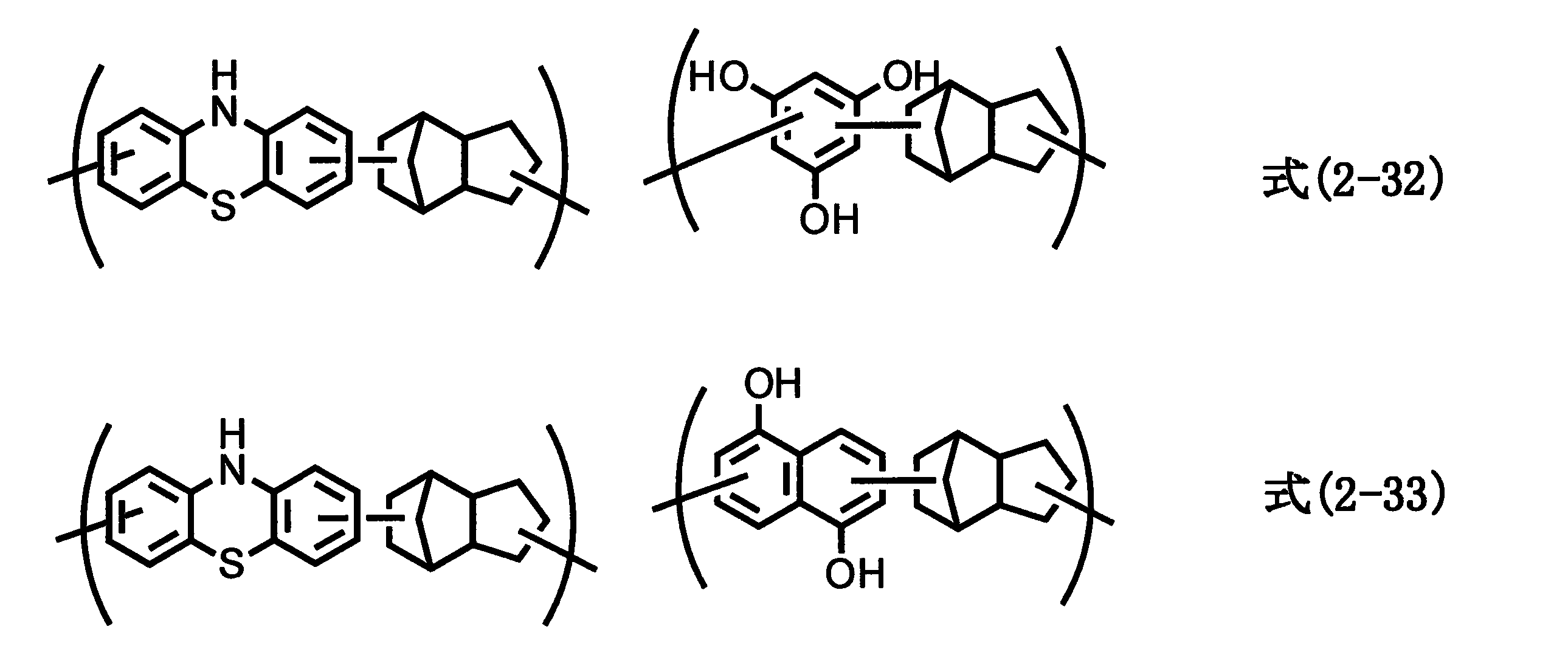
それらポリマーとしてはポリアクリル酸エステル化合物、ポリメタクリル酸エステル化合物、ポリアクリルアミド化合物、ポリメタクリルアミド化合物、ポリビニル化合物、ポリスチレン化合物、ポリマレイミド化合物、ポリマレイン酸無水物、及びポリアクリロニトリル化合物が挙げられる。
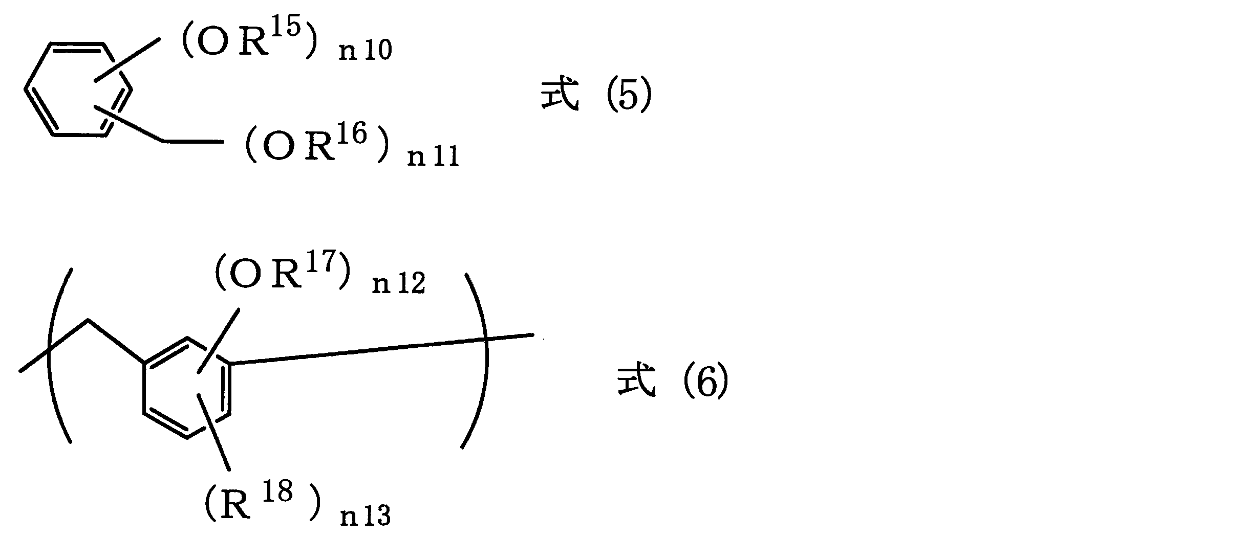
式(6)中、R17は水素原子又は炭素数1乃至10のアルキル基であり、R18は炭素数1乃至10のアルキル基であり、n12は1乃至4の整数であり、n13は0乃至(4-n12)であり、(n12+n13)は1乃至4の整数を示す。オリゴマー及びポリマーは繰り返し単位構造の数が2乃至100、又は2乃至50の範囲で用いることができる。
これらのアルキル基及びアリール基は、上記アルキル基及びアリール基を例示することができる。
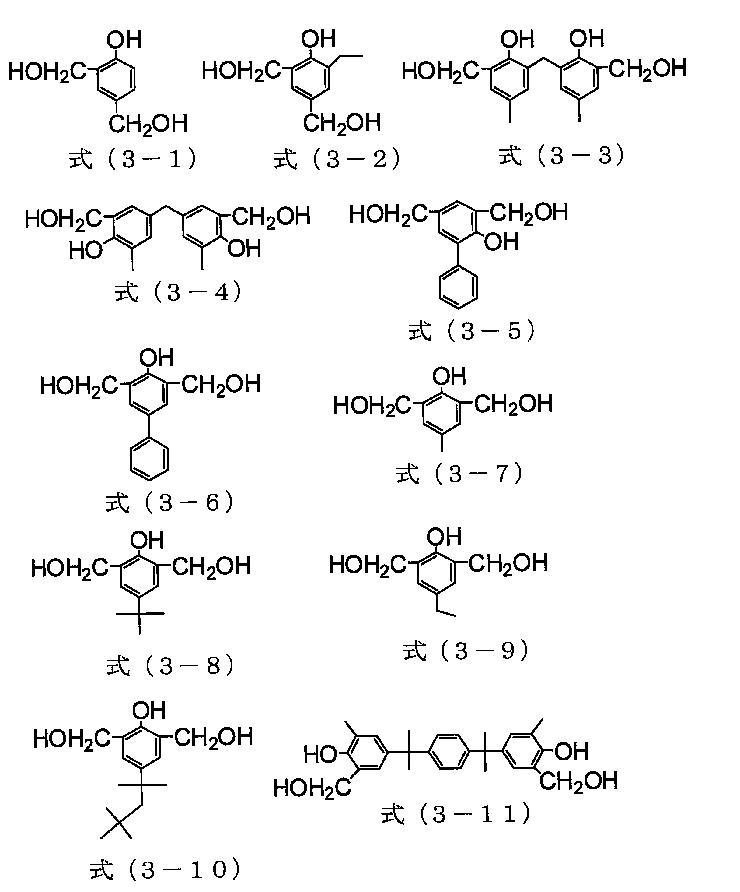

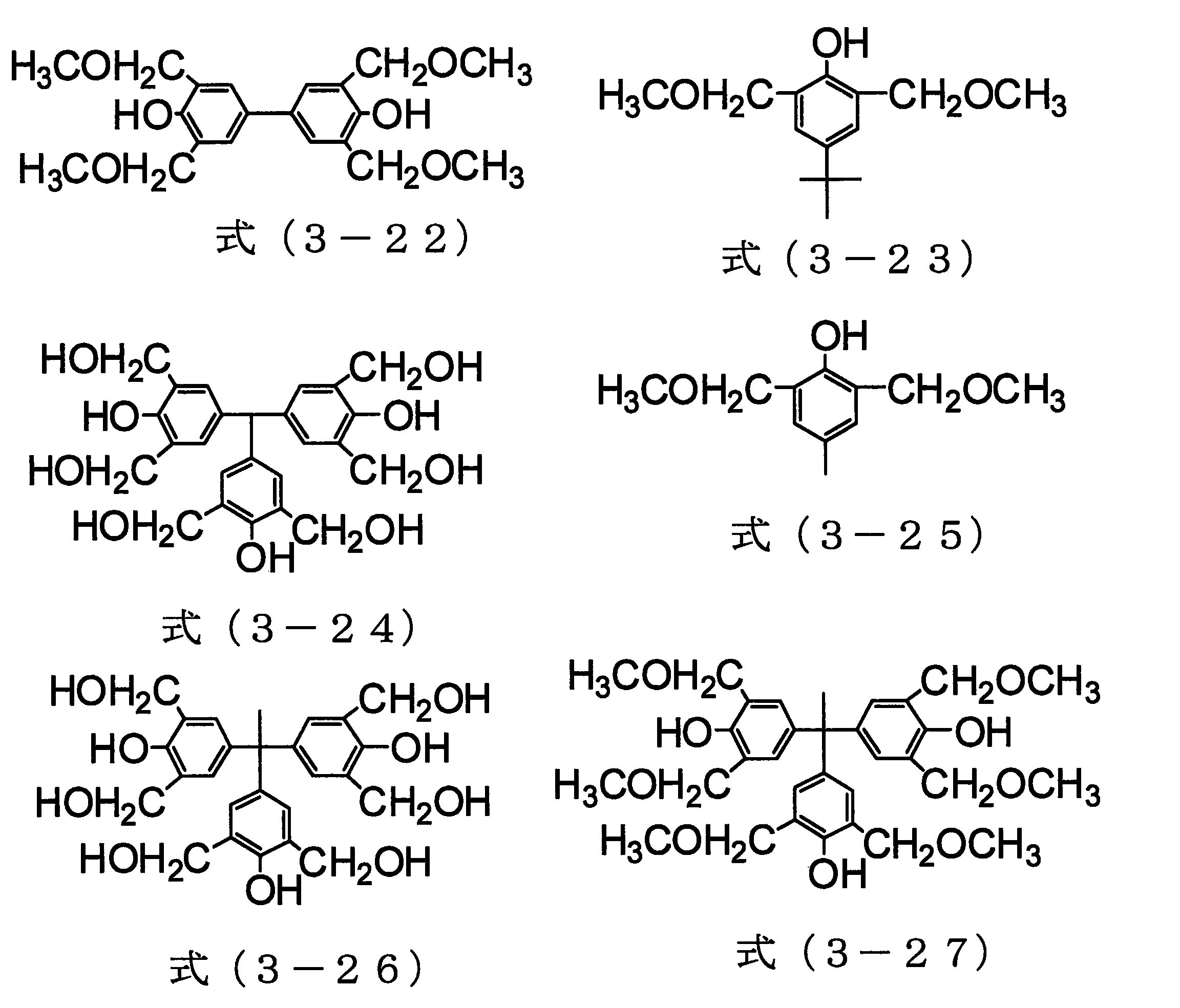
架橋剤の添加量は、使用する塗布溶剤、使用する下地基板、要求される溶液粘度、要求される膜形状などにより変動するが、全固形分に対して0.001乃至80質量%、好ましくは0.01乃至50質量%、さらに好ましくは0.05乃至40質量%である。これら架橋剤は自己縮合による架橋反応を起こすこともあるが、本発明の上記のポリマー中に架橋性置換基が存在する場合は、それらの架橋性置換基と架橋反応を起こすことができる。
更なる吸光剤としては例えば、「工業用色素の技術と市場」(CMC出版)や「染料便覧」(有機合成化学協会編)に記載の市販の吸光剤、例えば、C.I.DisperseYellow1,3,4,5,7,8,13,23,31,49,50,51,54,60,64,66,68,79,82,88,90,93,102,114及び124;C.I.D isperseOrange1,5,13,25,29,30,31,44,57,72及び73;C.I.DisperseRed1,5,7,13,17,19,43,50,54,58,65,72,73,88,117,137,143,199及び210;C.I.DisperseViolet43;C.I.DisperseBlue 96;C.I.Fluorescent Brightening Agent 112,135及び163;C.I.SolventOrange2及び45;C.I.SolventRed1,3,8,23,24,25,27及び49;C.I.Pigment Green 10;C.I.PigmentBrown 2等を好適に用いることができる。上記吸光剤は通常、リソグラフィー用レジスト下層膜材料の全固形分に対して10質量%以下、好ましくは5質量%以下の割合で配合される。
また電子線レジストの電子線照射は、例えば電子線照射装置を用い照射することができる。
100mlナスフラスコにフェノチアジン(東京化成工業株式会社製)8.0g、1-ナフトアルデヒド(東京化成工業株式会社製)6.3g、p-トルエンスルホン酸一水和物(東京化成工業株式会社製)0.81g、1,4-ジオキサン(関東化学製)35.2gを入れた。その後フラスコ内を窒素置換した後加熱し、約28時間還流撹拌した。反応終了後、1,4-ジオキサン(関東化学製)10gで希釈した。希釈液をメタノール/28%アンモニア水(500g/5g)混合溶液中に滴下し、再沈殿させた。得られた沈殿物を吸引ろ過し、ろ物をメタノールで洗浄後、85℃で一晩減圧乾燥しノボラック樹脂を5.8g得た。得られたポリマーは式(2-1)に相当した。GPCによりポリスチレン換算で測定される重量平均分子量Mwは、1,200であった。
100mlナスフラスコにフェノチアジン(東京化成工業株式会社製)12.0g、ベンズアルデヒド(東京化成工業株式会社製)6.4g、p-トルエンスルホン酸一水和物(東京化成工業株式会社製)1.2g、1,4-ジオキサン(関東化学製)112.8gを入れた。その後フラスコ内を窒素置換した後加熱し、約26時間還流撹拌した。反応終了後、テトラヒドロフラン(関東化学製)22gで希釈した。希釈液をメタノール750g中に滴下し、再沈殿させた。得られた沈殿物を吸引ろ過し、ろ物をメタノールで洗浄後、85℃で一晩減圧乾燥しノボラック樹脂を2.2g得た。得られたポリマーは式(2-2)に相当した。GPCによりポリスチレン換算で測定される重量平均分子量Mwは、6,800であった。
100mlナスフラスコにフェノチアジン(東京化成工業株式会社製)10.0g、9-フルオレノン(東京化成工業株式会社製)9.1g、p-トルエンスルホン酸一水和物(東京化成工業株式会社製)1.0g、トルエン(関東化学製)46.8gを入れた。その後フラスコ内を窒素置換した後加熱し、約29時間還流撹拌した。反応終了後、テトラヒドロフラン(関東化学製)10.4gで希釈した。希釈液をメタノール800mlへ滴下し、再沈殿させた。得られた沈殿物を吸引ろ過し、ろ物をメタノールで洗浄後、85℃で一晩減圧乾燥しノボラック樹脂を12.4g得た。得られたポリマーは式(2-3)に相当した。GPCによりポリスチレン換算で測定される重量平均分子量Mwは、800であった。
100mlナスフラスコにフェノキサジン(東京化成工業株式会社製)5.22g、1-ナフトアルデヒド(東京化成工業株式会社製)4.45g、p-トルエンスルホン酸一水和物(東京化成工業株式会社製)0.67g、トルエン(関東化学製)11.93g、1,4-ジオキサン(関東化学製)11.93gを入れた。その後フラスコ内を窒素置換した後加熱し、約30時間還流撹拌した。反応終了後、1,4-ジオキサン(関東化学製)10.0gで希釈した。希釈液をメタノール500mlへ滴下し、再沈殿させた。得られた沈殿物を吸引ろ過し、ろ物をメタノールで洗浄後、85℃で一晩減圧乾燥しノボラック樹脂を4.4g得た。得られたポリマーは式(2-9)に相当した。GPCによりポリスチレン換算で測定される重量平均分子量Mwは、2,500であった。
300mlナスフラスコにフェノチアジン(東京化成工業株式会社製)20.0g、フロログルシノール(東京化成工業株式会社製)12.7g、1-ナフトアルデヒド(東京化成工業株式会社製)33.5g、メタンスルホン酸(東京化成工業株式会社製)2.0g、プロピレングルコールモノメチルエーテル154.1gを入れた。その後約8時間還流撹拌した。反応終了後、反応液をメタノール中に滴下し、再沈殿させた。得られた沈殿物を吸引ろ過し、ろ物をメタノールで洗浄後、85℃で一晩減圧乾燥しノボラック樹脂を28.1g得た。得られたポリマーは式(2-29)に相当した。GPCによりポリスチレン換算で測定される重量平均分子量Mwは、1,100であった。
100mlナスフラスコにフェノチアジン(東京化成工業株式会社製)7.0g、1,5-ジヒドロキシナフタレン(東京化成工業株式会社製)5.6g、1-ナフトアルデヒド(東京化成工業株式会社製)10.2g、メタンスルホン酸(東京化成工業株式会社製)0.67g、プロピレングルコールモノメチルエーテル55.2gを入れた。その後約3時間還流撹拌した。反応終了後、反応液をメタノール中に滴下し、再沈殿させた。得られた沈殿物を吸引ろ過し、ろ物をメタノールで洗浄後、85℃で一晩減圧乾燥しノボラック樹脂を12.2g得た。得られたポリマーは式(2-30)に相当した。GPCによりポリスチレン換算で測定される重量平均分子量Mwは、4,300であった。
100mlナスフラスコにフェノチアジン(東京化成工業株式会社製)15.0g、ジシクロペンタジエン(東京化成工業株式会社製)9.97g、トリフルオロメタンスルホン酸(東京化成工業株式会社製)1.1g、ブチルセロソルブ46.4gを入れた。その後約8時間還流撹拌した。反応終了後、反応液をメタノール中に滴下し、再沈殿させた。得られた沈殿物を吸引ろ過し、ろ物をメタノールで洗浄後、85℃で一晩減圧乾燥し共重合樹脂を12.2g得た。得られたポリマーは式(2-31)に相当した。GPCによりポリスチレン換算で測定される重量平均分子量Mwは、2,500であった。
100mlナスフラスコにフェノチアジン(東京化成工業株式会社製)13.0g、テレフタルアルデヒド酸(東京化成工業株式会社製)9.79g、パラトルエンスルホン酸一水和物(東京化成工業株式会社製)1.31g、ジオキサン56.2gを入れた。その後約8時間還流撹拌した。反応終了後、反応液をメタノール/水(400ml/100ml)の混合液中に滴下し、再沈殿させた。得られた沈殿物を吸引ろ過し、ろ物をメタノールで洗浄後、85℃で一晩減圧乾燥しノボラック樹脂を13.7g得た。得られたポリマーは式(2-7)に相当した。GPCによりポリスチレン換算で測定される重量平均分子量Mwは、2,510であった。
100mlナスフラスコにカルバゾール(東京化成工業株式会社製)8.0g、1-ナフトアルデヒド(東京化成工業株式会社製)28.0g、p-トルエンスルホン酸一水和物(東京化成工業株式会社製)3.6g、トルエン(関東化学製)143.8gを入れた。その後フラスコ内を窒素置換した後加熱し、約27時間還流撹拌した。反応終了後、テトラヒドロフラン(関東化学製)90.5gで希釈した。希釈液をメタノール2000mlへ滴下し、再沈殿させた。得られた沈殿物を吸引ろ過し、ろ物をメタノールで洗浄後、85℃で一晩減圧乾燥しノボラック樹脂を37.9g得た。得られたポリマーは式(7)に相当した。GPCによりポリスチレン換算で測定される重量平均分子量Mwは、3,800であった。

合成例1で得た2gのポリマーに、プロピレングリコールモノメチルエーテルアセテート13.8g、プロピレングリコールモノメチルエーテル4.6g、シクロヘキサノン4.6gに溶解させ、多層膜によるリソグラフィープロセスに用いるレジスト下層膜形成組成物の溶液を調製した。
合成例2で得た2gのポリマーに、プロピレングリコールモノメチルエーテルアセテート13.8g、プロピレングリコールモノメチルエーテル4.6g、シクロヘキサノン4.6gに溶解させ、多層膜によるリソグラフィープロセスに用いるレジスト下層膜形成組成物の溶液を調製した。
合成例3で得た2gのポリマーに、プロピレングリコールモノメチルエーテルアセテート13.8g、プロピレングリコールモノメチルエーテル4.6g、シクロヘキサノン4.6gに溶解させ、多層膜によるリソグラフィープロセスに用いるレジスト下層膜形成組成物の溶液を調製した。
合成例4で得た2gのポリマーに、プロピレングリコールモノメチルエーテルアセテート13.8g、プロピレングリコールモノメチルエーテル4.6g、シクロヘキサノン4.6gに溶解させ、多層膜によるリソグラフィープロセスに用いるレジスト下層膜形成組成物の溶液を調製した。
合成例1で得た2.5gのポリマーに、架橋剤として表されるメチロール化合物(CYTEC製、商品名CYMEL303、下記式(8))0.375g、触媒としてピリジニウムパラトルエンスルホネート0.038g、プロピレングリコールモノメチルエーテルアセテート20.1g、プロピレングリコールモノメチルエーテル6.70g、シクロヘキサノン6.70gに溶解させ、多層膜によるリソグラフィープロセスに用いるレジスト下層膜形成組成物の溶液を調製した。
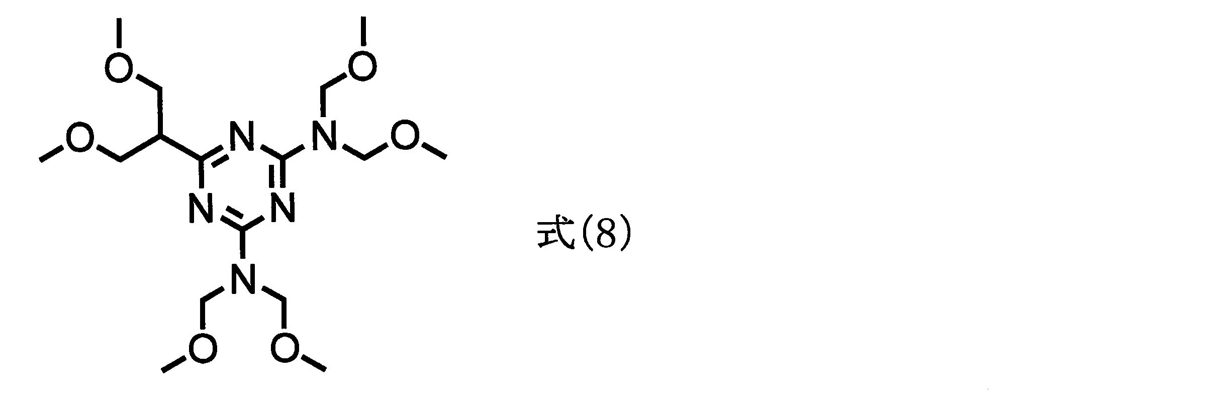
合成例5で得た2gのポリマーに、プロピレングリコールモノメチルエーテルアセテート6.9g、シクロヘキサノン16.1gに溶解させ、多層膜によるリソグラフィープロセスに用いるレジスト下層膜形成組成物の溶液を調製した。
合成例6で得た2gのポリマーに、プロピレングリコールモノメチルエーテルアセテート13.8g、プロピレングリコールモノメチルエーテル9.2gに溶解させ、多層膜によるリソグラフィープロセスに用いるレジスト下層膜形成組成物の溶液を調製した。
合成例7で得た2gのポリマーに、プロピレングリコールモノメチルエーテルアセテート4.6g、シクロヘキサノン18.4gに溶解させ、多層膜によるリソグラフィープロセスに用いるレジスト下層膜形成組成物の溶液を調製した。
合成例8で得た2gのポリマーに、プロピレングリコールモノメチルエーテルアセテート16.1g、プロピレングリコールモノメチルエーテル6.9gに溶解させ、多層膜によるリソグラフィープロセスに用いるレジスト下層膜形成組成物の溶液を調製した。
クレゾールノボラック樹脂(市販品、重量平均分子量は4000)の溶液を使用した。
比較合成例1で得た2gのポリマーに、プロピレングリコールモノメチルエーテルアセテート13.8g、プロピレングリコールモノメチルエーテル4.6g、シクロヘキサノン4.6gに溶解させ、多層膜によるリソグラフィープロセスに用いるレジスト下層膜形成組成物の溶液を調製した。
実施例1乃至9、比較例1乃至2で調製したレジスト下層膜形成組成物の溶液を、スピンコーターを用いてシリコンウェハー上にそれぞれ塗布した。ホットプレート上で240℃1分間もしくは400℃2分間(比較例1は240℃1分間)焼成し、レジスト下層膜(膜厚0.05μm)を形成した。これらのレジスト下層膜を、分光エリプソメーターを用いて波長193nmでの屈折率(n値)及び光学吸光係数(k値、減衰係数とも呼ぶ)を測定した。結果を表1に示した。
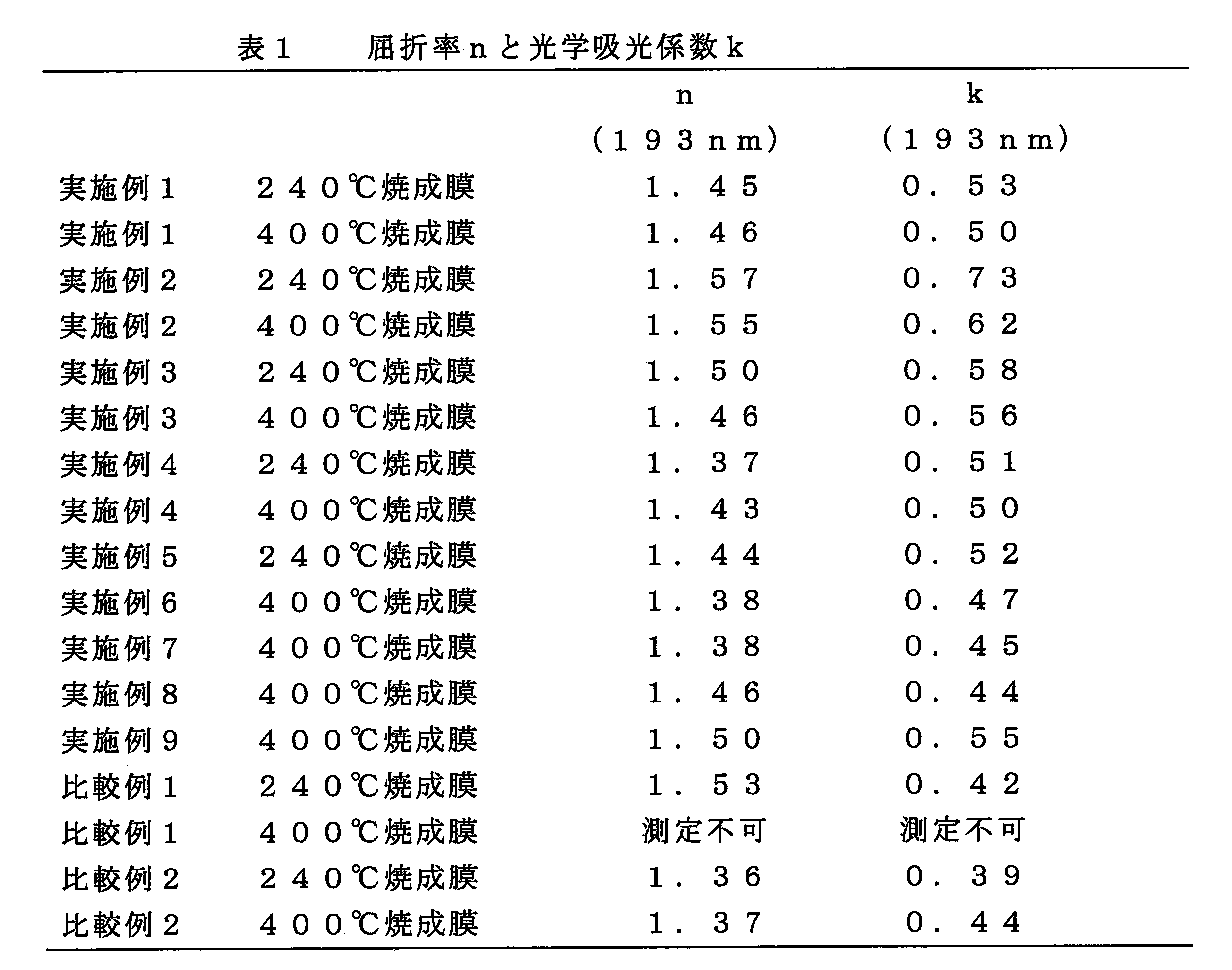
実施例1乃至9、比較例1乃至2で調製したレジスト下層膜形成組成物の溶液を、スピンコーターを用いてシリコンウェハー上にそれぞれ塗布した。ホットプレート上で240℃1分間もしくは400℃2分間焼成し、レジスト下層膜(膜厚0.20μm)を形成した。これらのレジスト下層膜をレジストに使用する溶剤、例えば乳酸エチル、ならびにプロピレングリコールモノメチルエーテル、プロピレングリコールモノメチルエーテルアセテート、シクロヘキサノンに対する浸漬試験を行った。
実施例1乃至実施例4、実施例6乃至実施例9、及び比較例2のレジスト下層膜形成組成物の溶液を240℃1分間焼成した膜は、それらの溶剤に溶解した。また、実施例1乃至実施例9、及び比較例2のレジスト下層膜形成組成物の溶液を400℃2分間焼成した膜は、それらの溶剤に不溶であることを確認した。実施例5、及び比較例1のレジスト下層膜形成組成物の溶液を240℃1分間焼成した膜は、それらの溶剤に不溶であることを確認した。
ドライエッチング速度の測定に用いたエッチャー及びエッチングガスは以下のものを用いた。
RIE-10NR(サムコ製):CF4
実施例1乃至9、及び比較例2で調製したレジスト下層膜形成組成物の溶液を、スピンコーターを用いてシリコンウェハー上に塗布した。ホットプレート上で240℃1分間もしくは400℃2分間焼成し、レジスト下層膜(膜厚0.20μm)を形成した。エッチングガスとしてCF4ガスを使用してドライエッチング速度を測定した。
また、比較例1の溶液を、スピンコーターを用いてシリコンウェハー上に240℃1分間焼成し、レジスト下層膜(膜厚0.20μm)を形成した。エッチングガスとしてCF4ガスを使用してドライエッチング速度を測定し、実施例1乃至9、及び比較例2のレジスト下層膜のドライエッチング速度との比較を行った。結果を表2に示した。速度比は(実施例1乃至9及び比較例2のそれぞれのレジスト下層膜を各温度で焼成した膜のドライエッチング速度)/(比較例1のレジスト下層膜を240℃で焼成した膜のドライエッチング速度)のドライエッチング速度比である。
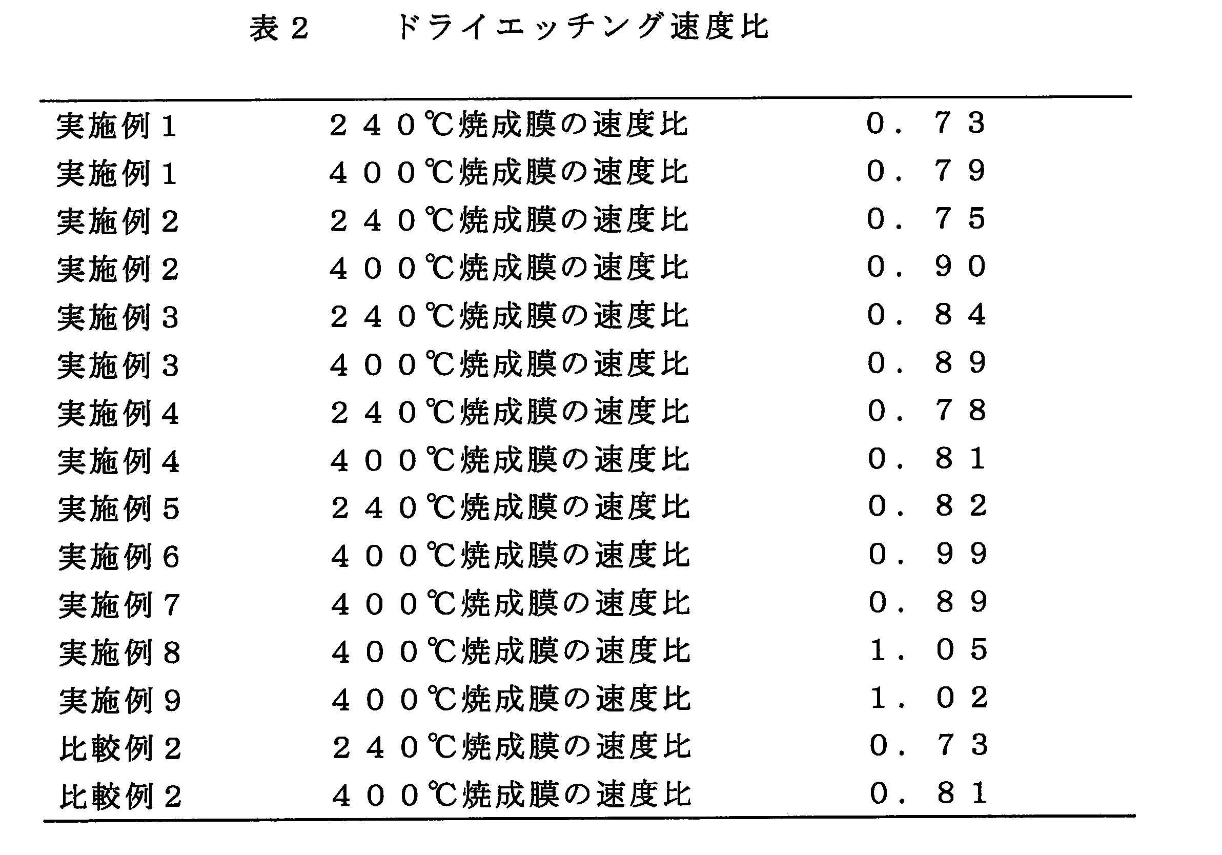
実施例1乃至3、実施例6乃至8、及び比較例2で調整した各レジスト下層膜形成組成物の溶液を、スピンコーターを用いてそれぞれ酸化ケイ素被膜付きシリコンウエハー上に塗布した。ホットプレート上で400℃2分間焼成しレジスト下層膜(膜厚200nm)を形成した。レジスト下層膜上にシリコンハードマスク形成組成物溶液を塗布し、240℃で1分間焼成しシリコンハードマスク層(膜厚45nm)を形成した。その上にレジスト溶液を塗布し、100℃で1分間焼成しレジスト層(膜厚120nm)を形成した。マスクを用いて波長193nmで露光し、露光後加熱PEB(105℃で1分間)を行った後、現像してレジストパターンを得た。その後、フッ素系ガス(成分はCF4)でドライエッチングを行い、レジストパターンをハードマスクに転写した。その後、酸素系ガス(成分はO2/CO2)でドライエッチングを行い、レジストパターンを本件レジスト下層膜に転写した。その後、フッ素系ガス(成分はC4F8/O2/Ar)でドライエッチングを行い、シリコンウエハー上の酸化ケイ素被膜の除去を行った。その時のそれぞれのパターン形状を電子顕微鏡で観察した。
パターンの曲がり(wiggling)が発生することで忠実なパターンに基づく基板加工ができなくなるため、パターンの曲がり(wiggling)が発生する直前のパターン幅(限界パターン幅)により基板加工をする必要がある。
パターンの曲がり(wiggling)が発生し始めるパターン幅は、その値が狭ければ狭いほど微細な基板の加工が可能となる。解像度の測定には測長走査型電子顕微鏡(日立製作所製)を用いた。測定結果を表3に示した。
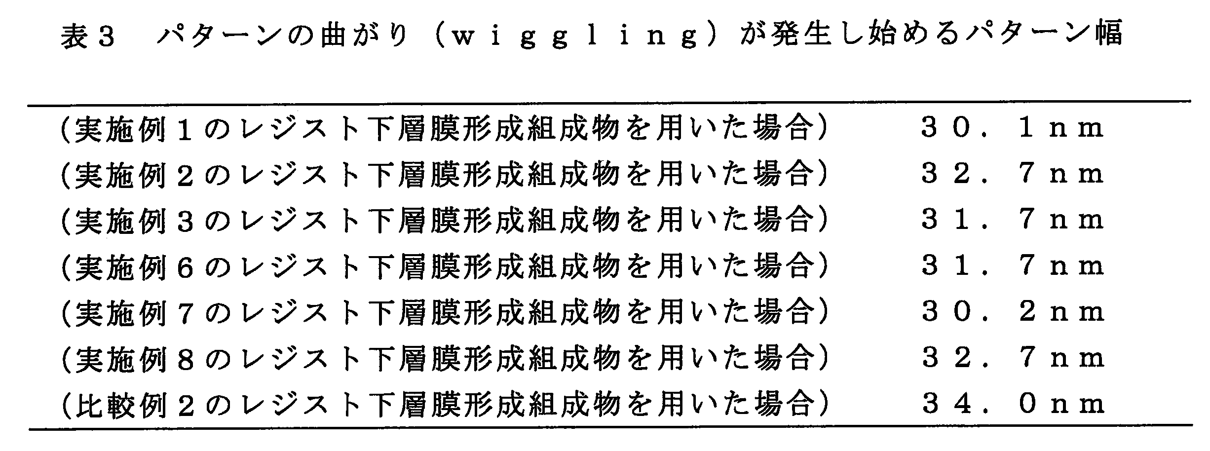
実施例1乃至2、及び比較例2で得た本発明のリソグラフィー用下層膜形成組成物の溶液をスピンコーターにより、ホール(直径0.13μm、深さ0.7μm)を有するSiO2付きウエハー基板上に塗布した。パターンは、ホール中心から隣のホール中心までの間隔が、当該ホールの直径の1倍であるパターンである。

本発明の下層膜材料は上層に蒸着でハードマスクを形成可能な耐熱性を有することが判った。
Claims (15)
- 下記式(1):

(式(1)中、R1及びR2はそれぞれ芳香環上の水素原子の置換基であって、互いに独立して、ハロゲン基、ニトロ基、アミノ基、カルボン酸基、ヒドロキシ基、炭素数1乃至10のアルキル基、炭素数2乃至10のアルケニル基、炭素数6乃至40のアリール基、エーテル結合を含む有機基、ケトン結合を含む有機基、エステル結合を含む有機基、又はそれらを組み合わせた基であり、
R3は水素原子、又は炭素数1乃至10のアルキル基、炭素数2乃至10のアルケニル基、炭素数6乃至40のアリール基、エーテル結合を含む有機基、ケトン結合を含む有機基、エステル結合を含む有機基、若しくはそれらの組み合わせた基であり、
R4は炭素数6乃至40のアリール基又は複素環基であり、かつ、該アリール基及び該複素環基はそれぞれハロゲン基、ニトロ基、アミノ基、炭素数1乃至10のアルキル基、炭素数1乃至10のアルコキシ基、炭素数6乃至40のアリール基、ホルミル基、カルボキシル基、カルボン酸エステル基、又は水酸基で置換されていても良く、
R5は水素原子、炭素数1乃至10のアルキル基、炭素数6乃至40のアリール基、又は複素環基であり、かつ、該アルキル基、該アリール基、及び該複素環基はそれぞれハロゲン基、ニトロ基、アミノ基、又は水酸基で置換されていても良く、そしてR4とR5はそれらが結合する炭素原子と一緒になって環を形成していても良く、
XはO原子、S原子、CH2基、C=O基、CH=CH基、又はCH2-CH2基であり、n1及びn2はそれぞれ0乃至3の整数であり、m1及びm2はそれぞれ0乃至3の整数を示す。)で表される単位構造を含むポリマーを含むレジスト下層膜形成組成物。 - 下記式(2):

(式(2)中、R6及びR7はそれぞれ芳香環上の水素原子の置換基であって、互いに独立して、ハロゲン基、ニトロ基、アミノ基、カルボン酸基、ヒドロキシ基、炭素数1乃至10のアルキル基、炭素数2乃至10のアルケニル基、炭素数6乃至40のアリール基、エーテル結合を含む有機基、ケトン結合を含む有機基、エステル結合を含む有機基、又はそれらを組み合わせた基であり、
R8は水素原子、又は炭素数1乃至10のアルキル基、炭素数2乃至10のアルケニル基、炭素数6乃至40のアリール基、エーテル結合を含む有機基、ケトン結合を含む有機基、エステル結合を含む有機基、若しくはそれらの組み合わせた基であり、
X2はO原子、S原子、CH2基、C=O基、CH=CH基、又はCH2-CH2基であり、
Y1はシクロオレフィン環化合物由来の2価の基であり、
n3及びn4はそれぞれ0乃至3の整数であり、m3及びm4はそれぞれ0乃至3の整数を示す。)で表される単位構造を含むポリマーを含むレジスト下層膜形成組成物。 - 式(1)においてR3が水素原子である請求項1に記載のレジスト下層膜形成組成物。
- 式(2)においてR8が水素原子である請求項2に記載のレジスト下層膜形成組成物。
- 式(1)においてn1及びn2が共に0である請求項1又は請求項3に記載のレジスト下層膜形成組成物。
- 式(2)においてn3及びn4が共に0である請求項2又は請求項4に記載のレジスト下層膜形成組成物。
- ポリマーが請求項1に記載の式(1)で表される単位構造と下記式(3)で表される単位構造:
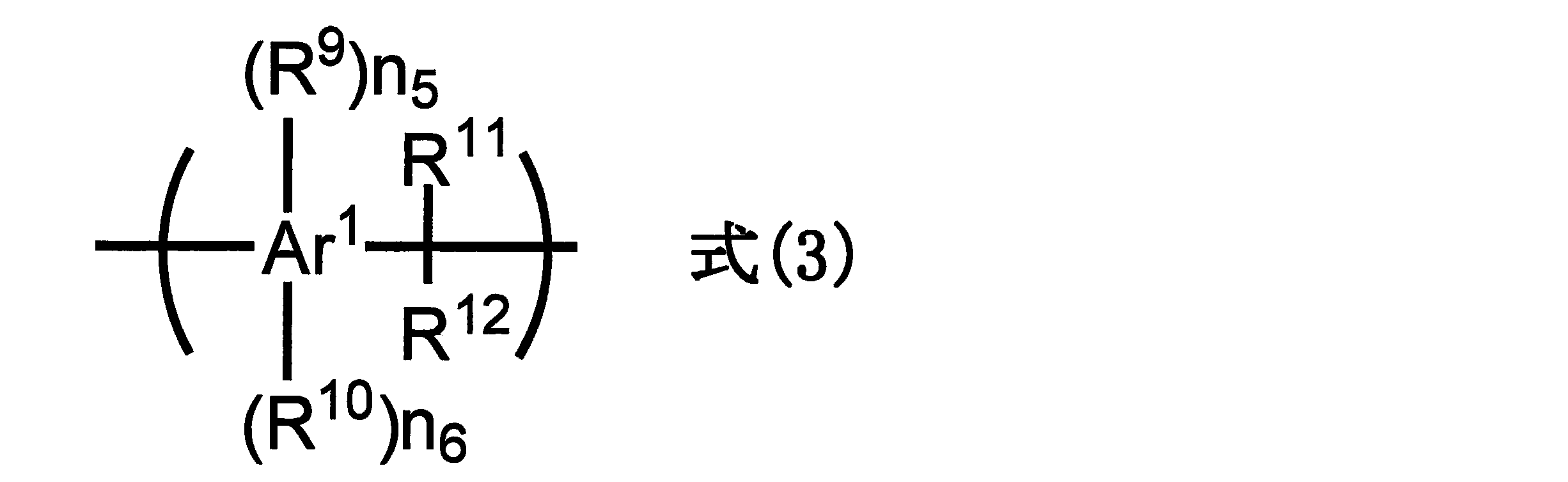
(式(3)中、Ar1は炭素数6乃至20の芳香族環基であり、R9およびR10はそれぞれ芳香環上の水素原子の置換基であって、R9は水酸基であり、R10はハロゲン基、ニトロ基、アミノ基、炭素数1乃至10のアルキル基、炭素数2乃至10のアルケニル基、炭素数6乃至40のアリール基、エーテル結合を含む有機基、ケトン結合を含む有機基、エステル結合を含む有機基、又はそれらを組み合わせた有機基である。R11は水素原子、又はハロゲン基、ニトロ基、アミノ基、ホルミル基、カルボキシル基、若しくは水酸基で置換されていても良い炭素数6乃至40のアリール基、又は複素環基であり、R12は水素原子、又はハロゲン基、ニトロ基、アミノ基、ホルミル基、カルボキシル基、若しくは水酸基で置換されていても良い炭素数1乃至10のアルキル基、炭素数6乃至40のアリール基、又は複素環基であり、R11とR12はそれらが結合する炭素原子と一緒になって環を形成していても良い。n5は〔1乃至(Ar1環に置換し得る最大の数)〕の整数であり、n6は〔((Ar1環に置換し得る最大の数)-n5)乃至0〕の整数である。)とを含むポリマーである請求項1、請求項3又は請求項5に記載のレジスト下層膜形成組成物。 - ポリマーが請求項2に記載の式(2)で表される単位構造と下記式(4)で表される単位構造:
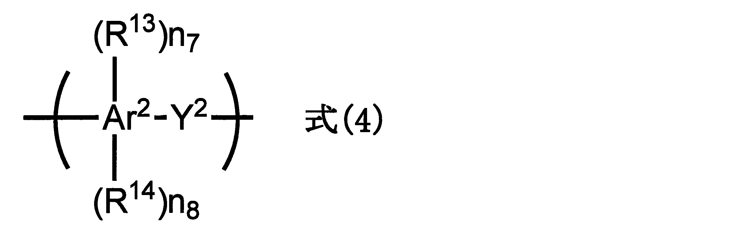
(式(4)中、Ar2は炭素数6乃至20の芳香族環基であり、R13およびR14はそれぞれ芳香環上の水素原子の置換基であって、R13は水酸基であり、R14はハロゲン基、ニトロ基、アミノ基、炭素数1乃至10のアルキル基、炭素数2乃至10のアルケニル基、炭素数6乃至40のアリール基、エーテル結合を含む有機基、ケトン結合を含む有機基、エステル結合を含む有機基、又はそれらを組み合わせた有機基である。Y2はシクロオレフィン環化合物由来の2価の基である。
n7は〔1乃至(Ar2環に置換し得る最大の数)〕の整数であり、n8は〔((Ar2環に置換し得る最大の数)-n7)乃至0〕の整数である。)とを含むポリマーである請求項2、請求項4又は請求項6に記載のレジスト下層膜形成組成物。 - 更に架橋剤を含む請求項1乃至請求項8のいずれか1項に記載のレジスト下層膜形成組成物。
- 更に酸及び/又は酸発生剤を含む請求項1乃至請求項9のいずれか1項に記載のレジスト下層膜形成組成物。
- 請求項1乃至請求項10のいずれか1項に記載のレジスト下層膜形成組成物を半導体基板上に塗布し焼成することによって得られるレジスト下層膜。
- 請求項1乃至請求項10のいずれか1項に記載のレジスト下層膜形成組成物を半導体基板上に塗布し焼成して下層膜を形成する工程を含む半導体の製造に用いられるレジストパターンの形成方法。
- 半導体基板上に請求項1乃至請求項10のいずれか1項に記載のレジスト下層膜形成組成物により下層膜を形成する工程、その上にレジスト膜を形成する工程、光又は電子線の照射と現像によりレジストパターンを形成する工程、該レジストパターンにより該下層膜をエッチングする工程、及びパターン化された下層膜により半導体基板を加工する工程を含む半導体装置の製造方法。
- 半導体基板に請求項1乃至請求項10のいずれか1項に記載のレジスト下層膜形成組成物により下層膜を形成する工程、その上にハードマスクを形成する工程、更にその上にレジスト膜を形成する工程、光又は電子線の照射と現像によりレジストパターンを形成する工程、該レジストパターンによりハードマスクをエッチングする工程、パターン化されたハードマスクにより該下層膜をエッチングする工程、及びパターン化された下層膜により半導体基板を加工する工程を含む半導体装置の製造方法。
- ハードマスクが無機物の蒸着によるものである請求項14に記載の製造方法。
Priority Applications (4)
| Application Number | Priority Date | Filing Date | Title |
|---|---|---|---|
| KR1020147018204A KR102005532B1 (ko) | 2012-02-01 | 2013-01-25 | 복소환을 포함하는 공중합 수지를 포함하는 레지스트 하층막 형성 조성물 |
| CN201380006128.2A CN104067175B (zh) | 2012-02-01 | 2013-01-25 | 含有具有杂环的共聚树脂的抗蚀剂下层膜形成用组合物 |
| US14/370,256 US9261790B2 (en) | 2012-02-01 | 2013-01-25 | Resist underlayer film-forming composition containing copolymer resin having heterocyclic ring |
| JP2013556376A JP6137486B2 (ja) | 2012-02-01 | 2013-01-25 | 複素環を含む共重合樹脂を含むレジスト下層膜形成組成物 |
Applications Claiming Priority (2)
| Application Number | Priority Date | Filing Date | Title |
|---|---|---|---|
| JP2012-020123 | 2012-02-01 | ||
| JP2012020123 | 2012-02-01 |
Publications (1)
| Publication Number | Publication Date |
|---|---|
| WO2013115097A1 true WO2013115097A1 (ja) | 2013-08-08 |
Family
ID=48905137
Family Applications (1)
| Application Number | Title | Priority Date | Filing Date |
|---|---|---|---|
| PCT/JP2013/051598 WO2013115097A1 (ja) | 2012-02-01 | 2013-01-25 | 複素環を含む共重合樹脂を含むレジスト下層膜形成組成物 |
Country Status (6)
| Country | Link |
|---|---|
| US (1) | US9261790B2 (ja) |
| JP (1) | JP6137486B2 (ja) |
| KR (1) | KR102005532B1 (ja) |
| CN (1) | CN104067175B (ja) |
| TW (1) | TWI579647B (ja) |
| WO (1) | WO2013115097A1 (ja) |
Cited By (14)
| Publication number | Priority date | Publication date | Assignee | Title |
|---|---|---|---|---|
| WO2015098594A1 (ja) * | 2013-12-26 | 2015-07-02 | 日産化学工業株式会社 | 第二アミノ基を有するノボラックポリマーを含むレジスト下層膜形成組成物 |
| JP2015124292A (ja) * | 2013-12-26 | 2015-07-06 | 日産化学工業株式会社 | イミノスチルベンポリマー及びそれを含むレジスト下層膜形成組成物 |
| WO2015194273A1 (ja) * | 2014-06-16 | 2015-12-23 | 日産化学工業株式会社 | レジスト下層膜形成組成物 |
| JP2017092457A (ja) * | 2015-10-23 | 2017-05-25 | 三星エスディアイ株式会社Samsung SDI Co., Ltd. | 膜構造物の製造方法およびパターン形成方法 |
| US9758612B2 (en) | 2015-02-17 | 2017-09-12 | Samsung Sdi Co., Ltd. | Polymer, organic layer composition, organic layer, and method of forming patterns |
| WO2018051930A1 (ja) * | 2016-09-16 | 2018-03-22 | Jsr株式会社 | レジスト下層膜形成用組成物、レジスト下層膜及びその形成方法並びにパターニングされた基板の製造方法 |
| KR20190024785A (ko) | 2017-08-28 | 2019-03-08 | 신에쓰 가가꾸 고교 가부시끼가이샤 | 유기막 형성용 조성물, 반도체 장치 제조용 기판, 유기막의 형성 방법, 패턴 형성 방법 및 중합체 |
| KR20190024779A (ko) | 2017-08-30 | 2019-03-08 | 신에쓰 가가꾸 고교 가부시끼가이샤 | 유기막 형성용 조성물, 반도체 장치 제조용 기판, 유기막의 형성 방법, 패턴 형성 방법 및 중합체 |
| US10340148B2 (en) | 2015-10-19 | 2019-07-02 | Samsung Sdi Co., Ltd. | Polymer, organic layer composition, and method of forming patterns |
| JP2019200244A (ja) * | 2018-05-14 | 2019-11-21 | 三菱瓦斯化学株式会社 | リソグラフィー用膜形成材料、リソグラフィー用膜形成用組成物、リソグラフィー用下層膜及びパターン形成方法 |
| WO2019225614A1 (ja) * | 2018-05-25 | 2019-11-28 | 日産化学株式会社 | 環式カルボニル化合物を用いたレジスト下層膜形成組成物 |
| JP2020501336A (ja) * | 2016-10-13 | 2020-01-16 | ヨンチャン ケミカル カンパニー リミテッドYoung Chang Chemical Co.,Ltd | 高耐エッチング性スピンオンカーボンハードマスク組成物及びそれを用いたパターン化方法 |
| EP3623867A1 (en) | 2018-09-13 | 2020-03-18 | Shin-Etsu Chemical Co., Ltd. | Patterning process |
| US11720024B2 (en) | 2015-12-01 | 2023-08-08 | Nissan Chemical Industries, Ltd. | Resist underlayer film-forming composition containing indolocarbazole novolak resin |
Families Citing this family (19)
| Publication number | Priority date | Publication date | Assignee | Title |
|---|---|---|---|---|
| US11592747B2 (en) * | 2012-12-14 | 2023-02-28 | Nissan Chemical Industries, Ltd. | Resist underlayer film-forming composition comprising carbonyl-containing polyhydroxy aromatic ring novolac resin |
| KR102313101B1 (ko) | 2013-12-12 | 2021-10-15 | 롬 앤드 하스 일렉트로닉 머트어리얼즈 엘엘씨 | 하부층용 방향족 수지 |
| KR101798935B1 (ko) * | 2015-04-10 | 2017-11-17 | 삼성에스디아이 주식회사 | 유기막 조성물, 유기막, 및 패턴형성방법 |
| US9908990B2 (en) | 2015-04-17 | 2018-03-06 | Samsung Sdi Co., Ltd. | Organic layer composition, organic layer, and method of forming patterns |
| US9873815B2 (en) * | 2015-04-30 | 2018-01-23 | Samsung Sdi Co., Ltd. | Polymer, organic layer composition, and method of forming patterns |
| US9971243B2 (en) * | 2015-06-10 | 2018-05-15 | Samsung Sdi Co., Ltd. | Polymer, organic layer composition, organic layer, and method of forming patterns |
| KR101895908B1 (ko) * | 2015-06-10 | 2018-10-24 | 삼성에스디아이 주식회사 | 중합체, 유기막 조성물, 및 패턴형성방법 |
| KR101884447B1 (ko) | 2015-07-06 | 2018-08-01 | 삼성에스디아이 주식회사 | 모노머, 유기막 조성물, 유기막, 및 패턴형성방법 |
| KR101848344B1 (ko) | 2015-10-23 | 2018-04-12 | 삼성에스디아이 주식회사 | 중합체, 유기막 조성물, 및 패턴형성방법 |
| KR101976016B1 (ko) * | 2016-08-30 | 2019-05-07 | 삼성에스디아이 주식회사 | 중합체, 유기막 조성물 및 패턴형성방법 |
| KR20180027989A (ko) * | 2016-09-07 | 2018-03-15 | 동우 화인켐 주식회사 | 하드마스크용 조성물 |
| KR102037818B1 (ko) * | 2016-11-10 | 2019-10-29 | 삼성에스디아이 주식회사 | 중합체, 유기막 조성물 및 패턴형성방법 |
| TWI748087B (zh) * | 2017-04-25 | 2021-12-01 | 日商日產化學工業股份有限公司 | 使用茀化合物之阻劑下層膜形成組成物 |
| CN111183395A (zh) * | 2017-10-06 | 2020-05-19 | 三井化学株式会社 | 下层膜形成用树脂材料、抗蚀剂下层膜、抗蚀剂下层膜的制造方法及层叠体 |
| JP7145217B2 (ja) * | 2017-12-20 | 2022-09-30 | メルク パテント ゲゼルシャフト ミット ベシュレンクテル ハフツング | エチニル誘導体コンポジット、それを含んでなる組成物、それによる塗膜の製造方法、およびその塗膜を含んでなる素子の製造方法 |
| CN111492311A (zh) * | 2017-12-22 | 2020-08-04 | 日产化学株式会社 | 具有缩醛结构的保护膜形成用组合物 |
| KR102064590B1 (ko) * | 2018-04-10 | 2020-01-09 | 최상준 | 반사방지용 하드마스크 조성물 |
| TW202040276A (zh) * | 2019-02-07 | 2020-11-01 | 日商三井化學股份有限公司 | 底層膜形成用材料、抗蝕劑底層膜及積層體 |
| CN112194780B (zh) * | 2019-07-08 | 2023-05-05 | 厦门恒坤新材料科技股份有限公司 | 聚合物、硬掩膜组合物及形成图案的方法 |
Citations (6)
| Publication number | Priority date | Publication date | Assignee | Title |
|---|---|---|---|---|
| JPH01304149A (ja) * | 1988-06-02 | 1989-12-07 | Nippon Oil Co Ltd | 高分子組成物 |
| JPH10152636A (ja) * | 1991-05-30 | 1998-06-09 | Ricoh Co Ltd | 磁性インク |
| JP2005128509A (ja) * | 2003-10-03 | 2005-05-19 | Shin Etsu Chem Co Ltd | フォトレジスト下層膜形成材料及びパターン形成方法 |
| JP2007297540A (ja) * | 2006-05-01 | 2007-11-15 | Nippon Steel Chem Co Ltd | カルバゾール骨格含有樹脂、カルバゾール骨格含有エポキシ樹脂、エポキシ樹脂組成物及びその硬化物 |
| WO2010147155A1 (ja) * | 2009-06-19 | 2010-12-23 | 日産化学工業株式会社 | カルバゾールノボラック樹脂 |
| JP2012214720A (ja) * | 2011-03-28 | 2012-11-08 | Shin-Etsu Chemical Co Ltd | ビフェニル誘導体、レジスト下層膜材料、レジスト下層膜形成方法及びパターン形成方法 |
Family Cites Families (13)
| Publication number | Priority date | Publication date | Assignee | Title |
|---|---|---|---|---|
| US5298578A (en) * | 1987-07-30 | 1994-03-29 | Occidental Chemical Corporation | Use of phenothiazine derivatives to inhibit scale build up during polymerization of vinyl chloride |
| JPH01154050A (ja) | 1987-12-10 | 1989-06-16 | Toshiba Corp | パターン形成方法 |
| JP2551632B2 (ja) | 1988-07-11 | 1996-11-06 | 株式会社日立製作所 | パターン形成方法および半導体装置製造方法 |
| EP0496816A4 (en) * | 1989-04-27 | 1992-10-28 | Occidental Chemical Corporation | Polymerization reactor scale prevention |
| JP2793251B2 (ja) | 1989-05-09 | 1998-09-03 | 株式会社東芝 | パターン形成方法 |
| US7303855B2 (en) * | 2003-10-03 | 2007-12-04 | Shin-Etsu Chemical Co., Ltd. | Photoresist undercoat-forming material and patterning process |
| EP1915384B1 (en) * | 2005-08-19 | 2012-01-11 | Dow Corning Toray Co., Ltd. | A method of manufacturing an organic silicon compound that contains a methacryloxy group or an acryloxy group |
| JP5247997B2 (ja) | 2005-08-19 | 2013-07-24 | 東レ・ダウコーニング株式会社 | メタクリロキシ基またはアクリロキシ基含有有機ケイ素化合物の製造方法 |
| KR100665758B1 (ko) | 2005-09-15 | 2007-01-09 | 제일모직주식회사 | 반사방지성을 갖는 하드마스크 조성물 |
| JP4421566B2 (ja) | 2005-12-26 | 2010-02-24 | チェイル インダストリーズ インコーポレイテッド | フォトレジスト下層膜用ハードマスク組成物及びこれを利用した半導体集積回路デバイスの製造方法 |
| JP4659678B2 (ja) | 2005-12-27 | 2011-03-30 | 信越化学工業株式会社 | フォトレジスト下層膜形成材料及びパターン形成方法 |
| US7619055B2 (en) * | 2006-04-06 | 2009-11-17 | Xerox Corporation | Linked arylamine polymers and electronic devices generated therefrom |
| US8168369B2 (en) | 2009-02-13 | 2012-05-01 | Lg Chem, Ltd. | Photoactive compound and photosensitive resin composition containing the same |
-
2013
- 2013-01-25 KR KR1020147018204A patent/KR102005532B1/ko active IP Right Grant
- 2013-01-25 CN CN201380006128.2A patent/CN104067175B/zh active Active
- 2013-01-25 JP JP2013556376A patent/JP6137486B2/ja active Active
- 2013-01-25 WO PCT/JP2013/051598 patent/WO2013115097A1/ja active Application Filing
- 2013-01-25 US US14/370,256 patent/US9261790B2/en active Active
- 2013-02-01 TW TW102103980A patent/TWI579647B/zh active
Patent Citations (6)
| Publication number | Priority date | Publication date | Assignee | Title |
|---|---|---|---|---|
| JPH01304149A (ja) * | 1988-06-02 | 1989-12-07 | Nippon Oil Co Ltd | 高分子組成物 |
| JPH10152636A (ja) * | 1991-05-30 | 1998-06-09 | Ricoh Co Ltd | 磁性インク |
| JP2005128509A (ja) * | 2003-10-03 | 2005-05-19 | Shin Etsu Chem Co Ltd | フォトレジスト下層膜形成材料及びパターン形成方法 |
| JP2007297540A (ja) * | 2006-05-01 | 2007-11-15 | Nippon Steel Chem Co Ltd | カルバゾール骨格含有樹脂、カルバゾール骨格含有エポキシ樹脂、エポキシ樹脂組成物及びその硬化物 |
| WO2010147155A1 (ja) * | 2009-06-19 | 2010-12-23 | 日産化学工業株式会社 | カルバゾールノボラック樹脂 |
| JP2012214720A (ja) * | 2011-03-28 | 2012-11-08 | Shin-Etsu Chemical Co Ltd | ビフェニル誘導体、レジスト下層膜材料、レジスト下層膜形成方法及びパターン形成方法 |
Cited By (24)
| Publication number | Priority date | Publication date | Assignee | Title |
|---|---|---|---|---|
| JP2015124292A (ja) * | 2013-12-26 | 2015-07-06 | 日産化学工業株式会社 | イミノスチルベンポリマー及びそれを含むレジスト下層膜形成組成物 |
| JPWO2015098594A1 (ja) * | 2013-12-26 | 2017-03-23 | 日産化学工業株式会社 | 第二アミノ基を有するノボラックポリマーを含むレジスト下層膜形成組成物 |
| WO2015098594A1 (ja) * | 2013-12-26 | 2015-07-02 | 日産化学工業株式会社 | 第二アミノ基を有するノボラックポリマーを含むレジスト下層膜形成組成物 |
| US11199777B2 (en) | 2013-12-26 | 2021-12-14 | Nissan Chemical Industries, Ltd. | Resist underlayer film-forming composition containing novolac polymer having secondary amino group |
| WO2015194273A1 (ja) * | 2014-06-16 | 2015-12-23 | 日産化学工業株式会社 | レジスト下層膜形成組成物 |
| US10191374B2 (en) | 2014-06-16 | 2019-01-29 | Nissan Chemical Industries, Ltd. | Resist underlayer film-forming composition |
| TWI658089B (zh) * | 2014-06-16 | 2019-05-01 | 日商日產化學工業股份有限公司 | 光阻底層膜形成用組成物 |
| US9758612B2 (en) | 2015-02-17 | 2017-09-12 | Samsung Sdi Co., Ltd. | Polymer, organic layer composition, organic layer, and method of forming patterns |
| US10340148B2 (en) | 2015-10-19 | 2019-07-02 | Samsung Sdi Co., Ltd. | Polymer, organic layer composition, and method of forming patterns |
| JP2017092457A (ja) * | 2015-10-23 | 2017-05-25 | 三星エスディアイ株式会社Samsung SDI Co., Ltd. | 膜構造物の製造方法およびパターン形成方法 |
| US11720024B2 (en) | 2015-12-01 | 2023-08-08 | Nissan Chemical Industries, Ltd. | Resist underlayer film-forming composition containing indolocarbazole novolak resin |
| WO2018051930A1 (ja) * | 2016-09-16 | 2018-03-22 | Jsr株式会社 | レジスト下層膜形成用組成物、レジスト下層膜及びその形成方法並びにパターニングされた基板の製造方法 |
| KR20190051972A (ko) * | 2016-09-16 | 2019-05-15 | 제이에스알 가부시끼가이샤 | 레지스트 하층막 형성용 조성물, 레지스트 하층막 및 그의 형성 방법 그리고 패터닝된 기판의 제조 방법 |
| US11215928B2 (en) | 2016-09-16 | 2022-01-04 | Jsr Corporation | Composition for resist underlayer film formation, resist underlayer film and method for forming the same, and production method of a patterned substrate |
| KR102441862B1 (ko) * | 2016-09-16 | 2022-09-08 | 제이에스알 가부시끼가이샤 | 레지스트 하층막 형성용 조성물, 레지스트 하층막 및 그의 형성 방법 그리고 패터닝된 기판의 제조 방법 |
| JP2020501336A (ja) * | 2016-10-13 | 2020-01-16 | ヨンチャン ケミカル カンパニー リミテッドYoung Chang Chemical Co.,Ltd | 高耐エッチング性スピンオンカーボンハードマスク組成物及びそれを用いたパターン化方法 |
| US10998197B2 (en) | 2017-08-28 | 2021-05-04 | Shin-Etsu Chemical Co., Ltd. | Polymer and composition for forming organic film, substrate for manufacturing semiconductor apparatus, method for forming organic film, and patterning process |
| KR20190024785A (ko) | 2017-08-28 | 2019-03-08 | 신에쓰 가가꾸 고교 가부시끼가이샤 | 유기막 형성용 조성물, 반도체 장치 제조용 기판, 유기막의 형성 방법, 패턴 형성 방법 및 중합체 |
| US11181821B2 (en) | 2017-08-30 | 2021-11-23 | Shin-Etsu Chemical Co., Ltd. | Composition for forming organic film, substrate for manufacturing semiconductor apparatus, method for forming organic film, patterning process, and polymer |
| KR20190024779A (ko) | 2017-08-30 | 2019-03-08 | 신에쓰 가가꾸 고교 가부시끼가이샤 | 유기막 형성용 조성물, 반도체 장치 제조용 기판, 유기막의 형성 방법, 패턴 형성 방법 및 중합체 |
| JP2019200244A (ja) * | 2018-05-14 | 2019-11-21 | 三菱瓦斯化学株式会社 | リソグラフィー用膜形成材料、リソグラフィー用膜形成用組成物、リソグラフィー用下層膜及びパターン形成方法 |
| WO2019225614A1 (ja) * | 2018-05-25 | 2019-11-28 | 日産化学株式会社 | 環式カルボニル化合物を用いたレジスト下層膜形成組成物 |
| JPWO2019225614A1 (ja) * | 2018-05-25 | 2021-07-01 | 日産化学株式会社 | 環式カルボニル化合物を用いたレジスト下層膜形成組成物 |
| EP3623867A1 (en) | 2018-09-13 | 2020-03-18 | Shin-Etsu Chemical Co., Ltd. | Patterning process |
Also Published As
| Publication number | Publication date |
|---|---|
| US9261790B2 (en) | 2016-02-16 |
| CN104067175A (zh) | 2014-09-24 |
| US20150011092A1 (en) | 2015-01-08 |
| CN104067175B (zh) | 2018-01-02 |
| KR20140122225A (ko) | 2014-10-17 |
| TW201348886A (zh) | 2013-12-01 |
| JP6137486B2 (ja) | 2017-05-31 |
| TWI579647B (zh) | 2017-04-21 |
| JPWO2013115097A1 (ja) | 2015-05-11 |
| KR102005532B1 (ko) | 2019-07-30 |
Similar Documents
| Publication | Publication Date | Title |
|---|---|---|
| JP6137486B2 (ja) | 複素環を含む共重合樹脂を含むレジスト下層膜形成組成物 | |
| JP5867732B2 (ja) | 水酸基含有カルバゾールノボラック樹脂を含むレジスト下層膜形成組成物 | |
| JP6734569B2 (ja) | ピノールノボラック樹脂を含むレジスト下層膜形成組成物 | |
| JP6004172B2 (ja) | カルボニル基含有カルバゾールノボラックを含むリソグラフィー用レジスト下層膜形成組成物 | |
| JP6094767B2 (ja) | フェニルインドール含有ノボラック樹脂を含むレジスト下層膜形成組成物 | |
| JP6583630B2 (ja) | 第二アミノ基を有するノボラックポリマーを含むレジスト下層膜形成組成物 | |
| JP6066092B2 (ja) | ジアリールアミンノボラック樹脂 | |
| JP6703308B2 (ja) | 芳香族メチロール化合物が反応したノボラック樹脂を含むレジスト下層膜形成組成物 | |
| WO2010147155A1 (ja) | カルバゾールノボラック樹脂 | |
| JP6206677B2 (ja) | カルボニル基含有ポリヒドロキシ芳香環ノボラック樹脂を含むレジスト下層膜形成組成物 | |
| WO2014030579A1 (ja) | 多核フェノール類を有するノボラック樹脂を含むレジスト下層膜形成組成物 | |
| JP2014157169A (ja) | ポリヒドロキシベンゼンノボラック樹脂を含むレジスト下層膜形成組成物 | |
| JP6338048B2 (ja) | イミノスチルベンポリマー及びそれを含むレジスト下層膜形成組成物 | |
| WO2014203757A1 (ja) | トリヒドロキシナフタレンノボラック樹脂を含むレジスト下層膜形成組成物 | |
| WO2023162653A1 (ja) | レジスト下層膜形成組成物 |
Legal Events
| Date | Code | Title | Description |
|---|---|---|---|
| 121 | Ep: the epo has been informed by wipo that ep was designated in this application |
Ref document number: 13743388 Country of ref document: EP Kind code of ref document: A1 |
|
| ENP | Entry into the national phase |
Ref document number: 2013556376 Country of ref document: JP Kind code of ref document: A |
|
| ENP | Entry into the national phase |
Ref document number: 20147018204 Country of ref document: KR Kind code of ref document: A |
|
| WWE | Wipo information: entry into national phase |
Ref document number: 14370256 Country of ref document: US |
|
| NENP | Non-entry into the national phase |
Ref country code: DE |
|
| 122 | Ep: pct application non-entry in european phase |
Ref document number: 13743388 Country of ref document: EP Kind code of ref document: A1 |